EP2910604A1 - Film à haute constante diélectrique - Google Patents
Film à haute constante diélectrique Download PDFInfo
- Publication number
- EP2910604A1 EP2910604A1 EP13848067.8A EP13848067A EP2910604A1 EP 2910604 A1 EP2910604 A1 EP 2910604A1 EP 13848067 A EP13848067 A EP 13848067A EP 2910604 A1 EP2910604 A1 EP 2910604A1
- Authority
- EP
- European Patent Office
- Prior art keywords
- high dielectric
- film
- dielectric film
- electrode
- group
- Prior art date
- Legal status (The legal status is an assumption and is not a legal conclusion. Google has not performed a legal analysis and makes no representation as to the accuracy of the status listed.)
- Granted
Links
Images


Classifications
-
- C—CHEMISTRY; METALLURGY
- C08—ORGANIC MACROMOLECULAR COMPOUNDS; THEIR PREPARATION OR CHEMICAL WORKING-UP; COMPOSITIONS BASED THEREON
- C08J—WORKING-UP; GENERAL PROCESSES OF COMPOUNDING; AFTER-TREATMENT NOT COVERED BY SUBCLASSES C08B, C08C, C08F, C08G or C08H
- C08J5/00—Manufacture of articles or shaped materials containing macromolecular substances
- C08J5/18—Manufacture of films or sheets
-
- C—CHEMISTRY; METALLURGY
- C08—ORGANIC MACROMOLECULAR COMPOUNDS; THEIR PREPARATION OR CHEMICAL WORKING-UP; COMPOSITIONS BASED THEREON
- C08K—Use of inorganic or non-macromolecular organic substances as compounding ingredients
- C08K3/00—Use of inorganic substances as compounding ingredients
- C08K3/18—Oxygen-containing compounds, e.g. metal carbonyls
- C08K3/20—Oxides; Hydroxides
- C08K3/22—Oxides; Hydroxides of metals
-
- C—CHEMISTRY; METALLURGY
- C08—ORGANIC MACROMOLECULAR COMPOUNDS; THEIR PREPARATION OR CHEMICAL WORKING-UP; COMPOSITIONS BASED THEREON
- C08K—Use of inorganic or non-macromolecular organic substances as compounding ingredients
- C08K3/00—Use of inorganic substances as compounding ingredients
- C08K3/34—Silicon-containing compounds
- C08K3/36—Silica
-
- G—PHYSICS
- G02—OPTICS
- G02B—OPTICAL ELEMENTS, SYSTEMS OR APPARATUS
- G02B26/00—Optical devices or arrangements for the control of light using movable or deformable optical elements
- G02B26/004—Optical devices or arrangements for the control of light using movable or deformable optical elements based on a displacement or a deformation of a fluid
- G02B26/005—Optical devices or arrangements for the control of light using movable or deformable optical elements based on a displacement or a deformation of a fluid based on electrowetting
-
- G—PHYSICS
- G02—OPTICS
- G02B—OPTICAL ELEMENTS, SYSTEMS OR APPARATUS
- G02B26/00—Optical devices or arrangements for the control of light using movable or deformable optical elements
- G02B26/02—Optical devices or arrangements for the control of light using movable or deformable optical elements for controlling the intensity of light
-
- G—PHYSICS
- G02—OPTICS
- G02B—OPTICAL ELEMENTS, SYSTEMS OR APPARATUS
- G02B3/00—Simple or compound lenses
- G02B3/12—Fluid-filled or evacuated lenses
- G02B3/14—Fluid-filled or evacuated lenses of variable focal length
-
- H—ELECTRICITY
- H01—ELECTRIC ELEMENTS
- H01G—CAPACITORS; CAPACITORS, RECTIFIERS, DETECTORS, SWITCHING DEVICES, LIGHT-SENSITIVE OR TEMPERATURE-SENSITIVE DEVICES OF THE ELECTROLYTIC TYPE
- H01G4/00—Fixed capacitors; Processes of their manufacture
- H01G4/002—Details
- H01G4/018—Dielectrics
- H01G4/06—Solid dielectrics
- H01G4/14—Organic dielectrics
- H01G4/18—Organic dielectrics of synthetic material, e.g. derivatives of cellulose
-
- H—ELECTRICITY
- H01—ELECTRIC ELEMENTS
- H01G—CAPACITORS; CAPACITORS, RECTIFIERS, DETECTORS, SWITCHING DEVICES, LIGHT-SENSITIVE OR TEMPERATURE-SENSITIVE DEVICES OF THE ELECTROLYTIC TYPE
- H01G4/00—Fixed capacitors; Processes of their manufacture
- H01G4/002—Details
- H01G4/018—Dielectrics
- H01G4/20—Dielectrics using combinations of dielectrics from more than one of groups H01G4/02 - H01G4/06
- H01G4/206—Dielectrics using combinations of dielectrics from more than one of groups H01G4/02 - H01G4/06 inorganic and synthetic material
-
- C—CHEMISTRY; METALLURGY
- C08—ORGANIC MACROMOLECULAR COMPOUNDS; THEIR PREPARATION OR CHEMICAL WORKING-UP; COMPOSITIONS BASED THEREON
- C08J—WORKING-UP; GENERAL PROCESSES OF COMPOUNDING; AFTER-TREATMENT NOT COVERED BY SUBCLASSES C08B, C08C, C08F, C08G or C08H
- C08J2327/00—Characterised by the use of homopolymers or copolymers of compounds having one or more unsaturated aliphatic radicals, each having only one carbon-to-carbon double bond, and at least one being terminated by a halogen; Derivatives of such polymers
- C08J2327/02—Characterised by the use of homopolymers or copolymers of compounds having one or more unsaturated aliphatic radicals, each having only one carbon-to-carbon double bond, and at least one being terminated by a halogen; Derivatives of such polymers not modified by chemical after-treatment
- C08J2327/12—Characterised by the use of homopolymers or copolymers of compounds having one or more unsaturated aliphatic radicals, each having only one carbon-to-carbon double bond, and at least one being terminated by a halogen; Derivatives of such polymers not modified by chemical after-treatment containing fluorine atoms
- C08J2327/16—Homopolymers or copolymers of vinylidene fluoride
-
- C—CHEMISTRY; METALLURGY
- C08—ORGANIC MACROMOLECULAR COMPOUNDS; THEIR PREPARATION OR CHEMICAL WORKING-UP; COMPOSITIONS BASED THEREON
- C08J—WORKING-UP; GENERAL PROCESSES OF COMPOUNDING; AFTER-TREATMENT NOT COVERED BY SUBCLASSES C08B, C08C, C08F, C08G or C08H
- C08J2327/00—Characterised by the use of homopolymers or copolymers of compounds having one or more unsaturated aliphatic radicals, each having only one carbon-to-carbon double bond, and at least one being terminated by a halogen; Derivatives of such polymers
- C08J2327/02—Characterised by the use of homopolymers or copolymers of compounds having one or more unsaturated aliphatic radicals, each having only one carbon-to-carbon double bond, and at least one being terminated by a halogen; Derivatives of such polymers not modified by chemical after-treatment
- C08J2327/12—Characterised by the use of homopolymers or copolymers of compounds having one or more unsaturated aliphatic radicals, each having only one carbon-to-carbon double bond, and at least one being terminated by a halogen; Derivatives of such polymers not modified by chemical after-treatment containing fluorine atoms
- C08J2327/18—Homopolymers or copolymers of tetrafluoroethylene
-
- C—CHEMISTRY; METALLURGY
- C08—ORGANIC MACROMOLECULAR COMPOUNDS; THEIR PREPARATION OR CHEMICAL WORKING-UP; COMPOSITIONS BASED THEREON
- C08K—Use of inorganic or non-macromolecular organic substances as compounding ingredients
- C08K3/00—Use of inorganic substances as compounding ingredients
- C08K3/18—Oxygen-containing compounds, e.g. metal carbonyls
- C08K3/20—Oxides; Hydroxides
- C08K3/22—Oxides; Hydroxides of metals
- C08K2003/2206—Oxides; Hydroxides of metals of calcium, strontium or barium
-
- C—CHEMISTRY; METALLURGY
- C08—ORGANIC MACROMOLECULAR COMPOUNDS; THEIR PREPARATION OR CHEMICAL WORKING-UP; COMPOSITIONS BASED THEREON
- C08K—Use of inorganic or non-macromolecular organic substances as compounding ingredients
- C08K3/00—Use of inorganic substances as compounding ingredients
- C08K3/18—Oxygen-containing compounds, e.g. metal carbonyls
- C08K3/20—Oxides; Hydroxides
- C08K3/22—Oxides; Hydroxides of metals
- C08K2003/2217—Oxides; Hydroxides of metals of magnesium
- C08K2003/222—Magnesia, i.e. magnesium oxide
-
- C—CHEMISTRY; METALLURGY
- C08—ORGANIC MACROMOLECULAR COMPOUNDS; THEIR PREPARATION OR CHEMICAL WORKING-UP; COMPOSITIONS BASED THEREON
- C08K—Use of inorganic or non-macromolecular organic substances as compounding ingredients
- C08K3/00—Use of inorganic substances as compounding ingredients
- C08K3/18—Oxygen-containing compounds, e.g. metal carbonyls
- C08K3/20—Oxides; Hydroxides
- C08K3/22—Oxides; Hydroxides of metals
- C08K2003/2227—Oxides; Hydroxides of metals of aluminium
-
- C—CHEMISTRY; METALLURGY
- C08—ORGANIC MACROMOLECULAR COMPOUNDS; THEIR PREPARATION OR CHEMICAL WORKING-UP; COMPOSITIONS BASED THEREON
- C08K—Use of inorganic or non-macromolecular organic substances as compounding ingredients
- C08K3/00—Use of inorganic substances as compounding ingredients
- C08K3/18—Oxygen-containing compounds, e.g. metal carbonyls
- C08K3/20—Oxides; Hydroxides
- C08K3/22—Oxides; Hydroxides of metals
- C08K2003/2237—Oxides; Hydroxides of metals of titanium
-
- C—CHEMISTRY; METALLURGY
- C08—ORGANIC MACROMOLECULAR COMPOUNDS; THEIR PREPARATION OR CHEMICAL WORKING-UP; COMPOSITIONS BASED THEREON
- C08K—Use of inorganic or non-macromolecular organic substances as compounding ingredients
- C08K2201/00—Specific properties of additives
- C08K2201/002—Physical properties
- C08K2201/003—Additives being defined by their diameter
-
- C—CHEMISTRY; METALLURGY
- C08—ORGANIC MACROMOLECULAR COMPOUNDS; THEIR PREPARATION OR CHEMICAL WORKING-UP; COMPOSITIONS BASED THEREON
- C08L—COMPOSITIONS OF MACROMOLECULAR COMPOUNDS
- C08L2203/00—Applications
- C08L2203/16—Applications used for films
-
- H—ELECTRICITY
- H01—ELECTRIC ELEMENTS
- H01G—CAPACITORS; CAPACITORS, RECTIFIERS, DETECTORS, SWITCHING DEVICES, LIGHT-SENSITIVE OR TEMPERATURE-SENSITIVE DEVICES OF THE ELECTROLYTIC TYPE
- H01G4/00—Fixed capacitors; Processes of their manufacture
- H01G4/002—Details
- H01G4/018—Dielectrics
- H01G4/06—Solid dielectrics
- H01G4/08—Inorganic dielectrics
- H01G4/12—Ceramic dielectrics
- H01G4/1209—Ceramic dielectrics characterised by the ceramic dielectric material
Definitions
- the present invention relates to a high dielectric film.
- High dielectric films have a high dielectric constant, and thus they are proposed to be used as, for example, films for electrowetting.
- the “electrowetting” is a technology of modifying the wettability of a surface of a hydrophobic dielectric film between the hydrophobic (water-repellent) and hydrophilic states in response to the application of an electric field.
- the electrowetting technology enables driving of a conductive liquid on the surface. This mechanism can drive a conductive liquid without any mechanically movable parts, so that it is advantageous to downsizing and life expansion of devices.
- Such a situation leads to proposals in regard to application of electrowetting devices to, in particular, optical elements in display devices, liquid lenses capable of freely changing their focal lengths, and delivery of low-volume liquid in inspection instruments.
- the wettability of a surface of a hydrophobic dielectric film is represented by a contact angle.
- the contact angle ⁇ V between the conductive liquid and the hydrophobic dielectric film with an applied voltage of V is known to be represented by the following formula.
- cos ⁇ v cos ⁇ 0 + ⁇ 0 ⁇ ⁇ 2 ⁇ l ⁇ ⁇ LG ⁇ V 2
- the conductive liquid is driven in response to a change in the wettability of the hydrophobic dielectric film.
- reduction in the voltage for driving a conductive liquid requires reduction in the thickness of a dielectric film or an increase in the dielectric constant.
- hydrophobic films are formed from a fluorine material, but such hydrophobic films have a low dielectric constant (5 or lower).
- Patent Literature 1 proposes a thin dielectric film formed by anodizing only the surface of metal which is to serve as an electrode. This thin dielectric film can prevent generation of pinholes, making it possible to create thinner films of the dielectric film, resulting in a low driving voltage. Still, a more improved technique is demanded which enables driving of a conductive liquid with a lower voltage.
- Patent Literature 2 discloses a film containing a vinylidene fluoride polymer (A) and inorganic oxide particles (B). This film is a hydrophobic dielectric film for electrowetting which enables driving of a conductive liquid with a low voltage.
- the present invention aims to provide a film having a high dielectric constant and a low dissipation factor.
- the present inventors have performed studies on a film having a high dielectric constant and a low dissipation factor, thereby finding that a film comprising a vinylidene fluoride/tetrafluoroethylene copolymer at a specific ratio and including a ( ⁇ -crystal structure at a specific ratio has a high dielectric constant and a low dissipation factor.
- the inventors have completed the present invention.
- the present invention relates to a high dielectric film comprising a vinylidene fluoride/tetrafluoroethylene copolymer (A) with a mole ratio (vinylidene fluoride) / (tetrafluoroethylene) of 95/5 to 80/20 and including an ⁇ -crystal structure and a ⁇ -crystal structure, with the ratio of the ⁇ -crystal structure being 50% or more.
- A vinylidene fluoride/tetrafluoroethylene copolymer
- A a mole ratio (vinylidene fluoride) / (tetrafluoroethylene) of 95/5 to 80/20 and including an ⁇ -crystal structure and a ⁇ -crystal structure, with the ratio of the ⁇ -crystal structure being 50% or more.
- the high dielectric film of the present invention having the above structure has a high dielectric constant and a low dissipation factor.
- the high dielectric film of the present invention comprises a vinylidene fluoride (VdF)/tetrafluoroethylene (TFE) copolymer (A).
- VdF/TFE copolymer (A) satisfies a mole ratio (VdF/TFE) of 95/5 to 80/20.
- VdF/TFE mole ratio
- the high dielectric film of the present invention with a mole ratio (VdF/TFE) within this range has a high dielectric constant and a low dissipation factor. If the mole ratio of VdF is too low, the film disadvantageously has a low dielectric constant.
- the mole ratio (VdF/TFE) is preferably 94/6 to 90/10.
- composition of the VdF/TFE copolymer (A) can be calculated from the integrated values of the peaks assigned to the respective monomer units measured by F-NMR using a nuclear magnetic resonance device.
- the VdF/TFE copolymer (A) may or may not further comprise a polymer unit derived from a monomer that is copolymerizable with VdF and TFE.
- the amount of the polymer unit derived from a monomer that is copolymerizable with VdF and TFE is preferably 0.1 to 10 mol% in 100 mol% of all the polymer units. This amount is more preferably 1 to 5 mol%.
- Examples of the monomer that is copolymerizable with VdF and TFE include fluoroolefins such as chlorotrifluoroethylene (CTFE), trifluoroethylene (TrFE), monofluoroethylene, hexafluoropropylene (HFP), and perfluoro(alkyl vinyl ether) (PAVE); fluoroacrylates; and function-containing fluoromonomers.
- CTFE chlorotrifluoroethylene
- TrFE trifluoroethylene
- HFP hexafluoropropylene
- PAVE perfluoro(alkyl vinyl ether)
- the high dielectric film of the present invention includes an ⁇ -crystal structure and a ( ⁇ -crystal structure, or includes only a. ⁇ -crystal structure.
- the ⁇ -crystal structure constitutes 50% or more of the VdF/TFE copolymer (A). Even though a VdF-rich VdF/TFE copolymer is likely to be occupied with the ⁇ -crystal structure and the high dielectric film of the present invention comprises a VdF-rich VdF/TFE copolymer (A), the most part of the high dielectric film is occupied with the ⁇ -crystal structure. Therefore, the high dielectric film of the present invention is a novel high dielectric film.
- the film has a high dielectric constant and a low dissipation factor.
- the high dielectric film of the present invention is excellent in insulation properties.
- the dielectric constant thereof does not decrease even after long-time application of a high voltage.
- the ratio of the ⁇ -crystal structure is preferably 70% or more, and more preferably 80% or more.
- the ⁇ -crystal structure may account for 100%.
- the ratio of the ⁇ -crystal structure is a value determined from the ratio between the absorbance at the absorption peak (839 cm -1 ) assigned to the ⁇ -crystal and the absorbance at the absorption peak (763 cm -1 ) assigned to the ⁇ -crystal using a Fourier transform infrared (FT-IR) spectrophotometer.
- FT-IR Fourier transform infrared
- the ratio of the ⁇ -crystal structure can be calculated on the basis of the results of the FT-IR determination and the following formula.
- the VdF/TFE copolymer (A) preferably has a melting point of 130°C to 170°C.
- the melting point is more preferably 135°C to 165°C, and still more preferably 140°C to 160°C.
- the melting point of the VdF/TFE copolymer (A) is determined as a temperature corresponding to the local maximum on the heat-of-fusion curve obtained at a temperature-increasing rate of 10°C/min using a differential scanning calorimetry (DSC) device.
- DSC differential scanning calorimetry
- the dielectric constant (25°C, 1 kHz) of the VdF/TFE copolymer (A) is preferably 7 or higher, more preferably 8 or higher, and still more preferably 9 or higher.
- the upper limit of the dielectric constant is not particularly limited, and it is, for example, 12.
- the high dielectric film of the present invention preferably comprises 80% by mass or more, more preferably 85% by mass or more, and still more preferably 90% by mass or more of the VdF/TFE copolymer (A).
- the upper limit of the amount of the VdF/TFE copolymer (A) is not limited, and may be 100% by mass or 99% by mass, for example.
- the high dielectric film of the present invention preferably further comprises inorganic oxide particles (B).
- the inorganic oxide particles (B) give a high dielectric constant to the high dielectric film of the present invention.
- the particles (B) can greatly improve the volume resistivity while maintaining the high dielectric constant.
- the inorganic oxide particles (B) used in the present invention preferably comprise at least one of the following inorganic oxide particles.
- (B1) Inorganic oxide particles of a metal element selected from group 2, group 3, group 4, group 12, or group 13 of the periodic table, or inorganic oxide composite particles thereof.
- the metal element examples include Be, Mg, Ca, Sr, Ba, Y, Ti, Zr, Zn, and Al.
- an oxide of Al, Mg, Y, or Zn is preferred because it can be used for many purposes and is inexpensive, and has a high volume resistivity.
- particles of at least one selected from the group consisting of Al 2 O 3 , MgO, ZrO 2 , Y 2 O 3 , BeO, and MgO ⁇ Al 2 O 3 are preferred because these particles have a high volume resistivity.
- Al 2 O 3 whose crystal structure is the ⁇ type is preferred because it has a large specific surface area and is well dispersible in the VdF/TFE copolymer (A).
- M 1 and M 2 may each include multiple metal elements.
- Preferable examples of the metal element in group 4 include Ti and Zr, and preferable examples of the metal element in group 2 include Mg, Ca, Sr, and Ba.
- particles of at least one selected from the group consisting of BaTiO 3 , SrTiO 3 , CaTiO 3 , MgTiO 3 , BaZrO 3 , SrZrO 3 , CaZrO 3 , and MgZrO 3 are preferred because these particles have a high volume resistivity.
- (B3) Inorganic oxide composite particles of silicon oxide and an oxide of a metal element in group 2, group 3, group 4, group 12, or group 13 of the periodic table.
- Such particles are composite particles of the inorganic oxide particles (B1) and silicon oxide. Specific examples thereof include particles of at least one selected from the group consisting of 3A1 2 O 3 ⁇ 2SiO 2 , 2MgO ⁇ SiO 2 , ZrO 2 ⁇ SiO 2 , and MgO ⁇ SiO 2 .
- the inorganic oxide particles (B) do not necessarily have a high dielectricity, and they may appropriately be selected in accordance with the purpose of the resulting high dielectric film.
- oxide particles (B1) of one inexpensive metal which can be used in many uses, in particular Al 2 O 3 or MgO, can improve the volume resistivity.
- the dielectric constant (1 kHz, 25°C) of the oxide particles (B1) of one metal is typically lower than 100, and preferably 10 or lower.
- the inorganic oxide particles (B) may be metal oxide particles (e.g., one species of the particles (B2) and (B3)) having ferroelectricity (having a dielectric constant (1 kHz, 25°C) of 100 or higher).
- Examples of the inorganic material constituting the ferroelectric metal oxide particles (B2) and (B3) include, but are not limited to, composite metal oxides, and complexes, solid solutions, and sol-gel materials thereof.
- the high dielectric film of the present invention preferably contains 0.01 to 300 parts by mass of the inorganic oxide particles (B) for 100 parts by mass of the copolymer (A).
- the amount of the particles (B) is more preferably 0.1 to 100 parts by mass.
- Too much inorganic oxide particles (B) may be difficult to disperse in the copolymer (A) uniformly, and may deteriorate the electric insulation properties (voltage resistance).
- a high dielectric film in which the amount of the inorganic oxide particles (B) is not smaller than 0.01 parts by mass but smaller than 300 parts by mass for 100 parts by mass of the copolymer (A) is one preferable embodiment of the present invention.
- a film containing 300 parts by mass or more of the particles (B) may be fragile and have a low tensile strength.
- the upper limit of the amount of the particles (B) is more preferably 200 parts by mass, and still more preferably 150 parts by mass. Too less inorganic oxide particles (B) are less likely to improve the electric insulation properties.
- the lower limit of the amount of the particles (B) is more preferably 0.1 parts by mass, still more preferably 0.5 parts by mass, and particularly preferably 1 part by mass.
- the inorganic oxide particles (B) preferably have as small an average primary particle size as possible, and are particularly preferably what is called nanoparticles having an average particle size of 1 ⁇ m or smaller. Even a small amount of such inorganic oxide nanoparticles dispersed uniformly can greatly improve the electric insulation properties of the film.
- the average primary particle size is more preferably 800 nm or smaller, still more preferably 500 nm or smaller, and particularly preferably 300 nm or smaller.
- the average particle size may have any lower limit.
- the average primary particle size is preferably 10 nm or greater, more preferably 20 nm or greater, and still more preferably 50 nm or greater.
- the average primary particle size of the inorganic oxide particles (B) was determined using a laser diffraction scattering particle size distribution analyzer (trade name: LA-920, HORIBA, Ltd.).
- the inorganic oxide particles (B) preferably have a dielectric constant (25°C, 1 kHz) of 10 or higher.
- the dielectric constant of the particles (B) is more preferably 100 or higher, and still more preferably 300 or higher.
- the upper limit is not particularly limited, and is typically about 3000.
- the high dielectric film of the present invention may contain other components such as an affinity improver, if desired.
- An affinity improver can improve the affinity between the inorganic oxide particles (B) and the copolymer (A), allow the inorganic oxide particles (B) to disperse uniformly in the copolymer (A), bond the inorganic oxide particles (B) and the copolymer (A) firmly in the film, suppress generation of voids, and increase the dielectric constant.
- the affinity improver may advantageously be a coupling agent, a surfactant, or an epoxy-containing compound.
- Examples of the "coupling agent" as an affinity improver include organotitanium compounds, organosilane compounds, organozirconium compounds, organoaluminum compounds, and organophosphorus compounds.
- organotitanium compounds include coupling agents such as titanium alkoxylates, titanium chelates, and titanium acylates. Preferable examples among these include titanium alkoxylates and titanium chelates because they have good affinity with the inorganic oxide particles (B).
- tetraisopropyl titanate titanium isopropoxy octylene glycolate, diisopropoxy ⁇ bis(acetylacetonato)titanium, diisopropoxy titanium diisostearate, tetraisopropyl bis(dioctylphosphite)titanate, isopropyl tri(n-aminoethyl-aminoethyl)titanate, and tetra(2,2-diallyloxymethyl-1-butyl)bis(di-tridecyl)phosphite titanate.
- the organosilane compound may be of a high molecular weight type or a low molecular weight type.
- alkoxysilanes such as monoalkoxysilanes, dialkoxysilanes, trialkoxysilanes, and tetraalkoxysilanes.
- vinylsilane, epoxysilane, aminosilane, methacryloxysilane, mercaptosilane, and the like may suitably be used.
- An alkoxysilane can be hydrolyzed to much more improve the volume resistivity (improve the electric insulation properties), which is one effect of surface treatment.
- organozirconium compounds examples include alkoxy zirconium compounds and zirconium chelates.
- organoaluminum compounds examples include alkoxy aluminum compounds and aluminum chelates.
- organophosphorus compounds examples include phosphorous acid esters, phosphoric acid esters, and phosphoric acid chelates.
- the "surfactant" as an affinity improver may be of a high molecular weight type or a low molecular weight type. Examples thereof include nonionic surfactants, anionic surfactants, and cationic surfactants. Preferred are high molecular weight surfactants because they have good heat stability.
- nonionic surfactants examples include polyether derivatives, polyvinylpyrrolidone derivatives, and alcohol derivatives. Preferred among these are polyether derivatives because they have good affinity with the inorganic oxide particles (B).
- anionic surfactants include sulfonic acid and carboxylic acid, and polymers containing a salt of such an acid.
- Preferable examples thereof include acrylic acid derivative-based polymers and methacrylic acid derivative-based polymers because they have good affinity with the copolymer (A).
- cationic surfactant examples include amine-based compounds and nitrogen-containing heterocyclic compounds such as imidazoline, and halogenated salts thereof.
- the "epoxy-containing compound" as an affinity improver may be a low molecular weight compound or a high molecular weight compound. Examples thereof include epoxy compounds and glycidyl compounds. Preferred are low molecular weight compounds having one epoxy group because they have good affinity with the copolymer (A).
- the epoxy-containing compounds include a compound represented by the formula: wherein R represents a hydrogen atom, a methyl group, a C2-C10 hydrocarbon group which may optionally include an oxygen atom or a nitrogen atom, or an optionally substituted aromatic ring; 1 is 0 or 1; m is 0 or 1; and n is an integer of 0 to 10. This is because such a compound is particularly excellent in affinity with the copolymer (A).
- the affinity improver can be used in an amount which does not deteriorate the effects of the present invention.
- the amount of the affinity improver is preferably 0.01 to 30 parts by mass, more preferably 0.1 to 25 parts by mass, and still more preferably 1 to 20 parts by mass for 100 parts by mass of the inorganic oxide particles (B).
- the high dielectric film of the present invention may further contain other additives in amounts which do not deteriorate the effects of the present invention.
- the thickness of the high dielectric film of the present invention depends on the use of the film and, for example, it is preferably 0.01 to 50 ⁇ m, and more preferably 0.1 to 30 ⁇ m.
- the thickness is preferably 15 ⁇ m or smaller, more preferably 10 ⁇ m or smaller, still more preferably 5 ⁇ m or smaller, and particularly preferably 2 ⁇ m or smaller so as to lower a voltage required for driving a conductive liquid.
- the high dielectric film of the present invention is preferably thin. Still, in order to maintain the mechanical strength, the lower limit of the thickness is typically about 10 nm.
- the dielectric constant (measurement conditions: 30°C, 1 kHz or 10 kHz) of the high dielectric film of the present invention is preferably 10 or higher, more preferably 11 or higher, and still more preferably 12 or higher.
- the dielectric constant measured at 90°C also preferably satisfies the above range.
- the high dielectric film of the present invention may be a self-supporting film or may be a coated film.
- the ratio of VdF is low and the ratio of TFE is high, so that the resulting film naturally has a ⁇ -crystal structure.
- the ratio of VdF increases, the film is more likely to have an ⁇ -crystal structure.
- the present inventors have found that a high dielectric film produced by a casting technique in very restricted conditions can have a ⁇ -crystal structure at a high ratio even when a VdF/TFE copolymer with a high VdF ratio is used as a material.
- the high dielectric film of the present invention can be produced by the following novel casting technique.
- the high dielectric film of the present invention can be produced by a method including:
- a drying temperature higher than the melting point of the copolymer (A) in the above production method utilizing a casting technique a high dielectric film including 50% or more of the ⁇ -crystal structure can be produced even from a copolymer containing much VdF and less TFE as a material.
- the drying temperature is more preferably 10°C or more higher than the melting point of the copolymer (A).
- the drying temperature is preferably 160°C or higher, more preferably 170°C or higher, and particularly preferably 175°C or higher, for example.
- the upper limit of the drying temperature preferably falls within a range that causes no creases due to melting or heat shrinkage of a film, and may be 200°C, for example.
- the drying time in the casting production method is preferably 0.75 to 4/3 minutes, and more preferably 1 to 4/3 minutes.
- the drying can be achieved by passing the film through a drying furnace.
- a drying furnace whose total length is 10 m (e.g., 2 m ⁇ 5 pieces), for example, the drying can be achieved by passing the film through the drying furnace at a rate of 7.5 to 10 m/min.
- the casting production method is preferably performed in a cleanroom, and more preferably in a class 1000 or better (e.g. class 500, class 100, class 10, or class 1) cleanroom in conformity with FED-STD-209D (Federal Specifications and Standards).
- a class 1000 or better e.g. class 500, class 100, class 10, or class 1
- the solvent may be any one which allows the copolymer (A) to be uniformly dissolved or dispersed therein.
- a polar organic solvent is preferred.
- the polar organic solvent include ketone solvents, ester solvents, carbonate solvents, cyclic ether solvents, and amide solvents.
- methyl ethyl ketone methyl isobutyl ketone (MIBK), acetone, diethyl ketone, dipropyl ketone, ethyl acetate, methyl acetate, propyl acetate, butyl acetate, ethyl lactate, dimethyl carbonate, diethyl carbonate, dipropyl carbonate, methyl ethyl carbonate, tetrahydrofuran, methyl tetrahydrofuran, dioxane, dimethyl formamide (DMF), and dimethyl acetamide.
- MIBK methyl isobutyl ketone
- acetone diethyl ketone
- dipropyl ketone ethyl acetate
- methyl acetate propyl acetate
- butyl acetate ethyl lactate
- dimethyl carbonate diethyl carbonate
- dipropyl carbonate methyl ethyl carbonate
- Examples of a method of applying a liquid composition to a substrate include knife coating, cast coating, roll coating, gravure coating, blade coating, rod coating, air doctor coating, and slot die coating.
- a method of applying a liquid composition to a substrate include knife coating, cast coating, roll coating, gravure coating, blade coating, rod coating, air doctor coating, and slot die coating.
- Such coating techniques can provide a very thin high dielectric film.
- the high dielectric film of the present invention has a high dielectric constant and a low dissipation factor.
- the film thus enables driving of a conductive liquid at a low voltage, so that it can suitably be used for electrowetting devices in optical elements, display devices, varifocal lenses, optical modulators, optical pickups, optical recording and regenerating devices, developing devices, drop operating devices, and analytical equipment (e.g., chemical, biochemical, or biological analytical equipment which requires removal of a minute conductive liquid for analysis of a sample). Since the high dielectric film of the present invention is flexible, it can suitably be used for the aforementioned various applications.
- the high dielectric film of the present invention has a high dielectric constant and a low dissipation factor, it can suitably be used as a film for film capacitors.
- the high dielectric film since its high dielectricity, which is a characteristic of a vinylidene fluoride-based resin, does not deteriorate even after long term application of a voltage, the high dielectric film is advantageous as a film for film capacitors.
- the high dielectric film of the present invention When the high dielectric film of the present invention is used as a hydrophobic dielectric film in an electrowetting device, an electric charge applied to the surface of the film changes the wettability of the surface, driving the conductive liquid in contact with the surface.
- an electric charge is applied to the surface of the high dielectric film of the present invention, the electric charge is stored on the surface. The Coulomb force of this electric charge then drives the liquid in a short distance.
- the conductive liquid examples include, but are not limited to, water and aqueous solutions containing an electrolyte (e.g. potassium chloride, sodium chloride).
- a conductive liquid is typically a polar liquid.
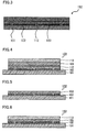
- a laminate may be prepared which comprises a substrate, an electrode disposed on at least part of the substrate, a high dielectric inorganic layer disposed on the substrate such that it covers the electrode, and the high dielectric film of the present invention disposed on the high dielectric inorganic layer (for example, see Fig. 3 ).
- the laminate may further comprise a water-repellent layer on the high dielectric film of the present invention (for example, see Fig. 4 ).
- the water-repellent layer can improve the water repellency of the laminate surface, enabling effective driving of the conductive liquid.
- this electrode is disposed between the substrate and the high dielectric inorganic layer.
- the laminate may comprise no high dielectric inorganic layer.
- a laminate may comprise a substrate, an electrode disposed on at least part of the substrate, and the high dielectric film of the present invention disposed on the substrate such that it covers the electrode (for example, see Fig. 5 ).
- This laminate may further comprise a water-repellent layer on the high dielectric film of the present invention (for example, see Fig. 6 ).
- the laminate may comprise high dielectric film of the present invention and one or more water-repellent layers.
- a laminate may comprise
- the layered structure may further comprise one or more high dielectric inorganic layers.
- the substrate may comprise an optically transparent insulating material such as glass or transparent resin. Still, the material may be any one capable of carrying an electrode thereon.
- the transparent resin include polyethylene terephthalate (PET) resin, polycarbonate (PC) resin, polyimide (PI) resin, poly(methyl methacrylate) (PMMA), and polystyrene resin.
- the substrate may have any thickness, and the thickness may be, for example, 1 ⁇ m to 100 mm.
- the electrode may comprise a transparent conductive material such as indium oxide (In 2 O 3 ), tin dioxide (SnO 2 ), or indium tin oxide (ITO), which is a mixture of In 2 O 3 and SnO 2 .
- the electrode may be an In 2 O 3 film, a SnO 2 film, or an ITO film doped with tin (Sn), antimony (Sb), or fluorine (F).
- the electrode may also comprise magnesium oxide (MgO) or zinc oxide (ZnO), for example.
- the electrode may also be an AZO film (an aluminum-doped (Al-doped) ZnO film), a GZO film (a gallium-doped (Ga-doped) ZnO film), or an indium-doped ZnO film.
- the electrode may also comprise any transparent organic conductive material selected from conductive polymers such as thiophene conductive polymers, polyaniline, and polypyrrole; or any metal material such as aluminum, copper, chromium, nickel, zinc, stainless steel, gold, silver, platinum, tantalum, titanium, niobium, and molybdenum.
- conductive polymers such as thiophene conductive polymers, polyaniline, and polypyrrole
- metal material such as aluminum, copper, chromium, nickel, zinc, stainless steel, gold, silver, platinum, tantalum, titanium, niobium, and molybdenum.
- the high dielectric inorganic layer preferably has not only high insulation properties but also a high dielectric constant.
- the insulation properties and the dielectric constant of the high dielectric inorganic layer are substantially equal to those of the high dielectric film of the present invention.
- the existence of this high dielectric inorganic layer can improve the electric insulation properties and the voltage resistance of the laminate.
- the high dielectric inorganic layer may comprise an inorganic insulating coating material containing silica.
- an inorganic insulating coating material include commercially available inorganic coating materials (e.g., AT-201 (trade name), Nissan Chemical Industries, Ltd.).
- the high dielectric inorganic layer preferably has a volume resistivity of 10 13 ⁇ cm or higher, more preferably 10 14 ⁇ cm or higher, and still more preferably 10 15 ⁇ cm or higher.
- the lower limit of the thickness of the high dielectric inorganic layer is preferably 0.5 ⁇ m, more preferably 1 ⁇ m, and still more preferably 2 ⁇ m.
- the upper limit thereof is preferably 5 ⁇ m, and more preferably 3 ⁇ m.
- the water-repellent layer comprises an insulator.
- Examples of the material constituting the water-repellent layer include polyparaxylylene and the following fluoropolymers.
- the water-repellent layer can be formed by a method of producing a polyparaxylylene film by chemical vapor deposition (CVD), or a method of coating a high dielectric film with a material which is a fluoropolymer, selected from fluoroalkyl polymers, polytetrafluoroethylene (PTFE), AF1600 (Du Pont), CYTOP (ASAHI GLASS CO., LTD.), OPTOOL DSX (DAIKIN INDUSTRIES, Ltd.), and the like.
- CVD chemical vapor deposition
- a material which is a fluoropolymer selected from fluoroalkyl polymers, polytetrafluoroethylene (PTFE), AF1600 (Du Pont), CYTOP (ASAHI GLASS CO., LTD.), OPTOOL DSX (DAIKIN INDUSTRIES, Ltd.), and the like.
- the water-repellent layer may have any thickness, and it is preferably thinner than the high dielectric film of the present invention.
- the water-repellent layer is preferably 10 ⁇ m or smaller in thickness.
- the lower limit of the thickness of the water-repellent layer may be 0.01 nm, or may be 0.1 nm, for example.
- Such a laminate can be produced as follows, for example.
- An electrode is formed on a substrate like the aforementioned one by sputtering or vapor deposition.
- a solution of an inorganic insulating coating material is applied to the main surface of the substrate by, for example, spin coating so as to cover the electrode, and then the coated material is fired to provide a high dielectric inorganic layer.
- the high dielectric film of the present invention is formed on the high dielectric inorganic layer by, for example, the casting technique described above in the method of producing a high dielectric film. Thereby, a laminate is produced.
- the high dielectric film of the present invention can suitably be used as a film for electrowetting devices.
- a first electrowetting device of the present invention comprises
- the conductive liquid is a liquid material having polarity, and examples thereof include water and aqueous solutions containing an electrolyte (e.g., potassium chloride, sodium chloride).
- an electrolyte e.g., potassium chloride, sodium chloride.
- the conductive liquid is the same as one mentioned hereinabove with respect to the high dielectric film of the present invention and has low viscosity.
- the first electrode and the second electrode can be the same as the respective electrodes mentioned hereinabove with respect to the laminate.
- the first electrowetting device of the present invention can suitably be applied to optical elements, display devices, varifocal lenses, optical modulators, optical pickups, optical recording and regenerating devices, developing devices, drop operating devices, stroboscopic devices, and analytical equipment (e.g., chemical, biochemical, or biological analyzers which require the movement of minute conductive liquid for sample analysis).
- analytical equipment e.g., chemical, biochemical, or biological analyzers which require the movement of minute conductive liquid for sample analysis.
- Fig. 1 is a cross-sectional view for illustrating the structure of an optical element 100 which is one embodiment of the first electrowetting device of the present invention.
- the optical element 100 of Fig. 1 has two cell regions z.
- the optical element may have any number of cell regions z in the right and left direction and in the forward and backward direction of Fig. 1 .
- the number of cell regions z may be one.
- the optical element 100 comprises a first substrate 101, a first electrode 102, a high dielectric film 103, partitions 104, hydrophobic liquids 105, a conductive liquid 106, a second electrode 107, a second substrate 108, and side walls 109.
- a control unit 200 comprises a switch 201 and a power source 202.
- the first substrate 101 and the second substrate 108 are supported by the side walls 109 so as to be opposite to each other.
- the first substrate 101 and the second substrate 108 each comprise the material mentioned hereinabove with respect to the substrate of the laminate.
- the first substrate 101 is provided with a drive element 111 and a signal line (e.g., electric wire, not illustrated) for each cell region z.
- the signal line is configured to transmit a signal which is emitted from the control unit 200 and which enables individual driving of the drive element 111 (e.g., a thin film transistor).
- the first electrode 102 is divided into multiple parts, insulated from each other, and each of the electrode part is disposed in correspondence to each cell region z, so that a voltage can individually be applied to each cell region z.
- Each part of the first electrode 102 is connected with the corresponding drive element 111.
- the first electrode 102 and the second electrode 107 each comprise the aforementioned material.
- the high dielectric film 103 is the high dielectric film of the present invention described above.
- the partitions 104 are members defining the cell regions z, which are unit regions where light passes. They are vertically disposed on the high dielectric film.103.
- the material of the partitions 104 needs not to dissolve in and not to react with the hydrophobic liquid 105 or the conductive liquid 106.
- Examples of such a material include polymeric materials such as acrylic resin and epoxy resin.
- each partition 104 may be subjected to hydrophilization so as to show the affinity with the conductive liquid 106.
- the hydrophilization may be achieved by any known method such as ultraviolet irradiation, oxygen plasma irradiation, and laser irradiation.
- Each cell region z defined by the partitions 104 contains the hydrophobic liquid 105.
- the partitions 104 prevent the hydrophobic liquid 105 from moving (flowing out) to the adjacent cell regions z.
- the hydrophobic liquid 105 in each cell region z is preferably in an amount enough to cover the whole surface of the high dielectric film 103 in the cell region z when no electric field is applied to the surface of the high dielectric film 103.
- the hydrophobic liquid 105 contains a hydrophobic organic solvent as a medium.
- the hydrophobic organic solvent include C6-C35 hydrocarbons such as hexane, octane, decane, dodecane, hexadecane, undecane, benzene, toluene, xylene, mesitylene, butyl benzene, and 1,1-diphenyl ethylene; and silicone oils.
- hydrophobic organic solvents may be used alone or in combination.
- the hydrophobic liquid 105 contains a pigment or a dye which absorbs light with a predetermined wavelength (e.g., visible light).
- the pigment or dye is dispersed or dissolved in the medium.
- the pigment examples include titanium oxide, iron oxide, carbon black, azo pigments (e.g., azo lake), and polycyclic pigments (e.g., phthalocyanine pigments, perylene pigments, perinone pigments, anthrachinon pigments, quinacridone pigments, isoindolinone pigments, quinophthalone pigments).
- azo pigments e.g., azo lake
- polycyclic pigments e.g., phthalocyanine pigments, perylene pigments, perinone pigments, anthrachinon pigments, quinacridone pigments, isoindolinone pigments, quinophthalone pigments.
- the pigment is highly dispersible in the hydrophobic liquid 105.
- the dye examples include Oil Blue N (Aldrich).
- the dye is highly soluble in the hydrophobic liquid 105.
- the hydrophobic liquid 105 has low viscosity and is non-miscible with the conductive liquid 106.
- the hydrophobic liquid 105 is usually a nonpolar liquid.
- the hydrophobic liquid 105 is also usually nonconductive liquid.
- the conductive liquid 106 is contained between the high dielectric film 103 and the second electrode 107.
- the hydrophobic liquid 105 and the conductive liquid 106 are separated from each other to form two layers.
- the space between the high dielectric film 103 and the second electrode 107 is preferably filled with the hydrophobic liquid 105 and the conductive liquid 106. Even in this case, the conductive liquid 106 is movable because the hydrophobic liquid 105 is a fluid.
- the conductive liquid.106 is a transparent liquid material having polarity, and examples thereof include water and aqueous solutions containing an electrolyte (e.g., potassium chloride, sodium chloride).
- an electrolyte e.g., potassium chloride, sodium chloride.
- the conductive liquid 106 has low viscosity and is non-miscible with the hydrophobic liquid 105.
- the side walls 109 are sealing materials which seal the hydrophobic liquid 105 and the conductive liquid 106 together with the first substrate 101 and the second substrate 108.
- Examples of the material constituting the side walls 109 include silicone.
- the control unit 200 controls the driving of the optical element 100.
- the control unit 200 comprises a switch 201 and a power source 202.
- One terminal of the switch 201 is connected with the second electrode 107 by a conductor, and the other terminal thereof is connected with the first electrode 102 through the power source 202 and the drive element 111 by a conductor.
- the state of the switch 201 can be selected from the two states, in other words, the ON state in which the terminals are electrically connected with each other and the OFF state in which the terminals are electrically insulated from each other.
- the power source 202 is preferably capable of changing the voltage magnitude and keeping the voltage constant.
- control unit 200 can apply a certain voltage between the first electrode 102 and the second electrode 107 by operating the switch 201 and controlling the voltage of the power source 202.
- a cell region z to be supplied with a predetermined voltage can be selected by selecting the drive element 111 via a gate driver (not illustrated).
- Fig. 2 is a schematic diagram illustrating the behavior of the optical element illustrated in Fig. 1 , which shows an enlarged cell region z of the optical element 100.
- the hydrophobic liquid 105 colored with a pigment or a dye spreads to cover the entire cell region z, as shown in Fig. 2(A) .
- the hydrophobic liquid 105 absorbs the entire range of the visible light wavelength, the light L in incident on a certain cell region z from the side of the first substrate 101 in Fig. 2(A) is blocked by the hydrophobic liquid 105, failing to pass through the cell region z.
- the switch 201 is turned on in the control unit 200 and a voltage is applied between the first electrode 102 and the second electrode 107, as shown in Fig.
- the conductive liquid 106 is in contact with the high dielectric film 103 at a partial region (region b) of the cell region z, while the hydrophobic liquid 105 gathers at the other partial region (region-a) of the cell region z.
- the light component L in-a incident on the region-a among the components of the light L in incident on a certain cell region z from the side of the first substrate 101 is blocked by the hydrophobic liquid 105, but the remaining light component L in-b incident on the region b passes through the region as a transmitted light L out.
- Fig. 3 shows one specific example of a laminate comprising the high dielectric film of the present invention.
- a laminate 150 comprises
- the high dielectric inorganic layer 112 comprises the aforementioned material.
- the first substrate 101, the first electrode 102, and the high dielectric film 103 are the same as those shown in Fig. 1 .
- Such a laminate 150 can take the place of the part consisting of the first substrate 101, the first electrode 102, and the high dielectric film 103 in the optical element 100 shown in Fig. 1 .
- Fig. 4 shows another specific example of a laminate comprising the high dielectric film of the present invention.
- a laminate 151 comprises
- the high dielectric inorganic layer 112 and the water-repellent layer 113 comprise the aforementioned materials.
- the first substrate 101, the first electrode 102, and the high dielectric film 103 are the same as those shown in Fig. 1 .
- Such a laminate 151 can take the place of the part consisting of the first substrate 101, the first electrode 102, and the high dielectric film 103 in the optical element 100 shown in Fig. 1 .
- Fig. 5 shows still another specific example of a laminate comprising the high dielectric film of the present invention.
- a laminate 152 comprises
- the first substrate 101, the first electrode 102, and the high dielectric film 103 are the same as those shown in Fig. 1 .
- Such a laminate 152 can take the place of the part consisting of the first substrate 101, the first electrode 102, and the high dielectric film 103 in the optical element 100 shown in Fig. 1 .
- Fig. 6 shows still another specific example of a laminate comprising the high dielectric film of the present invention.
- a laminate 153 comprises
- the water-repellent layer 113 comprises the aforementioned material.
- the first substrate 101, the first electrode 102, and the high dielectric film 103 are the same as those shown in Fig. 1 .
- Such a laminate 153 can take the place of the part consisting of the first substrate 101, the first electrode 102, and the high dielectric film 103 in the optical element 100 shown in Fig. 1 .
- a second electrowetting device of the present invention comprises
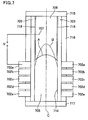
- Fig. 7 is a cross-sectional view illustrating the whole structure of an optical element (varifocal lens) which is one embodiment of the second electrowetting device of the present invention.
- a cylindrical side member 716, a translucent bottom member 717, and a translucent top member 715 are used as cell members.
- a cylindrical insulation layer 703 is disposed on the inner surface of the side member 716, and a surface layer 718 is disposed on the insulation layer 703 at the portion overlapping the upper portion of the side member 716.
- Ring-shaped electrodes 702a, 702b, 702c, 702d, and 702e are disposed on the exterior of the cylindrical insulation layer 703.
- a conductive liquid 706 is contained inside the cylindrical insulation layer 703, the conductive liquid being traversable therein.
- An electrode 707 is disposed opposite to the ring-shaped electrodes 702a, 702b, 702c, 702d, and 702e across the cylindrical insulator (inside the cylindrical insulation layer 703) and is in contact with the conductive liquid 706.
- One terminal of a power source V is connected with the electrode 707 by a conductor, while the other terminal is connected with the ring-shaped electrode 702a.
- a hydrophobic liquid 705 is contained inside the cylindrical insulation layer 703, the hydrophobic liquid being traversable therein.
- the hydrophobic liquid 705 is in contact with the insulation layer 703 at the portion overlapping the lower portion of the side member 716.
- the surface layer 718 preferably comprises a material having higher affinity (affinity force) for the conductive liquid 706 than for the hydrophobic liquid 705.
- the ring-shaped electrodes 702a, 702b, 702c, 702d, and 702e which are axially symmetric around the optical axis C, are disposed at different heights outside the insulation layer 703.
- the voltage supply V is connected only with the electrode 702a, but may appropriately be connected with any of the other electrodes 702b, 702c, 702d, and 702e so that the supply V can apply a voltage to a desired ring-shaped electrode.
- the state of the hydrophobic liquid 705 can continuously be changed from the state A to the state B.
- the cylindrical insulation layer 703 comprises the high dielectric film of the present invention, and may comprise the aforementioned high dielectric inorganic layer and water-repellent layer.
- the cylindrical insulation layer 703 may consist only of the high dielectric film of the present invention, may be a laminate comprising a high dielectric inorganic layer and the high dielectric film of the present invention disposed on the high dielectric inorganic layer, or may further comprise a water-repellent layer disposed on the high dielectric film of the present invention. Further, the cylindrical insulation layer 703 may be a laminate comprising the high dielectric film of the present invention and a water-repellent layer disposed on the high dielectric film.
- the laminate may comprise one or more high dielectric inorganic layers, one or more high dielectric films of the present invention, and one or more water-repellent layers.
- the conductive liquid, the hydrophobic liquid, the high dielectric inorganic layer, the water-repellent layer, the electrodes, and other components can be the same as those mentioned hereinabove with respect to the first electrowetting device of the present invention.
- the thickness of the film was measured using a digital length measuring system (MF-1001, Nikon Corp.).
- Aluminum was deposited in vacuo on each surface of the film, thereby preparing a sample.
- the capacitance and the dissipation factor of this sample were measured using an LCR meter (ZM2353, NF Corp.) at 30°C and 90°C and at a frequency of 1 kHz or 10 kHz under dry air atmosphere.
- the dielectric constant was calculated from the film thickness and the capacitance.
- volume resistivity ( ⁇ cm) was determined using a digital ultra megohmmeter/pico-ammeter at 90°C and at 300 V DC in dry air atmosphere.
- the voltage resistance of the film disposed on a substrate was determined using a hipot and insulation resistance tester (TOS9201, KIKUSUI ELECTRONICS CORP.) under dry air atmosphere. The measurement was performed at a voltage-increasing rate of 100 V/s.
- a heat-of-fusion curve was drawn using a differential scanning calorimetry (DSC) device at a temperature-increasing rate of 10°C/min, and the temperature corresponding to the local maximum of this curve was defined as the melting point.
- DSC differential scanning calorimetry
- the average primary particle size of the inorganic oxide particles was determined using a laser diffraction/scattering particle size distribution analyzer (trade name: LA-920, HORIBA, Ltd.).
- the fluoropolymer was subjected to a F-NMR measurement using a nuclear magnetic resonance device (type: VNS400MHz, manufacturer: Varian (the present Agilent Technologies Inc.), providing the spectrum. Based on the integral values of the respective peaks and the following formulas, the compositional ratio was determined.
- the ratio of the ⁇ -crystal structure was determined as follows. Specifically, the absorbance of the absorption peak (839 cm -1 ) assigned to the ⁇ -crystal and the absorbance of the absorption peak (763 cm -1 ) assigned to the ⁇ -crystal were determined using a Fourier transform infrared (FT-IR) spectrophotometer (trade name: spectrum One, Perkin Elmer Inc.). The ratios of the respective absorbances were defined as the ratios of the respective crystallinities. Then, the ratio of the ( ⁇ -crystal structure was calculated from the following formulas.
- FT-IR Fourier transform infrared
- the ratio is a value calculated on the basis of the results of the FT-IR measurement and the following formulas.
- the total light transmittance was determined using HAZE-GARD II (trade name, Toyo Seiki Seisaku-sho, Ltd.) in conformity with ASTM D1003.
- the total haze value was measured using HAZE-GARD II (trade name, Toyo Seiki Seisaku-sho, Ltd.) in conformity with ASTM D1003.
- the internal haze value was measured in the same manner as in the measurement of the total haze value except that the film is put into water contained in a glass cell.
- the external haze value was calculated by subtracting the internal haze value from the total haze value of the film.
- the rate of change in electromechanical coupling coefficient (kt value) was defined as the coefficient of variation of thickness of the film.
- the electromechanical coupling coefficient (kt value) was calculated as follows. Specifically, an Al-deposited electrode was formed on each surface of a piezoelectric film. A 13-mm-diameter disc was cut out of a predetermined part of the piezoelectric film, and the kt value of this disc was determined using an impedance analyzer (4194A, Hewlett-Packard Co.) by the method of H. Ohigashi et al., "The application of ferroelectric polymer, Ultrasonic transducers in the megahertz range ".
- the rate of change in electromechanical coupling coefficient was determined by:
- TFE tetrafluoroethylene
- VdF vinylene fluoride
- TFE tetrafluoroethylene
- VdF vinylene fluoride
- TFE tetrafluoroethylene
- VdF vinylene fluoride
- the components were stirred with a stirrer, thereby providing a 20 w/w% fluororesin solution.
- This fluororesin solution was casted on a polyethylene terephthalate (PET) film, which was a 38- ⁇ m-thick release-treated nonporous polyester film, using a gravure coater in a class 1000 cleanroom.
- the workpiece was dried through drying furnaces (2 m each, 10 m in total) at 80°C, 120°C, 175°C, 175°C, and 175°C at a rate of 7.5 m/min for 1.3 minutes, thereby providing a laminate film including a PET film and a fluororesin film. Then, the fluororesin film was peeled off the PET film, providing a 4.1- ⁇ m-thick film.
- the ratio of the ⁇ -crystal structure was 0% and the ratio of the ⁇ -crystal structure was 100%.
- the components were stirred with a stirrer, thereby providing a 20 w/w% fluororesin solution.
- This fluororesin solution was applied to a polyethylene terephthalate (PET) film, which was a 38- ⁇ m-thick release-treated nonporous polyester film, using a gravure coater in a class 1000 cleanroom.
- PET polyethylene terephthalate
- the workpiece was dried through drying furnaces (2 m each, 10 m in total) at 80°C, 120°C, 175°C, 175°C, and 175°C at a rate of 7.5 m/min for 1.3 minutes, thereby providing a laminate film including a PET film and a fluororesin film. Then, the fluororesin film was peeled off the PET film, providing a 4.2- ⁇ m-thick film.
- the ratio of the ⁇ -crystal structure was 0% and the ratio of the ⁇ -crystal structure was 100%.
- a film was produced in the same manner as in Example 2 except that the amount of ⁇ -Al 2 O 3 was as shown in Table 1.
- the ratio of the ⁇ -crystal structure was 0% and the ratio of the ⁇ -crystal structure was 100%.
- the ratio of the ⁇ -crystal structure was 0% and the ratio of the ( ⁇ -crystal structure was 100%.
- the ratio of the ⁇ -crystal structure was 0% and the ratio of the ⁇ -crystal structure was 100%.
- Example 6 the ratio of the ⁇ -crystal structure was 0% and the ratio of the ⁇ -crystal structure was 100%.
- a film was produced in the same manner as in Example 1 except that the VdF/TFE copolymer (a1) was replaced by polyvinylidene fluoride (trade name: VP825, DAIKIN INDUSTRIES, Ltd., melting point: 170°C).
- VdF/TFE copolymer (a1) was replaced by polyvinylidene fluoride (trade name: VP825, DAIKIN INDUSTRIES, Ltd., melting point: 170°C).
- a film was produced in the same manner as in Example 1 except that the temperatures of the respective drying furnaces were 80°C, 120°C, 140°C, 140°C, and 140°C.
- the ratio of the ⁇ -crystal structure was 61.3% and the ratio of the ⁇ -crystal structure was 38.7%.
- a film was produced in the same manner as in Example 2 except that ⁇ -Al 2 O 3 (trade name: AKP-G15, Sumitomo Chemical Co., Ltd., average primary particle size: 100 nm) was replaced by ⁇ -Al 2 O 3 (trade name: AKP-30, Sumitomo Chemical Co., Ltd., average primary particle size: 300 nm) and the amount thereof was as shown in the following Table 2.
- ⁇ -Al 2 O 3 trade name: AKP-G15, Sumitomo Chemical Co., Ltd., average primary particle size: 100 nm
- ⁇ -Al 2 O 3 trade name: AKP-30, Sumitomo Chemical Co., Ltd., average primary particle size: 300 nm
- a film was produced in the same manner as in Example 2 except that ⁇ -Al 2 O 3 (trade name: AKP-G15, Sumitomo Chemical Co., Ltd., average primary particle size: 100 nm) was replaced by MgO (trade name: 3310FY, ATR, average primary particle size: 30 nm) and the amount thereof was as shown in the following Table 2.
- ⁇ -Al 2 O 3 trade name: AKP-G15, Sumitomo Chemical Co., Ltd., average primary particle size: 100 nm
- MgO trade name: 3310FY, ATR, average primary particle size: 30 nm
- a film was produced in the same manner as in Example 2 except that ⁇ -Al 2 O 3 (trade name: AKP-G15, Sumitomo Chemical Co., Ltd., average primary particle size: 100 nm) was replaced by MgO ⁇ Al 2 O 3 (trade name: TSP-20, TAIMEI CHEMICALS CO., LTD., average primary particle size: 240 nm) and the amount thereof was as shown in the following Table 2.
- the ratio of the ⁇ -crystal structure was 0% and the ratio of the ( ⁇ -crystal structure was 100%.
- a film was produced in the same manner as in Example 2 except that ⁇ -Al 2 O 3 (trade name: AKP-G15, Sumitomo Chemical Co., Ltd., average primary particle size: 100 nm) was replaced by BaTiO 3 (trade name: T-BTO-50RF, TODA KOGYO CORP., average primary particle size: 50 nm) and the amount thereof was as shown in the following Table 2.
- ⁇ -Al 2 O 3 trade name: AKP-G15, Sumitomo Chemical Co., Ltd., average primary particle size: 100 nm
- BaTiO 3 trade name: T-BTO-50RF, TODA KOGYO CORP., average primary particle size: 50 nm
- the ratio of the ⁇ -crystal structure was 0% and the ratio of the ⁇ -crystal structure was 100%.
- a film was produced in the same manner as in Example 2 except that ⁇ -Al 2 O 3 (trade name: AKP-G15, Sumitomo Chemical Co., Ltd., average primary particle size: 100 nm) was replaced by 3Al 2 O 3 ⁇ 2SiO 2 (trade name: High-Purity Mullite, KCM Corp., average primary particle size: 700 nm) and the amount thereof was as shown in the following Table 2.
- ⁇ -Al 2 O 3 trade name: AKP-G15, Sumitomo Chemical Co., Ltd., average primary particle size: 100 nm
- 3Al 2 O 3 ⁇ 2SiO 2 trade name: High-Purity Mullite, KCM Corp., average primary particle size: 700 nm
- Example 7 8 9 10 11 (A) Film-forming resin (parts by mass) VdF/TFE (93/7 mol%) 200 200 200 200 200 (B) Inorganic oxide particles (parts by mass) ⁇ -Al 2 O 3 10 - - - - MgO - 10 - - - MgO ⁇ Al 2 O 3 - - 10 - - BaTiO 3 - - - 10 - 3Al 2 O 3 ⁇ 2SiO 2 - - - - 10 Average primary particle size (nm) 300 30 240 50 700 (B)/(A) (ratio by mass) 5/100 5/100 5/100 5/100 5/100 5/100 Film properties Thickness ( ⁇ m) 4.1 4.0 4.2 3.9 4.1 Volume resistivity ( ⁇ cm) 3.7 ⁇ 10 14 2.4 ⁇ 10 14 2.1 ⁇ 10 14 1.9 ⁇ 10 14 3.2 ⁇ 10 14 Voltage resistance (V/ ⁇ m) 670 510 510
- the ratio of the ⁇ -crystal structure was 0% and the ratio of the ⁇ -crystal structure was 100%.
- the ratio of the ⁇ -crystal structure was 0% and the ratio of the ⁇ -crystal structure was 100%.
- a film was produced in the same manner as in Example 1 except that the temperatures of the respective drying furnaces were 80°C, 120°C, 160°C, 160°C, and 160°C.
- the ratio of the ⁇ -crystal structure was 29.0% and the ratio of the ( ⁇ -crystal structure was 71.0%.
- a film was produced in the same manner as in Example 1 except that the temperatures of the respective drying furnaces were 80°C, 120°C, 165°C, 165°C, and 165°C.
- the ratio of the ⁇ -crystal structure was 25.4% and the ratio of the ⁇ -crystal structure was 74.6%.
- a film was produced in the same manner as in Example 1 except that the temperatures of the respective drying furnaces were 80°C, 120°C, 155°C, 155°C, and 155°C.
- the ratio of the ⁇ -crystal structure was 43.0% and the ratio of the ⁇ -crystal structure was 57.0%.
- a film was produced in the same manner as in Example 1 except that the temperatures of the respective drying furnaces were 80°C, 120°C, 150°C, 150°C, and 150°C.
- a film was produced in the same manner as in Example 1 except that the temperatures of the respective drying furnaces were as shown in the following Table 4.
- Table 4 shows the drying conditions and the corresponding ratios of the ⁇ -crystal structure and the ⁇ -crystal structure in the films produced in Example 1, Examples 14 to 18, Comparative Example 2, and Comparative Example 3.
- Drying at a temperature higher than the melting point can provide a film having a ratio of the ⁇ -crystal structure of 50% or more.
- drying at 175°C or higher can provide a film having a ratio of the ⁇ -crystal structure of 100%.
- drying the resin having the aforementioned composition in a drying condition higher than the melting point is an essential condition for producing a film having a high dielectric constant and a low dissipation factor.
- TFE/VdF 7/93
- MEK methyl ethyl ketone
- NMP N-methyl-2-pyrrolidone
- the coating was applied onto a PET film (by a casting technique) using a die coater and then dried, thereby providing a 3- ⁇ m-thick film.
- the drying furnace was divided into 5 zones (2 m each, 10 m in total), and the drying temperatures of the respective zones were 80°C, 120°C, 175°C, 175°C, and 175°C from the inlet side.
- the workpiece was passed through the drying furnace at a rate of 7.5 m/min for 1.3 minutes, thereby providing a laminate film comprising a PET film and a fluororesin film disposed on the PET film. Then, the fluororesin film was peeled off the PET film.
- the ratio of the ⁇ -crystal structure was 0% and the ratio of the ⁇ -crystal structure was 100%.
- the total light transmittance, the haze value, and the coefficient of variation of thickness of the film were determined.
- Table 5 shows the results.
- the resulting film was stuck on ITO-coated glass 80 ⁇ (Nippon Sheet Glass Co. Ltd.) using a roll press, and then annealed at 135°C for 12 hours to strengthen the sticking.
- DAIFREE GF500 (DAIKIN INDUSTRIES, Ltd.) was spin coated on the film to provide a water-repellent layer having a thickness of 0.1 ⁇ m.
- the electrowetting requires a high total light transmittance and a low haze value, as well as a large difference in contact angle of waterdrop before and after the voltage application.
- the coefficient of variation of thickness was low after the annealing, causing a large difference in contact angle of waterdrop before and after the voltage application.
- the high dielectric film of the present invention has a high dielectric constant and a low dissipation factor, and thus is suitable as a film for electrowetting.
Landscapes
- Chemical & Material Sciences (AREA)
- Physics & Mathematics (AREA)
- Engineering & Computer Science (AREA)
- Manufacturing & Machinery (AREA)
- Optics & Photonics (AREA)
- General Physics & Mathematics (AREA)
- Power Engineering (AREA)
- Chemical Kinetics & Catalysis (AREA)
- Organic Chemistry (AREA)
- Polymers & Plastics (AREA)
- Medicinal Chemistry (AREA)
- Health & Medical Sciences (AREA)
- Microelectronics & Electronic Packaging (AREA)
- Materials Engineering (AREA)
- Inorganic Chemistry (AREA)
- Electrochromic Elements, Electrophoresis, Or Variable Reflection Or Absorption Elements (AREA)
- Addition Polymer Or Copolymer, Post-Treatments, Or Chemical Modifications (AREA)
- Manufacture Of Macromolecular Shaped Articles (AREA)
- Compositions Of Macromolecular Compounds (AREA)
- Fixed Capacitors And Capacitor Manufacturing Machines (AREA)
- Mechanical Light Control Or Optical Switches (AREA)
- Laminated Bodies (AREA)
Applications Claiming Priority (3)
| Application Number | Priority Date | Filing Date | Title |
|---|---|---|---|
| JP2012228973 | 2012-10-16 | ||
| JP2013007606 | 2013-01-18 | ||
| PCT/JP2013/078073 WO2014061700A1 (fr) | 2012-10-16 | 2013-10-16 | Film à haute constante diélectrique |
Publications (3)
| Publication Number | Publication Date |
|---|---|
| EP2910604A1 true EP2910604A1 (fr) | 2015-08-26 |
| EP2910604A4 EP2910604A4 (fr) | 2016-06-15 |
| EP2910604B1 EP2910604B1 (fr) | 2022-04-13 |
Family
ID=50488261
Family Applications (1)
| Application Number | Title | Priority Date | Filing Date |
|---|---|---|---|
| EP13848067.8A Active EP2910604B1 (fr) | 2012-10-16 | 2013-10-16 | Film à haute constante diélectrique |
Country Status (6)
| Country | Link |
|---|---|
| US (1) | US20150368413A1 (fr) |
| EP (1) | EP2910604B1 (fr) |
| JP (2) | JP5516817B1 (fr) |
| CN (1) | CN104704046A (fr) |
| DK (1) | DK2910604T3 (fr) |
| WO (1) | WO2014061700A1 (fr) |
Cited By (1)
| Publication number | Priority date | Publication date | Assignee | Title |
|---|---|---|---|---|
| EP3778724A4 (fr) * | 2018-03-30 | 2021-12-29 | Hiroshima University | Article moulé |
Families Citing this family (20)
| Publication number | Priority date | Publication date | Assignee | Title |
|---|---|---|---|---|
| US20150025608A1 (en) | 2013-07-22 | 2015-01-22 | Cardiac Pacemakers, Inc. | Lubricious, biocompatible hydrophilic thermoset coating using interpenetrating hydrogel networks |
| JP6327334B2 (ja) * | 2014-02-26 | 2018-05-23 | ダイキン工業株式会社 | バイモルフ型圧電フィルム |
| US10745531B2 (en) * | 2015-07-17 | 2020-08-18 | Daikin Industries, Ltd. | Film |
| DE112016003327B4 (de) * | 2015-07-23 | 2022-08-18 | Sumitomo Bakelite Co., Ltd. | Substrat für Leistungsmodul, Leiterplatte für Leistungsmodul und Leistungsmodul |
| CN107847737B (zh) * | 2015-07-25 | 2021-03-02 | 心脏起搏器股份公司 | 具有生物稳定的pvdf基材料的医用电引线 |
| WO2017126374A1 (fr) * | 2016-01-18 | 2017-07-27 | シャープ株式会社 | Substrat d'électrode, son procédé de production et dispositif électronique |
| EP3428219A4 (fr) * | 2016-02-29 | 2020-02-19 | Toppan Printing Co., Ltd. | Film de résine à base de fluor, et procédé de production de film de résine à base de fluor |
| KR102041660B1 (ko) * | 2016-08-12 | 2019-11-06 | 주식회사 엘지화학 | 햅틱 디스플레이 필름용 분산액, 햅틱 디스플레이 필름 및 이의 제조방법 |
| EP3327067A1 (fr) * | 2016-11-23 | 2018-05-30 | Fundación BCMaterials - Basque Center for Materials, Application and Nanostructures | Procédé de fabrication d'un film constitué de fluorure de polyvinylidène et film constitué de polyvinylidène fluoride en phase bêta |
| JP6760404B2 (ja) * | 2017-01-31 | 2020-09-23 | ダイキン工業株式会社 | フッ素樹脂フィルム |
| CN111295413A (zh) * | 2017-11-08 | 2020-06-16 | 大金工业株式会社 | 膜 |
| JP7321145B2 (ja) * | 2018-03-30 | 2023-08-04 | ダイキン工業株式会社 | 成形体 |
| JP6899588B2 (ja) * | 2018-11-20 | 2021-07-07 | 国立研究開発法人産業技術総合研究所 | 液体操作装置 |
| CN109910403B (zh) * | 2019-04-12 | 2021-01-29 | 中国电子科技集团公司第三十八研究所 | 一种微波复合介质板的制备方法及制得的微波复合介质板 |
| EP4152091B1 (fr) * | 2020-05-29 | 2026-04-08 | Huawei Technologies Co., Ltd. | Ouverture pour liquide, dispositif électronique, et procédé et appareil de commande d'une ouverture pour liquide |
| US20240067783A1 (en) * | 2020-09-30 | 2024-02-29 | Junkosha Inc. | Fluororesin Film |
| CN116490548A (zh) * | 2020-09-30 | 2023-07-25 | 株式会社润工社 | 一种氟树脂膜 |
| KR102946083B1 (ko) * | 2020-12-18 | 2026-04-01 | 삼성전기주식회사 | 적층형 전자 부품 및 그 제조방법 |
| FR3128714A1 (fr) * | 2021-10-29 | 2023-05-05 | Arkema Inc. | Vdf contenant un (co)polymère ayant une grande masse moléculaire par utilisation d’un nouveau procédé de polymérisation par précipitation |
| US12408459B2 (en) * | 2021-11-30 | 2025-09-02 | Visera Technologies Company Limited | Image sensor having liquid-lens units and method for detecting images |
Family Cites Families (19)
| Publication number | Priority date | Publication date | Assignee | Title |
|---|---|---|---|---|
| JPS6040137A (ja) * | 1983-08-15 | 1985-03-02 | Kureha Chem Ind Co Ltd | フツ化ビニリデン共重合体フイルム |
| JPS6055034A (ja) * | 1983-09-06 | 1985-03-29 | Mitsubishi Petrochem Co Ltd | 高分子エレクトレツト素子の製造法 |
| US4711808A (en) * | 1986-02-19 | 1987-12-08 | Eastman Kodak Company | Beta phase PVF2 film formed by casting it onto a specially prepared insulating support |
| JPH0315005A (ja) * | 1989-03-10 | 1991-01-23 | Kureha Chem Ind Co Ltd | 光学位相差板及びその製造方法 |
| KR920007285B1 (ko) * | 1989-03-10 | 1992-08-29 | 구레하 가가꾸 고오교 가부시끼가이샤 | 광학 위상차판 및 그 제조 방법 |
| JPH05249315A (ja) * | 1992-03-04 | 1993-09-28 | Kureha Chem Ind Co Ltd | 光学位相差板及びその製造方法 |
| JPH06342947A (ja) * | 1993-06-01 | 1994-12-13 | Kureha Chem Ind Co Ltd | 多孔質圧電体の製造方法及びポリマ−圧電性多孔膜 |
| JPH0737755A (ja) * | 1993-07-16 | 1995-02-07 | Murata Mfg Co Ltd | 誘電体薄膜素子 |
| JP4391142B2 (ja) * | 2003-06-25 | 2009-12-24 | 株式会社クレハ | 半導電性樹脂組成物、その製造方法、半導電性シート、及び電荷制御部材 |
| US7048889B2 (en) * | 2004-03-23 | 2006-05-23 | Lucent Technologies Inc. | Dynamically controllable biological/chemical detectors having nanostructured surfaces |
| EP1792919B1 (fr) * | 2004-08-06 | 2014-11-12 | Daikin Industries, Ltd. | Procédé pour produire un fluorure de vinylidène d'homopolymère ayant une structure de cristal de type i et film fin |
| JP4845084B2 (ja) * | 2005-02-28 | 2011-12-28 | 独立行政法人産業技術総合研究所 | 強誘電体フィルム及びその製造方法 |
| JP4894703B2 (ja) | 2006-09-29 | 2012-03-14 | ソニー株式会社 | エレクトロウエッティング装置とこれを用いた可変焦点レンズ、光ピックアップ装置、光記録再生装置、液滴操作装置、光学素子、ズームレンズ、撮像装置、光変調装置及び表示装置 |
| JP5467771B2 (ja) * | 2007-01-26 | 2014-04-09 | ダイキン工業株式会社 | 高耐電圧を有する高誘電体フィルム |
| JP5070976B2 (ja) * | 2007-07-31 | 2012-11-14 | ダイキン工業株式会社 | 高誘電性フィルム |
| JP4936026B2 (ja) * | 2009-04-02 | 2012-05-23 | 宇部興産株式会社 | 導電性バインダーの製造方法 |
| KR20120123432A (ko) * | 2010-01-20 | 2012-11-08 | 다이킨 고교 가부시키가이샤 | 고유전성 필름 |
| JP2012181513A (ja) * | 2011-02-10 | 2012-09-20 | Daikin Ind Ltd | エレクトロウエッティング用疎水性誘電体フィルム |
| KR20140026604A (ko) * | 2011-06-15 | 2014-03-05 | 가부시끼가이샤 구레하 | 폴리불화비닐리덴 수지 필름, 다층 필름, 및 태양 전지 모듈용 백 시트, 및 필름의 제조 방법 |
-
2013
- 2013-10-16 EP EP13848067.8A patent/EP2910604B1/fr active Active
- 2013-10-16 US US14/433,685 patent/US20150368413A1/en not_active Abandoned
- 2013-10-16 DK DK13848067.8T patent/DK2910604T3/da active
- 2013-10-16 WO PCT/JP2013/078073 patent/WO2014061700A1/fr not_active Ceased
- 2013-10-16 CN CN201380051473.8A patent/CN104704046A/zh active Pending
- 2013-10-16 JP JP2013215427A patent/JP5516817B1/ja active Active
-
2014
- 2014-01-31 JP JP2014016868A patent/JP5804100B2/ja active Active
Cited By (1)
| Publication number | Priority date | Publication date | Assignee | Title |
|---|---|---|---|---|
| EP3778724A4 (fr) * | 2018-03-30 | 2021-12-29 | Hiroshima University | Article moulé |
Also Published As
| Publication number | Publication date |
|---|---|
| JP5804100B2 (ja) | 2015-11-04 |
| JP2014156599A (ja) | 2014-08-28 |
| EP2910604B1 (fr) | 2022-04-13 |
| DK2910604T3 (da) | 2022-05-16 |
| JP2014156581A (ja) | 2014-08-28 |
| WO2014061700A1 (fr) | 2014-04-24 |
| US20150368413A1 (en) | 2015-12-24 |
| EP2910604A4 (fr) | 2016-06-15 |
| CN104704046A (zh) | 2015-06-10 |
| JP5516817B1 (ja) | 2014-06-11 |
Similar Documents
| Publication | Publication Date | Title |
|---|---|---|
| EP2910604B1 (fr) | Film à haute constante diélectrique | |
| EP2674804A1 (fr) | Film diélectrique hydrophobe pour électromouillage | |
| TWI760200B (zh) | 以dc不均衡波形驅動電泳顯示器之方法 | |
| EP3064537B1 (fr) | Film et son procédé de production | |
| JP6547627B2 (ja) | 圧電フィルム | |
| EP3508519B1 (fr) | Film | |
| JP5135937B2 (ja) | 高誘電性フィルム | |
| KR20180030144A (ko) | 필름 | |
| JP5070976B2 (ja) | 高誘電性フィルム | |
| JP6468441B2 (ja) | 圧電フィルム | |
| US20150332855A1 (en) | Multilayer film | |
| WO2015053344A1 (fr) | Film piézoélectrique | |
| KR101674081B1 (ko) | 고유전성 필름컨덴서용 조성물, 이의 제조방법 및 이를 포함하는 필름컨덴서용 고유전성 필름 | |
| JP2015088566A (ja) | 圧電フィルム及びその製造方法 | |
| JP6520714B2 (ja) | フィルム | |
| US20090014319A1 (en) | Transparent insulating film, method for producing the same, and sputtering target | |
| JP2015110717A (ja) | フィルム |
Legal Events
| Date | Code | Title | Description |
|---|---|---|---|
| PUAI | Public reference made under article 153(3) epc to a published international application that has entered the european phase |
Free format text: ORIGINAL CODE: 0009012 |
|
| 17P | Request for examination filed |
Effective date: 20150423 |
|
| AK | Designated contracting states |
Kind code of ref document: A1 Designated state(s): AL AT BE BG CH CY CZ DE DK EE ES FI FR GB GR HR HU IE IS IT LI LT LU LV MC MK MT NL NO PL PT RO RS SE SI SK SM TR |
|
| AX | Request for extension of the european patent |
Extension state: BA ME |
|
| DAX | Request for extension of the european patent (deleted) | ||
| RA4 | Supplementary search report drawn up and despatched (corrected) |
Effective date: 20160519 |
|
| RIC1 | Information provided on ipc code assigned before grant |
Ipc: C08K 3/20 20060101ALI20160512BHEP Ipc: G02F 1/19 20060101ALI20160512BHEP Ipc: G02B 26/00 20060101ALI20160512BHEP Ipc: H01G 4/18 20060101ALI20160512BHEP Ipc: G02B 3/14 20060101ALI20160512BHEP Ipc: C08L 27/16 20060101AFI20160512BHEP Ipc: G02B 26/02 20060101ALI20160512BHEP Ipc: C08J 5/18 20060101ALI20160512BHEP |
|
| STAA | Information on the status of an ep patent application or granted ep patent |
Free format text: STATUS: EXAMINATION IS IN PROGRESS |
|
| 17Q | First examination report despatched |
Effective date: 20181018 |
|
| GRAP | Despatch of communication of intention to grant a patent |
Free format text: ORIGINAL CODE: EPIDOSNIGR1 |
|
| STAA | Information on the status of an ep patent application or granted ep patent |
Free format text: STATUS: GRANT OF PATENT IS INTENDED |
|
| INTG | Intention to grant announced |
Effective date: 20211208 |
|
| GRAS | Grant fee paid |
Free format text: ORIGINAL CODE: EPIDOSNIGR3 |
|
| GRAA | (expected) grant |
Free format text: ORIGINAL CODE: 0009210 |
|
| STAA | Information on the status of an ep patent application or granted ep patent |
Free format text: STATUS: THE PATENT HAS BEEN GRANTED |
|
| AK | Designated contracting states |
Kind code of ref document: B1 Designated state(s): AL AT BE BG CH CY CZ DE DK EE ES FI FR GB GR HR HU IE IS IT LI LT LU LV MC MK MT NL NO PL PT RO RS SE SI SK SM TR |
|
| REG | Reference to a national code |
Ref country code: GB Ref legal event code: FG4D |
|
| REG | Reference to a national code |
Ref country code: CH Ref legal event code: EP |
|
| REG | Reference to a national code |
Ref country code: DE Ref legal event code: R096 Ref document number: 602013081415 Country of ref document: DE |
|
| REG | Reference to a national code |
Ref country code: IE Ref legal event code: FG4D |
|
| REG | Reference to a national code |
Ref country code: AT Ref legal event code: REF Ref document number: 1483408 Country of ref document: AT Kind code of ref document: T Effective date: 20220515 |
|
| REG | Reference to a national code |
Ref country code: DK Ref legal event code: T3 Effective date: 20220512 |
|
| REG | Reference to a national code |
Ref country code: LT Ref legal event code: MG9D |
|
| REG | Reference to a national code |
Ref country code: NL Ref legal event code: MP Effective date: 20220413 |
|
| REG | Reference to a national code |
Ref country code: AT Ref legal event code: MK05 Ref document number: 1483408 Country of ref document: AT Kind code of ref document: T Effective date: 20220413 |
|
| PG25 | Lapsed in a contracting state [announced via postgrant information from national office to epo] |
Ref country code: NL Free format text: LAPSE BECAUSE OF FAILURE TO SUBMIT A TRANSLATION OF THE DESCRIPTION OR TO PAY THE FEE WITHIN THE PRESCRIBED TIME-LIMIT Effective date: 20220413 |
|
| PG25 | Lapsed in a contracting state [announced via postgrant information from national office to epo] |
Ref country code: SE Free format text: LAPSE BECAUSE OF FAILURE TO SUBMIT A TRANSLATION OF THE DESCRIPTION OR TO PAY THE FEE WITHIN THE PRESCRIBED TIME-LIMIT Effective date: 20220413 Ref country code: PT Free format text: LAPSE BECAUSE OF FAILURE TO SUBMIT A TRANSLATION OF THE DESCRIPTION OR TO PAY THE FEE WITHIN THE PRESCRIBED TIME-LIMIT Effective date: 20220816 Ref country code: NO Free format text: LAPSE BECAUSE OF FAILURE TO SUBMIT A TRANSLATION OF THE DESCRIPTION OR TO PAY THE FEE WITHIN THE PRESCRIBED TIME-LIMIT Effective date: 20220713 Ref country code: LT Free format text: LAPSE BECAUSE OF FAILURE TO SUBMIT A TRANSLATION OF THE DESCRIPTION OR TO PAY THE FEE WITHIN THE PRESCRIBED TIME-LIMIT Effective date: 20220413 Ref country code: HR Free format text: LAPSE BECAUSE OF FAILURE TO SUBMIT A TRANSLATION OF THE DESCRIPTION OR TO PAY THE FEE WITHIN THE PRESCRIBED TIME-LIMIT Effective date: 20220413 Ref country code: GR Free format text: LAPSE BECAUSE OF FAILURE TO SUBMIT A TRANSLATION OF THE DESCRIPTION OR TO PAY THE FEE WITHIN THE PRESCRIBED TIME-LIMIT Effective date: 20220714 Ref country code: FI Free format text: LAPSE BECAUSE OF FAILURE TO SUBMIT A TRANSLATION OF THE DESCRIPTION OR TO PAY THE FEE WITHIN THE PRESCRIBED TIME-LIMIT Effective date: 20220413 Ref country code: ES Free format text: LAPSE BECAUSE OF FAILURE TO SUBMIT A TRANSLATION OF THE DESCRIPTION OR TO PAY THE FEE WITHIN THE PRESCRIBED TIME-LIMIT Effective date: 20220413 Ref country code: BG Free format text: LAPSE BECAUSE OF FAILURE TO SUBMIT A TRANSLATION OF THE DESCRIPTION OR TO PAY THE FEE WITHIN THE PRESCRIBED TIME-LIMIT Effective date: 20220713 Ref country code: AT Free format text: LAPSE BECAUSE OF FAILURE TO SUBMIT A TRANSLATION OF THE DESCRIPTION OR TO PAY THE FEE WITHIN THE PRESCRIBED TIME-LIMIT Effective date: 20220413 |
|
| PG25 | Lapsed in a contracting state [announced via postgrant information from national office to epo] |
Ref country code: RS Free format text: LAPSE BECAUSE OF FAILURE TO SUBMIT A TRANSLATION OF THE DESCRIPTION OR TO PAY THE FEE WITHIN THE PRESCRIBED TIME-LIMIT Effective date: 20220413 Ref country code: PL Free format text: LAPSE BECAUSE OF FAILURE TO SUBMIT A TRANSLATION OF THE DESCRIPTION OR TO PAY THE FEE WITHIN THE PRESCRIBED TIME-LIMIT Effective date: 20220413 Ref country code: LV Free format text: LAPSE BECAUSE OF FAILURE TO SUBMIT A TRANSLATION OF THE DESCRIPTION OR TO PAY THE FEE WITHIN THE PRESCRIBED TIME-LIMIT Effective date: 20220413 Ref country code: IS Free format text: LAPSE BECAUSE OF FAILURE TO SUBMIT A TRANSLATION OF THE DESCRIPTION OR TO PAY THE FEE WITHIN THE PRESCRIBED TIME-LIMIT Effective date: 20220813 |
|
| REG | Reference to a national code |
Ref country code: DE Ref legal event code: R097 Ref document number: 602013081415 Country of ref document: DE |
|
| PG25 | Lapsed in a contracting state [announced via postgrant information from national office to epo] |
Ref country code: SM Free format text: LAPSE BECAUSE OF FAILURE TO SUBMIT A TRANSLATION OF THE DESCRIPTION OR TO PAY THE FEE WITHIN THE PRESCRIBED TIME-LIMIT Effective date: 20220413 Ref country code: SK Free format text: LAPSE BECAUSE OF FAILURE TO SUBMIT A TRANSLATION OF THE DESCRIPTION OR TO PAY THE FEE WITHIN THE PRESCRIBED TIME-LIMIT Effective date: 20220413 Ref country code: RO Free format text: LAPSE BECAUSE OF FAILURE TO SUBMIT A TRANSLATION OF THE DESCRIPTION OR TO PAY THE FEE WITHIN THE PRESCRIBED TIME-LIMIT Effective date: 20220413 Ref country code: EE Free format text: LAPSE BECAUSE OF FAILURE TO SUBMIT A TRANSLATION OF THE DESCRIPTION OR TO PAY THE FEE WITHIN THE PRESCRIBED TIME-LIMIT Effective date: 20220413 Ref country code: CZ Free format text: LAPSE BECAUSE OF FAILURE TO SUBMIT A TRANSLATION OF THE DESCRIPTION OR TO PAY THE FEE WITHIN THE PRESCRIBED TIME-LIMIT Effective date: 20220413 |
|
| PLBE | No opposition filed within time limit |
Free format text: ORIGINAL CODE: 0009261 |
|
| STAA | Information on the status of an ep patent application or granted ep patent |
Free format text: STATUS: NO OPPOSITION FILED WITHIN TIME LIMIT |
|
| 26N | No opposition filed |
Effective date: 20230116 |
|
| PG25 | Lapsed in a contracting state [announced via postgrant information from national office to epo] |
Ref country code: AL Free format text: LAPSE BECAUSE OF FAILURE TO SUBMIT A TRANSLATION OF THE DESCRIPTION OR TO PAY THE FEE WITHIN THE PRESCRIBED TIME-LIMIT Effective date: 20220413 |
|
| PG25 | Lapsed in a contracting state [announced via postgrant information from national office to epo] |
Ref country code: SI Free format text: LAPSE BECAUSE OF FAILURE TO SUBMIT A TRANSLATION OF THE DESCRIPTION OR TO PAY THE FEE WITHIN THE PRESCRIBED TIME-LIMIT Effective date: 20220413 Ref country code: MC Free format text: LAPSE BECAUSE OF FAILURE TO SUBMIT A TRANSLATION OF THE DESCRIPTION OR TO PAY THE FEE WITHIN THE PRESCRIBED TIME-LIMIT Effective date: 20220413 |
|
| REG | Reference to a national code |
Ref country code: CH Ref legal event code: PL |
|
| REG | Reference to a national code |
Ref country code: BE Ref legal event code: MM Effective date: 20221031 |
|
| PG25 | Lapsed in a contracting state [announced via postgrant information from national office to epo] |
Ref country code: LU Free format text: LAPSE BECAUSE OF NON-PAYMENT OF DUE FEES Effective date: 20221016 |
|
| P01 | Opt-out of the competence of the unified patent court (upc) registered |
Effective date: 20230525 |
|
| PG25 | Lapsed in a contracting state [announced via postgrant information from national office to epo] |
Ref country code: LI Free format text: LAPSE BECAUSE OF NON-PAYMENT OF DUE FEES Effective date: 20221031 Ref country code: CH Free format text: LAPSE BECAUSE OF NON-PAYMENT OF DUE FEES Effective date: 20221031 |
|
| PG25 | Lapsed in a contracting state [announced via postgrant information from national office to epo] |
Ref country code: BE Free format text: LAPSE BECAUSE OF NON-PAYMENT OF DUE FEES Effective date: 20221031 |
|
| PG25 | Lapsed in a contracting state [announced via postgrant information from national office to epo] |
Ref country code: IE Free format text: LAPSE BECAUSE OF NON-PAYMENT OF DUE FEES Effective date: 20221016 |
|
| PG25 | Lapsed in a contracting state [announced via postgrant information from national office to epo] |
Ref country code: HU Free format text: LAPSE BECAUSE OF FAILURE TO SUBMIT A TRANSLATION OF THE DESCRIPTION OR TO PAY THE FEE WITHIN THE PRESCRIBED TIME-LIMIT; INVALID AB INITIO Effective date: 20131016 |
|
| PG25 | Lapsed in a contracting state [announced via postgrant information from national office to epo] |
Ref country code: CY Free format text: LAPSE BECAUSE OF FAILURE TO SUBMIT A TRANSLATION OF THE DESCRIPTION OR TO PAY THE FEE WITHIN THE PRESCRIBED TIME-LIMIT Effective date: 20220413 |
|
| PG25 | Lapsed in a contracting state [announced via postgrant information from national office to epo] |
Ref country code: MK Free format text: LAPSE BECAUSE OF FAILURE TO SUBMIT A TRANSLATION OF THE DESCRIPTION OR TO PAY THE FEE WITHIN THE PRESCRIBED TIME-LIMIT Effective date: 20220413 |
|
| PG25 | Lapsed in a contracting state [announced via postgrant information from national office to epo] |
Ref country code: TR Free format text: LAPSE BECAUSE OF FAILURE TO SUBMIT A TRANSLATION OF THE DESCRIPTION OR TO PAY THE FEE WITHIN THE PRESCRIBED TIME-LIMIT Effective date: 20220413 |
|
| PG25 | Lapsed in a contracting state [announced via postgrant information from national office to epo] |
Ref country code: MT Free format text: LAPSE BECAUSE OF FAILURE TO SUBMIT A TRANSLATION OF THE DESCRIPTION OR TO PAY THE FEE WITHIN THE PRESCRIBED TIME-LIMIT Effective date: 20220413 |
|
| PG25 | Lapsed in a contracting state [announced via postgrant information from national office to epo] |
Ref country code: BG Free format text: LAPSE BECAUSE OF FAILURE TO SUBMIT A TRANSLATION OF THE DESCRIPTION OR TO PAY THE FEE WITHIN THE PRESCRIBED TIME-LIMIT Effective date: 20220413 |
|
| PG25 | Lapsed in a contracting state [announced via postgrant information from national office to epo] |
Ref country code: BG Free format text: LAPSE BECAUSE OF FAILURE TO SUBMIT A TRANSLATION OF THE DESCRIPTION OR TO PAY THE FEE WITHIN THE PRESCRIBED TIME-LIMIT Effective date: 20220413 |
|
| PGFP | Annual fee paid to national office [announced via postgrant information from national office to epo] |
Ref country code: IT Payment date: 20250922 Year of fee payment: 13 |
|
| PGFP | Annual fee paid to national office [announced via postgrant information from national office to epo] |
Ref country code: GB Payment date: 20250828 Year of fee payment: 13 |
|
| PGFP | Annual fee paid to national office [announced via postgrant information from national office to epo] |
Ref country code: FR Payment date: 20250908 Year of fee payment: 13 |
|
| PGFP | Annual fee paid to national office [announced via postgrant information from national office to epo] |
Ref country code: DE Payment date: 20250902 Year of fee payment: 13 |
|
| PGFP | Annual fee paid to national office [announced via postgrant information from national office to epo] |
Ref country code: DK Payment date: 20251014 Year of fee payment: 13 |