EP2930758A1 - Système de formation d'une couche mince de phosphore pour dispositifs électroluminescents à conversion au phosphore - Google Patents
Système de formation d'une couche mince de phosphore pour dispositifs électroluminescents à conversion au phosphore Download PDFInfo
- Publication number
- EP2930758A1 EP2930758A1 EP15167769.7A EP15167769A EP2930758A1 EP 2930758 A1 EP2930758 A1 EP 2930758A1 EP 15167769 A EP15167769 A EP 15167769A EP 2930758 A1 EP2930758 A1 EP 2930758A1
- Authority
- EP
- European Patent Office
- Prior art keywords
- phosphor
- phosphor powder
- subsystem
- deposition
- layer
- Prior art date
- Legal status (The legal status is an assumption and is not a legal conclusion. Google has not performed a legal analysis and makes no representation as to the accuracy of the status listed.)
- Granted
Links
Images


Classifications
-
- C—CHEMISTRY; METALLURGY
- C09—DYES; PAINTS; POLISHES; NATURAL RESINS; ADHESIVES; COMPOSITIONS NOT OTHERWISE PROVIDED FOR; APPLICATIONS OF MATERIALS NOT OTHERWISE PROVIDED FOR
- C09K—MATERIALS FOR MISCELLANEOUS APPLICATIONS, NOT PROVIDED FOR ELSEWHERE
- C09K11/00—Luminescent materials, e.g. electroluminescent or chemiluminescent
- C09K11/02—Use of particular materials as binders, particle coatings or suspension media therefor
- C09K11/025—Use of particular materials as binders, particle coatings or suspension media therefor non-luminescent particle coatings or suspension media
-
- H—ELECTRICITY
- H10—SEMICONDUCTOR DEVICES; ELECTRIC SOLID-STATE DEVICES NOT OTHERWISE PROVIDED FOR
- H10H—INORGANIC LIGHT-EMITTING SEMICONDUCTOR DEVICES HAVING POTENTIAL BARRIERS
- H10H20/00—Individual inorganic light-emitting semiconductor devices having potential barriers, e.g. light-emitting diodes [LED]
- H10H20/80—Constructional details
- H10H20/85—Packages
- H10H20/851—Wavelength conversion means
- H10H20/8514—Wavelength conversion means characterised by their shape, e.g. plate or foil
-
- C—CHEMISTRY; METALLURGY
- C23—COATING METALLIC MATERIAL; COATING MATERIAL WITH METALLIC MATERIAL; CHEMICAL SURFACE TREATMENT; DIFFUSION TREATMENT OF METALLIC MATERIAL; COATING BY VACUUM EVAPORATION, BY SPUTTERING, BY ION IMPLANTATION OR BY CHEMICAL VAPOUR DEPOSITION, IN GENERAL; INHIBITING CORROSION OF METALLIC MATERIAL OR INCRUSTATION IN GENERAL
- C23C—COATING METALLIC MATERIAL; COATING MATERIAL WITH METALLIC MATERIAL; SURFACE TREATMENT OF METALLIC MATERIAL BY DIFFUSION INTO THE SURFACE, BY CHEMICAL CONVERSION OR SUBSTITUTION; COATING BY VACUUM EVAPORATION, BY SPUTTERING, BY ION IMPLANTATION OR BY CHEMICAL VAPOUR DEPOSITION, IN GENERAL
- C23C16/00—Chemical coating by decomposition of gaseous compounds, without leaving reaction products of surface material in the coating, i.e. chemical vapour deposition [CVD] processes
- C23C16/44—Chemical coating by decomposition of gaseous compounds, without leaving reaction products of surface material in the coating, i.e. chemical vapour deposition [CVD] processes characterised by the method of coating
- C23C16/52—Controlling or regulating the coating process
-
- C—CHEMISTRY; METALLURGY
- C09—DYES; PAINTS; POLISHES; NATURAL RESINS; ADHESIVES; COMPOSITIONS NOT OTHERWISE PROVIDED FOR; APPLICATIONS OF MATERIALS NOT OTHERWISE PROVIDED FOR
- C09K—MATERIALS FOR MISCELLANEOUS APPLICATIONS, NOT PROVIDED FOR ELSEWHERE
- C09K11/00—Luminescent materials, e.g. electroluminescent or chemiluminescent
- C09K11/08—Luminescent materials, e.g. electroluminescent or chemiluminescent containing inorganic luminescent materials
-
- C—CHEMISTRY; METALLURGY
- C23—COATING METALLIC MATERIAL; COATING MATERIAL WITH METALLIC MATERIAL; CHEMICAL SURFACE TREATMENT; DIFFUSION TREATMENT OF METALLIC MATERIAL; COATING BY VACUUM EVAPORATION, BY SPUTTERING, BY ION IMPLANTATION OR BY CHEMICAL VAPOUR DEPOSITION, IN GENERAL; INHIBITING CORROSION OF METALLIC MATERIAL OR INCRUSTATION IN GENERAL
- C23C—COATING METALLIC MATERIAL; COATING MATERIAL WITH METALLIC MATERIAL; SURFACE TREATMENT OF METALLIC MATERIAL BY DIFFUSION INTO THE SURFACE, BY CHEMICAL CONVERSION OR SUBSTITUTION; COATING BY VACUUM EVAPORATION, BY SPUTTERING, BY ION IMPLANTATION OR BY CHEMICAL VAPOUR DEPOSITION, IN GENERAL
- C23C16/00—Chemical coating by decomposition of gaseous compounds, without leaving reaction products of surface material in the coating, i.e. chemical vapour deposition [CVD] processes
- C23C16/44—Chemical coating by decomposition of gaseous compounds, without leaving reaction products of surface material in the coating, i.e. chemical vapour deposition [CVD] processes characterised by the method of coating
- C23C16/455—Chemical coating by decomposition of gaseous compounds, without leaving reaction products of surface material in the coating, i.e. chemical vapour deposition [CVD] processes characterised by the method of coating characterised by the method used for introducing gases into reaction chamber or for modifying gas flows in reaction chamber
- C23C16/45563—Gas nozzles
- C23C16/45565—Shower nozzles
-
- C—CHEMISTRY; METALLURGY
- C23—COATING METALLIC MATERIAL; COATING MATERIAL WITH METALLIC MATERIAL; CHEMICAL SURFACE TREATMENT; DIFFUSION TREATMENT OF METALLIC MATERIAL; COATING BY VACUUM EVAPORATION, BY SPUTTERING, BY ION IMPLANTATION OR BY CHEMICAL VAPOUR DEPOSITION, IN GENERAL; INHIBITING CORROSION OF METALLIC MATERIAL OR INCRUSTATION IN GENERAL
- C23C—COATING METALLIC MATERIAL; COATING MATERIAL WITH METALLIC MATERIAL; SURFACE TREATMENT OF METALLIC MATERIAL BY DIFFUSION INTO THE SURFACE, BY CHEMICAL CONVERSION OR SUBSTITUTION; COATING BY VACUUM EVAPORATION, BY SPUTTERING, BY ION IMPLANTATION OR BY CHEMICAL VAPOUR DEPOSITION, IN GENERAL
- C23C16/00—Chemical coating by decomposition of gaseous compounds, without leaving reaction products of surface material in the coating, i.e. chemical vapour deposition [CVD] processes
- C23C16/44—Chemical coating by decomposition of gaseous compounds, without leaving reaction products of surface material in the coating, i.e. chemical vapour deposition [CVD] processes characterised by the method of coating
- C23C16/458—Chemical coating by decomposition of gaseous compounds, without leaving reaction products of surface material in the coating, i.e. chemical vapour deposition [CVD] processes characterised by the method of coating characterised by the method used for supporting substrates in the reaction chamber
- C23C16/4582—Rigid and flat substrates, e.g. plates or discs
- C23C16/4583—Rigid and flat substrates, e.g. plates or discs the substrate being supported substantially horizontally
- C23C16/4584—Rigid and flat substrates, e.g. plates or discs the substrate being supported substantially horizontally the substrate being rotated
-
- H—ELECTRICITY
- H01—ELECTRIC ELEMENTS
- H01J—ELECTRIC DISCHARGE TUBES OR DISCHARGE LAMPS
- H01J1/00—Details of electrodes, of magnetic control means, of screens, or of the mounting or spacing thereof, common to two or more basic types of discharge tubes or lamps
- H01J1/54—Screens on or from which an image or pattern is formed, picked-up, converted, or stored; Luminescent coatings on vessels
- H01J1/62—Luminescent screens; Selection of materials for luminescent coatings on vessels
- H01J1/64—Luminescent screens; Selection of materials for luminescent coatings on vessels characterised by the binder or adhesive for securing the luminescent material to its support
-
- H—ELECTRICITY
- H01—ELECTRIC ELEMENTS
- H01J—ELECTRIC DISCHARGE TUBES OR DISCHARGE LAMPS
- H01J1/00—Details of electrodes, of magnetic control means, of screens, or of the mounting or spacing thereof, common to two or more basic types of discharge tubes or lamps
- H01J1/54—Screens on or from which an image or pattern is formed, picked-up, converted, or stored; Luminescent coatings on vessels
- H01J1/62—Luminescent screens; Selection of materials for luminescent coatings on vessels
- H01J1/68—Luminescent screens; Selection of materials for luminescent coatings on vessels with superimposed luminescent layers
-
- H—ELECTRICITY
- H01—ELECTRIC ELEMENTS
- H01J—ELECTRIC DISCHARGE TUBES OR DISCHARGE LAMPS
- H01J1/00—Details of electrodes, of magnetic control means, of screens, or of the mounting or spacing thereof, common to two or more basic types of discharge tubes or lamps
- H01J1/54—Screens on or from which an image or pattern is formed, picked-up, converted, or stored; Luminescent coatings on vessels
- H01J1/62—Luminescent screens; Selection of materials for luminescent coatings on vessels
- H01J1/70—Luminescent screens; Selection of materials for luminescent coatings on vessels with protective, conductive, or reflective layers
-
- H—ELECTRICITY
- H05—ELECTRIC TECHNIQUES NOT OTHERWISE PROVIDED FOR
- H05B—ELECTRIC HEATING; ELECTRIC LIGHT SOURCES NOT OTHERWISE PROVIDED FOR; CIRCUIT ARRANGEMENTS FOR ELECTRIC LIGHT SOURCES, IN GENERAL
- H05B33/00—Electroluminescent light sources
- H05B33/12—Light sources with substantially two-dimensional [2D] radiating surfaces
- H05B33/14—Light sources with substantially two-dimensional [2D] radiating surfaces characterised by the chemical or physical composition or the arrangement of the electroluminescent material, or by the simultaneous addition of the electroluminescent material in or onto the light source
- H05B33/145—Arrangements of the electroluminescent material
-
- H—ELECTRICITY
- H10—SEMICONDUCTOR DEVICES; ELECTRIC SOLID-STATE DEVICES NOT OTHERWISE PROVIDED FOR
- H10H—INORGANIC LIGHT-EMITTING SEMICONDUCTOR DEVICES HAVING POTENTIAL BARRIERS
- H10H20/00—Individual inorganic light-emitting semiconductor devices having potential barriers, e.g. light-emitting diodes [LED]
- H10H20/80—Constructional details
- H10H20/85—Packages
- H10H20/851—Wavelength conversion means
- H10H20/8511—Wavelength conversion means characterised by their material, e.g. binder
- H10H20/8512—Wavelength conversion materials
- H10H20/8513—Wavelength conversion materials having two or more wavelength conversion materials
-
- H—ELECTRICITY
- H10—SEMICONDUCTOR DEVICES; ELECTRIC SOLID-STATE DEVICES NOT OTHERWISE PROVIDED FOR
- H10H—INORGANIC LIGHT-EMITTING SEMICONDUCTOR DEVICES HAVING POTENTIAL BARRIERS
- H10H20/00—Individual inorganic light-emitting semiconductor devices having potential barriers, e.g. light-emitting diodes [LED]
- H10H20/01—Manufacture or treatment
- H10H20/036—Manufacture or treatment of packages
- H10H20/0361—Manufacture or treatment of packages of wavelength conversion means
-
- H—ELECTRICITY
- H10—SEMICONDUCTOR DEVICES; ELECTRIC SOLID-STATE DEVICES NOT OTHERWISE PROVIDED FOR
- H10H—INORGANIC LIGHT-EMITTING SEMICONDUCTOR DEVICES HAVING POTENTIAL BARRIERS
- H10H20/00—Individual inorganic light-emitting semiconductor devices having potential barriers, e.g. light-emitting diodes [LED]
- H10H20/80—Constructional details
- H10H20/85—Packages
- H10H20/851—Wavelength conversion means
- H10H20/8511—Wavelength conversion means characterised by their material, e.g. binder
-
- H—ELECTRICITY
- H10—SEMICONDUCTOR DEVICES; ELECTRIC SOLID-STATE DEVICES NOT OTHERWISE PROVIDED FOR
- H10K—ORGANIC ELECTRIC SOLID-STATE DEVICES
- H10K71/00—Manufacture or treatment specially adapted for the organic devices covered by this subclass
- H10K71/10—Deposition of organic active material
- H10K71/12—Deposition of organic active material using liquid deposition, e.g. spin coating
- H10K71/125—Deposition of organic active material using liquid deposition, e.g. spin coating using electrolytic deposition e.g. in-situ electropolymerisation
-
- Y—GENERAL TAGGING OF NEW TECHNOLOGICAL DEVELOPMENTS; GENERAL TAGGING OF CROSS-SECTIONAL TECHNOLOGIES SPANNING OVER SEVERAL SECTIONS OF THE IPC; TECHNICAL SUBJECTS COVERED BY FORMER USPC CROSS-REFERENCE ART COLLECTIONS [XRACs] AND DIGESTS
- Y10—TECHNICAL SUBJECTS COVERED BY FORMER USPC
- Y10T—TECHNICAL SUBJECTS COVERED BY FORMER US CLASSIFICATION
- Y10T428/00—Stock material or miscellaneous articles
- Y10T428/31504—Composite [nonstructural laminate]
- Y10T428/3154—Of fluorinated addition polymer from unsaturated monomers
-
- Y—GENERAL TAGGING OF NEW TECHNOLOGICAL DEVELOPMENTS; GENERAL TAGGING OF CROSS-SECTIONAL TECHNOLOGIES SPANNING OVER SEVERAL SECTIONS OF THE IPC; TECHNICAL SUBJECTS COVERED BY FORMER USPC CROSS-REFERENCE ART COLLECTIONS [XRACs] AND DIGESTS
- Y10—TECHNICAL SUBJECTS COVERED BY FORMER USPC
- Y10T—TECHNICAL SUBJECTS COVERED BY FORMER US CLASSIFICATION
- Y10T428/00—Stock material or miscellaneous articles
- Y10T428/31504—Composite [nonstructural laminate]
- Y10T428/3154—Of fluorinated addition polymer from unsaturated monomers
- Y10T428/31544—Addition polymer is perhalogenated
-
- Y—GENERAL TAGGING OF NEW TECHNOLOGICAL DEVELOPMENTS; GENERAL TAGGING OF CROSS-SECTIONAL TECHNOLOGIES SPANNING OVER SEVERAL SECTIONS OF THE IPC; TECHNICAL SUBJECTS COVERED BY FORMER USPC CROSS-REFERENCE ART COLLECTIONS [XRACs] AND DIGESTS
- Y10—TECHNICAL SUBJECTS COVERED BY FORMER USPC
- Y10T—TECHNICAL SUBJECTS COVERED BY FORMER US CLASSIFICATION
- Y10T428/00—Stock material or miscellaneous articles
- Y10T428/31504—Composite [nonstructural laminate]
- Y10T428/31855—Of addition polymer from unsaturated monomers
Definitions
- the invention relates generally to light emitting devices and more particularly to a thin-film phosphor deposition process for forming a thin-film phosphor layer adjacent to semiconductor light emitting devices.
- SSL-LEDs Solid-State Lighting through Light Emitting Diodes
- SSL-LED is a disruptive technology that has the potential to displace vacuum or gas tubes used in traditional incandescent or fluorescent lighting.
- Advantages of SSL-LEDs over conventional light sources include: (1) higher efficiency and associated energy savings; (2) better color rendering; (3) small form factor; (4) ruggedness; (5) longer operational lifetime and low maintenance; (6) environmentally friendly; and (7) low fabrication costs.
- a narrowband emission resulting from radiative recombination in the LED is transformed into broadband white light spectrum.
- Such broadband white light spectrum can be generated by three general approaches.
- a first approach is a wavelength-conversion approach by using an ultraviolet ("UV") LED to excite multi-color phosphors that emit visible light at down-converted wavelengths.
- a second approach is a color-mixing approach by combining multiple LEDs, each of which generates light of a different color.
- a third approach is a hybrid between the two approaches described above. The current generation of commercially available white LEDs is primarily based on this hybrid approach.
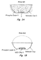
- a first approach is a slurry method involving the use of phosphor grains or particles 1 blended in a liquid polymer system, such as polypropylene, polycarbonate, epoxy resin, or silicone resin.
- a liquid polymer system such as polypropylene, polycarbonate, epoxy resin, or silicone resin.
- the mixed phosphor slurry is dispensed on or surrounding an LED chip 2, and then the liquid polymer system is dried or cured.
- the LED chip 2 along with the phosphor slurry can be disposed in a reflector cup 3, as depicted in Fig. 1A .
- a color temperature of a light emitting device can be determined by comparing its hue with a theoretical, heated blackbody radiator.
- a temperature, expressed in terms of degrees Kelvin, at which the heated blackbody radiator matches the hue of the light emitting device is that device's color temperature.
- An incandescent light source can be close to being a blackbody radiator, but many other light emitting devices do not emit radiation in the form of a blackbody curve and are, therefore, assigned a CCT.
- a CCT of a light emitting device is a color temperature of a blackbody radiator that most closely matches the device's perceived color. The higher the Kelvin rating, the "cooler" or more blue the light.
- a blue LED chip dispensed with a yellow phosphor by the slurry method can have a typical CCT that varies from about 5,800 K to about 7,200 K across a range of 1,400 K for light emission angles at ⁇ 70° from a center light-emitting axis of the LED. Because of the presence of colored rings, the CCT is typically higher at or near the center axis than in the periphery, where the emitted light tends to be more yellow.
- a second phosphor coating method is an Electrophoretic Deposition ("EPD") method for the manufacture of phosphor-converted white LEDs, as depicted in Fig. 1B .
- EPD Electrophoretic Deposition
- a phosphor is electrically charged by adding a proper amount of an electrolyte in a liquid solvent to form a liquid suspension, and is biased by an electrical field. Then, surface charged phosphor particles are moved to an electrode of counter-polarity and coated on the electrode. EPD of the phosphor particles creates a phosphor layer 4 of relatively uniform thickness that can produce white light of greater uniformity and reduced instances of colored rings. While achieving greater color uniformity, the EPD method is generally lacking in its ability to deposit phosphors directly over an electrically nonconductive surface.
- a phosphor layer is typically coated directly over a LED chip 5, according to the so-called proximate phosphor configuration.
- This configuration tends to be inefficient in terms of light scattering, since the proximate phosphor layer can direct about 60% of total white light emission back towards the LED chip 5, where high loss can occur.
- Another drawback of the EPD method is that certain phosphors are susceptible to degradation by the solvent, thereby limiting the general applicability of the EPD method.
- a luminescent ceramic plate 6 by heating phosphor particles at high pressure until surfaces of the phosphor particles begin to soften and melt. The partially melted particles can stick together to form the ceramic plate 6 including a rigid agglomerate of the particles.
- the luminescent ceramic plate 6 is disposed in a path of light emitted by an LED chip 7, which is disposed over a set of electrodes 8. While providing benefits in terms of robustness, reduced sensitivity to temperature, and reduced color variations from chip to chip, a resulting package efficiency can be unsatisfactory due to the proximate phosphor configuration.
- a scattering efficiency (also sometimes referred to as a package efficiency) is typically between 40% to 60% for commercially available white LEDs, with efficiency losses due to light absorption by internal package components such as an LED chip, a lead frame, or sub-mount.
- Fig. 3 depicts an example of a phosphor-converted white LED with yellow phosphor 31 powered by a blue LED chip 32, where a primary blue light 34 undergoing color mixing with a secondary light 35 of yellow color to generate a white color.
- a main source of light loss results from absorption of light by the LED chip 32. Because the LED chip 32 is typically formed of high-refractive index materials, photons tend to be trapped within the LED chip 32 due to Total Internal Reflection (“TIR”) once the photons strike and enter the LED chip 32.
- TIR Total Internal Reflection
- Another potential source of light loss results from imperfections in a mirror reflector 33 in the LED package.
- a primary light 36 emitted by the LED chip 32 can be reflected back to the chip 32 by the phosphor powders 31 or by the mirror reflector 33.
- Second, down-converted secondary light 37 emitted by the phosphor powders 31 can scatter backward towards the LED chip 32.
- Third, both primary light and secondary light 38 can be reflected back towards the chip 32 due to TIR at an air-LED package interface.
- a hemispheric lens 39 can be used to reduce instances of TIR at the air-package interface.
- the phosphor powders 31 desirably should not be placed directly over the chip surface, but rather should be placed at a certain distance from the LED chip 32. Furthermore, a thinner phosphor layer would reduce instances of backward scattering of secondary light by the phosphor powders 31.
- Certain embodiments of the invention relate to the formation of a thin-film phosphor layer of substantially uniform thickness that can be conformally disposed in an optical path of an LED, thereby producing substantially uniform white light with little or no colored rings.
- This thin-film phosphor layer can be prepared by an improved deposition method involving: (1) forming a phosphor powder layer that is substantially uniformly deposited on a substrate surface; and (2) forming a polymer binder layer to fill gaps among loosely packed phosphor particles, thereby forming a substantially continuous, thin-film phosphor layer.
- Phosphor conversion efficiency of the thin-film phosphor layer can be significantly improved because a thinner layer of a precisely controlled quantity of phosphor powders can be disposed in an optical path, thereby reducing light scattering losses.
- color homogeneity of the thin-film phosphor layer can be significantly improved due to substantially uniform deposition of phosphor particles.
- One method of forming an uniform, thin-film phosphor layer is to introduce electrostatic charges among phosphor particles during deposition of the phosphor particles. The electrostatic charges among the phosphor particles can self-balance and adjust their distribution, thereby promoting a substantially uniform distribution of the phosphor particles.
- Another method of forming an uniform, thin-film phosphor layer is through a phosphor dispensing mechanism, such as a showerhead mechanism in a deposition chamber, or through a rotational substrate holding mechanism, such as a turn table that holds a substrate.
- temperature stability of the thin-film phosphor layer can be significantly improved because the polymer binder layer can be thermally stable up to at least about 300°C or more.
- white color consistency can be maintained in a tight color coordinate by a coating process with precisely controlled quantities of deposited phosphor particles through a phosphor powder delivery mechanism.
- White color rendering can be precisely tuned with a layer-by-layer sequential deposition of multi-color phosphors, such as deposition of a red phosphor layer, deposition of a green phosphor layer, and then deposition of a blue phosphor layer.
- the ratio of multi-color phosphors can be precisely controlled in a resulting composite multi-color phosphor film stack.
- the color coordinate and CCT of a white LED fabricated by the phosphor thin-film process can be precisely controlled. This, in turn, can significantly simplify (or even avoid) a binning process.
- a consistent white color coordinate can be achieved from lightly varied blue LED chips by tuning the dosage of a multi-color phosphor film stack.
- This color compensation method can compensate for color variations of the blue LED chips using different compositions or amounts of phosphor contents. In such manner, white LED yield can be significantly increased for color sensitive applications, such as display backlighting using white LEDs.
- a thin-film phosphor coating method is a batch phosphor coating process. Multiple LED chips can be deposited with thin-film phosphor in one coating operation. According to another embodiment of the invention, multiple LED lenses can be deposited with thin-film phosphor in one coating operation. Similar to semiconductor chip manufacturing, a manufacturing cost per LED chip can be significantly reduced, and a manufacturing throughput can be significantly increased by a batch process.
- deposition of a thin-film phosphor layer can be used to form conformal thin-film phosphor layers directly over an electrically nonconductive surface.
- the conformal thin-film phosphor also can be deposited on a non-flat surface, such as a convex or concave surface of an LED lens.
- Some embodiments of the invention relate to a system for depositing a conformal thin-film phosphor layer on a substrate.
- the system can include a deposition chamber, a phosphor powder delivery subsystem, and a polymer precursor delivery subsystem configured to deliver a gas phase monomer to the deposition chamber.
- the system also can include a memory and a processor in electrical communication with the deposition chamber, the phosphor powder delivery subsystem, and the polymer precursor delivery subsystem, wherein the memory can include code or instructions stored therein and executable by the processor to form a thin-film phosphor layer.
- One specific embodiment of the invention relates to a method of forming a thin-film phosphor layer for use in a light emitting device.
- the method includes: (1) transporting, using a carrier gas, a phosphor powder from a source of the phosphor powder to a deposition chamber; and (2) depositing the phosphor powder adjacent to a substrate within the deposition chamber so as to substantially uniformly distribute the phosphor powder adjacent to a surface of the substrate.
- Another specific embodiment of the invention also relates to a method of forming a thin-film phosphor layer for use in a light emitting device.
- the method includes: (1) forming a first phosphor powder layer adjacent to a substrate, the first phosphor powder layer including first phosphor particles that are distributed adjacent to a surface of the substrate; and (2) forming, via vapor deposition, a first polymer layer adjacent to the first phosphor powder layer, the first polymer layer serving as a binder for the first phosphor particles.
- the system includes: (1) a deposition subsystem defining an enclosure to accommodate the substrate; (2) a phosphor powder delivery subsystem configured to deliver, using a carrier gas, a phosphor powder from a source of the phosphor powder to the deposition subsystem; (3) a polymer precursor delivery subsystem configured to deliver polymer precursors in a vapor phase to the deposition subsystem; and (4) a control subsystem connected to the deposition subsystem, the phosphor powder delivery subsystem, and the polymer precursor delivery subsystem, wherein the control subsystem is configured to control the phosphor powder delivery subsystem to deliver the phosphor powder to the deposition subsystem for a first time interval to form a phosphor powder layer adjacent to the substrate, and the control subsystem is configured to control the polymer precursor delivery subsystem to deliver the polymer precursors to the deposition subsystem for a second time interval to form a polymer layer adjacent to the phosphor powder layer
- a light emitting device which includes: (1) a substrate; (2) a phosphor powder layer substantially uniformly distributed adjacent to the substrate; and (3) a parylene-based polymer layer conformally deposited adjacent to the phosphor powder layer as a binder material to form a substantially continuous thin film, wherein the phosphor powder layer includes a single-color phosphor.
- a further specific embodiment of the invention relates to a light emitting device, which includes: (1) a substrate; (2) multiple phosphor powder layers substantially uniformly distributed adjacent to the substrate, the phosphor powder layers being configured to emit light of different colors; and (3) multiple parylene-based polymer layers, each of the parylene-based polymer layers being conformally deposited adjacent to a respective one of the phosphor powder layers, each of the parylene-based polymer layers being a binder material for a respective one of the phosphor powder layers to fill voids among constituent phosphor particles.
- a set refers to a collection of one or more components.
- a set of layers can include a single layer or multiple layers.
- Components of a set also can be referred to as members of the set.
- Components of a set can be the same or different.
- components of a set can share one or more common characteristics.
- adjacent refers to being near or adjoining. Adjacent components can be spaced apart from one another or can be in actual or direct contact with one another. In some instances, adjacent components can be connected to one another or can be formed integrally with one another.
- connection refers to an operational coupling or linking.
- Connected components can be directly coupled to one another or can be indirectly coupled to one another, such as via another set of components.
- the terms “substantially” and “substantial” refer to a considerable degree or extent. When used in conjunction with an event or circumstance, the terms can refer to instances in which the event or circumstance occurs precisely as well as instances in which the event or circumstance occurs to a close approximation, such as accounting for typical tolerance levels of the manufacturing operations described herein.
- electrically conductive and “electrical conductivity” refer to an ability to transport an electric current
- electrically nonconductive and “electrical nonconductivity” refer to a lack of ability to transport an electric current
- Electrically conductive materials typically correspond to those materials that exhibit little or no opposition to flow of an electric current
- electrically nonconductive materials typically correspond to those materials within which an electric current has little or no tendency to flow.
- One measure of electrical conductivity (or electrical nonconductivity) is in terms of Siemens per meter (“S ⁇ m -1 ").
- an electrically conductive material is one having a conductivity greater than about 10 4 S ⁇ m -1 , such as at least about 10 5 S ⁇ m -1 or at least about 10 6 S ⁇ m -1
- an electrically nonconductive material is one having a conductivity less than about 10 4 S ⁇ m -1 , such as less than or equal to about 10 3 S ⁇ m -1 or less than or equal to about 10 2 S ⁇ m -1
- Electrical conductivity (or electrical nonconductivity) of a material can sometimes vary with temperature. Unless otherwise specified, electrical conductivity (or electrical nonconductivity) of a material is defined at room temperature.
- Quantum efficiency refers to a ratio of the number of output photons to the number of input photons.
- a size of the particle can refer to a diameter of the particle.
- a size of the particle can refer to an average of various orthogonal dimensions of the particle.
- a size of a particle that is a spheroidal can refer to an average of a major axis and a minor axis of the particle.
- a size of a set of particles can refer to a typical size of a distribution of sizes, such as an average size, a median size, or a peak size.
- alkane refers to a saturated hydrocarbon molecule.
- an alkane can include from 1 to 100 carbon atoms.
- the term “lower alkane” refers to an alkane that includes from 1 to 20 carbon atoms, such as, for example, from 1 to 10 carbon atoms, while the term “upper alkane” refers to an alkane that includes more than 20 carbon atoms, such as, for example, from 21 to 100 carbon atoms.
- branched alkane refers to an alkane that includes one or more branches, while the term “unbranched alkane” refers to an alkane that is straight-chained.
- cycloalkane refers to an alkane that includes one or more ring structures.
- heteroalkane refers to an alkane that has one or more of its carbon atoms replaced by one or more heteroatoms, such as, for example, N, Si, S, O, and P.
- substituted alkane refers to an alkane that has one or more of its hydrogen atoms replaced by one or more substituent groups, such as, for example, halo groups, hydroxy groups, alkoxy groups, carboxy groups, thio groups, alkylthio groups, cyano groups, nitro groups, amino groups, alkylamino groups, dialkylamino groups, silyl groups, and siloxy groups, while the term “un-substituted alkane” refers to an alkane that lacks such substituent groups. Combinations of the above terms can be used to refer to an alkane having a combination of characteristics.
- branched lower alkane can be used to refer to an alkane that includes from 1 to 20 carbon atoms and one or more branches.
- alkanes include methane, ethane, propane, cyclopropane, butane, 2-methylpropane, cyclobutane, and charged, hetero, or substituted forms thereof.
- alkyl group refers to a monovalent form of an alkane.
- an alkyl group can be envisioned as an alkane with one of its hydrogen atoms removed to allow bonding to another group of a molecule.
- the term “lower alkyl group” refers to a monovalent form of a lower alkane, while the term “upper alkyl group” refers to a monovalent form of an upper alkane.
- the term “branched alkyl group” refers to a monovalent form of a branched alkane, while the term “unbranched alkyl group” refers to a monovalent form of an unbranched alkane.
- cycloalkyl group refers to a monovalent form of a cycloalkane
- heteroalkyl group refers to a monovalent form of a heteroalkane
- substituted alkyl group refers to a monovalent form of a substituted alkane
- un-substituted alkyl group refers to a monovalent form of an unsubstituted alkane
- alkyl groups include methyl, ethyl, n-propyl, isopropyl, cyclopropyl, butyl, isobutyl, t -butyl, cyclobutyl, and charged, hetero, or substituted forms thereof.
- an arene refers to an aromatic hydrocarbon molecule.
- an arene can include from 5 to 100 carbon atoms.
- the term “lower arene” refers to an arene that includes from 5 to 20 carbon atoms, such as, for example, from 5 to 14 carbon atoms, while the term “upper arene” refers to an arene that includes more than 20 carbon atoms, such as, for example, from 21 to 100 carbon atoms.
- the term “monocyclic arene” refers to an arene that includes a single aromatic ring structure, while the term “polycyclic arene” refers to an arene that includes more than one aromatic ring structure, such as, for example, two or more aromatic ring structures that are bonded via a carbon-carbon single bond or that are fused together.
- the term “heteroarene” refers to an arene that has one or more of its carbon atoms replaced by one or more heteroatoms, such as, for example, N, Si, S, O, and P.
- substituted arene refers to an arene that has one or more of its hydrogen atoms replaced by one or more substituent groups, such as, for example, alkyl groups, alkenyl groups, alkynyl groups, iminyl groups, halo groups, hydroxy groups, alkoxy groups, carboxy groups, thio groups, alkylthio groups, cyano groups, nitro groups, amino groups, alkylamino groups, dialkylamino groups, silyl groups, and siloxy groups, while the term “un-substituted arene” refers to an arene that lacks such substituent groups. Combinations of the above terms can be used to refer to an arene having a combination of characteristics.
- the term "monocyclic lower alkene” can be used to refer to an arene that includes from 5 to 20 carbon atoms and a single aromatic ring structure.
- examples of arenes include benzene, biphenyl, naphthalene, pyridine, pyridazine, pyrimidine, pyrazine, quinoline, isoquinoline, and charged, hetero, or substituted forms thereof.
- aryl group refers to a monovalent form of an arene.
- an aryl group can be envisioned as an arene with one of its hydrogen atoms removed to allow bonding to another group of a molecule.
- lower aryl group refers to a monovalent form of a lower arene
- upper aryl group refers to a monovalent form of an upper arene.
- monocyclic aryl group refers to a monovalent form of a monocyclic arene
- polycyclic aryl group refers to a monovalent form of a polycyclic arene.
- heteroaryl group refers to a monovalent form of a heteroarene.
- substituted aryl group refers to a monovalent form of a substituted arene
- un-substituted arene group refers to a monovalent form of an unsubstituted arene.
- aryl groups include phenyl, biphenylyl, naphthyl, pyridinyl, pyridazinyl, pyrimidinyl, pyrazinyl, quinolyl, isoquinolyl, and charged, hetero, or substituted forms thereof.
- arylene group refers to a bivalent form of an arene.
- an arylene group can be envisioned as an arene with two of its hydrogen atoms removed to allow bonding to one or more additional groups of a molecule.
- the term “lower arylene group” refers to a bivalent form of a lower arene, while the term “upper arylene group” refers to a bivalent form of an upper arene.
- monocyclic arylene group refers to a bivalent form of a monocyclic arene, while the term “polycyclic arylene group” refers to a bivalent form of a polycyclic arene.
- heteroarylene group refers to a bivalent form of a heteroarene.
- substituted arylene group refers to a bivalent form of a substituted arene, while the term “un-substituted arylene group” refers to a bivalent form of an unsubstituted arene.
- arylene groups include phenylene, biphenylylene, naphthylene, pyridinylene, pyridazinylene, pyrimidinylene, pyrazinylene, quinolylene, isoquinolylene, and charged, hetero, or substituted forms thereof.
- a thin-film conformal phosphor deposition process for phosphor-converted white LEDs. This process facilitates achieving the goal of increasing light scattering efficiency for white LEDs by providing a thin-film and remote phosphor layer configuration.
- a thin-film phosphor layer can be substantially uniformly and conformally deposited on a flat or non-flat and electrically conductive, semiconductive, or nonconductive surface by two operations: (1) forming a phosphor powder layer that is substantially uniformly deposited on the substrate surface (operation 42); and (2) forming a polymer binder layer to fill gaps among phosphor particles to form a substantially continuous layer of thin film (operation 44).
- the deposition process of forming the thin-film phosphor layer is desirably held in a vacuum chamber. However, it will be appreciated that the deposition process also can take place in a deposition chamber filled with an inert gas, such as nitrogen, or in an atmospheric environment.
- an inert gas such as nitrogen
- a variety of phosphors can be used.
- a phosphor is formed from a luminescent material, namely one that emits light in response to an energy excitation.
- Luminescence can occur based on relaxation from excited electronic states of atoms or molecules and, in general, can include, for example, chemiluminescence, electroluminescence, photoluminescence, thermoluminescence, triboluminescence, and combinations thereof.
- photoluminescence which can include fluorescence and phosphorescence
- an excited electronic state can be produced based on a light excitation, such as absorption of light.
- inorganic host materials doped by activator ions such as Ce 3+ and Eu 2+ , including garnets (e.g., (Y 1-a Gd a ) 3 (Al 1-b Ga b ) 5 O 12 :Ce 3+ with a, b ⁇ 0.2 or YAG:Ce 34 ), silicates, orthosilicates, sulfides, and nitrides.
- Garnets and orthosilicates can be used as yellow-emitting phosphors, and nitrides can be used as red-emitting phosphors.
- various other types of wavelength-conversion materials can be used, including organic dyes.
- phosphors and other types of wavelength-conversion materials can exhibit photoluminescence with a quantum efficiency that is greater than about 30 percent, such as at least about 40 percent, at least about 50 percent, at least about 60 percent, at least about 70 percent, or at least about 80 percent, and can be up to about 90 percent or more.
- a phosphor used in accordance with Fig. 4 is provided in a powder form, namely as a set of particles.
- the particles desirably have sizes in the range of about 1 nm to about 100 ⁇ m, such as from about 10 nm to about 30 ⁇ m, from about 100 nm to about 30 ⁇ m, from about 500 nm to about 30 ⁇ m, or from about 1 ⁇ m to about 30 ⁇ m.
- the phosphor powder can be transported and deposited over the substrate surface by inertia effects, Brownian movement, thermophoresis, or electrical fields if the phosphor powder is electrically charged.
- One approach to form a substantially uniformly distributed phosphor powder layer on the substrate surface is to entrain, carry, mobilize, or transport the phosphor powder from a phosphor canister by a set of carrier gases, such as clean, dry air or an inert gas such as nitrogen, and then spray the phosphor powder through a showerhead mechanism in a vacuum, inert gas, or atmospheric chamber.
- the phosphor powder is ionized with the same positive or negative electrostatic charge during the phosphor transport process.
- electrostatic spraying of the phosphor powder involves:
- the phosphor powder is ionized with electrostatic charges by one, or a combination, of the following methods:
- the substrate surface can be grounded to maintain an electric field potential for the deposition of the electrostatically charged phosphor powder.
- Electrostatic charges also can be created on the phosphor powder or an electrically nonconductive substrate surface by Tribo frictional charging.
- Tribo frictional charging when two different materials are brought into contact, there can be a transfer of charge from one to the other to offset an imbalance of charges. The magnitude and direction of the charge transfer can depend on a number of factors, including a chemical and electronic structure of both materials. Table 1 sets forth certain materials ranging from those with the most positive charging effect to those with the most negative charging effect when brought into contact.
- Table 1 Materials ordered by Triboelectric Charging Effects Most Positive (+) Air Human Hands, Skin Asbestos Rabbit Fur +++ Glass Human Hair Mica Nylon Wool Lead Cat Fur + Silk Aluminum Paper Cotton Steel Wood Lucite Sealing Wax Amber Rubber Balloon Hard Rubber Mylar Nickel Copper Silver UV Resist Brass Synthetic Rubber Gold, Platinum Sulfur Acetate, Rayon Polyester - - - Celluloid Polystyrene Orlon, Acrylic Cellophane Tape Polyvinylidene chloride (Saran) Polyurethane Polyethylene Polypropylene Polyvinylchloride (Vinyl) Kel-F (PCTFE) Silicon Teflon Silicone Rubber Most Negative (-)
- An opposite electrostatic charge can be created on an electrically nonconductive substrate surface with the Tribo frictional charging method.
- negative charges can be created on the nonconductive substrate surface by one, or a combination, of the following:
- the phosphor deposition process provides a number of advantages, including:
- the deposited phosphor layer is initially a loosely packed powder layer.
- a polymer thin film is deposited to fill gaps among phosphor particles and to form a substantially continuous thin-film layer, as depicted in operation 44 of Fig. 4 .
- CVD Chemical Vapor Deposition
- another suitable deposition process can be used in place of, or in conjunction with, CVD to form the polymer layer.
- deposition processes include other vapor deposition processes, such as thermal evaporation, electron-beam evaporation, or physical vapor deposition, as well as spray coating, dip coating, web coating, wet coating, and spin coating.
- Fig. 6A through Fig. 6D depict examples of a family of conformal coating polymers that can be used to form a binding matrix for a thin-film phosphor layer, according to an embodiment of the invention.
- the family of polymers corresponds to a family of parylene-based polymers.
- parylene-based polymers correspond to a variety of polyxylylene-based polymers, such as poly( p -xylylene) and its derivatives, and include, for example, polymers having a general repeating unit of the formula -CZZ'-Ar-CZ"Z"'-, wherein Ar is an arylene group (e.g., un-substituted, partially substituted, or fully substituted arylene group, such as phenylene), and wherein Z, Z', Z", and Z'" can be the same or different.
- Ar is an arylene group (e.g., un-substituted, partially substituted, or fully substituted arylene group, such as phenylene)
- Z, Z', Z", and Z'" can be the same or different.
- Parylene N depicted in Fig. 6A includes a repeating unit of the formula -CH 2 -C 6 H 4 -CH 2 -, and is used as a binder material to form a thin-film phosphor layer.
- Parylene C can be produced from the same monomer as Parylene N, but modified with the substitution of a chlorine atom for one of the aromatic hydrogens.
- Parylene D depicted in Fig. 6C including a repeating unit of the formula -CH 2 -C 6 H 2 Cl 2 -CH 2 - is used as a binder material to form a thin-film phosphor layer. Parylene D can be produced from the same monomer as Parylene N, but modified with the substitution of two chlorine atoms for two of the aromatic hydrogens.
- Parylene F a partially fluorinated parylene-based polymer referred to as Parylene F can be used, as depicted in Fig. 6D .
- Parylene F includes a repeating unit of the formula -CF 2 -C 6 H 4 -CF 2 -, and can be formed from various precursors, such as BrCF 2 -C 6 H 4 -CF 2 Br. It will be appreciated that these parylene-based polymers are provided by way of example, and a variety of other conformal coating polymers can be used.
- polyimides examples include polyimides, fluorocarbon-based polymers (e.g., poly(tetrafluoroethylene)), poly(p-phenylene vinylene), poly(pyrrole), poly(thiophene), poly(2,4-hexadiyn-1,6-diol), fluorocarbon/organosilicon copolymers, poly(ethylene glycol), and their derivatives.
- fluorocarbon-based polymers e.g., poly(tetrafluoroethylene)
- poly(p-phenylene vinylene) poly(pyrrole)
- poly(thiophene) poly(2,4-hexadiyn-1,6-diol)
- fluorocarbon/organosilicon copolymers examples include poly(ethylene glycol), and their derivatives.
- Thermal evaporation of acrylics also can be used to form a substantially continuous phosphor film.
- Transport polymerization typically involves generating a vapor phase reactive intermediate from a precursor molecule at a location remote from a substrate surface, and then transporting the vapor phase reactive intermediate to the substrate surface.
- the substrate surface can be kept below a melting temperature of reactive intermediates for polymerization.
- Parylene F can be formed from the precursor BrCF 2 -C 6 H 4 -CF 2 Br by the removal of the bromine atoms to form the reactive intermediate *CF 2 -C 6 H 4 -CF 2 *, wherein * denotes a free radical.
- This reactive intermediate can be formed at a location remote from a deposition chamber, and can be transported into the deposition chamber and condensed over the substrate surface, where polymerization takes place.
- parylene-based polymer films can be formed from a variety of precursors, such as those having the formula (CZZ'Y) m -Ar-(CZ"Z"'Y') n , wherein Ar is an arylene group (e.g., un-substituted, partially substituted, or fully substituted arylene group, such as phenylene), Z, Z', Z", and Z'" can be the same or different, Y and Y' can be the same or different and are removable to generate free radicals, m and n are each equal to zero or a positive integer, and a sum of m and n is less than or equal to a total number of sp 2 -hybridized carbons on Ar available for substitution.
- precursors such as those having the formula (CZZ'Y) m -Ar-(CZ"Z"'Y') n , wherein Ar is an arylene group (e.g., un-substituted, partially substitute
- X is a halogen such as Cl or F
- x 0, 1, 2, 3, or 4
- Ar is an arylene group (e.g., un-substituted, partially substituted, or fully substituted arylene group, such as phenylene)
- Z, Z', Z", and Z'" can be the same or different.
- X is a halogen such as Cl or F
- x 0, 1, 2, 3, or 4
- parylene-based polymer film, or another type of polymer film, prepared by the CVD method is that it is a conformal coating with superior crevice penetration capability, thereby substantially filling gaps and voids within a phosphor powder layer.
- Parylene F can achieve the best result for gap-filling
- Parylene N can achieve the second best result for gap-filling among the family of parylene-based polymers.
- Another aspect of a parylene-based polymer is that it has superior optical transparency in the visible light spectrum, rendering it a suitable filler material among a photoluminescent phosphor powder.
- Another aspect of a parylene-based polymer is that its refractive index can be adjusted based on chemical composition.
- a multi-layer of parylene-based polymer films can be formed as a composite thin-film phosphor stack.
- This multi-layer structure can be formed by depositing a Parylene N film, with a refractive index of about 1.66, as a binder material among a phosphor powder, and then depositing a Parylene F film, with a refractive index of about 1.4, thereby enhancing light extraction due to index matching of the Parylene F film to ambient environment (e.g., air).
- this multi-layer structure can be formed by depositing a first polymer film, with a first refractive index, as a binder material among a first phosphor powder layer to form a first phosphor layer adjacent to the substrate surface, depositing a second polymer film, with a second refractive index, as a binder material among a second phosphor powder layer to form a second phosphor layer adjacent to the first phosphor layer, and so on, where the first refractive index is greater than or equal to the second refractive index.
- a parylene-based polymer, or another type of polymer can be formed as a substantially continuous film having a thickness in the range of a few tens of angstroms to about 100 ⁇ m, such as from about 1 nm to about 100 ⁇ m, from about 10 nm to about 100 ⁇ m, from about 100 nm to about 100 ⁇ m, from about 1 ⁇ m to about 100 ⁇ m, from about 1 ⁇ m to about 75 ⁇ m, from about 1 ⁇ m to about 30 ⁇ m, or from about 1 ⁇ m to about 10 ⁇ m.
- the thickness of the film can exhibit a standard deviation of less than about 20 percent with respect to an average thickness, such as less than about 10 percent or less than about 5 percent.
- a thickness of the initially deposited phosphor powder layer can be in the range of about 1 nm to about 60 ⁇ m, such as from about 10 nm to about 60 ⁇ m, from about 100 nm to about 40 ⁇ m, or from about 100 nm to about 20 ⁇ m.
- the thickness of the phosphor powder layer can exhibit a standard deviation of less than about 20 percent with respect to an average thickness, such as less than about 10 percent or less than about 5 percent.
- a distribution of the phosphor powder within the resulting film can be substantially uniform across an extent of the film, such that a weight density (e.g., mass or weight of phosphor particles per unit volume) or a number density (e.g., number of phosphor particles per unit volume) can exhibit a standard deviation of less than about 20 percent with respect to an average density, such as less than about 10 percent or less than about 5 percent.
- a weight density e.g., mass or weight of phosphor particles per unit volume
- a number density e.g., number of phosphor particles per unit volume
- a thin-film phosphor layer prepared by the CVD method is depicted in Fig. 7A .
- a single-color phosphor powder layer 71 such as a YAG:Ce 3+ -based yellow phosphor, is initially deposited on a substrate surface 72.
- the substrate surface 72 can be an electrically nonconductive surface, such as a surface of a flexible plastic substrate.
- a parylene-based polymer layer 73 is deposited, and another parylene-based polymer layer 74 is next deposited.
- the parylene-based polymer layer 73 serves as a binder or a matrix that at least partially penetrates or surrounds the phosphor powder layer 71, such that phosphor particles of the phosphor powder layer 71 are dispersed within the parylene-based polymer layer 73. It will be appreciated that the parylene-based polymer layers 73 and 74 can be formed from the same material or different materials. In some instances, a refractive index of the parylene-based polymer layer 73 is greater than a refractive index of the parylene-based polymer layer 74.
- a multi-color phosphor thin-film stack 75 is formed by sequential deposition of a blue phosphor powder, a parylene-based polymer as a binder material for the blue phosphor powder, a green phosphor powder, a parylene-based polymer as a binder material for the green phosphor powder, a red phosphor power, and a parylene-based polymer as a binder material for the red phosphor powder.
- a resulting phosphor-converted white LED can emit three down-converted secondary lights of respective colors by the phosphors.
- a Color Rendering Index (“CRI") of the phosphor-converted white LED can be readily tuned, for example, when used in an indoor general illumination application with a warmer white light and an improved color uniformity.
- Another application of the phosphor-converted white LED incorporating the multi-color thin-film phosphor stack 75 is for backlighting of Liquid Crystal Displays ("LCDs").
- the phosphor powder deposition in operation 42 and the polymer deposition in operation 44 need not take place sequentially. Alternatively, these operations can take place substantially simultaneously to form a conformal phosphor thin-film layer.
- Fig. 8 depicts a thin-film phosphor deposition system 80, according to an embodiment of the invention.
- the thin-film phosphor deposition system 80 can be used to form a conformally coated thin-film phosphor layer by depositing a substantially uniformly distributed phosphor powder layer and then depositing a conformally coated CVD polymer to form a substantially continuous phosphor thin film.
- the thin-film phosphor deposition system 80 includes: (1) a deposition subsystem or unit 81; (2) a phosphor powder delivery subsystem or unit 82 connected to the deposition subsystem 81; and (3) a parylene-based polymer precursor delivery subsystem or unit 83 connected to the deposition subsystem 81.
- the deposition subsystem 81 includes: (1) a deposition chamber 81a, which defines an enclosure within which a substrate is disposed and, for example, is a vacuum chamber with an associated vacuum pump to maintain vacuum conditions, is filled with an inert gas, or is an atmospheric chamber; (2) a substrate holder 81b within the chamber 81a and, for example, is capable of rotating the substrate during the formation of the phosphor film; (3) a showerhead mechanism 81c; and (4) a phosphor powder ionizer 81d, which introduces electrostatic charges among phosphor particles during phosphor powder deposition.
- the phosphor powder delivery subsystem 82 includes: (1) a phosphor powder canister 82a or other phosphor powder source; (2) a phosphor flow controller 82b, which regulates a specified quantity of phosphors for each deposition of phosphors; (3) an ionizer 82c, which introduces electrostatic charges among phosphor particles during phosphor powder deposition; and (4) a set of valves 82d.
- the parylene-based polymer precursor delivery subsystem 83 includes: (1) a precursor canister 83a or other precursor source; (2) a precursor flow controller 83b, which regulates a specified quantity of precursors for each polymer deposition; (3) a gas reactor 83c, which induces the generation of vapor phase reactive intermediates from precursors; and (4) a set of valves 83d.
- solid or liquid precursors are heated in the stainless canister 83a to a consistent temperature to generate vapor phase precursors.
- the vapor phase precursors are fed into the gas reactor 83c, which is regulated by the flow controller 83b, as depicted in Fig. 8 .
- the gas reactor 83c splits the precursors into reactive intermediates that bear two unpaired electrons, or diradicals.
- the diradicals are transported to the deposition chamber 81a shortly after the gas reactor 83c activates the precursors. Because the diradicals can be very reactive, the diradicals can quickly polymerize to form a polymer thin film once the diradicals collide with each other on a substrate surface held inside the deposition chamber 81a.
- the thin-film phosphor deposition system 80 also includes a control subsystem or unit, which includes a processor 84 and an associated memory 85 that are connected to other components of the system 80 and serve to direct operation of those components.
- the memory 85 can include a computer-readable storage medium having computer code stored thereon for performing various computer-implemented operations.
- the media and computer code can be those specially designed and constructed for the purposes of embodiments of the invention, or they may be of the kind well known and available to those having skill in the computer software arts.
- Examples of computer-readable media include, but are not limited to: magnetic storage media such as hard disks, floppy disks, and magnetic tape; optical storage media such as Compact Disc/Digital Video Discs ("CD/DVDs”), Compact Disc-Read Only Memories (“CD-ROMs”), and holographic devices; magneto-optical storage media such as floptical disks; and hardware devices that are specially configured to store and execute program code, such as Application-Specific Integrated Circuits ("ASICs”), Programmable Logic Devices (“PLDs”), and ROM and RAM devices.
- Examples of computer code include, but are not limited to, machine code, such as produced by a compiler, and files containing higher-level code that are executed by a computer using an interpreter.
- an embodiment of the invention may be implemented using Java, C++, or other object-oriented programming language and development tools.
- Additional examples of computer code include, but are not limited to, encrypted code and compressed code.
- Other embodiments of the invention can be implemented using hardwired circuitry in place of, or in conjunction with, computer code.
- Table 2 sets forth certain advantages of the conformal thin-film phosphor deposition method of some embodiments of the invention, relative to other phosphor coating methods.
- Table 2 Comparison of Phosphor Coating Methods Slurry Method EPD Ceramic Plate Conformal Thin-Film Phosphor Spatial Phosphor Distribution proximate phosphor-in-cup proximate conformal phosphor proximate phosphor remote conformal phosphor Scattering Efficiency ⁇ 50% ⁇ 40% Slightly better than EPD ⁇ about 90% (e.g., ⁇ about 92% or ⁇ about 95% and up to about 99% or more) Homogeneity Poor Good Good Good Color Consistency Poor Good Good Good Color Rendering Possible for multi-color phosphor Single phosphor Possible for multi-layer ceramic plate Possible for layer-by-layer phosphor deposition Temperature Stability Medium Poor Good Best Cost Die-level process Batch process Die-level process Batch process Die-level process Batch process
- a light emitting device formed in accordance with the conformal thin-film phosphor deposition method can emit white light of greater uniformity.
- a CCT variation of a white light LED can be no greater than about 1,000 K over a 140° ( ⁇ 70° from a center light-emitting axis) range of light emission angles, such as no greater than about 800 K, no greater than about 500 K, or no greater than about 300 K, and down to about 200 K or less.
Landscapes
- Chemical & Material Sciences (AREA)
- Engineering & Computer Science (AREA)
- Materials Engineering (AREA)
- Organic Chemistry (AREA)
- General Chemical & Material Sciences (AREA)
- Chemical Kinetics & Catalysis (AREA)
- Mechanical Engineering (AREA)
- Metallurgy (AREA)
- Inorganic Chemistry (AREA)
- Led Device Packages (AREA)
- Laminated Bodies (AREA)
- Polyoxymethylene Polymers And Polymers With Carbon-To-Carbon Bonds (AREA)
- Luminescent Compositions (AREA)
Applications Claiming Priority (3)
| Application Number | Priority Date | Filing Date | Title |
|---|---|---|---|
| US11419808P | 2008-11-13 | 2008-11-13 | |
| PCT/US2009/064434 WO2010057023A2 (fr) | 2008-11-13 | 2009-11-13 | Système et procédé pour former une couche mince de phosphore pour dispositifs électroluminescents à conversion au phosphore |
| EP09826855.0A EP2412037B1 (fr) | 2008-11-13 | 2009-11-13 | Système et procédé pour former une couche mince de phosphore pour dispositifs électroluminescents à conversion au phosphore |
Related Parent Applications (2)
| Application Number | Title | Priority Date | Filing Date |
|---|---|---|---|
| EP09826855.0A Division EP2412037B1 (fr) | 2008-11-13 | 2009-11-13 | Système et procédé pour former une couche mince de phosphore pour dispositifs électroluminescents à conversion au phosphore |
| EP09826855.0A Division-Into EP2412037B1 (fr) | 2008-11-13 | 2009-11-13 | Système et procédé pour former une couche mince de phosphore pour dispositifs électroluminescents à conversion au phosphore |
Publications (2)
| Publication Number | Publication Date |
|---|---|
| EP2930758A1 true EP2930758A1 (fr) | 2015-10-14 |
| EP2930758B1 EP2930758B1 (fr) | 2019-05-22 |
Family
ID=42165459
Family Applications (2)
| Application Number | Title | Priority Date | Filing Date |
|---|---|---|---|
| EP09826855.0A Active EP2412037B1 (fr) | 2008-11-13 | 2009-11-13 | Système et procédé pour former une couche mince de phosphore pour dispositifs électroluminescents à conversion au phosphore |
| EP15167769.7A Active EP2930758B1 (fr) | 2008-11-13 | 2009-11-13 | Système de formation d'une couche mince de phosphore pour dispositifs électroluminescents à conversion au phosphore |
Family Applications Before (1)
| Application Number | Title | Priority Date | Filing Date |
|---|---|---|---|
| EP09826855.0A Active EP2412037B1 (fr) | 2008-11-13 | 2009-11-13 | Système et procédé pour former une couche mince de phosphore pour dispositifs électroluminescents à conversion au phosphore |
Country Status (7)
| Country | Link |
|---|---|
| US (2) | US20100119839A1 (fr) |
| EP (2) | EP2412037B1 (fr) |
| JP (2) | JP5723781B2 (fr) |
| KR (1) | KR101697798B1 (fr) |
| CN (2) | CN105655469B (fr) |
| TW (1) | TWI508331B (fr) |
| WO (1) | WO2010057023A2 (fr) |
Families Citing this family (48)
| Publication number | Priority date | Publication date | Assignee | Title |
|---|---|---|---|---|
| US8323998B2 (en) * | 2009-05-15 | 2012-12-04 | Achrolux Inc. | Methods and apparatus for forming uniform layers of phosphor material on an LED encapsulation structure |
| TWI564427B (zh) * | 2009-12-18 | 2017-01-01 | 財團法人工業技術研究院 | 聚對二甲苯薄膜的形成方法 |
| TWI452733B (zh) * | 2009-12-26 | 2014-09-11 | Achrolux Inc | 用於轉換發光波長之均勻膜層結構及其形成方法 |
| DE102010034923A1 (de) * | 2010-08-20 | 2012-02-23 | Osram Opto Semiconductors Gmbh | Verfahren zur Herstellung eines Schichtverbunds aus einer Lumineszenzkonversionsschicht und einer Streuschicht |
| US20120154917A1 (en) * | 2011-01-18 | 2012-06-21 | Eric William Hearn Teather | Color-shifting reflector |
| US8492182B2 (en) | 2011-04-29 | 2013-07-23 | Osram Opto Semiconductors Gmbh | Method for the producing of a light-emitting semiconductor chip, method for the production of a conversion die and light-emitting semiconductor chip |
| US8921875B2 (en) * | 2011-05-10 | 2014-12-30 | Cree, Inc. | Recipient luminophoric mediums having narrow spectrum luminescent materials and related semiconductor light emitting devices and methods |
| US8657200B2 (en) | 2011-06-20 | 2014-02-25 | Metrologic Instruments, Inc. | Indicia reading terminal with color frame processing |
| CN102856477B (zh) * | 2011-11-22 | 2015-09-09 | 深圳市光峰光电技术有限公司 | 一种荧光粉片层的制作方法及制作系统 |
| CN102492416A (zh) * | 2011-11-28 | 2012-06-13 | 斯迪克新型材料(江苏)有限公司 | 一种用于led灯的聚酯薄膜 |
| US8816371B2 (en) * | 2011-11-30 | 2014-08-26 | Micron Technology, Inc. | Coated color-converting particles and associated devices, systems, and methods |
| KR20130078764A (ko) * | 2011-12-30 | 2013-07-10 | 코오롱인더스트리 주식회사 | 투명 전도성 필름 |
| DE102012208900A1 (de) * | 2012-05-25 | 2013-11-28 | Osram Opto Semiconductors Gmbh | Verfahren zum Herstellen optoelektronischer Bauelemente und Vorrichtung zum Herstellen optoelektronischer Bauelemente |
| DE102012212086A1 (de) * | 2012-07-11 | 2014-01-16 | Osram Opto Semiconductors Gmbh | Verfahren zum herstellen einer komponente eines optoelektronischen bauelements und verfahren zum herstellen eines optoelektronischen bauelements |
| CN103633226B (zh) * | 2012-08-21 | 2016-12-21 | 广州市晶鑫光电科技有限公司 | 荧光粉胶体制备方法及相应的发光二极管封装方法 |
| DE102012109177A1 (de) * | 2012-09-27 | 2014-04-17 | Osram Opto Semiconductors Gmbh | Optoelektronisches Halbleiterbauelement |
| CN102983251B (zh) * | 2012-11-27 | 2016-02-03 | 北京半导体照明科技促进中心 | 极化荧光粉、荧光粉的极化方法及led发光器件的制作方法 |
| KR101462377B1 (ko) * | 2013-01-30 | 2014-11-17 | 주식회사 효성 | 파장변환용 광학시트의 제조방법 및 이로부터 제조된 광학시트 |
| TWI512385B (zh) | 2013-10-07 | 2015-12-11 | 中強光電股份有限公司 | 光波長轉換模組、照明系統以及投影裝置 |
| KR101584201B1 (ko) | 2014-01-13 | 2016-01-13 | 삼성전자주식회사 | 반도체 발광소자 및 이의 제조방법 |
| US20160186320A1 (en) * | 2014-12-26 | 2016-06-30 | Metal Industries Research And Development Centre | Apparatus for continuously forming a film through chemical vapor deposition |
| DE102015107586B4 (de) * | 2015-05-13 | 2023-10-26 | OSRAM Opto Semiconductors Gesellschaft mit beschränkter Haftung | Verfahren zur Herstellung optoelektronischer Bauelemente und oberflächenmontierbares optoelektronisches Bauelement |
| US10693046B2 (en) | 2015-12-30 | 2020-06-23 | Maven Optronics Co., Ltd. | Chip scale packaging light emitting device and manufacturing method of the same |
| TWI581465B (zh) * | 2015-12-30 | 2017-05-01 | 行家光電股份有限公司 | 晶片級封裝發光裝置及其製造方法 |
| CN106981554B (zh) * | 2016-01-19 | 2019-05-07 | 行家光电股份有限公司 | 具凹形设计的芯片级封装发光装置及其制造方法 |
| US10615320B2 (en) | 2016-01-12 | 2020-04-07 | Maven Optronics Co., Ltd. | Recessed chip scale packaging light emitting device and manufacturing method of the same |
| US10230030B2 (en) | 2016-01-28 | 2019-03-12 | Maven Optronics Co., Ltd. | Light emitting device with asymmetrical radiation pattern and manufacturing method of the same |
| US10797209B2 (en) | 2016-02-05 | 2020-10-06 | Maven Optronics Co., Ltd. | Light emitting device with beam shaping structure and manufacturing method of the same |
| US10620478B2 (en) | 2016-05-30 | 2020-04-14 | Maven Optronics Co., Ltd. | Photoluminescent display device and method for manufacturing the same |
| US10230027B2 (en) | 2016-08-05 | 2019-03-12 | Maven Optronics Co., Ltd. | Moisture-resistant chip scale packaging light-emitting device |
| CN107706281B (zh) * | 2016-08-09 | 2019-07-19 | 行家光电股份有限公司 | 具湿气阻隔结构的晶片级封装发光装置 |
| TWI599078B (zh) * | 2016-08-05 | 2017-09-11 | 行家光電股份有限公司 | 具濕氣阻隔結構之晶片級封裝發光裝置 |
| US10319789B2 (en) * | 2016-08-12 | 2019-06-11 | Osram Opto Semiconductors Gmbh | Method for producing an optoelectronic component and an optoelectronic component |
| CN106768838B (zh) * | 2016-12-08 | 2023-07-28 | 中铁十四局集团第二工程有限公司 | 一种复杂条件下浆-水相界面移动追踪观测装置及方法 |
| US10730276B2 (en) | 2017-01-17 | 2020-08-04 | Maven Optronics Co., Ltd. | System and method for vacuum film lamination |
| US10522728B2 (en) | 2017-01-26 | 2019-12-31 | Maven Optronics Co., Ltd. | Beveled chip reflector for chip-scale packaging light-emitting device and manufacturing method of the same |
| US11047747B2 (en) | 2017-03-27 | 2021-06-29 | Firouzeh Sabri | Light weight flexible temperature sensor kit |
| CN108803213B (zh) | 2017-04-27 | 2021-03-19 | 中强光电股份有限公司 | 波长转换滤光模块以及照明系统 |
| TWI627064B (zh) * | 2017-08-08 | 2018-06-21 | Southern Taiwan University Of Science And Technology | 複合板及其應用 |
| US10541353B2 (en) | 2017-11-10 | 2020-01-21 | Cree, Inc. | Light emitting devices including narrowband converters for outdoor lighting applications |
| CN108511566A (zh) * | 2018-03-13 | 2018-09-07 | 广东省半导体产业技术研究院 | 一种发光二极管制作方法 |
| WO2019239850A1 (fr) * | 2018-06-12 | 2019-12-19 | 日本電気硝子株式会社 | Module de conversion de longueur d'onde et élément de conversion de longueur d'onde, et procédé de fabrication associé, et dispositif electroluminescent |
| US12002665B2 (en) * | 2019-07-01 | 2024-06-04 | Applied Materials, Inc. | Real-time detection of particulate matter during deposition chamber manufacturing |
| GB2588932B (en) * | 2019-11-15 | 2022-08-24 | Dyson Technology Ltd | Method and apparatus for sputter deposition of target material to a substrate |
| CN111221210B (zh) * | 2020-01-16 | 2020-11-10 | 无锡视美乐激光显示科技有限公司 | 波长转换机构、投影装置及荧光激发方法 |
| KR102297774B1 (ko) * | 2021-02-09 | 2021-09-03 | (주)테라시스 | 분말 스프레이 방식을 이용한 기능성 시트 및 이의 제조 방법 |
| CN113686944B (zh) * | 2021-08-31 | 2024-03-12 | 江苏双星彩塑新材料股份有限公司 | 一种薄膜电晕处理表面的检测方法及系统 |
| CN115529708B (zh) * | 2022-09-29 | 2026-03-17 | 南京工业大学 | 一种生成荧光显色薄膜的等离子体改性装置及其控制方法 |
Citations (4)
| Publication number | Priority date | Publication date | Assignee | Title |
|---|---|---|---|---|
| EP1286364A2 (fr) * | 2001-08-23 | 2003-02-26 | Agfa-Gevaert N.V. | Panneau contenant un matériau luminescent à bonne résistance à l'humidité |
| US20060033040A1 (en) * | 2004-08-10 | 2006-02-16 | Canon Kabushiki Kaisha | Radiation detecting apparatus, manufacturing method thereof, scintillator panel and radiation detecting system |
| WO2007005013A1 (fr) * | 2005-07-01 | 2007-01-11 | Lamina Lighting, Inc. | Dispositifs d'éclairage comprenant des diodes et des réseaux à diodes électroluminescentes blanches, ainsi que procédé et appareil permettant de fabriquer ces dispositifs |
| US20080238294A1 (en) * | 2007-03-30 | 2008-10-02 | The Penn State Research Foundation | Mist fabrication of quantum dot devices |
Family Cites Families (52)
| Publication number | Priority date | Publication date | Assignee | Title |
|---|---|---|---|---|
| NL135549C (fr) * | 1966-04-22 | |||
| US5466947A (en) * | 1994-03-18 | 1995-11-14 | Bio-Rad Laboratories, Inc. | Protective overlayer for phosphor imaging screen |
| US5567468A (en) * | 1994-10-11 | 1996-10-22 | Schonbek Worldwide Lighting Inc. | Method and apparatus for applying powder coatings to surfaces |
| DE29724847U1 (de) * | 1996-06-26 | 2004-09-30 | Osram Opto Semiconductors Gmbh | Lichtabstrahlendes Halbleiterbauelement mit Lumineszenzkonversionselement |
| US5959316A (en) * | 1998-09-01 | 1999-09-28 | Hewlett-Packard Company | Multiple encapsulation of phosphor-LED devices |
| JP2000071451A (ja) * | 1998-09-02 | 2000-03-07 | Konica Corp | 圧電セラミック素子及びその製造方法 |
| JP4155986B2 (ja) * | 1998-10-20 | 2008-09-24 | 株式会社日本触媒 | 含ハロゲン芳香族化合物 |
| TWI222433B (en) * | 1998-10-20 | 2004-10-21 | Nippon Catalytic Chem Ind | Method for production of halogen-containing aromatic compound |
| JP4985507B2 (ja) * | 1999-07-21 | 2012-07-25 | 富士ゼロックス株式会社 | 画像形成装置、画像形成方法、及び画像表示媒体 |
| US6621211B1 (en) * | 2000-05-15 | 2003-09-16 | General Electric Company | White light emitting phosphor blends for LED devices |
| JP4066620B2 (ja) * | 2000-07-21 | 2008-03-26 | 日亜化学工業株式会社 | 発光素子、および発光素子を配置した表示装置ならびに表示装置の製造方法 |
| JP2002050799A (ja) * | 2000-08-04 | 2002-02-15 | Stanley Electric Co Ltd | Ledランプおよびその製造方法 |
| TW554405B (en) * | 2000-12-22 | 2003-09-21 | Seiko Epson Corp | Pattern generation method and apparatus |
| US6586048B2 (en) | 2001-04-05 | 2003-07-01 | Honeywell International Inc. | Method for depositing a barrier coating on a polymeric substrate and composition comprising said barrier coating |
| JP4540256B2 (ja) * | 2001-05-28 | 2010-09-08 | 株式会社ファインラバー研究所 | 光源用透光性被覆部材およびその被覆部材を備えた光源 |
| US6710356B2 (en) * | 2001-08-23 | 2004-03-23 | Agfa-Gevaert | Phosphor panel with good humidity resistance |
| JP4925535B2 (ja) | 2001-09-27 | 2012-04-25 | 京セラ株式会社 | サーマルヘッド |
| US6734465B1 (en) * | 2001-11-19 | 2004-05-11 | Nanocrystals Technology Lp | Nanocrystalline based phosphors and photonic structures for solid state lighting |
| SG114514A1 (en) * | 2001-11-28 | 2005-09-28 | Univ Singapore | Organic light emitting diode (oled) |
| JP2003197977A (ja) * | 2001-12-27 | 2003-07-11 | Okaya Electric Ind Co Ltd | 発光ダイオードの製造方法 |
| US6756084B2 (en) * | 2002-05-28 | 2004-06-29 | Battelle Memorial Institute | Electrostatic deposition of particles generated from rapid expansion of supercritical fluid solutions |
| US6841802B2 (en) * | 2002-06-26 | 2005-01-11 | Oriol, Inc. | Thin film light emitting diode |
| JP4387642B2 (ja) * | 2002-07-30 | 2009-12-16 | 株式会社アルバック | 残留電荷除去方法及び残留電荷除去装置 |
| JP4067909B2 (ja) * | 2002-08-09 | 2008-03-26 | 株式会社日本触媒 | 含ハロゲン芳香族化合物の製造方法 |
| JP5138145B2 (ja) * | 2002-11-12 | 2013-02-06 | 日亜化学工業株式会社 | 蛍光体積層構造及びそれを用いる光源 |
| JP2004170644A (ja) | 2002-11-19 | 2004-06-17 | Fuji Xerox Co Ltd | 画像形成装置 |
| JP4072632B2 (ja) * | 2002-11-29 | 2008-04-09 | 豊田合成株式会社 | 発光装置及び発光方法 |
| EP1441019A1 (fr) | 2002-12-25 | 2004-07-28 | Konica Minolta Holdings, Inc. | Panneau pour la conversion d'images obtenues par rayonnement |
| JP2004239713A (ja) * | 2003-02-05 | 2004-08-26 | Konica Minolta Holdings Inc | 放射線画像変換パネル |
| JP4661032B2 (ja) * | 2003-06-26 | 2011-03-30 | 日亜化学工業株式会社 | 発光装置及びその製造方法 |
| JP2005064233A (ja) * | 2003-08-12 | 2005-03-10 | Stanley Electric Co Ltd | 波長変換型led |
| JP2005125764A (ja) * | 2003-09-30 | 2005-05-19 | Agfa Gevaert Nv | 耐スクラッチ性湿分保護パリレン層 |
| EP1541333A1 (fr) * | 2003-09-30 | 2005-06-15 | Agfa-Gevaert | Revêtements anti-rayures et protégeant contre l'humidité à base de parylène |
| CN2681354Y (zh) * | 2003-10-22 | 2005-02-23 | 深圳市龙岗区横岗光台电子厂 | 一种高效白光led结构 |
| JP2005310756A (ja) * | 2004-03-26 | 2005-11-04 | Koito Mfg Co Ltd | 光源モジュールおよび車両用前照灯 |
| US7553683B2 (en) * | 2004-06-09 | 2009-06-30 | Philips Lumiled Lighting Co., Llc | Method of forming pre-fabricated wavelength converting elements for semiconductor light emitting devices |
| JP4539235B2 (ja) * | 2004-08-27 | 2010-09-08 | 日亜化学工業株式会社 | 半導体装置およびその製造方法 |
| KR100674831B1 (ko) * | 2004-11-05 | 2007-01-25 | 삼성전기주식회사 | 백색 발광 다이오드 패키지 및 그 제조방법 |
| JP2006303001A (ja) * | 2005-04-18 | 2006-11-02 | Konica Minolta Opto Inc | 発光ダイオード及びその製造方法 |
| JP4800669B2 (ja) * | 2005-06-07 | 2011-10-26 | セイコーインスツル株式会社 | 照明装置およびそれを用いた表示装置 |
| KR20060128373A (ko) * | 2005-06-10 | 2006-12-14 | 서울옵토디바이스주식회사 | 발광 다이오드 및 이의 제조 방법 |
| JP2009505825A (ja) * | 2005-08-24 | 2009-02-12 | ザ リージェンツ オブ ザ ユニバーシティ オブ カリフォルニア | ナノメートルスケールの大量高速輸送用の膜 |
| JP5326182B2 (ja) * | 2005-10-07 | 2013-10-30 | 日亜化学工業株式会社 | 発光装置、発光素子用蛍光体及びその製造方法 |
| JP4960645B2 (ja) * | 2006-03-30 | 2012-06-27 | 京セラ株式会社 | 波長変換器および発光装置 |
| JP4473284B2 (ja) * | 2006-03-31 | 2010-06-02 | Dowaエレクトロニクス株式会社 | 発光装置およびその製造方法 |
| JP4520972B2 (ja) * | 2006-11-28 | 2010-08-11 | Dowaエレクトロニクス株式会社 | 発光装置及びその製造方法 |
| JP4859050B2 (ja) * | 2006-11-28 | 2012-01-18 | Dowaエレクトロニクス株式会社 | 発光装置及びその製造方法 |
| TW200838974A (en) * | 2007-03-22 | 2008-10-01 | Univ Nat Sun Yat Sen | Luminous device of fluorescent powder composition |
| JP5840823B2 (ja) * | 2007-03-30 | 2016-01-06 | 株式会社朝日ラバー | レンズ及びそれを有する照明器具 |
| JP2007214592A (ja) * | 2007-04-26 | 2007-08-23 | Kyocera Corp | 発光装置 |
| JP2008300544A (ja) * | 2007-05-30 | 2008-12-11 | Sharp Corp | 発光装置およびその製造方法 |
| US10505083B2 (en) * | 2007-07-11 | 2019-12-10 | Cree, Inc. | Coating method utilizing phosphor containment structure and devices fabricated using same |
-
2009
- 2009-11-12 US US12/617,673 patent/US20100119839A1/en not_active Abandoned
- 2009-11-12 TW TW098138410A patent/TWI508331B/zh active
- 2009-11-13 EP EP09826855.0A patent/EP2412037B1/fr active Active
- 2009-11-13 JP JP2011536529A patent/JP5723781B2/ja active Active
- 2009-11-13 KR KR1020117013271A patent/KR101697798B1/ko active Active
- 2009-11-13 CN CN201511021086.7A patent/CN105655469B/zh active Active
- 2009-11-13 WO PCT/US2009/064434 patent/WO2010057023A2/fr not_active Ceased
- 2009-11-13 CN CN200980154186.3A patent/CN102272954B/zh active Active
- 2009-11-13 EP EP15167769.7A patent/EP2930758B1/fr active Active
-
2015
- 2015-03-30 JP JP2015069025A patent/JP6145125B2/ja active Active
- 2015-05-11 US US14/709,416 patent/US9797041B2/en active Active
Patent Citations (4)
| Publication number | Priority date | Publication date | Assignee | Title |
|---|---|---|---|---|
| EP1286364A2 (fr) * | 2001-08-23 | 2003-02-26 | Agfa-Gevaert N.V. | Panneau contenant un matériau luminescent à bonne résistance à l'humidité |
| US20060033040A1 (en) * | 2004-08-10 | 2006-02-16 | Canon Kabushiki Kaisha | Radiation detecting apparatus, manufacturing method thereof, scintillator panel and radiation detecting system |
| WO2007005013A1 (fr) * | 2005-07-01 | 2007-01-11 | Lamina Lighting, Inc. | Dispositifs d'éclairage comprenant des diodes et des réseaux à diodes électroluminescentes blanches, ainsi que procédé et appareil permettant de fabriquer ces dispositifs |
| US20080238294A1 (en) * | 2007-03-30 | 2008-10-02 | The Penn State Research Foundation | Mist fabrication of quantum dot devices |
Also Published As
| Publication number | Publication date |
|---|---|
| KR20110105770A (ko) | 2011-09-27 |
| WO2010057023A2 (fr) | 2010-05-20 |
| WO2010057023A3 (fr) | 2010-08-19 |
| EP2412037A2 (fr) | 2012-02-01 |
| EP2412037A4 (fr) | 2015-12-02 |
| CN105655469B (zh) | 2019-05-07 |
| US20150275372A1 (en) | 2015-10-01 |
| TW201027807A (en) | 2010-07-16 |
| JP2015179846A (ja) | 2015-10-08 |
| US20100119839A1 (en) | 2010-05-13 |
| EP2930758B1 (fr) | 2019-05-22 |
| CN105655469A (zh) | 2016-06-08 |
| JP2012508987A (ja) | 2012-04-12 |
| CN102272954A (zh) | 2011-12-07 |
| EP2412037B1 (fr) | 2021-03-31 |
| CN102272954B (zh) | 2016-02-03 |
| KR101697798B1 (ko) | 2017-01-18 |
| US9797041B2 (en) | 2017-10-24 |
| TWI508331B (zh) | 2015-11-11 |
| JP5723781B2 (ja) | 2015-05-27 |
| JP6145125B2 (ja) | 2017-06-07 |
Similar Documents
| Publication | Publication Date | Title |
|---|---|---|
| EP2930758B1 (fr) | Système de formation d'une couche mince de phosphore pour dispositifs électroluminescents à conversion au phosphore | |
| US10038123B2 (en) | Phosphor-coated light extraction structures for phosphor-converted light emitting devices | |
| EP2600431B1 (fr) | Dispositif électronique organique et son procédé de fabrication | |
| JP6033413B2 (ja) | オプトエレクトロニクス素子を作製する方法およびオプトエレクトロニクス素子を作製するための装置 | |
| CN103189326A (zh) | 用于led照明应用的含磷光体玻璃料材料 | |
| WO2007123006A1 (fr) | Film barrière aux gaz, base en résine pour dispositif électroluminescent organique, dispositif électroluminescent organique l'utilisant et méthode de fabrication du film barrière aux gaz | |
| CN104737312A (zh) | 蓝光led上的含透明粒子的磷光体层 | |
| WO2007049470A1 (fr) | Element organique electroluminescent, dispositif d'affichage a cristaux liquides, et equipement d'eclairage | |
| JP6437998B2 (ja) | 散乱マトリックス上の真空蒸着屈折率マッチング層を含む光出力結合層スタック(ocls)を有する被覆製品及び装置、及びその製造方法 | |
| US20140302244A1 (en) | Method for forming uniform film-layered structure | |
| WO2002065817A1 (fr) | Element luminescent de champ organique | |
| JP2016115602A (ja) | 有機エレクトロルミネッセンス素子及びその製造方法 |
Legal Events
| Date | Code | Title | Description |
|---|---|---|---|
| PUAI | Public reference made under article 153(3) epc to a published international application that has entered the european phase |
Free format text: ORIGINAL CODE: 0009012 |
|
| AC | Divisional application: reference to earlier application |
Ref document number: 2412037 Country of ref document: EP Kind code of ref document: P |
|
| AK | Designated contracting states |
Kind code of ref document: A1 Designated state(s): AT BE BG CH CY CZ DE DK EE ES FI FR GB GR HR HU IE IS IT LI LT LU LV MC MK MT NL NO PL PT RO SE SI SK SM TR |
|
| 17P | Request for examination filed |
Effective date: 20160413 |
|
| RBV | Designated contracting states (corrected) |
Designated state(s): AT BE BG CH CY CZ DE DK EE ES FI FR GB GR HR HU IE IS IT LI LT LU LV MC MK MT NL NO PL PT RO SE SI SK SM TR |
|
| STAA | Information on the status of an ep patent application or granted ep patent |
Free format text: STATUS: REQUEST FOR EXAMINATION WAS MADE |
|
| R17P | Request for examination filed (corrected) |
Effective date: 20160413 |
|
| GRAP | Despatch of communication of intention to grant a patent |
Free format text: ORIGINAL CODE: EPIDOSNIGR1 |
|
| STAA | Information on the status of an ep patent application or granted ep patent |
Free format text: STATUS: GRANT OF PATENT IS INTENDED |
|
| INTG | Intention to grant announced |
Effective date: 20181211 |
|
| GRAS | Grant fee paid |
Free format text: ORIGINAL CODE: EPIDOSNIGR3 |
|
| GRAA | (expected) grant |
Free format text: ORIGINAL CODE: 0009210 |
|
| STAA | Information on the status of an ep patent application or granted ep patent |
Free format text: STATUS: THE PATENT HAS BEEN GRANTED |
|
| RAP1 | Party data changed (applicant data changed or rights of an application transferred) |
Owner name: MAVEN OPTRONICS INTERNATIONAL LIMITED |
|
| AC | Divisional application: reference to earlier application |
Ref document number: 2412037 Country of ref document: EP Kind code of ref document: P |
|
| AK | Designated contracting states |
Kind code of ref document: B1 Designated state(s): AT BE BG CH CY CZ DE DK EE ES FI FR GB GR HR HU IE IS IT LI LT LU LV MC MK MT NL NO PL PT RO SE SI SK SM TR |
|
| REG | Reference to a national code |
Ref country code: GB Ref legal event code: FG4D |
|
| REG | Reference to a national code |
Ref country code: CH Ref legal event code: EP |
|
| REG | Reference to a national code |
Ref country code: IE Ref legal event code: FG4D |
|
| REG | Reference to a national code |
Ref country code: DE Ref legal event code: R096 Ref document number: 602009058543 Country of ref document: DE |
|
| REG | Reference to a national code |
Ref country code: AT Ref legal event code: REF Ref document number: 1137157 Country of ref document: AT Kind code of ref document: T Effective date: 20190615 |
|
| REG | Reference to a national code |
Ref country code: NL Ref legal event code: MP Effective date: 20190522 |
|
| REG | Reference to a national code |
Ref country code: LT Ref legal event code: MG4D |
|
| PG25 | Lapsed in a contracting state [announced via postgrant information from national office to epo] |
Ref country code: NL Free format text: LAPSE BECAUSE OF FAILURE TO SUBMIT A TRANSLATION OF THE DESCRIPTION OR TO PAY THE FEE WITHIN THE PRESCRIBED TIME-LIMIT Effective date: 20190522 Ref country code: HR Free format text: LAPSE BECAUSE OF FAILURE TO SUBMIT A TRANSLATION OF THE DESCRIPTION OR TO PAY THE FEE WITHIN THE PRESCRIBED TIME-LIMIT Effective date: 20190522 Ref country code: NO Free format text: LAPSE BECAUSE OF FAILURE TO SUBMIT A TRANSLATION OF THE DESCRIPTION OR TO PAY THE FEE WITHIN THE PRESCRIBED TIME-LIMIT Effective date: 20190822 Ref country code: FI Free format text: LAPSE BECAUSE OF FAILURE TO SUBMIT A TRANSLATION OF THE DESCRIPTION OR TO PAY THE FEE WITHIN THE PRESCRIBED TIME-LIMIT Effective date: 20190522 Ref country code: PT Free format text: LAPSE BECAUSE OF FAILURE TO SUBMIT A TRANSLATION OF THE DESCRIPTION OR TO PAY THE FEE WITHIN THE PRESCRIBED TIME-LIMIT Effective date: 20190922 Ref country code: SE Free format text: LAPSE BECAUSE OF FAILURE TO SUBMIT A TRANSLATION OF THE DESCRIPTION OR TO PAY THE FEE WITHIN THE PRESCRIBED TIME-LIMIT Effective date: 20190522 Ref country code: ES Free format text: LAPSE BECAUSE OF FAILURE TO SUBMIT A TRANSLATION OF THE DESCRIPTION OR TO PAY THE FEE WITHIN THE PRESCRIBED TIME-LIMIT Effective date: 20190522 Ref country code: LT Free format text: LAPSE BECAUSE OF FAILURE TO SUBMIT A TRANSLATION OF THE DESCRIPTION OR TO PAY THE FEE WITHIN THE PRESCRIBED TIME-LIMIT Effective date: 20190522 |
|
| PG25 | Lapsed in a contracting state [announced via postgrant information from national office to epo] |
Ref country code: GR Free format text: LAPSE BECAUSE OF FAILURE TO SUBMIT A TRANSLATION OF THE DESCRIPTION OR TO PAY THE FEE WITHIN THE PRESCRIBED TIME-LIMIT Effective date: 20190823 Ref country code: BG Free format text: LAPSE BECAUSE OF FAILURE TO SUBMIT A TRANSLATION OF THE DESCRIPTION OR TO PAY THE FEE WITHIN THE PRESCRIBED TIME-LIMIT Effective date: 20190822 Ref country code: LV Free format text: LAPSE BECAUSE OF FAILURE TO SUBMIT A TRANSLATION OF THE DESCRIPTION OR TO PAY THE FEE WITHIN THE PRESCRIBED TIME-LIMIT Effective date: 20190522 |
|
| REG | Reference to a national code |
Ref country code: DE Ref legal event code: R082 Ref document number: 602009058543 Country of ref document: DE Representative=s name: MUELLER FOTTNER STEINECKE RECHTSANWALTS- UND P, DE Ref country code: DE Ref legal event code: R082 Ref document number: 602009058543 Country of ref document: DE Representative=s name: WITTHOFF JAEKEL STEINECKE PATENTANWAELTE PARTG, DE |
|
| REG | Reference to a national code |
Ref country code: AT Ref legal event code: MK05 Ref document number: 1137157 Country of ref document: AT Kind code of ref document: T Effective date: 20190522 |
|
| REG | Reference to a national code |
Ref country code: DE Ref legal event code: R082 Ref document number: 602009058543 Country of ref document: DE Representative=s name: WITTHOFF JAEKEL STEINECKE PATENTANWAELTE PARTG, DE |
|
| PG25 | Lapsed in a contracting state [announced via postgrant information from national office to epo] |
Ref country code: EE Free format text: LAPSE BECAUSE OF FAILURE TO SUBMIT A TRANSLATION OF THE DESCRIPTION OR TO PAY THE FEE WITHIN THE PRESCRIBED TIME-LIMIT Effective date: 20190522 Ref country code: AT Free format text: LAPSE BECAUSE OF FAILURE TO SUBMIT A TRANSLATION OF THE DESCRIPTION OR TO PAY THE FEE WITHIN THE PRESCRIBED TIME-LIMIT Effective date: 20190522 Ref country code: DK Free format text: LAPSE BECAUSE OF FAILURE TO SUBMIT A TRANSLATION OF THE DESCRIPTION OR TO PAY THE FEE WITHIN THE PRESCRIBED TIME-LIMIT Effective date: 20190522 Ref country code: CZ Free format text: LAPSE BECAUSE OF FAILURE TO SUBMIT A TRANSLATION OF THE DESCRIPTION OR TO PAY THE FEE WITHIN THE PRESCRIBED TIME-LIMIT Effective date: 20190522 Ref country code: RO Free format text: LAPSE BECAUSE OF FAILURE TO SUBMIT A TRANSLATION OF THE DESCRIPTION OR TO PAY THE FEE WITHIN THE PRESCRIBED TIME-LIMIT Effective date: 20190522 Ref country code: SK Free format text: LAPSE BECAUSE OF FAILURE TO SUBMIT A TRANSLATION OF THE DESCRIPTION OR TO PAY THE FEE WITHIN THE PRESCRIBED TIME-LIMIT Effective date: 20190522 |
|
| REG | Reference to a national code |
Ref country code: DE Ref legal event code: R097 Ref document number: 602009058543 Country of ref document: DE |
|
| PG25 | Lapsed in a contracting state [announced via postgrant information from national office to epo] |
Ref country code: SM Free format text: LAPSE BECAUSE OF FAILURE TO SUBMIT A TRANSLATION OF THE DESCRIPTION OR TO PAY THE FEE WITHIN THE PRESCRIBED TIME-LIMIT Effective date: 20190522 Ref country code: IT Free format text: LAPSE BECAUSE OF FAILURE TO SUBMIT A TRANSLATION OF THE DESCRIPTION OR TO PAY THE FEE WITHIN THE PRESCRIBED TIME-LIMIT Effective date: 20190522 |
|
| PLBE | No opposition filed within time limit |
Free format text: ORIGINAL CODE: 0009261 |
|
| STAA | Information on the status of an ep patent application or granted ep patent |
Free format text: STATUS: NO OPPOSITION FILED WITHIN TIME LIMIT |
|
| PG25 | Lapsed in a contracting state [announced via postgrant information from national office to epo] |
Ref country code: TR Free format text: LAPSE BECAUSE OF FAILURE TO SUBMIT A TRANSLATION OF THE DESCRIPTION OR TO PAY THE FEE WITHIN THE PRESCRIBED TIME-LIMIT Effective date: 20190522 |
|
| 26N | No opposition filed |
Effective date: 20200225 |
|
| PG25 | Lapsed in a contracting state [announced via postgrant information from national office to epo] |
Ref country code: PL Free format text: LAPSE BECAUSE OF FAILURE TO SUBMIT A TRANSLATION OF THE DESCRIPTION OR TO PAY THE FEE WITHIN THE PRESCRIBED TIME-LIMIT Effective date: 20190522 |
|
| PG25 | Lapsed in a contracting state [announced via postgrant information from national office to epo] |
Ref country code: SI Free format text: LAPSE BECAUSE OF FAILURE TO SUBMIT A TRANSLATION OF THE DESCRIPTION OR TO PAY THE FEE WITHIN THE PRESCRIBED TIME-LIMIT Effective date: 20190522 |
|
| REG | Reference to a national code |
Ref country code: CH Ref legal event code: PL |
|
| PG25 | Lapsed in a contracting state [announced via postgrant information from national office to epo] |
Ref country code: CH Free format text: LAPSE BECAUSE OF NON-PAYMENT OF DUE FEES Effective date: 20191130 Ref country code: LI Free format text: LAPSE BECAUSE OF NON-PAYMENT OF DUE FEES Effective date: 20191130 Ref country code: LU Free format text: LAPSE BECAUSE OF NON-PAYMENT OF DUE FEES Effective date: 20191113 Ref country code: MC Free format text: LAPSE BECAUSE OF FAILURE TO SUBMIT A TRANSLATION OF THE DESCRIPTION OR TO PAY THE FEE WITHIN THE PRESCRIBED TIME-LIMIT Effective date: 20190522 |
|
| REG | Reference to a national code |
Ref country code: BE Ref legal event code: MM Effective date: 20191130 |
|
| PG25 | Lapsed in a contracting state [announced via postgrant information from national office to epo] |
Ref country code: IE Free format text: LAPSE BECAUSE OF NON-PAYMENT OF DUE FEES Effective date: 20191113 |
|
| PG25 | Lapsed in a contracting state [announced via postgrant information from national office to epo] |
Ref country code: BE Free format text: LAPSE BECAUSE OF NON-PAYMENT OF DUE FEES Effective date: 20191130 |
|
| PG25 | Lapsed in a contracting state [announced via postgrant information from national office to epo] |
Ref country code: CY Free format text: LAPSE BECAUSE OF FAILURE TO SUBMIT A TRANSLATION OF THE DESCRIPTION OR TO PAY THE FEE WITHIN THE PRESCRIBED TIME-LIMIT Effective date: 20190522 |
|
| PG25 | Lapsed in a contracting state [announced via postgrant information from national office to epo] |
Ref country code: IS Free format text: LAPSE BECAUSE OF FAILURE TO SUBMIT A TRANSLATION OF THE DESCRIPTION OR TO PAY THE FEE WITHIN THE PRESCRIBED TIME-LIMIT Effective date: 20190922 |
|
| PG25 | Lapsed in a contracting state [announced via postgrant information from national office to epo] |
Ref country code: HU Free format text: LAPSE BECAUSE OF FAILURE TO SUBMIT A TRANSLATION OF THE DESCRIPTION OR TO PAY THE FEE WITHIN THE PRESCRIBED TIME-LIMIT; INVALID AB INITIO Effective date: 20091113 Ref country code: MT Free format text: LAPSE BECAUSE OF FAILURE TO SUBMIT A TRANSLATION OF THE DESCRIPTION OR TO PAY THE FEE WITHIN THE PRESCRIBED TIME-LIMIT Effective date: 20190522 |
|
| PG25 | Lapsed in a contracting state [announced via postgrant information from national office to epo] |
Ref country code: MK Free format text: LAPSE BECAUSE OF FAILURE TO SUBMIT A TRANSLATION OF THE DESCRIPTION OR TO PAY THE FEE WITHIN THE PRESCRIBED TIME-LIMIT Effective date: 20190522 |
|
| REG | Reference to a national code |
Ref country code: DE Ref legal event code: R079 Ref document number: 602009058543 Country of ref document: DE Free format text: PREVIOUS MAIN CLASS: H01L0033500000 Ipc: H10H0020851000 |
|
| PGFP | Annual fee paid to national office [announced via postgrant information from national office to epo] |
Ref country code: DE Payment date: 20251023 Year of fee payment: 17 |
|
| PGFP | Annual fee paid to national office [announced via postgrant information from national office to epo] |
Ref country code: GB Payment date: 20251023 Year of fee payment: 17 |
|
| PGFP | Annual fee paid to national office [announced via postgrant information from national office to epo] |
Ref country code: FR Payment date: 20251023 Year of fee payment: 17 |