EP2952853B1 - Capteur de vitesse angulaire et procédé de fabrication associé - Google Patents
Capteur de vitesse angulaire et procédé de fabrication associé Download PDFInfo
- Publication number
- EP2952853B1 EP2952853B1 EP14746045.5A EP14746045A EP2952853B1 EP 2952853 B1 EP2952853 B1 EP 2952853B1 EP 14746045 A EP14746045 A EP 14746045A EP 2952853 B1 EP2952853 B1 EP 2952853B1
- Authority
- EP
- European Patent Office
- Prior art keywords
- angular velocity
- layer
- velocity sensor
- vibration plate
- piezoelectric
- Prior art date
- Legal status (The legal status is an assumption and is not a legal conclusion. Google has not performed a legal analysis and makes no representation as to the accuracy of the status listed.)
- Not-in-force
Links
- 238000004519 manufacturing process Methods 0.000 title claims description 36
- 239000010408 film Substances 0.000 claims description 100
- 239000000758 substrate Substances 0.000 claims description 71
- 230000014509 gene expression Effects 0.000 claims description 68
- 238000000034 method Methods 0.000 claims description 63
- 238000001514 detection method Methods 0.000 claims description 49
- 239000010409 thin film Substances 0.000 claims description 35
- 239000000463 material Substances 0.000 claims description 27
- XUIMIQQOPSSXEZ-UHFFFAOYSA-N Silicon Chemical compound [Si] XUIMIQQOPSSXEZ-UHFFFAOYSA-N 0.000 claims description 26
- 229910052710 silicon Inorganic materials 0.000 claims description 26
- 239000010703 silicon Substances 0.000 claims description 26
- 238000006073 displacement reaction Methods 0.000 claims description 18
- NJPPVKZQTLUDBO-UHFFFAOYSA-N novaluron Chemical compound C1=C(Cl)C(OC(F)(F)C(OC(F)(F)F)F)=CC=C1NC(=O)NC(=O)C1=C(F)C=CC=C1F NJPPVKZQTLUDBO-UHFFFAOYSA-N 0.000 claims description 16
- 230000000694 effects Effects 0.000 claims description 15
- 239000007789 gas Substances 0.000 claims description 14
- 238000004544 sputter deposition Methods 0.000 claims description 11
- 229910052758 niobium Inorganic materials 0.000 claims description 7
- 229910052787 antimony Inorganic materials 0.000 claims description 6
- QVGXLLKOCUKJST-UHFFFAOYSA-N atomic oxygen Chemical compound [O] QVGXLLKOCUKJST-UHFFFAOYSA-N 0.000 claims description 6
- 229910052760 oxygen Inorganic materials 0.000 claims description 6
- 239000001301 oxygen Substances 0.000 claims description 6
- 229910052715 tantalum Inorganic materials 0.000 claims description 6
- 229910052720 vanadium Inorganic materials 0.000 claims description 6
- 230000005684 electric field Effects 0.000 claims description 5
- 229910052759 nickel Inorganic materials 0.000 claims description 4
- 229910052719 titanium Inorganic materials 0.000 claims description 4
- 229910052725 zinc Inorganic materials 0.000 claims description 4
- 229910052726 zirconium Inorganic materials 0.000 claims description 4
- 229910052793 cadmium Inorganic materials 0.000 claims description 3
- 229910052804 chromium Inorganic materials 0.000 claims description 3
- 229910052802 copper Inorganic materials 0.000 claims description 3
- 229910052733 gallium Inorganic materials 0.000 claims description 3
- 229910052738 indium Inorganic materials 0.000 claims description 3
- 229910052742 iron Inorganic materials 0.000 claims description 3
- 229910052748 manganese Inorganic materials 0.000 claims description 3
- 229910052750 molybdenum Inorganic materials 0.000 claims description 3
- 229910052706 scandium Inorganic materials 0.000 claims description 3
- 229910052718 tin Inorganic materials 0.000 claims description 3
- 229910052721 tungsten Inorganic materials 0.000 claims description 3
- 239000010410 layer Substances 0.000 description 222
- 238000013461 design Methods 0.000 description 36
- 238000002474 experimental method Methods 0.000 description 24
- 229910052451 lead zirconate titanate Inorganic materials 0.000 description 15
- 239000012071 phase Substances 0.000 description 12
- VYPSYNLAJGMNEJ-UHFFFAOYSA-N Silicium dioxide Chemical compound O=[Si]=O VYPSYNLAJGMNEJ-UHFFFAOYSA-N 0.000 description 9
- 238000005530 etching Methods 0.000 description 9
- 230000008569 process Effects 0.000 description 7
- 238000010586 diagram Methods 0.000 description 6
- 238000005498 polishing Methods 0.000 description 6
- 238000012545 processing Methods 0.000 description 6
- 229910052681 coesite Inorganic materials 0.000 description 5
- 229910052906 cristobalite Inorganic materials 0.000 description 5
- 238000010030 laminating Methods 0.000 description 5
- 239000000377 silicon dioxide Substances 0.000 description 5
- 229910052682 stishovite Inorganic materials 0.000 description 5
- 229910052905 tridymite Inorganic materials 0.000 description 5
- 238000005229 chemical vapour deposition Methods 0.000 description 4
- 239000002131 composite material Substances 0.000 description 4
- 150000002500 ions Chemical class 0.000 description 4
- 239000012528 membrane Substances 0.000 description 4
- 239000000203 mixture Substances 0.000 description 4
- PXHVJJICTQNCMI-UHFFFAOYSA-N nickel Substances [Ni] PXHVJJICTQNCMI-UHFFFAOYSA-N 0.000 description 4
- 230000004044 response Effects 0.000 description 4
- 238000003980 solgel method Methods 0.000 description 4
- 238000004364 calculation method Methods 0.000 description 3
- 230000006835 compression Effects 0.000 description 3
- 238000007906 compression Methods 0.000 description 3
- 239000013078 crystal Substances 0.000 description 3
- HFGPZNIAWCZYJU-UHFFFAOYSA-N lead zirconate titanate Chemical compound [O-2].[O-2].[O-2].[O-2].[O-2].[Ti+4].[Zr+4].[Pb+2] HFGPZNIAWCZYJU-UHFFFAOYSA-N 0.000 description 3
- 230000003647 oxidation Effects 0.000 description 3
- 238000007254 oxidation reaction Methods 0.000 description 3
- 238000000059 patterning Methods 0.000 description 3
- 239000011701 zinc Substances 0.000 description 3
- 101000582320 Homo sapiens Neurogenic differentiation factor 6 Proteins 0.000 description 2
- FYYHWMGAXLPEAU-UHFFFAOYSA-N Magnesium Chemical compound [Mg] FYYHWMGAXLPEAU-UHFFFAOYSA-N 0.000 description 2
- 102100030589 Neurogenic differentiation factor 6 Human genes 0.000 description 2
- BOTDANWDWHJENH-UHFFFAOYSA-N Tetraethyl orthosilicate Chemical compound CCO[Si](OCC)(OCC)OCC BOTDANWDWHJENH-UHFFFAOYSA-N 0.000 description 2
- RTAQQCXQSZGOHL-UHFFFAOYSA-N Titanium Chemical compound [Ti] RTAQQCXQSZGOHL-UHFFFAOYSA-N 0.000 description 2
- 229910002113 barium titanate Inorganic materials 0.000 description 2
- 230000015572 biosynthetic process Effects 0.000 description 2
- 150000001875 compounds Chemical class 0.000 description 2
- 239000011521 glass Substances 0.000 description 2
- 230000005484 gravity Effects 0.000 description 2
- 238000007733 ion plating Methods 0.000 description 2
- 229910052746 lanthanum Inorganic materials 0.000 description 2
- FZLIPJUXYLNCLC-UHFFFAOYSA-N lanthanum atom Chemical compound [La] FZLIPJUXYLNCLC-UHFFFAOYSA-N 0.000 description 2
- 229910052749 magnesium Inorganic materials 0.000 description 2
- 239000011777 magnesium Substances 0.000 description 2
- 229910021421 monocrystalline silicon Inorganic materials 0.000 description 2
- 238000005240 physical vapour deposition Methods 0.000 description 2
- 238000005381 potential energy Methods 0.000 description 2
- 238000004549 pulsed laser deposition Methods 0.000 description 2
- 230000035945 sensitivity Effects 0.000 description 2
- 239000002356 single layer Substances 0.000 description 2
- OKTJSMMVPCPJKN-UHFFFAOYSA-N Carbon Chemical compound [C] OKTJSMMVPCPJKN-UHFFFAOYSA-N 0.000 description 1
- 229910052770 Uranium Inorganic materials 0.000 description 1
- HCHKCACWOHOZIP-UHFFFAOYSA-N Zinc Chemical compound [Zn] HCHKCACWOHOZIP-UHFFFAOYSA-N 0.000 description 1
- YPQJHZKJHIBJAP-UHFFFAOYSA-N [K].[Bi] Chemical compound [K].[Bi] YPQJHZKJHIBJAP-UHFFFAOYSA-N 0.000 description 1
- WOIHABYNKOEWFG-UHFFFAOYSA-N [Sr].[Ba] Chemical compound [Sr].[Ba] WOIHABYNKOEWFG-UHFFFAOYSA-N 0.000 description 1
- JRPBQTZRNDNNOP-UHFFFAOYSA-N barium titanate Chemical compound [Ba+2].[Ba+2].[O-][Ti]([O-])([O-])[O-] JRPBQTZRNDNNOP-UHFFFAOYSA-N 0.000 description 1
- 230000008901 benefit Effects 0.000 description 1
- 229910052797 bismuth Inorganic materials 0.000 description 1
- JCXGWMGPZLAOME-UHFFFAOYSA-N bismuth atom Chemical compound [Bi] JCXGWMGPZLAOME-UHFFFAOYSA-N 0.000 description 1
- FSAJRXGMUISOIW-UHFFFAOYSA-N bismuth sodium Chemical compound [Na].[Bi] FSAJRXGMUISOIW-UHFFFAOYSA-N 0.000 description 1
- 229910052799 carbon Inorganic materials 0.000 description 1
- 230000008859 change Effects 0.000 description 1
- 238000006243 chemical reaction Methods 0.000 description 1
- 230000001419 dependent effect Effects 0.000 description 1
- 229910003460 diamond Inorganic materials 0.000 description 1
- 239000010432 diamond Substances 0.000 description 1
- NKZSPGSOXYXWQA-UHFFFAOYSA-N dioxido(oxo)titanium;lead(2+) Chemical compound [Pb+2].[O-][Ti]([O-])=O NKZSPGSOXYXWQA-UHFFFAOYSA-N 0.000 description 1
- 238000001312 dry etching Methods 0.000 description 1
- 239000007772 electrode material Substances 0.000 description 1
- 239000012212 insulator Substances 0.000 description 1
- 238000003475 lamination Methods 0.000 description 1
- -1 lead titanate Chemical class 0.000 description 1
- 239000007791 liquid phase Substances 0.000 description 1
- GQYHUHYESMUTHG-UHFFFAOYSA-N lithium niobate Chemical compound [Li+].[O-][Nb](=O)=O GQYHUHYESMUTHG-UHFFFAOYSA-N 0.000 description 1
- 238000002488 metal-organic chemical vapour deposition Methods 0.000 description 1
- 238000012986 modification Methods 0.000 description 1
- 230000004048 modification Effects 0.000 description 1
- 238000007747 plating Methods 0.000 description 1
- 229910021420 polycrystalline silicon Inorganic materials 0.000 description 1
- 229910052700 potassium Inorganic materials 0.000 description 1
- UKDIAJWKFXFVFG-UHFFFAOYSA-N potassium;oxido(dioxo)niobium Chemical compound [K+].[O-][Nb](=O)=O UKDIAJWKFXFVFG-UHFFFAOYSA-N 0.000 description 1
- 230000009467 reduction Effects 0.000 description 1
- 239000004065 semiconductor Substances 0.000 description 1
- 238000004088 simulation Methods 0.000 description 1
- UYLYBEXRJGPQSH-UHFFFAOYSA-N sodium;oxido(dioxo)niobium Chemical compound [Na+].[O-][Nb](=O)=O UYLYBEXRJGPQSH-UHFFFAOYSA-N 0.000 description 1
- 239000000126 substance Substances 0.000 description 1
- 230000001629 suppression Effects 0.000 description 1
- 239000013077 target material Substances 0.000 description 1
- 238000001039 wet etching Methods 0.000 description 1
- 229910000859 α-Fe Inorganic materials 0.000 description 1
Images




Classifications
-
- G—PHYSICS
- G01—MEASURING; TESTING
- G01C—MEASURING DISTANCES, LEVELS OR BEARINGS; SURVEYING; NAVIGATION; GYROSCOPIC INSTRUMENTS; PHOTOGRAMMETRY OR VIDEOGRAMMETRY
- G01C19/00—Gyroscopes; Turn-sensitive devices using vibrating masses; Turn-sensitive devices without moving masses; Measuring angular rate using gyroscopic effects
- G01C19/56—Turn-sensitive devices using vibrating masses, e.g. vibratory angular rate sensors based on Coriolis forces
- G01C19/5705—Turn-sensitive devices using vibrating masses, e.g. vibratory angular rate sensors based on Coriolis forces using masses driven in reciprocating rotary motion about an axis
- G01C19/5712—Turn-sensitive devices using vibrating masses, e.g. vibratory angular rate sensors based on Coriolis forces using masses driven in reciprocating rotary motion about an axis the devices involving a micromechanical structure
-
- G—PHYSICS
- G01—MEASURING; TESTING
- G01C—MEASURING DISTANCES, LEVELS OR BEARINGS; SURVEYING; NAVIGATION; GYROSCOPIC INSTRUMENTS; PHOTOGRAMMETRY OR VIDEOGRAMMETRY
- G01C19/00—Gyroscopes; Turn-sensitive devices using vibrating masses; Turn-sensitive devices without moving masses; Measuring angular rate using gyroscopic effects
- G01C19/56—Turn-sensitive devices using vibrating masses, e.g. vibratory angular rate sensors based on Coriolis forces
-
- G—PHYSICS
- G01—MEASURING; TESTING
- G01C—MEASURING DISTANCES, LEVELS OR BEARINGS; SURVEYING; NAVIGATION; GYROSCOPIC INSTRUMENTS; PHOTOGRAMMETRY OR VIDEOGRAMMETRY
- G01C25/00—Manufacturing, calibrating, cleaning, or repairing instruments or devices referred to in the other groups of this subclass
-
- G—PHYSICS
- G01—MEASURING; TESTING
- G01P—MEASURING LINEAR OR ANGULAR SPEED, ACCELERATION, DECELERATION, OR SHOCK; INDICATING PRESENCE, ABSENCE, OR DIRECTION, OF MOVEMENT
- G01P15/00—Measuring acceleration; Measuring deceleration; Measuring shock, i.e. sudden change of acceleration
- G01P15/02—Measuring acceleration; Measuring deceleration; Measuring shock, i.e. sudden change of acceleration by making use of inertia forces using solid seismic masses
- G01P15/08—Measuring acceleration; Measuring deceleration; Measuring shock, i.e. sudden change of acceleration by making use of inertia forces using solid seismic masses with conversion into electric or magnetic values
- G01P15/09—Measuring acceleration; Measuring deceleration; Measuring shock, i.e. sudden change of acceleration by making use of inertia forces using solid seismic masses with conversion into electric or magnetic values by piezoelectric pick-up
-
- G—PHYSICS
- G01—MEASURING; TESTING
- G01P—MEASURING LINEAR OR ANGULAR SPEED, ACCELERATION, DECELERATION, OR SHOCK; INDICATING PRESENCE, ABSENCE, OR DIRECTION, OF MOVEMENT
- G01P15/00—Measuring acceleration; Measuring deceleration; Measuring shock, i.e. sudden change of acceleration
- G01P15/02—Measuring acceleration; Measuring deceleration; Measuring shock, i.e. sudden change of acceleration by making use of inertia forces using solid seismic masses
- G01P15/08—Measuring acceleration; Measuring deceleration; Measuring shock, i.e. sudden change of acceleration by making use of inertia forces using solid seismic masses with conversion into electric or magnetic values
- G01P15/097—Measuring acceleration; Measuring deceleration; Measuring shock, i.e. sudden change of acceleration by making use of inertia forces using solid seismic masses with conversion into electric or magnetic values by vibratory elements
Definitions
- the present invention relates to an angular velocity sensor and a manufacturing method thereof, and in particular to an angular velocity sensor of a vibration gyro type having a structure in which a weight is supported by a piezoelectric diaphragm, and a manufacturing technique thereof.
- a MEMS (Micro Electro Mechanical System) vibrating gyrosensor using a silicon (Si) fine-processing technique has features such as being small in size and of low power consumption and various applications thereof including especially mobile applications and the like are expected.
- a typical MEMS vibrating gyrosensor takes a structure in which a portion serving as a weight is supported by a vibration spring, so that the gyrosensor causes the weight to vibrate by a driving force and detects a Coriolis force that occurs when an angular velocity is externally applied, and thereby performs angular velocity detection (see PTL 1 and PTL 2).
- an angular velocity sensor proposed in PTL 1 has a structure in which a weight is supported by a piezoelectric diaphragm, and is configured to cause the weight to make resonance vibration driving by directing the weight in a vertical (z-resonance driving) direction and a horizontal (x-resonance driving) direction, and thereby detects an angular velocity.
- an angular velocity sensor proposed in PTL 2 detects an angular velocity of three axes (x-axis, y-axis, and z-axis) by causing a weight (heavy weight body) to make circulating movement along a circulation orbit.
- This structure is small-sized and has an advantage of being capable of detecting angular velocities about all of the three axes.
- US 2012/0043855 A1 discloses an inertial sensor including a plate-shaped membrane, a mass body disposed under a central portion of the membrane, a post disposed under an edge of the membrane and surrounding the mass body, a piezoelectric material formed above the membrane and provided with a cavity in a thickness direction, a sensing electrode disposed in the cavity and a driving electrode disposed outside the cavity, whereby the thickness of the piezoelectric material of the portion on which the sensing electrode is disposed is formed to be thin, such that the sensitivity of the inertial sensor can be improved.
- JP 2010 145 122 A discloses a vibrating gyroscope device including a piezoelectric substrate, and an upper surface electrode and an undersurface electrode, and vibrates according to the potential difference between the upper surface electrode and the undersurface electrode in the normal line direction of a major face.
- the thickness of the undersurface electrode is thinner than 0.5 times the thickness of the piezoelectric substrate.
- a frequency signal is applied to the upper surface electrode, and the undersurface electrode is connected to a reference potential.
- the resonance frequency of this vibrating gyroscope device is the frequency of a frequency signal which forms the nodes and antinodes of vibration at predetermined positions of the piezoelectric substrate, changes by changing the thickness of the undersurface electrode, and has a lower limit extreme value of the resonance frequency within a range of electrode thickness thinner than 0.5 times the thickness of the piezoelectric substrate.
- the gyroscope device has a characteristic wherein as the electrode thickness separates more from a value at which the resonance frequency becomes the lower limit extreme value, the rate of change of the resonance frequency increases.
- JP 2006 153481 A1 discloses a dynamic quality sensor wherein an SOI structure is sealed from the upper and lower directions by an upper glass substrate and a lower glass substrate.
- the SOI structure is constituted of a bonding layer, a beam part forming layer and a movable weight forming layer.
- the bonding layer and the movable weight formation layer comprise a silicon crystal layer, and the beam part formation layer comprises an oxide film insulating layer.
- a cone and a frame part are formed in the movable weight forming layer.
- a beam part for supporting elastically the cone is formed in the beam part forming layer.
- the beam part is formed from the oxide film insulating layer, having Young's modulus lower than silicon, in this way. Consequently, the beam part can be set thicker than in the case of forming from the oxide film, as compared with the case where the beam part is formed from silicon. As a result, the error rate of the thickness of the beam part can be reduced.
- a SOI (Silicon On Insulator) substrate is generally used.
- the SOI substrate has a multilayer structure in which a thin silicon layer (device layer) is laminated via a SiO 2 layer on a relatively thick silicon substrate (handle layer), and the portion of the device layer eventually becomes a vibration plate of a diaphragm.
- a thickness of the diaphragm may vary depending on the device designs, so that an appropriate thickness of the device layer is selected in accordance with the designs.
- the present invention has been made in view of such a circumstance, and an object of the present invention is to provide an angular velocity sensor that can solve the above-identified problems, can be manufactured with cost reduced relative to that of a conventional angular velocity sensor, and enables further miniaturization thereof, and a manufacturing method thereof.
- An angular velocity sensor according to the present invention is defined by the combination of features of claim 1.
- Dependent claims relate to preferred embodiments.
- a method of manufacturing an angular velocity sensor according to the present invention is defined by the combination of features of claim 11. The following aspects are further addressed.
- An angular velocity sensor is an angular velocity sensor that includes a flexible diaphragm part including a laminated structure, the laminated structure of the diaphragm part including an upper electrode including a driving electrode part and a detection electrode part, the driving electrode part and the detection electrode part being pattern-arranged, a piezoelectric layer, a lower electrode, and one or more vibration plate layers; a pedestal section supporting an outer circumference of the diaphragm part; and a weight section joined to a central part of the diaphragm part, the angular velocity sensor being adapted to cause the weight section to vibrate using an inverse piezoelectric effect of a piezoelectric body by applying an electric field to the piezoelectric layer via the driving electrode part, and detect a displacement generated in the weight section on the basis of a Coriolis force, the displacement being detected by a piezoelectric effect from the detection electrode part, the vibration plate layer being formed by a thin film forming technique; and when the resonance
- the layer of the diaphragm part functioning as a vibration plate is formed by a thin film forming technique.
- T eff defined by the [Math 1] is introduced.
- T eff corresponds to a value obtained by dividing energy of tension due to a stress of the diaphragm part having multilayer structure by the mass M of the weight section, and is associated with the amount of shift of the resonance frequency due to the stress of the diaphragm part. From the knowledge based on experiments, the shift of the resonance frequency from the design value f can be maintained within an allowable range of ⁇ 20% by determining the stresses and the film thicknesses of each of the layers such that T eff falls within a range where the relationship of [Math 2] holds.
- manufacturing can be performed using a conventional silicon substrate or the like without using an SOI substrate, so that manufacturing at low cost relative to that of a conventional angular velocity sensor can be performed.
- thin films having less unevenness in the film thicknesses can be formed with accuracy by the thin film forming technique, so that further film-thinning and miniaturization of a device is possible when compared with a conventional configuration.
- the shift of the resonance frequency from the design value f can be maintained within an allowable range of ⁇ 15% by determining the stresses and the film thicknesses of each of the layers such that T eff falls within a range where the relationship of [Math 3] holds.
- the shift of the resonance frequency from the design value f can be maintained within an allowable range of ⁇ 10% by determining the stresses and the film thicknesses of each of the layers such that T eff falls within a range where the relationship of [Math 4] holds.
- a gas phase film forming method is suitable for forming a thin film of 5 ⁇ m or less, the aspect of the present invention is particularly useful in achieving film-thinning of 5 ⁇ m or less which is difficult to produce in a conventional configuration using an SOI substrate.
- a total film thickness of the vibration plate portion can be further made thinner than 5 ⁇ m, and an aspect that makes the film thickness of the vibration plate portion 4 ⁇ m or less and further an aspect that makes the total film thickness of the vibration plate portion 3 ⁇ m or less are possible.
- the gas phase film forming method is useful in that it can form a desired film thickness with high accuracy. In view of this, it is possible to considerably reduce errors of the device operation from the design.
- Fine processing is readily performed by forming the piezoelectric-body film by the sputtering method and subjecting the film to film-thinning.
- a piezoelectric-body thin film having desired piezoelectric performance by using a gas phase growth method represented by the sputtering method and a direct film forming method such as a sol-gel method. It is possible to simplify the production process of the device by directly forming the thin film of the piezoelectric body and processing the film by a semiconductor process such as dry etching or wet etching.
- a piezoelectric body of this sort has a good piezoelectric characteristic, and preferable for an angular velocity sensor performing driving and detection.
- the piezoelectric layer is one or more than two perovskite-type oxides expressed by the following expression (PX): A a (Zr x , Ti y , M b-x-y ) b O c ... (PX)
- the piezoelectric body of this sort has a good piezoelectric characteristic and preferable in an angular velocity sensor that performs driving and detection.
- an angular velocity sensor using a silicon substrate less expensive than an SOI substrate.
- the diaphragm part has an outer circumferential shape that is circular or elliptical in a plan view; and the weight section is arranged at a concentric position of the circle or ellipse sharing a central axis with the diaphragm part.
- a method for manufacturing an angular velocity sensor is a method for manufacturing an angular velocity sensor, the angular velocity sensor including a flexible diaphragm part including a laminated structure, the laminated structure of the diaphragm part being constituted by an upper electrode including a driving electrode part and a detection electrode part, the driving electrode part and the detection electrode part being pattern-arranged, a piezoelectric layer, a lower electrode, and one or more vibration plate layers; a pedestal section supporting an outer circumference of the diaphragm part; and a weight section joined to a central part of the diaphragm part, the angular velocity sensor causing the weight section to vibrate using an inverse piezoelectric effect of a piezoelectric body by applying an electric field to the piezoelectric layer via the driving electrode part, and detecting a displacement generated in the weight section on the basis of a Coriolis force, the displacement being detected by a piezoelectric effect from the detection electrode part; the
- the shift of the resonance frequency from the design value f is maintained within an allowable range of ⁇ 20%.
- manufacturing is possible with cost lower than that of a conventional angular velocity sensor.
- further film-thinning and device miniaturization are possible when compared with a conventional configuration.
- manufacturing is possible with cost lower than that of a conventional angular velocity sensor manufactured using an SOI substrate.
- further miniaturization of the angular velocity sensor is possible, and deviation from the resonance frequency in design is maintained within an allowable range.
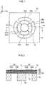
- Figure 1 is a plan view illustrating a configuration of an angular velocity sensor according to one embodiment of the present invention
- Figure 2 is a cross-sectional view taken along a line 2-2 of Figure 1 .
- the angular velocity sensor 10 includes a diaphragm part 12 having an outer circumferential shape that is circular in a plan view, a weight section 14 supported at the central part of the diaphragm part 12, and a pedestal section 16 supporting the outer circumference of the diaphragm part 12.
- the diaphragm part 12 has a laminated structure (multilayer structure) formed by lamination including a vibration plate layer 20, a lower electrode 30, a piezoelectric layer 32, and an upper electrode 34 in this order from the side on which the weight section 14 is joined (a lower surface side in Figure 2 ) in a direction away from the weight section 14 in a film thickness direction (an upward direction of Figure 2 ).
- the diaphragm part 12 is flexible, and the whole circumference of the outer circumference thereof is fixed to the pedestal section 16.
- the vibration plate layer 20 is configured by one or more thin films formed using a thin film forming technique.
- the vibration plate layer 20 having a two-layer structure is illustrated, the vibration plate layer 20 being formed by laminating a second vibration plate layer 22 on the first vibration plate layer 21 (see Figure 2 ), the structure of the vibration plate layer 20 is not limited to this example.
- the vibration plate layer 20 can be configured by a single layer, and may be configured by a laminated structure (multilayer thin film) of two or more layers.
- the thin film forming technique includes a physical gas phase film forming method (PVD: physical vapor deposition), a chemical gas phase film forming method (CVD: chemical vapor deposition), a liquid phase film forming method (plating, application, sol-gel method, spin coat method, etc.), and a thermal oxidation method.
- PVD physical gas phase film forming method
- CVD chemical gas phase film forming method
- liquid phase film forming method plating, application, sol-gel method, spin coat method, etc.
- An appropriate one of the film forming techniques is selected for each layer.
- the term "on” is expressed as “on” with reference to the direction away in the thickness direction from a surface of a member serving as the reference (for example, A) in order to describe the upward-and-downward relationship of the laminated structure without confusion.
- the expression "laminating B on A” is not limited to laminating B directly upon A such that B is in contact with A, but may refer to a case where B is laminated on A via another layer or a plurality of other layers such that the other layer or layers reside between A and B.
- film forming on a substrate (silicon substrate) constituting the pedestal section 16 and the weight section 14 is performed in order of the first vibration plate layer 21, the second vibration plate layer 22, the lower electrode 30, the piezoelectric layer 32, and the upper electrode 34.
- the upper electrode 34 formed on the piezoelectric layer 32 is subjected to patterning so as to include driving electrode parts 35A to 35D functioning as electrodes for use in driving and detection electrode parts 36A to 36D functioning as electrodes for use in detection (see Figure 1 ).
- driving electrode parts 35A to 35D and the detection electrode parts 36A to 36D are each allowed to function as an independent electrode
- each of the electrode parts (35A to 35D and 36A to 36D) are pattern-arranged in a form in which they are discrete from each other.
- the electrode pattern is rotation symmetric about a symmetry axis coinciding with a central axis C L passing the center of the circle of the diaphragm part 12 having an outer circumferential shape that is circular in a plan view.
- the weight section 14 is arranged at a concentric position sharing the central axis C L with the diaphragm part 12.
- the pattern arrangement of the driving electrode parts 35A to 35D and the detection electrode parts 36A to 36D illustrated in Figure 1 is an illustration of four-fold symmetry pattern in which when they are rotated by 90 degrees about the central axis C L , they overlaps with the corresponding other one of them, but the form of the pattern arrangement of the upper electrode 34 is not limited to the example of Figure 1 , and may be provided in various forms of arrangement.
- a piezoelectric element part for use in driving is constituted by the region of the piezoelectric layer 32 residing between the driving electrode parts 35A to 35D and the lower electrode 30.
- a driving voltage is applied between the electrodes of the piezoelectric element part for use in driving (by application of an electric field to the piezoelectric layer 32)
- the diaphragm part 12 and the weight section 14 can be made to vibrate by an inverse piezoelectric effect of the piezoelectric body.
- the piezoelectric element part for use in driving including the driving electrode parts 35A to 35D is connected to a not-shown power source (driving circuit) that supplies a driving electric power, and thereby functions as an energizing unit adapted to make the weight section 14 vibrate.
- a piezoelectric element part for use in detection is constituted by a region of the piezoelectric layer 32 residing between the detection electrode part 36 and the lower electrode 30.
- a Coriolis force acts and causes displacement in the vibration of the weight section 14.
- the displacement caused on the basis of the Coriolis force and generated in the weight section 14 is detected by the piezoelectric effect of the piezoelectric body, and an electric signal (detection signal) is obtained from the detection electrode part 36.
- the piezoelectric element part for use in detection including the detection electrode parts 36A to 36D is connected to a not-shown processing circuit (detection circuit) for processing the detection signal and thereby functions as a displacement detection unit for detecting the displacement of the weight section 14 through.
- a processing circuit detection circuit for processing the detection signal and thereby functions as a displacement detection unit for detecting the displacement of the weight section 14 through.
- an orthogonal XYZ-axes are introduced wherein the center of the circle of the diaphragm part 12 is defined as an origin, a right-left direction of Figure 1 is defined as an X-axis direction, a longitudinal direction of Figure 1 orthogonal thereto is defined as a Y-axis direction, and a vertical direction with respect to the paper surface of Figure 1 is defined as a Z-axis direction.
- the central axis C L illustrated in Figure 2 is an axis parallel to the Z-axis.
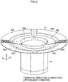
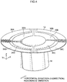
- Figure 3 is a schematic diagram illustrating a state at the time of resonance vibration driving in the Z-direction
- Figure 4 is a schematic diagram illustrating a state at the time of resonance vibration driving in the X-direction. Note that, in Figures 3 and 4 , illustration of the pedestal section 16 is omitted and only the diaphragm part 12 and the weight section 14 are illustrated.
- the flexible diaphragm part 12 When the weight section 14 is resonance-driven in the vertical direction (Z-direction) with respect to the surface of the diaphragm part 12 as illustrated in Figure 3 , the flexible diaphragm part 12 is displaced in the Z-direction, so that a detection signal can be obtained from the detection electrode parts 36A to 36D in response to the displacement.
- the detection principle of the angular velocity is as described in PTL 1 and PTL 2, and with regard to the method of driving the diaphragm part 12, the method described in PTL 1 and the method described in PTL 2 can be adopted.
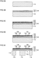
- FIGS. 5A to Figure 5E are explanatory drawings of the manufacturing method of the angular velocity sensor according to this embodiment.
- Step 1 First, a silicon (Si) substrate 110 is prepared (see Figure 5A ).
- Si substrate 110 for use an SOI substrate is not used but a conventional silicon wafer is used, which is less expensive than the SOI substrate.
- Step 2 Next, one or more vibration plate layers 120 are formed on one side surface of the Si substrate 110 by a thin film forming technique such as gas phase film forming (a "vibration plate layer film-forming step").
- a vibration plate layer film-forming step there is illustrated a vibration plate layer having a two-layer structure by forming a first vibration plate layer 121 on the side proximate to the Si substrate 110 and then forming a second vibration plate layer 122 on the first vibration plate layer 121 in a stacked manner, but the vibration plate layer 120 may only include one single layer, or may be configured by a laminated structure of two layer or a more number of layers.
- Step 3 Next, a lower electrode 130 is formed on the vibration plate layer 120 (a "lower electrode forming step").
- Step 4 Next, a piezoelectric layer 132 is formed on the lower electrode 130 (a "piezoelectric layer film-forming step").
- the piezoelectric layer 132 is formed, for example, by a sputtering method.
- Step 5 Next, an upper electrode 134 is formed on the piezoelectric layer 132. As the upper electrode 134, patterning of a driving electrode part 135 and a detection electrode part 156 is performed (see Figure 5D ; an "upper electrode forming step").
- Step 6 Thereafter, a portion of the Si substrate 110 is subjected to a removal process by deep-etching the Si substrate 110 from the rear surface side thereof, and a weight section 114 and a pedestal section 116 are formed by the remaining portion ( Figure 5E ; a "substrate working step").
- the substrate working step the circumference of the weight section 114 is removed such that a groove with a circular ring shape is formed, and the removed portion constitutes a region functioning as the driving part and the detection part of the diaphragm part 112.
- Figures 6A to 6D are explanatory drawings of the manufacturing process of the angular velocity sensor using the SOI substrate.
- an SOI substrate 600 is a multilayer-structure substrate in which a SiO 2 layer 606 is inserted between a silicon substrate as a handle layer 602 and a surface silicon layer 604 (which is referred to as a "device layer").
- the device layer 604 is a layer that is eventually made to function as a vibration plate of the diaphragm part, whose film thickness is adjusted by polishing.
- a lower electrode 630 is formed on the device layer 604 of the SOI substrate 600 as illustrated in Figure 6B , and a piezoelectric layer 632 is formed thereupon.
- a portion of the handle layer 602 is removed by performing deep-etching of the handle layer 602, and a weight section 614 and a pedestal section 616 are formed by the remaining portion.
- the device layer 604 remaining on the portion that has been removed by the deep-etching (reference numeral 612) serves as a vibration plate.
- a vibration plate layer is formed using an inexpensive Si substrate and by a thin film formed by a thin film forming technique, so that manufacturing at lower cost is possible, a thin-film vibration plate layer having less manufacture irregularity can be obtained, and further miniaturization of the device is possible.
- the film thickness of the vibration plate layer can be configured to be 5 micrometers or less.
- the total film thickness of the vibration plate portion constituted by multiple layers including one or more vibration plate layer and a lower electrode can be configured to be 5 micrometers or less.
- designing of resonance frequency is very important.
- designing of the device is generally performed on the basis of calculation of a resonance frequency of a resonance vibration mode for use in either of gyro driving and detection, the calculation being performed using a simulation method such as a finite element method (FEM) from the dimensions of a structural body and an elastic parameter of a material constituting the structural body.
- FEM finite element method
- the first term of the right side of the expression (6) is a resonance frequency when a tension does not act, which is a design value calculated using a finite element method (FEM) or the like.
- FEM finite element method
- T/m in the expression (6) corresponds to T eff which will be later described.
- T eff r ⁇ p t p + ⁇ n ⁇ n t n M
- the mass of the weight section is M (in units of milligrams [mg])
- a circumferential length of the diaphragm part is r (in units of meters [m])
- a stress acting upon the piezoelectric layer is ⁇ p (in units of pascals [Pa])
- a film thickness of the piezoelectric layer is t p (in units of meters [m])
- a stress acting upon an n-th layer counted from the side of the weight section in the vibration plate portion constituted by the lower electrode and one or more vibration plate layer is ⁇ n (in units of pascals [Pa])
- the film thickness of this n-th layer is t n (in units of meters [m]) (where n is a natural number).
- the vibration plate portion in the definition of T eff expressed by the expression (7) includes the lower electrode (common electrode).
- Figure 7 illustrates a schematic diagram illustrating an example of each of the parameters indicated in the expression (7).
- the third vibration plate layer 123 in Figure 7 corresponds to the lower electrode 130 described with reference to Figure 2 .
- a vibration plate portion 150 is constituted by the first vibration plate layer 121, the second vibration plate layer 122, and the third vibration plate layer 123.
- the laminated body of the vibration plate layers (121, 122) and the lower electrode 130 is treated as the "vibration plate portion.”
- illustration is made, supposing that ⁇ 1 is a residual stress in a tensile direction in the first vibration plate layer 121, ⁇ 2 is a residual stress in the compression direction in the second vibration plate layer 122, ⁇ 3 is a residual stress in the tensile direction in the third vibration plate layer 123, and ⁇ P is a residual stress in the tensile direction in the piezoelectric layer 132, wherein the arrows in the figure indicate a direction and a magnitude of the stress acting upon each layer.
- T eff can be readily obtained by calculating ⁇ ave using the expressions (10) and (11) described below.
- ⁇ ave E s t s 2 6 1 ⁇ v t total R '
- R ' 1 1 R 2 ⁇ 1 R 1
- Figures 8A to 8C and Figures 9A to 9D are explanatory drawings of definitions of each of the parameters.
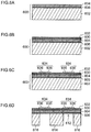
- Figures 8A to 8C are the explanatory drawings of the definitions of R 1 and R 2 according to a first case
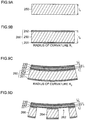
- Figures 9A to 9D are the explanatory drawings of the definitions of R 1 and R 2 according to a second case.
- a case is illustrated in which the vibration plate portion is configured by a two-layer structure, but the same explanation applies to cases in which the vibration plate portion is configured by a layer structure of further multiple layers.
- the first case illustrated in Figures 8A to 8C is a case in which, for example, a single-crystal silicon wafer is used as a substrate 210.
- a plate thickness of the substrate 210 is given as ts.
- a first vibration plate layer 221, a second vibration plate layer 222, and a piezoelectric layer 230 are formed in this order on this substrate 210.
- a film thickness of the first vibration plate layer 221 is ti
- a film thickness of the second vibration plate layer 222 is t 2
- a film thickness of the piezoelectric layer 230 is t P .
- the second vibration plate layer 222 is a layer that corresponds to the lower electrode.
- a pattern-arranged upper electrode is formed on the piezoelectric layer 230.
- a portion of the substrate 210 is removed by deep etching from a rear surface side of the substrate 210, and a weight section 214 and a pedestal section 216 are formed by the remaining portion thereof.
- the part where the silicon layer is removed serves as a driving part and a detection part of a diaphragm part 212.
- a radius of curvature of the substrate 210 in an initial state ( Figure 8A ) prior to film-forming of the first vibration plate layer 221 is given as R 1
- a radius of curvature of a laminated structural body in a state ( Figure 8B ) prior to deep etching following the film-forming of each of the layers (221, 222, 230) of the piezoelectric layer 230 is given as R 2 .
- Es in the expression (10) is a Young's modulus of the substrate 210.
- v is a Poisson's ratio.
- the second case illustrated in Figures 9A to 9D is a case where a film layer that is not eventually configured as the vibration plate is included.
- a base material 250 which serves as a base is used, and for this base material 250, as illustrated in Figure 9B , film layers 251 and 252 that do not eventually become a vibration plate are added to one side surface or both side surfaces of the base material 250 ( Figure 9B ).
- Figure 9B an example is illustrated in which the film layers 251 and 252 are provided on the lower surface and the upper surface of the base material 250, respectively, but a form is possible according to which the film layer is only provided on either one of the surfaces (one side surface).
- a radius of curvature measured in the state of a laminated body 260 of the film layers 251, 252 and the base material 250 is given as R 1 .
- the laminated body 260 of Figure 9B is identified as a member corresponding to the substrate 210 of Figure 8A . Es in this case represents a Young's modulus of the laminated body 260 as a whole.
- the first vibration plate layer 221, the second vibration plate layer 222, and the piezoelectric layer 230 are formed in this order on the film layer 252 of the laminated body 260.
- the pattern-arranged upper electrode is formed on the piezoelectric layer 230.
- a portion of the laminated body 260 is removed by deep etching from a rear surface side (the side of the film layer 251) of the laminated body 260, and a weight section 264 and a pedestal section 266 are formed by the remaining portion thereof.
- the part where the film layers 251, 252 and the base material 250 are removed serves as a driving part and a detection part of a diaphragm part 262.
- the film layers 251 and 252 do not eventually become the vibration plate of the diaphragm part 262.
- a radius of curvature of the base body (laminated body 260) in an initial state ( Figure 9B ) prior to film-forming of the first vibration plate layer 221 is given as R 1
- a radius of curvature of the laminated structural body in the state ( Figure 9C ) prior to deep etching following film-forming of each of the layers (221, 222, 230) of the piezoelectric layer 230 is given as R 2 .
- the term "substrate” in the context of the definition of the radius of curvature R 1 refers to the base body (laminated structural body) in a state where when a film layer or layers that do not eventually become the vibration plate are included, the film layers are all added thereto.
- the radiuses of curvature R 1 and R 2 are defined such that they take a positive (+) value when the surface on the side where the vibration plate layer is formed is in a concave state, and negative (-) value when the surface is in a convex state.
- An average stress ⁇ ave of the composite film can be calculated using the parameters described with reference to Figures 8A to 8C and Figures 9A to 9D .
- the structure in an angular velocity sensor having a structure in which a weight section is supported by a flexible diaphragm part, the structure is made such that there is provided more than one vibration plate layer formed on a silicon substrate by a thin film forming technique such as gas phase film forming.
- a thin film forming technique such as gas phase film forming
- Figure 10 is a plan view illustrating the structure of a prototype angular velocity sensor in accordance with exemplary experiments
- Figure 11 is a cross-sectional view taken along a line 11-11 of Figure 10.
- Figures 10 and 11 are each the same structure described with reference to Figures 1 and 2 , respectively, and with regard to the definition of the dimensions of the device of the later-described each exemplary experiment, as illustrated in Figures 10 and 11 , the outer diameter (major axis in the case of an ellipse) of the diaphragm part 12 is given as ⁇ d , the outer diameter (major axis in the case of an ellipse) of the weight section 14 is given as ⁇ m , and the thickness of the weight section 14 is given as h.
- the circumferential length r is expressed as ⁇ ⁇ ⁇ d .
- Vibration plate layers 1, 2, and 3 were formed on a Si substrate having a thickness h (in units of micrometers [ ⁇ m]) with various gas phase film forming methods.
- the "vibration plate layer 1" corresponds to the first vibration plate layer (the reference numeral 21 of Figure 2 and the reference numeral 121 of Figure 5E )
- the "vibration plate layer 2" corresponds to the second vibration plate layer (the reference numeral 22 of Figure 2 and the reference numeral 122 of Figure 5E )
- the "vibration plate layer 3" corresponds to the lower electrode (the reference numeral 30 of Figure 2 and the reference numeral 130 of Figure 5E , the third vibration plate layer) (see Figures 2 and 5E ).
- a piezoelectric-body (lead zirconate titanate, PZT) film was formed using a high frequency (Rf; radio frequency) sputter device.
- Rf radio frequency
- the film-forming gas 97.5% Ar and 2.5% O 2 were used, and as the target material, that having the composition of Pb 1.3 ((Zr 0.52 Ti 0.48 ) 0.88 Nb 0.12 )O 3 was used.
- a film-forming pressure was 2.2 mTorr (approximately 0.293 Pa), a film-forming temperature was 450°C.
- the obtained PZT film was a Nb-doped PZT thin film in which Nb was added by an atomic composition ratio of 12%.
- an upper electrode in accordance with a layer structure of Au/Ti was pattern-formed by a lift-off method, and eventually a handle layer (silicon substrate layer) was formed by deep etching (Deep RIE) from a back surface of the Si substrate, and thus an angular velocity sensor of the configuration like that of Figures 10 and 11 was created.
- a handle layer silicon substrate layer
- Deep RIE deep etching
- a radius of curvature (R 2 ) of the substrate as a whole was measured, and from this value, an average stress ⁇ ave of the composition film combining the vibration plate layer (vibration plate portion) and the piezoelectric layer was calculated.
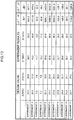
- a resonance frequency (design value) of the resonance vibration mode for use in either one of driving of gyro and detection was calculated using a finite element method from the dimensions of the device structural body and the elastic parameters of the materials constituting the structural body, and the design values and amounts of deviation of the values of resonance frequencies obtained in the actual driving experiments are recorded in the table of Figure 13 .
- the "design value" in this context corresponds to the first term of the right side of the expression (6).
- a design value of a resonance frequency in Z-direction resonance driving is given as "fz”
- a design value of a resonance frequency in X-direction resonance driving is given as “fx”
- the Z-direction resonance frequency and the X-direction resonance frequency that were obtained from the results of the experiments are given as “fz”' and "fx',” respectively.
- Figure 14 is a figure in which relationships between T eff and the difference of squares of the resonance frequency ( ⁇ f 2 ) are plotted from the results of the exemplary experiments 1 to 11.
- the plot points indicated by a black dot represent ⁇ fz 2
- the plot points indicated by a white outline rhombus represent ⁇ fx 2 .
- ⁇ f 2 has a proportional relationship with T eff and that the difference of squares ⁇ fz 2 of the resonance frequency of a vibration mode (referred to as Z-resonance) in which the weight section makes translational vibration in the vertical direction (Z-direction, i.e., in the "film thickness direction") is more susceptible to the effect of T eff .
- Z-resonance the difference of squares ⁇ fz 2 of the resonance frequency of a vibration mode in which the weight section makes translational vibration in the vertical direction (Z-direction, i.e., in the "film thickness direction”
- the shift of the resonance frequency from the design value can be suppressed within the allowable range (here, the resonance frequency shift within 20%) by performing film-forming of each layer by adjusting ⁇ P , ⁇ n , t n , and t P such that the expression (15) is satisfied.
- a resonance frequency shift within 20% of the design value is generally allowable.
- the resonance frequency shift is suppressed within 15% of the design value. More preferably, it is preferable that the resonance frequency shift is suppressed within 10% of the design value.
- the shift of the resonance frequency from the design value can be suppressed within the allowable range (here, the resonance frequency shift within 15%) by performing film-forming of each layer by adjusting ⁇ P , ⁇ n , t n , and t P such that the expression (16) is satisfied.
- the shift of the resonance frequency from the design value can be suppressed within the allowable range (here, the resonance frequency shift within 10%) by performing film-forming of each layer by adjusting, ⁇ P , ⁇ n , t n , and t P such that the expression (17) is satisfied.
- the diaphragm diameter ⁇ d being 1000 micrometers ( ⁇ m) or less, but by virtue of application of the present invention, as illustrated in the exemplary experiments 8 to 10, the diaphragm diameter ⁇ d can be made as small as 800 ⁇ m (exemplary experiment 8) and 700 ⁇ m (exemplary experiments 9, 10).
- the exemplary experiments 8 to 10 are particularly preferable embodiments in terms of miniaturization of the device and suppression of the amount of shift of the resonance frequency from the design value.
- a device layer that becomes the principal part of a vibration plate is in principle in a state of no stress, but when residual stress of the piezoelectric-body film formed thereon is large, the value of resonance frequency is shifted relative to the design value, and it may occur that the specification value as a device is not satisfied.
- the film In a case where the piezoelectric-body thin film is a PZT film, the film generally has a residual stress in a tensile direction.
- a stress control layer is inserted as a layer constituting a vibration plate such that T eff calculated from the expression (7) is maintained within the range identified by the expression (15), the expression (16), or the expression (17), it is possible to suppress the amount of shift of resonance frequency within the allowable range.
- thermally oxidized SiO 2 having a compression stress is formed as a stress control layer with a predetermined film thickness on the surface of the device layer (Si-active layer) so as to maintain T eff within the range.
- the one that includes one or more than two perovskite-type oxides (P) expressed by the following expression may be mentioned.
- lead-containing compounds such as lead titanate, lead zirconate titanate (PZT), lead zirconate, lead lanthanum titanate, lead lanthanum zirconate titanate, magnesium niobate-lead zirconium titanate, magnesium niobate-lead zirconium titanate, nickel niobate-lead zirconium titanate, zinc niobate-lead zirconium titanate, and any mixed crystal system thereof; and lead-free compounds such as barium titanate, strontium barium titanate, bismuth sodium titanate, bismuth potassium titanate, sodium niobate, potassium niobate, lithium niobate, bismuth ferrite, and any mixed crystal system thereof, are mentioned.
- PZT lead zirconate titanate
- lead lanthanum titanate lead lanthanum zirconate titanate
- magnesium niobate-lead zirconium titanate magnesium
- the piezoelectric-body film of this embodiment includes one or more than two perovskite-type oxides (PX) expressed by the following expression: General expression A a (Zr x , Ti y , M b-x-y ) b O c ... (PX).
- the perovskite-type oxide (PX) is an intrinsic PZT, or a PZT whose B-site is partly substituted by M. It is known that a characteristic such as piezoelectric performance are increased, when compared with an intrinsic PZT, in PZTs to which various donor ions having a larger valence number than the valence number of a substitutable ion are added. It is preferable that M is one or more than two donor ions whose valence number is larger than that of tetravalent Zr and Ti. As donor ions of this kind, V 5+ , Nb 5+ , Ta 5+ , Sb 5+ , Mo 6+ , and W 6+ are mentioned.
- b - x - y there is not a particular limitation regarding b - x - y as long as it falls within the range in which the perovskite structure is obtained.
- M is Nb
- the mol ratio of Nb/(Zr + Ti + Nb) is 0.05 or more and 0.25 or less, and more preferably 0.06 or more and 0.20 or less.
- a piezoelectric-body film constituted by a perovskite-type oxide expressed by the above-described general expressions (P) and (PX) has a high piezoelectric distortion constant (d31 constant)
- a piezoelectric element including a piezoelectric-body film like this has a superior displacement characteristic and a detection characteristic.
- a piezoelectric element including a piezoelectric-body film constituted by the perovskite-type oxide expressed by the general expressions (P) and (PX) has voltage-displacement characteristics with superior linearity.
- These piezoelectric materials are the ones that exhibit actuator characteristics and sensor characteristics effective in working of the present invention.
- the perovskite-type oxide expressed by general expression (PX) has a piezoelectric constant higher than that of the one expressed by general expression (P).
- the piezoelectric layer 32 in this embodiment for example, a lead zirconate titanate (PZT) thin film which is doped by Nb at an atomic composition percentage of 12% can be used.
- PZT lead zirconate titanate
- the piezoelectric thin film is directly formed on the substrate by a gas phase growth method and a sol-gel method or the like.
- a thin film has a thickness of 1 ⁇ m or more and 10 ⁇ m or less.
- a gas phase growth method is preferable as the film-forming method of the piezoelectric body.
- various methods may be adopted such as ion plating method, MOCVD method (metalorganic chemical vapor deposition), and PLD method (pulsed laser deposition method).
- MOCVD method metalorganic chemical vapor deposition
- PLD method pulsed laser deposition method
- use of methods other than the gas phase growth method may be contemplated (for example, sol-gel method and the like).
- the piezoelectric-body thin film obtained in this manner is readily subjected to fine processing by etching or the like, and can be patterned in a desired shape. By virtue of this, yield is considerably improved and it is made possible to respond to further device miniaturization.
- substrate materials, electrode materials, piezoelectric materials, film thicknesses, film-forming conditions, and the like may be selected as appropriate in accordance with the purposes.
- diaphragm part that has the circular shape in a plan view has been described with reference to Figure 1 , but the shape is not limited to the circular shape and other configurations are possible such as a diaphragm part in an elliptical shape in a plan view and a diaphragm part in a polygonal shape in a plan view.
- 10 angular velocity sensor
- 12 diaphragm part
- 14 weight section
- 16 pedestal section
- 20 vibration plate layer
- 21 the first vibration plate layer
- 22 the second vibration plate layer
- 30 lower electrode
- 32 piezoelectric layer
- 34 upper electrode
- 35A to 35D driving electrode part
- 36A to 36D detection electrode part
- 110 silicon (Si) substrate
- 112 diaphragm part
- 114 weight section
- 116 pedestal section
- 120 vibration plate layer
- 121 the first vibration plate layer
- 122 the second vibration plate layer
- 123 the third vibration plate layer
- 130 lower electrode
- 132 piezoelectric layer
- 134 upper electrode
- 135 driving electrode part
- 136 detection electrode part
- 150 vibration plate portion
Landscapes
- Engineering & Computer Science (AREA)
- Physics & Mathematics (AREA)
- General Physics & Mathematics (AREA)
- Radar, Positioning & Navigation (AREA)
- Remote Sensing (AREA)
- Manufacturing & Machinery (AREA)
- Gyroscopes (AREA)
Claims (11)
- Capteur de vitesse angulaire (10) comprenant :une partie à diaphragme flexible (12, 112) incluant une structure stratifiée, la structure stratifiée de la partie à diaphragme incluant une électrode supérieure (34, 134), une couche piézoélectrique (32, 132), une électrode inférieure (30, 130), et une ou plusieurs couches de plaques de vibration (20, 21, 22, 120, 121, 122), l'électrode supérieure incluant une partie à électrode de pilotage (35A, 35B, 35C, 35D, 135) et une partie à électrode de détection (36A, 36B,_36C, 36D, 136), la partie à électrode de pilotage et la partie à électrode de détection étant agencées en motifs ;une section socle (16, 116) configurée pour supporter une circonférence extérieure de la partie à diaphragme ; etune section de poids (14, 114) jointe à une partie centrale de la partie à diaphragme,le capteur de vitesse angulaire étant configuré pour amener la section de poids à vibrer en utilisant un effet piézoélectrique inverse d'un corps piézoélectrique par application d'un champ électrique à la couche piézoélectrique via la partie à électrode de pilotage, et détecter un déplacement généré dans la section de poids sur la base d'une force de Coriolis, le déplacement étant détecté par un effet piézoélectrique depuis la partie à électrode de détection,le capteur de vitesse angulaire étant caractérisé en ce que :l'une ou plusieurs couches de plaques de vibration sont formées par une technique de formation de film fin, etTeff est exprimé par l'expression :


- Capteur de vitesse angulaire (10) selon la revendication 1,
dans lequel l'expression suivante est satisfaite :
- Capteur de vitesse angulaire (10) selon la revendication 1,
dans lequel l'expression suivante est satisfaite :
- Capteur de vitesse angulaire (10) selon l'une quelconque des revendications 1 à 3,
dans lequel l'épaisseur de l'une ou plusieurs couches de plaques de vibration est égale à ou inférieure à 5 micromètres. - Capteur de vitesse angulaire (10) selon l'une quelconque des revendications 1 à 4,
dans lequel l'une ou plusieurs couches de plaques de vibration sont des films formés par une formation de film en phase gazeuse. - Capteur de vitesse angulaire (10) selon l'une quelconque des revendications 1 à 5,
dans lequel la couche piézoélectrique est un film fin formé par un procédé de pulvérisation. - Capteur de vitesse angulaire (10) selon l'une quelconque des revendications 1 à 6,
dans lequel la couche piézoélectrique est un ou plus de deux oxydes de type pérovskite exprimés par une expression suivante :
expression générale ABO3 ... (P),
dans laquelle A est un élément de site A qui est au moins un élément incluant Pb ;B est un élément de site B qui est au moins un élément sélectionné parmi un groupe consistant en Ti, Zr, V, Nb, Ta, Sb, Cr, Mo, W, Mn, Sc, Co, Cu, In, Sn, Ga, Zn, Cd, Fe, et Ni ;O est un élément oxygène ; etun rapport molaire de l'élément de site A, l'élément de site B, et l'élément oxygène est 1:1:3 en tant que standard, et le rapport molaire de celui-ci peut être dévié d'un rapport molaire de référence tant qu'une structure de pérovskite est obtenue. - Capteur de vitesse angulaire (10) selon l'une quelconque des revendications 1 à 6,
dans lequel la couche piézoélectrique est un ou plus de deux oxydes de type pérovskite exprimés par une expression suivante (PX) :
Aa(Zrx, Tiy, Mb-x-y)bOc... (PX),
dans laquelle A est un élément de site A qui est au moins un élément incluant Pb ;M est au moins un élément sélectionné parmi un groupe consistant en V, Nb, Ta, et Sb,où0 < x < b ; 0 < y< b, et0 ≤ b-x-y ; etun rapport molaire de a:b:c = 1:1:3 est un standard, et le rapport molaire de celui-ci peut être dévié d'un rapport molaire de référence tant qu'une structure de pérovskite est obtenue. - Capteur de vitesse angulaire (10) selon l'une quelconque des revendications 1 à 8,
dans lequel l'une ou plusieurs couches de plaques de vibration sont obtenues en étant formées sur un substrat de silicium ; et
la section de poids et la section socle sont configurées par des portions restantes du substrat de silicium, les portions restantes étant obtenues à la suite de l'enlèvement d'une partie du substrat de silicium ayant la couche de plaque de vibration formée sur celle-ci. - Capteur de vitesse angulaire (10) selon l'une quelconque des revendications 1 à 8,
dans lequel la partie à diaphragme présente une forme circonférentielle extérieure qui est une forme circulaire ou une forme elliptique dans une vue en plan ; et
la section de poids est disposée à une position concentrique de la forme circulaire ou la forme elliptique partageant un axe central avec la partie à diaphragme. - Procédé de fabrication d'un capteur de vitesse angulaire (10), le capteur de vitesse angulaire incluant une partie à diaphragme flexible (12, 112) incluant une structure stratifiée, la structure stratifiée de la partie à diaphragme incluant une électrode supérieure (34, 134), une couche piézoélectrique (32, 132), une électrode inférieure (30, 130), et une ou plusieurs couches de plaques de vibration (20, 21, 22, 120, 121, 122), l'électrode supérieure incluant une partie à électrode de pilotage (35A, 35B, 35C, 35D, 135) et une partie à électrode de détection (36A, 36B, 36C, 36D, 136), la partie à électrode de pilotage et la partie à électrode de détection étant agencées en motifs ;
une section socle (16, 116) configurée pour supporter une circonférence extérieure de la partie à diaphragme ; et
une section de poids (14, 114) jointe à une partie centrale de la partie à diaphragme,
le capteur de vitesse angulaire étant configuré pour amener la section de poids à vibrer en utilisant un effet piézoélectrique inverse d'un corps piézoélectrique par application d'un champ électrique à la couche piézoélectrique via la partie à électrode de pilotage, et détecter un déplacement généré dans la section de poids sur la base d'une force de Coriolis, le déplacement étant détecté par un effet piézoélectrique depuis la partie à électrode de détection ;
le procédé comprenant :une formation de l'une ou plusieurs couches de plaques de vibration en utilisant une technique de formation de film fin ; etun ajustage de σP, σn, tn, et tP de sorte que Teff exprimé par l'expression :

Applications Claiming Priority (2)
| Application Number | Priority Date | Filing Date | Title |
|---|---|---|---|
| JP2013019736A JP5988494B2 (ja) | 2013-02-04 | 2013-02-04 | 角速度センサ及びその製造方法 |
| PCT/JP2014/051929 WO2014119609A1 (fr) | 2013-02-04 | 2014-01-29 | Capteur de vitesse angulaire et procédé de fabrication associé |
Publications (3)
| Publication Number | Publication Date |
|---|---|
| EP2952853A1 EP2952853A1 (fr) | 2015-12-09 |
| EP2952853A4 EP2952853A4 (fr) | 2016-02-10 |
| EP2952853B1 true EP2952853B1 (fr) | 2018-04-04 |
Family
ID=51262322
Family Applications (1)
| Application Number | Title | Priority Date | Filing Date |
|---|---|---|---|
| EP14746045.5A Not-in-force EP2952853B1 (fr) | 2013-02-04 | 2014-01-29 | Capteur de vitesse angulaire et procédé de fabrication associé |
Country Status (6)
| Country | Link |
|---|---|
| US (1) | US9702698B2 (fr) |
| EP (1) | EP2952853B1 (fr) |
| JP (1) | JP5988494B2 (fr) |
| CN (1) | CN104995484B (fr) |
| TW (1) | TW201432221A (fr) |
| WO (1) | WO2014119609A1 (fr) |
Families Citing this family (11)
| Publication number | Priority date | Publication date | Assignee | Title |
|---|---|---|---|---|
| WO2014155997A1 (fr) * | 2013-03-29 | 2014-10-02 | 旭化成株式会社 | Capteur de vitesse angulaire |
| JPWO2014178172A1 (ja) * | 2013-04-30 | 2017-02-23 | 旭化成株式会社 | 角速度センサ |
| KR101516112B1 (ko) * | 2014-01-29 | 2015-04-29 | 삼성전기주식회사 | Mems 센서 |
| US9970831B2 (en) | 2014-02-10 | 2018-05-15 | Texas Instruments Incorporated | Piezoelectric thin-film sensor |
| US10353503B2 (en) | 2015-10-29 | 2019-07-16 | Texas Instruments Incorporated | Integrated force sensing element |
| US9879996B2 (en) * | 2015-11-30 | 2018-01-30 | General Electric Company | System and method of electrostatic carouseling for gyrocompassing |
| CN106441260B (zh) * | 2016-08-23 | 2020-12-01 | 上海交通大学 | 硅上压电薄膜多支撑梁mems陀螺及其制备方法 |
| US10655964B2 (en) * | 2017-08-08 | 2020-05-19 | Hrl Laboratories, Llc | High quality factor MEMS silicon flower-of-life vibratory gyroscope |
| JP2021067624A (ja) * | 2019-10-28 | 2021-04-30 | セイコーエプソン株式会社 | 慣性計測装置、電子機器及び移動体 |
| US10999684B1 (en) | 2020-01-17 | 2021-05-04 | Sae Magnetics (H.K.) Ltd. | MEMS microphone and method of manufacturing the MEMS microphone |
| CN114666717B (zh) * | 2022-05-24 | 2022-08-26 | 武汉敏声新技术有限公司 | 压电mems麦克风芯片及压电mems麦克风 |
Family Cites Families (19)
| Publication number | Priority date | Publication date | Assignee | Title |
|---|---|---|---|---|
| JPS6147277A (ja) | 1984-08-11 | 1986-03-07 | Erumu:Kk | インクジエツト式記録装置 |
| JPH0412232A (ja) | 1990-04-28 | 1992-01-16 | Pentel Kk | 手持型電子計算機端末 |
| US6282956B1 (en) * | 1994-12-29 | 2001-09-04 | Kazuhiro Okada | Multi-axial angular velocity sensor |
| US6747393B2 (en) * | 1996-11-26 | 2004-06-08 | Ngk Insulators, Ltd. | Vibrator, vibratory gyroscope, and vibration adjusting method |
| US20040221651A1 (en) * | 2003-05-08 | 2004-11-11 | Schiller Peter J. | Force balanced piezoelectric rate sensor |
| JP2005345245A (ja) * | 2004-06-02 | 2005-12-15 | Seiko Instruments Inc | 容量型力学量センサ及びその製造方法 |
| JP2006153481A (ja) * | 2004-11-25 | 2006-06-15 | Seiko Instruments Inc | 力学量センサ |
| US7617727B2 (en) * | 2006-04-18 | 2009-11-17 | Watson Industries, Inc. | Vibrating inertial rate sensor utilizing split or skewed operational elements |
| JP4012232B2 (ja) | 2006-04-21 | 2007-11-21 | 株式会社ワコー | 角速度センサ |
| US7493814B2 (en) * | 2006-12-22 | 2009-02-24 | The Boeing Company | Vibratory gyroscope with parasitic mode damping |
| JP4276276B2 (ja) * | 2007-09-07 | 2009-06-10 | 富士フイルム株式会社 | 圧電素子の製造方法 |
| WO2009119205A1 (fr) * | 2008-03-25 | 2009-10-01 | 住友精密工業株式会社 | Gyroscope vibratoire utilisant un film piézoélectrique |
| US20100058861A1 (en) * | 2008-09-11 | 2010-03-11 | Analog Devices, Inc. | Piezoelectric Transducers and Inertial Sensors using Piezoelectric Transducers |
| JP2010071793A (ja) * | 2008-09-18 | 2010-04-02 | Toshiba Corp | 多軸加速度センサ及び角速度センサ |
| JP2010145122A (ja) * | 2008-12-16 | 2010-07-01 | Murata Mfg Co Ltd | 圧電振動子および振動ジャイロ装置 |
| JP5227199B2 (ja) | 2009-01-09 | 2013-07-03 | 株式会社ワコー | 角速度センサ |
| KR101843185B1 (ko) * | 2011-06-20 | 2018-03-29 | 삼성전기주식회사 | 관성센서 |
| WO2012001942A1 (fr) * | 2010-06-30 | 2012-01-05 | パナソニック株式会社 | Tête d'impression à jet d'encre, procédé de formation d'images utilisant ladite tête, capteur de vitesse angulaire, procédé pour déterminer une vitesse angulaire avec ledit capteur, élément piézoélectrique produisant de l'énergie, et procédé de production d'énergie utilisant ledit élément |
| WO2012026107A1 (fr) * | 2010-08-27 | 2012-03-01 | パナソニック株式会社 | Tête à jet d'encre, procédé de formation d'image utilisant une tête à jet d'encre, capteur de vitesse angulaire, procédé de mesure de la vitesse angulaire utilisant un capteur de vitesse angulaire, élément piézoélectrique pour la production d'énergie et procédé de production d'énergie utilisant un élément piézoélectrique pour la production d'énergie |
-
2013
- 2013-02-04 JP JP2013019736A patent/JP5988494B2/ja not_active Expired - Fee Related
-
2014
- 2014-01-29 WO PCT/JP2014/051929 patent/WO2014119609A1/fr not_active Ceased
- 2014-01-29 EP EP14746045.5A patent/EP2952853B1/fr not_active Not-in-force
- 2014-01-29 TW TW103103326A patent/TW201432221A/zh unknown
- 2014-01-29 CN CN201480007198.4A patent/CN104995484B/zh not_active Expired - Fee Related
-
2015
- 2015-07-27 US US14/809,941 patent/US9702698B2/en not_active Expired - Fee Related
Non-Patent Citations (1)
| Title |
|---|
| None * |
Also Published As
| Publication number | Publication date |
|---|---|
| JP5988494B2 (ja) | 2016-09-07 |
| JP2014149278A (ja) | 2014-08-21 |
| CN104995484B (zh) | 2017-07-28 |
| US20150330785A1 (en) | 2015-11-19 |
| WO2014119609A1 (fr) | 2014-08-07 |
| US9702698B2 (en) | 2017-07-11 |
| EP2952853A1 (fr) | 2015-12-09 |
| EP2952853A4 (fr) | 2016-02-10 |
| TW201432221A (zh) | 2014-08-16 |
| CN104995484A (zh) | 2015-10-21 |
Similar Documents
| Publication | Publication Date | Title |
|---|---|---|
| EP2952853B1 (fr) | Capteur de vitesse angulaire et procédé de fabrication associé | |
| EP2539946B1 (fr) | Récolteur d'énergie micro-vibratoire par mems de grande efficacité et procédé de fabrication de celui-ci | |
| JP4600468B2 (ja) | 半導体圧力センサ及びその製造方法、半導体装置並びに電子機器 | |
| US11581827B2 (en) | Energy harvesting with a micro-electro-mechanical system (MEMS) | |
| JP5130422B2 (ja) | 検出センサ | |
| US20080173092A1 (en) | Motion sensor, accelerometer, inclination sensor, pressure sensor, and tactile controller | |
| JP2007071677A (ja) | コンバインドセンサとその製造方法 | |
| US9273962B2 (en) | Physical quantity sensor and electronic device | |
| US20070240511A1 (en) | Angular rate sensor and method of manufacturing the same | |
| US9032795B2 (en) | MEMS resonator, sensor having the same and manufacturing method for MEMS resonator | |
| JP2019053054A (ja) | 自動周波数制御回路用の圧電素子、それを備えた機械振動系および装置、ならびに圧電素子の製造方法 | |
| US20150330782A1 (en) | Mass-loaded coriolis vibratory gyroscope | |
| Wang et al. | Indirect excitation of micro-HRG using segmented piezoelectric ALD PHT actuator | |
| Kanda et al. | Three-dimensional piezoelectric MEMS actuator by using sputtering deposition of Pb (Zr, Ti) O3 on microstructure sidewalls | |
| US10158063B2 (en) | Monolithic PZT actuator, stage, and method for making | |
| JP2010187059A (ja) | ウォーク型振動片およびその製造方法 | |
| US10707405B2 (en) | Electromechanical actuator | |
| JP2009198493A (ja) | 角速度検出装置 | |
| JP6193599B2 (ja) | 角速度センサ及びその製造方法 | |
| JPH10178181A (ja) | 半導体慣性センサの製造方法 | |
| JP6594527B2 (ja) | 複合センサ | |
| JP2017203692A (ja) | 物理量センサーの製造方法および振動素子の周波数調整方法 | |
| Faizan | Design and Fabrication of Multilayer Piezoelectric NEMS Resonators | |
| CN106248068A (zh) | 相邻面双分立电极分布式的微陀螺仪及其制备方法 | |
| CN106323262A (zh) | 内分立外环形的双电极分布式微陀螺仪及其制备方法 |
Legal Events
| Date | Code | Title | Description |
|---|---|---|---|
| PUAI | Public reference made under article 153(3) epc to a published international application that has entered the european phase |
Free format text: ORIGINAL CODE: 0009012 |
|
| 17P | Request for examination filed |
Effective date: 20150717 |
|
| AK | Designated contracting states |
Kind code of ref document: A1 Designated state(s): AL AT BE BG CH CY CZ DE DK EE ES FI FR GB GR HR HU IE IS IT LI LT LU LV MC MK MT NL NO PL PT RO RS SE SI SK SM TR |
|
| AX | Request for extension of the european patent |
Extension state: BA ME |
|
| A4 | Supplementary search report drawn up and despatched |
Effective date: 20160113 |
|
| RIC1 | Information provided on ipc code assigned before grant |
Ipc: G01C 25/00 20060101ALI20160107BHEP Ipc: G01C 19/56 20120101AFI20160107BHEP |
|
| DAX | Request for extension of the european patent (deleted) | ||
| REG | Reference to a national code |
Ref country code: DE Ref legal event code: R079 Ref document number: 602014023354 Country of ref document: DE Free format text: PREVIOUS MAIN CLASS: G01C0019578300 Ipc: G01C0019560000 |
|
| RIC1 | Information provided on ipc code assigned before grant |
Ipc: G01P 15/097 20060101ALI20170725BHEP Ipc: G01P 15/09 20060101ALI20170725BHEP Ipc: G01C 19/56 20120101AFI20170725BHEP Ipc: G01C 25/00 20060101ALI20170725BHEP |
|
| GRAP | Despatch of communication of intention to grant a patent |
Free format text: ORIGINAL CODE: EPIDOSNIGR1 |
|
| STAA | Information on the status of an ep patent application or granted ep patent |
Free format text: STATUS: GRANT OF PATENT IS INTENDED |
|
| INTG | Intention to grant announced |
Effective date: 20171109 |
|
| GRAS | Grant fee paid |
Free format text: ORIGINAL CODE: EPIDOSNIGR3 |
|
| GRAJ | Information related to disapproval of communication of intention to grant by the applicant or resumption of examination proceedings by the epo deleted |
Free format text: ORIGINAL CODE: EPIDOSDIGR1 |
|
| GRAL | Information related to payment of fee for publishing/printing deleted |
Free format text: ORIGINAL CODE: EPIDOSDIGR3 |
|
| STAA | Information on the status of an ep patent application or granted ep patent |
Free format text: STATUS: REQUEST FOR EXAMINATION WAS MADE |
|
| GRAR | Information related to intention to grant a patent recorded |
Free format text: ORIGINAL CODE: EPIDOSNIGR71 |
|
| STAA | Information on the status of an ep patent application or granted ep patent |
Free format text: STATUS: GRANT OF PATENT IS INTENDED |
|
| GRAA | (expected) grant |
Free format text: ORIGINAL CODE: 0009210 |
|
| STAA | Information on the status of an ep patent application or granted ep patent |
Free format text: STATUS: THE PATENT HAS BEEN GRANTED |
|
| INTC | Intention to grant announced (deleted) | ||
| INTG | Intention to grant announced |
Effective date: 20180220 |
|
| AK | Designated contracting states |
Kind code of ref document: B1 Designated state(s): AL AT BE BG CH CY CZ DE DK EE ES FI FR GB GR HR HU IE IS IT LI LT LU LV MC MK MT NL NO PL PT RO RS SE SI SK SM TR |
|
| REG | Reference to a national code |
Ref country code: GB Ref legal event code: FG4D |
|
| REG | Reference to a national code |
Ref country code: CH Ref legal event code: EP |
|
| REG | Reference to a national code |
Ref country code: AT Ref legal event code: REF Ref document number: 986063 Country of ref document: AT Kind code of ref document: T Effective date: 20180415 |
|
| REG | Reference to a national code |
Ref country code: IE Ref legal event code: FG4D |
|
| REG | Reference to a national code |
Ref country code: DE Ref legal event code: R096 Ref document number: 602014023354 Country of ref document: DE |
|
| REG | Reference to a national code |
Ref country code: NL Ref legal event code: MP Effective date: 20180404 |
|
| REG | Reference to a national code |
Ref country code: LT Ref legal event code: MG4D |
|
| PG25 | Lapsed in a contracting state [announced via postgrant information from national office to epo] |
Ref country code: NL Free format text: LAPSE BECAUSE OF FAILURE TO SUBMIT A TRANSLATION OF THE DESCRIPTION OR TO PAY THE FEE WITHIN THE PRESCRIBED TIME-LIMIT Effective date: 20180404 |
|
| PG25 | Lapsed in a contracting state [announced via postgrant information from national office to epo] |
Ref country code: BG Free format text: LAPSE BECAUSE OF FAILURE TO SUBMIT A TRANSLATION OF THE DESCRIPTION OR TO PAY THE FEE WITHIN THE PRESCRIBED TIME-LIMIT Effective date: 20180704 Ref country code: FI Free format text: LAPSE BECAUSE OF FAILURE TO SUBMIT A TRANSLATION OF THE DESCRIPTION OR TO PAY THE FEE WITHIN THE PRESCRIBED TIME-LIMIT Effective date: 20180404 Ref country code: NO Free format text: LAPSE BECAUSE OF FAILURE TO SUBMIT A TRANSLATION OF THE DESCRIPTION OR TO PAY THE FEE WITHIN THE PRESCRIBED TIME-LIMIT Effective date: 20180704 Ref country code: ES Free format text: LAPSE BECAUSE OF FAILURE TO SUBMIT A TRANSLATION OF THE DESCRIPTION OR TO PAY THE FEE WITHIN THE PRESCRIBED TIME-LIMIT Effective date: 20180404 Ref country code: AL Free format text: LAPSE BECAUSE OF FAILURE TO SUBMIT A TRANSLATION OF THE DESCRIPTION OR TO PAY THE FEE WITHIN THE PRESCRIBED TIME-LIMIT Effective date: 20180404 Ref country code: SE Free format text: LAPSE BECAUSE OF FAILURE TO SUBMIT A TRANSLATION OF THE DESCRIPTION OR TO PAY THE FEE WITHIN THE PRESCRIBED TIME-LIMIT Effective date: 20180404 Ref country code: LT Free format text: LAPSE BECAUSE OF FAILURE TO SUBMIT A TRANSLATION OF THE DESCRIPTION OR TO PAY THE FEE WITHIN THE PRESCRIBED TIME-LIMIT Effective date: 20180404 Ref country code: PL Free format text: LAPSE BECAUSE OF FAILURE TO SUBMIT A TRANSLATION OF THE DESCRIPTION OR TO PAY THE FEE WITHIN THE PRESCRIBED TIME-LIMIT Effective date: 20180404 |
|
| PG25 | Lapsed in a contracting state [announced via postgrant information from national office to epo] |
Ref country code: LV Free format text: LAPSE BECAUSE OF FAILURE TO SUBMIT A TRANSLATION OF THE DESCRIPTION OR TO PAY THE FEE WITHIN THE PRESCRIBED TIME-LIMIT Effective date: 20180404 Ref country code: RS Free format text: LAPSE BECAUSE OF FAILURE TO SUBMIT A TRANSLATION OF THE DESCRIPTION OR TO PAY THE FEE WITHIN THE PRESCRIBED TIME-LIMIT Effective date: 20180404 Ref country code: HR Free format text: LAPSE BECAUSE OF FAILURE TO SUBMIT A TRANSLATION OF THE DESCRIPTION OR TO PAY THE FEE WITHIN THE PRESCRIBED TIME-LIMIT Effective date: 20180404 Ref country code: GR Free format text: LAPSE BECAUSE OF FAILURE TO SUBMIT A TRANSLATION OF THE DESCRIPTION OR TO PAY THE FEE WITHIN THE PRESCRIBED TIME-LIMIT Effective date: 20180705 |
|
| REG | Reference to a national code |
Ref country code: AT Ref legal event code: MK05 Ref document number: 986063 Country of ref document: AT Kind code of ref document: T Effective date: 20180404 |
|
| PG25 | Lapsed in a contracting state [announced via postgrant information from national office to epo] |
Ref country code: PT Free format text: LAPSE BECAUSE OF FAILURE TO SUBMIT A TRANSLATION OF THE DESCRIPTION OR TO PAY THE FEE WITHIN THE PRESCRIBED TIME-LIMIT Effective date: 20180806 |
|
| REG | Reference to a national code |
Ref country code: DE Ref legal event code: R097 Ref document number: 602014023354 Country of ref document: DE |
|
| PG25 | Lapsed in a contracting state [announced via postgrant information from national office to epo] |
Ref country code: EE Free format text: LAPSE BECAUSE OF FAILURE TO SUBMIT A TRANSLATION OF THE DESCRIPTION OR TO PAY THE FEE WITHIN THE PRESCRIBED TIME-LIMIT Effective date: 20180404 Ref country code: AT Free format text: LAPSE BECAUSE OF FAILURE TO SUBMIT A TRANSLATION OF THE DESCRIPTION OR TO PAY THE FEE WITHIN THE PRESCRIBED TIME-LIMIT Effective date: 20180404 Ref country code: RO Free format text: LAPSE BECAUSE OF FAILURE TO SUBMIT A TRANSLATION OF THE DESCRIPTION OR TO PAY THE FEE WITHIN THE PRESCRIBED TIME-LIMIT Effective date: 20180404 Ref country code: CZ Free format text: LAPSE BECAUSE OF FAILURE TO SUBMIT A TRANSLATION OF THE DESCRIPTION OR TO PAY THE FEE WITHIN THE PRESCRIBED TIME-LIMIT Effective date: 20180404 Ref country code: SK Free format text: LAPSE BECAUSE OF FAILURE TO SUBMIT A TRANSLATION OF THE DESCRIPTION OR TO PAY THE FEE WITHIN THE PRESCRIBED TIME-LIMIT Effective date: 20180404 Ref country code: DK Free format text: LAPSE BECAUSE OF FAILURE TO SUBMIT A TRANSLATION OF THE DESCRIPTION OR TO PAY THE FEE WITHIN THE PRESCRIBED TIME-LIMIT Effective date: 20180404 |
|
| PLBE | No opposition filed within time limit |
Free format text: ORIGINAL CODE: 0009261 |
|
| STAA | Information on the status of an ep patent application or granted ep patent |
Free format text: STATUS: NO OPPOSITION FILED WITHIN TIME LIMIT |
|
| PG25 | Lapsed in a contracting state [announced via postgrant information from national office to epo] |
Ref country code: SM Free format text: LAPSE BECAUSE OF FAILURE TO SUBMIT A TRANSLATION OF THE DESCRIPTION OR TO PAY THE FEE WITHIN THE PRESCRIBED TIME-LIMIT Effective date: 20180404 Ref country code: IT Free format text: LAPSE BECAUSE OF FAILURE TO SUBMIT A TRANSLATION OF THE DESCRIPTION OR TO PAY THE FEE WITHIN THE PRESCRIBED TIME-LIMIT Effective date: 20180404 |
|
| 26N | No opposition filed |
Effective date: 20190107 |
|
| PG25 | Lapsed in a contracting state [announced via postgrant information from national office to epo] |
Ref country code: SI Free format text: LAPSE BECAUSE OF FAILURE TO SUBMIT A TRANSLATION OF THE DESCRIPTION OR TO PAY THE FEE WITHIN THE PRESCRIBED TIME-LIMIT Effective date: 20180404 |
|
| PG25 | Lapsed in a contracting state [announced via postgrant information from national office to epo] |
Ref country code: MC Free format text: LAPSE BECAUSE OF FAILURE TO SUBMIT A TRANSLATION OF THE DESCRIPTION OR TO PAY THE FEE WITHIN THE PRESCRIBED TIME-LIMIT Effective date: 20180404 |
|
| REG | Reference to a national code |
Ref country code: CH Ref legal event code: PL |
|
| PG25 | Lapsed in a contracting state [announced via postgrant information from national office to epo] |
Ref country code: LU Free format text: LAPSE BECAUSE OF NON-PAYMENT OF DUE FEES Effective date: 20190129 |
|
| REG | Reference to a national code |
Ref country code: BE Ref legal event code: MM Effective date: 20190131 |
|
| REG | Reference to a national code |
Ref country code: IE Ref legal event code: MM4A |
|
| PG25 | Lapsed in a contracting state [announced via postgrant information from national office to epo] |
Ref country code: BE Free format text: LAPSE BECAUSE OF NON-PAYMENT OF DUE FEES Effective date: 20190131 |
|
| PG25 | Lapsed in a contracting state [announced via postgrant information from national office to epo] |
Ref country code: LI Free format text: LAPSE BECAUSE OF NON-PAYMENT OF DUE FEES Effective date: 20190131 Ref country code: CH Free format text: LAPSE BECAUSE OF NON-PAYMENT OF DUE FEES Effective date: 20190131 |
|
| PG25 | Lapsed in a contracting state [announced via postgrant information from national office to epo] |
Ref country code: IE Free format text: LAPSE BECAUSE OF NON-PAYMENT OF DUE FEES Effective date: 20190129 |
|
| PG25 | Lapsed in a contracting state [announced via postgrant information from national office to epo] |
Ref country code: TR Free format text: LAPSE BECAUSE OF FAILURE TO SUBMIT A TRANSLATION OF THE DESCRIPTION OR TO PAY THE FEE WITHIN THE PRESCRIBED TIME-LIMIT Effective date: 20180404 |
|
| PG25 | Lapsed in a contracting state [announced via postgrant information from national office to epo] |
Ref country code: MT Free format text: LAPSE BECAUSE OF NON-PAYMENT OF DUE FEES Effective date: 20190129 |
|
| PGFP | Annual fee paid to national office [announced via postgrant information from national office to epo] |
Ref country code: FR Payment date: 20201210 Year of fee payment: 8 |
|
| PG25 | Lapsed in a contracting state [announced via postgrant information from national office to epo] |
Ref country code: CY Free format text: LAPSE BECAUSE OF FAILURE TO SUBMIT A TRANSLATION OF THE DESCRIPTION OR TO PAY THE FEE WITHIN THE PRESCRIBED TIME-LIMIT Effective date: 20180404 |
|
| PGFP | Annual fee paid to national office [announced via postgrant information from national office to epo] |
Ref country code: GB Payment date: 20210120 Year of fee payment: 8 Ref country code: DE Payment date: 20210119 Year of fee payment: 8 |
|
| PG25 | Lapsed in a contracting state [announced via postgrant information from national office to epo] |
Ref country code: IS Free format text: LAPSE BECAUSE OF FAILURE TO SUBMIT A TRANSLATION OF THE DESCRIPTION OR TO PAY THE FEE WITHIN THE PRESCRIBED TIME-LIMIT Effective date: 20180804 |
|
| PG25 | Lapsed in a contracting state [announced via postgrant information from national office to epo] |
Ref country code: HU Free format text: LAPSE BECAUSE OF FAILURE TO SUBMIT A TRANSLATION OF THE DESCRIPTION OR TO PAY THE FEE WITHIN THE PRESCRIBED TIME-LIMIT; INVALID AB INITIO Effective date: 20140129 |
|
| PG25 | Lapsed in a contracting state [announced via postgrant information from national office to epo] |
Ref country code: MK Free format text: LAPSE BECAUSE OF FAILURE TO SUBMIT A TRANSLATION OF THE DESCRIPTION OR TO PAY THE FEE WITHIN THE PRESCRIBED TIME-LIMIT Effective date: 20180404 |
|
| REG | Reference to a national code |
Ref country code: DE Ref legal event code: R119 Ref document number: 602014023354 Country of ref document: DE |
|
| GBPC | Gb: european patent ceased through non-payment of renewal fee |
Effective date: 20220129 |
|
| PG25 | Lapsed in a contracting state [announced via postgrant information from national office to epo] |
Ref country code: GB Free format text: LAPSE BECAUSE OF NON-PAYMENT OF DUE FEES Effective date: 20220129 Ref country code: DE Free format text: LAPSE BECAUSE OF NON-PAYMENT OF DUE FEES Effective date: 20220802 |
|
| PG25 | Lapsed in a contracting state [announced via postgrant information from national office to epo] |
Ref country code: FR Free format text: LAPSE BECAUSE OF NON-PAYMENT OF DUE FEES Effective date: 20220131 |