EP3208231B1 - Verfahren zur herstellung einer al/ge-verbindung im bereich der waferverkapselung - Google Patents
Verfahren zur herstellung einer al/ge-verbindung im bereich der waferverkapselung Download PDFInfo
- Publication number
- EP3208231B1 EP3208231B1 EP17161696.4A EP17161696A EP3208231B1 EP 3208231 B1 EP3208231 B1 EP 3208231B1 EP 17161696 A EP17161696 A EP 17161696A EP 3208231 B1 EP3208231 B1 EP 3208231B1
- Authority
- EP
- European Patent Office
- Prior art keywords
- substrate wafer
- wafer
- substrate
- aluminum
- germanium
- Prior art date
- Legal status (The legal status is an assumption and is not a legal conclusion. Google has not performed a legal analysis and makes no representation as to the accuracy of the status listed.)
- Expired - Lifetime
Links
Images


Classifications
-
- H—ELECTRICITY
- H10—SEMICONDUCTOR DEVICES; ELECTRIC SOLID-STATE DEVICES NOT OTHERWISE PROVIDED FOR
- H10W—GENERIC PACKAGES, INTERCONNECTIONS, CONNECTORS OR OTHER CONSTRUCTIONAL DETAILS OF DEVICES COVERED BY CLASS H10
- H10W95/00—Packaging processes not covered by the other groups of this subclass
-
- H—ELECTRICITY
- H10—SEMICONDUCTOR DEVICES; ELECTRIC SOLID-STATE DEVICES NOT OTHERWISE PROVIDED FOR
- H10W—GENERIC PACKAGES, INTERCONNECTIONS, CONNECTORS OR OTHER CONSTRUCTIONAL DETAILS OF DEVICES COVERED BY CLASS H10
- H10W72/00—Interconnections or connectors in packages
- H10W72/20—Bump connectors, e.g. solder bumps or copper pillars; Dummy bumps; Thermal bumps
-
- B—PERFORMING OPERATIONS; TRANSPORTING
- B81—MICROSTRUCTURAL TECHNOLOGY
- B81C—PROCESSES OR APPARATUS SPECIALLY ADAPTED FOR THE MANUFACTURE OR TREATMENT OF MICROSTRUCTURAL DEVICES OR SYSTEMS
- B81C1/00—Manufacture or treatment of devices or systems in or on a substrate
- B81C1/00015—Manufacture or treatment of devices or systems in or on a substrate for manufacturing microsystems
- B81C1/00222—Integrating an electronic processing unit with a micromechanical structure
- B81C1/00238—Joining a substrate with an electronic processing unit and a substrate with a micromechanical structure
-
- B—PERFORMING OPERATIONS; TRANSPORTING
- B23—MACHINE TOOLS; METAL-WORKING NOT OTHERWISE PROVIDED FOR
- B23K—SOLDERING OR UNSOLDERING; WELDING; CLADDING OR PLATING BY SOLDERING OR WELDING; CUTTING BY APPLYING HEAT LOCALLY, e.g. FLAME CUTTING; WORKING BY LASER BEAM
- B23K20/00—Non-electric welding by applying impact or other pressure, with or without the application of heat, e.g. cladding or plating
- B23K20/02—Non-electric welding by applying impact or other pressure, with or without the application of heat, e.g. cladding or plating by means of a press ; Diffusion bonding
- B23K20/023—Thermo-compression bonding
-
- B—PERFORMING OPERATIONS; TRANSPORTING
- B81—MICROSTRUCTURAL TECHNOLOGY
- B81B—MICROSTRUCTURAL DEVICES OR SYSTEMS, e.g. MICROMECHANICAL DEVICES
- B81B3/00—Devices comprising flexible or deformable elements, e.g. comprising elastic tongues or membranes
- B81B3/0018—Structures acting upon the moving or flexible element for transforming energy into mechanical movement or vice versa, i.e. actuators, sensors, generators
-
- B—PERFORMING OPERATIONS; TRANSPORTING
- B81—MICROSTRUCTURAL TECHNOLOGY
- B81B—MICROSTRUCTURAL DEVICES OR SYSTEMS, e.g. MICROMECHANICAL DEVICES
- B81B7/00—Microstructural systems ; Auxiliary parts of microstructural devices or systems
- B81B7/0032—Packages or encapsulation
- B81B7/007—Interconnections between the MEMS and external electrical signals
-
- B—PERFORMING OPERATIONS; TRANSPORTING
- B81—MICROSTRUCTURAL TECHNOLOGY
- B81C—PROCESSES OR APPARATUS SPECIALLY ADAPTED FOR THE MANUFACTURE OR TREATMENT OF MICROSTRUCTURAL DEVICES OR SYSTEMS
- B81C1/00—Manufacture or treatment of devices or systems in or on a substrate
-
- B—PERFORMING OPERATIONS; TRANSPORTING
- B81—MICROSTRUCTURAL TECHNOLOGY
- B81C—PROCESSES OR APPARATUS SPECIALLY ADAPTED FOR THE MANUFACTURE OR TREATMENT OF MICROSTRUCTURAL DEVICES OR SYSTEMS
- B81C1/00—Manufacture or treatment of devices or systems in or on a substrate
- B81C1/00015—Manufacture or treatment of devices or systems in or on a substrate for manufacturing microsystems
- B81C1/00261—Processes for packaging MEMS devices
- B81C1/00269—Bonding of solid lids or wafers to the substrate
-
- B—PERFORMING OPERATIONS; TRANSPORTING
- B81—MICROSTRUCTURAL TECHNOLOGY
- B81C—PROCESSES OR APPARATUS SPECIALLY ADAPTED FOR THE MANUFACTURE OR TREATMENT OF MICROSTRUCTURAL DEVICES OR SYSTEMS
- B81C3/00—Assembling of devices or systems from individually processed components
- B81C3/001—Bonding of two components
-
- H—ELECTRICITY
- H10—SEMICONDUCTOR DEVICES; ELECTRIC SOLID-STATE DEVICES NOT OTHERWISE PROVIDED FOR
- H10P—GENERIC PROCESSES OR APPARATUS FOR THE MANUFACTURE OR TREATMENT OF DEVICES COVERED BY CLASS H10
- H10P10/00—Bonding of wafers, substrates or parts of devices
- H10P10/12—Bonding of semiconductor wafers or semiconductor substrates to semiconductor wafers or semiconductor substrates
- H10P10/128—Bonding of semiconductor wafers or semiconductor substrates to semiconductor wafers or semiconductor substrates by direct semiconductor to semiconductor bonding
-
- H—ELECTRICITY
- H10—SEMICONDUCTOR DEVICES; ELECTRIC SOLID-STATE DEVICES NOT OTHERWISE PROVIDED FOR
- H10W—GENERIC PACKAGES, INTERCONNECTIONS, CONNECTORS OR OTHER CONSTRUCTIONAL DETAILS OF DEVICES COVERED BY CLASS H10
- H10W72/00—Interconnections or connectors in packages
-
- H—ELECTRICITY
- H10—SEMICONDUCTOR DEVICES; ELECTRIC SOLID-STATE DEVICES NOT OTHERWISE PROVIDED FOR
- H10W—GENERIC PACKAGES, INTERCONNECTIONS, CONNECTORS OR OTHER CONSTRUCTIONAL DETAILS OF DEVICES COVERED BY CLASS H10
- H10W72/00—Interconnections or connectors in packages
- H10W72/01—Manufacture or treatment
- H10W72/019—Manufacture or treatment of bond pads
-
- B—PERFORMING OPERATIONS; TRANSPORTING
- B81—MICROSTRUCTURAL TECHNOLOGY
- B81B—MICROSTRUCTURAL DEVICES OR SYSTEMS, e.g. MICROMECHANICAL DEVICES
- B81B2203/00—Basic microelectromechanical structures
- B81B2203/03—Static structures
- B81B2203/0315—Cavities
-
- B—PERFORMING OPERATIONS; TRANSPORTING
- B81—MICROSTRUCTURAL TECHNOLOGY
- B81B—MICROSTRUCTURAL DEVICES OR SYSTEMS, e.g. MICROMECHANICAL DEVICES
- B81B2207/00—Microstructural systems or auxiliary parts thereof
- B81B2207/01—Microstructural systems or auxiliary parts thereof comprising a micromechanical device connected to control or processing electronics, i.e. Smart-MEMS
- B81B2207/012—Microstructural systems or auxiliary parts thereof comprising a micromechanical device connected to control or processing electronics, i.e. Smart-MEMS the micromechanical device and the control or processing electronics being separate parts in the same package
-
- B—PERFORMING OPERATIONS; TRANSPORTING
- B81—MICROSTRUCTURAL TECHNOLOGY
- B81B—MICROSTRUCTURAL DEVICES OR SYSTEMS, e.g. MICROMECHANICAL DEVICES
- B81B2207/00—Microstructural systems or auxiliary parts thereof
- B81B2207/09—Packages
- B81B2207/091—Arrangements for connecting external electrical signals to mechanical structures inside the package
- B81B2207/094—Feed-through, via
-
- B—PERFORMING OPERATIONS; TRANSPORTING
- B81—MICROSTRUCTURAL TECHNOLOGY
- B81C—PROCESSES OR APPARATUS SPECIALLY ADAPTED FOR THE MANUFACTURE OR TREATMENT OF MICROSTRUCTURAL DEVICES OR SYSTEMS
- B81C2203/00—Forming microstructural systems
- B81C2203/01—Packaging MEMS
- B81C2203/0118—Bonding a wafer on the substrate, i.e. where the cap consists of another wafer
-
- B—PERFORMING OPERATIONS; TRANSPORTING
- B81—MICROSTRUCTURAL TECHNOLOGY
- B81C—PROCESSES OR APPARATUS SPECIALLY ADAPTED FOR THE MANUFACTURE OR TREATMENT OF MICROSTRUCTURAL DEVICES OR SYSTEMS
- B81C2203/00—Forming microstructural systems
- B81C2203/03—Bonding two components
- B81C2203/033—Thermal bonding
- B81C2203/035—Soldering
-
- B—PERFORMING OPERATIONS; TRANSPORTING
- B81—MICROSTRUCTURAL TECHNOLOGY
- B81C—PROCESSES OR APPARATUS SPECIALLY ADAPTED FOR THE MANUFACTURE OR TREATMENT OF MICROSTRUCTURAL DEVICES OR SYSTEMS
- B81C2203/00—Forming microstructural systems
- B81C2203/03—Bonding two components
- B81C2203/038—Bonding techniques not provided for in B81C2203/031 - B81C2203/037
-
- B—PERFORMING OPERATIONS; TRANSPORTING
- B81—MICROSTRUCTURAL TECHNOLOGY
- B81C—PROCESSES OR APPARATUS SPECIALLY ADAPTED FOR THE MANUFACTURE OR TREATMENT OF MICROSTRUCTURAL DEVICES OR SYSTEMS
- B81C2203/00—Forming microstructural systems
- B81C2203/07—Integrating an electronic processing unit with a micromechanical structure
- B81C2203/0785—Transfer and j oin technology, i.e. forming the electronic processing unit and the micromechanical structure on separate substrates and joining the substrates
- B81C2203/0792—Forming interconnections between the electronic processing unit and the micromechanical structure
-
- H—ELECTRICITY
- H10—SEMICONDUCTOR DEVICES; ELECTRIC SOLID-STATE DEVICES NOT OTHERWISE PROVIDED FOR
- H10W—GENERIC PACKAGES, INTERCONNECTIONS, CONNECTORS OR OTHER CONSTRUCTIONAL DETAILS OF DEVICES COVERED BY CLASS H10
- H10W70/00—Package substrates; Interposers; Redistribution layers [RDL]
- H10W70/01—Manufacture or treatment
- H10W70/05—Manufacture or treatment of insulating or insulated package substrates, or of interposers, or of redistribution layers
- H10W70/093—Connecting or disconnecting other interconnections thereto or therefrom, e.g. connecting bond wires or bumps
-
- H—ELECTRICITY
- H10—SEMICONDUCTOR DEVICES; ELECTRIC SOLID-STATE DEVICES NOT OTHERWISE PROVIDED FOR
- H10W—GENERIC PACKAGES, INTERCONNECTIONS, CONNECTORS OR OTHER CONSTRUCTIONAL DETAILS OF DEVICES COVERED BY CLASS H10
- H10W72/00—Interconnections or connectors in packages
- H10W72/90—Bond pads, in general
Definitions
- the present invention relates generally to wafer bonding and more particularly to a method and system of bonding in a wafer packaging environment.
- hybrid integration where elements of a MEMS assembly are individually assembled to form the desired vertical structure. For example, attachment of a spacer to a substrate, followed by attachment of a deformable diaphragm to the spacer, provides a vertical MEMS structure having a spacing between diaphragm and substrate controlled by the spacer.
- US patent 6,426,687 provides further information on this approach.
- US 5 693 574 A discloses a method for bonding a first substrate wafer and a second substrate wafer by creating an aluminum/germanium bond, the first substrate wafer being a CMOS substrate wafer including an aluminum layer, a germanium layer disposed on the second substrate wafer, the method comprising: aligning the first substrate wafer and the second substrate wafer and forming a eutectic bond, wherein the eutectic bond is formed by applying a force and ramping temperature of the first substrate wafer and the second substrate wafer over a eutectic temperature of the aluminum/germanium bond, wherein the aluminum layer disposed on the first substrate wafer is an aluminum layer disposed on the CMOS substrate wafer.
- CMOS compatible eutectic bonding has been demonstrated with indium-gold, solder-gold, gold-gold, etc.
- all of these prior art systems require the addition of non-standard layers, such as plating of lead, indium, gold, etc., to be added to the CMOS wafer.
- non-standard layers such as plating of lead, indium, gold, etc.
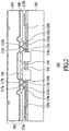
- a plurality of aluminum contacts 116 are on the top of the CMOS substrate 104 which are coupled to bond pads 105 by interconnect 107. Vias 107 are provided in both the bond pads 105 and the aluminum contacts 116 to allow for electrical connection thereto.
- the substrate 104 can comprise only a collection of metal layers and interconnects for providing for an electrical interconnection to the MEMS layers.
- the substrate 102 includes a MEMS feature 108 to complement the MEMS layers on the MEMS substrates 104, such as corresponding cavity 106.
- a gap control standoff 110 is provided to provide a precise separation of the MEMS substrate 102 from the CMOS substrate 104. The gap control standoff 110 provides a seal ring 11'2 for the device.
- Figures 3A and 3B are cross sectional and top views of a second embodiment of an assembly produced in accordance with the present invention.
- the assembly 200 includes many of the same elements as assembly 100 of Figure 2 and those elements have the same reference numerals. Additionally, the assembly 200 has via contacts 202 through the MEMS substrate 102'and the gap control standoff 110' to provide electric feedthrough of signals.
- the MEMS substrate 102 can be a silicon wafer or combination of silicon wafers assembled with all the MEMS features and functionalities including any type of preprocessed features.
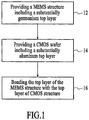
- both the CMOS wafer and the MEMS wafer are cleaned prior to bonding. Both wafers are assumed to be free of any photoresist or other extraneous materials from previous processing steps, The wafers are cleaned by: (1) a 1. 30 second dip in deionized water, (2) a 1.30 second dip in 50:1 HF; (3) a dump rinse; and (4) a standard spin-rinse-dry process.
- the bonding pair is aligned in an Electronic Visions 620 wafer-wafer aligner. Separation flags are inserted to maintain separation of the bonded pair prior to bonding.
- the aligned pair is transferred to an Electronic Visions 501 bonder.
- the purge line of this machine has been plumbed with forming gas.
- the bonding is complete and requires no further processing.
- An example of an exemplary bonding temperature profile for achieving the proper Al/Ge bond is shown in Figure 4 .
- Alternative embodiments include, for example, (1) the utilization of different materials on top of the germanium to protect it during subsequent MEMS processing; (2) the employment of different pre-bond cleaning methods; (3) the bond may be performed unaligned; (4) the bond may be performed without patterning the aluminum and/or the germanium; (5) the CMOS wafer may be bonded without any additional processing other than the pre-bond clean; (6) the aluminum-germanium bond may be configured so as not to create a hermetic seal; (7) utilization of a substrate other than a MEMS wafer (such as a simple cover wafer); (8) the MEMS substrate may comprise something other than a gyroscope (such as a pressure sensor or accelerometer); (9) the aluminum of the standard CMOS wafer may comprise different formulations of standard aluminum (2% silicon, 2% silicon/1% copper, etc.)
- a specific temperature profile can be utilized; (11) a forming gas can be used to deoxidize the contact surfaces; (12) aluminum can be utilized as the standard metalization used for IC fabrication; (13) aluminum substrate can be kept below a predetermined temperature to prevent complete leaching of aluminum and germanium alloy from the oxide on the substrate; (14) the bonding can be performed using controlled ambient such as forming gas; (15) the bonding can be performed using low pressure bonding force or high pressure bonding force as assistance for/in order to assist in breaking of the aluminum oxide to initiate the interaction; (16) two wafers can be pre-aligned prior to bonding process; (17) a special cleaning solution can be utilized to clean the oxide from both surfaces; (18) the bonding surfaces can be cleaned by sputter etching; (19) a thin layer of TiW can be utilized to protect the bonding surface during MEMS processing; (20) including pre bond cleaning using plasma and/or other insitu cleaning techniques, in addition to a more concentrated forming gas and higher force bond; (21) The germanium can be
- the germanium can be deposited on a semiconductor substrate that has been doped such that the resulting contact between the aluminum of the substrate and the MEMS is rectifying,
- This substrate can be a silicon substrate with n-type doping to 0.02-0.05 ⁇ -cm.
- the germanium can be deposited on a semiconductor substrate that has been doped such that the resulting contact between the aluminum of the substrate and the MEMS is ohmic.
- An aluminum-germanium bond has the following unique combination of attributes: (1) it can form a hermetic seal; (2) it can be used to create an electrically conductive path between two substrates; (3) it can be patterned so that this conduction path is localized; (4) the bond can be made with the aluminum that is available as a standard foundry CMOS process. This has the significant advantage of allowing for wafer-level bonding or packaging without the addition of any additional process layers to the CMOS wafer.
Landscapes
- Engineering & Computer Science (AREA)
- Microelectronics & Electronic Packaging (AREA)
- Manufacturing & Machinery (AREA)
- Computer Hardware Design (AREA)
- Chemical & Material Sciences (AREA)
- Analytical Chemistry (AREA)
- Mechanical Engineering (AREA)
- Micromachines (AREA)
- Internal Circuitry In Semiconductor Integrated Circuit Devices (AREA)
Claims (8)
- Verfahren zum Verbonden eines ersten Substrat-Wafers (104, 104') und eines zweiten Substrat-Wafers (102, 102') durch Erstellen einer Aluminium-/Germanium-Verbondung (110, 110'), wobei der erste Substrat-Wafer (104, 104') ein CMOS-Substrat-Wafer mit einer Aluminiumdeckschicht ist und sich eine Germaniumschicht auf dem zweiten Substrat-Wafer (102, 102') befindet, wobei das Verfahren folgende Schritte umfasst:Platzieren des ersten Substrat-Wafers (104, 104') in einer ersten Einspannung;Platzieren des zweiten Substrat-Wafers (102, 102') in einer zweiten Einspannung;Ausrichten des ersten Substrat-Wafers und des zweiten Substrat-Wafers; undBilden einer eutektischen Verbondung (110, 110') zwischen der Germaniumschicht und der Aluminiumdeckschicht, wobei die eutektische Verbondung durch Aufbringen einer Kraft über die erste Einspannung und die zweite Einspannung gebildet wird, und Ansteigen der Temperatur des ersten Substrat-Wafers und des zweiten Substrat-Wafers über eine eutektische Temperatur der Aluminium-/Germanium-Verbindung, wobei die auf dem ersten Substrat-Wafer befindliche Aluminiumdeckschicht eine auf dem CMOS-Substrat-Wafer befindliche Aluminiumschicht ist.
- Verfahren nach Anspruch 1, wobei das Platzieren des zweiten Substrat-Wafers (102, 102') in der zweiten Einspannung das Platzieren des eine Struktur mit einem mikro-elektro-mechanischen System (MEMS) aufweisenden zweiten Substrat-Wafers in der zweiten Einspannung umfasst.
- Verfahren nach Anspruch 2, wobei das Platzieren des ersten Substrat-Wafers (104, 104') in der ersten Einspannung das Platzieren des eine CMOS-Struktur aufweisenden ersten Substrat-Wafers in der ersten Einspannung umfasst.
- Verfahren nach Anspruch 3, wobei das Bilden der eutektischen Verbindung (110, 110') Folgendes umfasst:
Bilden, mit der Aluminium-/Germanium-Verbondung, zumindest einer elektrischen Verbindung und/oder einer hermetischen Abdichtung zwischen dem ersten Substrat-Wafer (104, 104') und dem zweiten Substrat-Wafer (102, 102'), wobei die hermetische Abdichtung eine Teilumfassung der MEMS-Struktur bildet. - Verfahren nach Anspruch 1, wobei das Bilden der eutektischen Verbondung (110, 110') Folgendes umfasst:
Bilden, mit der Aluminium-/Germanium-Verbondung, zumindest einer elektrischen Verbindung und/oder einer hermetischen Abdichtung zwischen dem ersten Substrat-Wafer (104, 104') und dem zweiten Substrat-Wafer (102, 102'). - Verfahren nach Anspruch 1, wobei die Aluminiumschicht eine strukturierte Aluminiumschicht ist und die Germaniumschicht eine strukturierte Germaniumschicht ist.
- Verfahren nach Anspruch 6, wobei das Bilden der eutektischen Verbondung (110, 110') Folgendes umfasst:
Bilden einer elektrischen Verbindung zwischen dem CMOS-Subtrat und dem zweiten Substrat-Wafer (102, 102'). - Verfahren nach Anspruch 6, das ferner Folgendes umfasst:
Bereitstellen einer Isolierschicht zwischen dem zweiten Substrat-Wafer (102, 102') und einem Abschnitt der strukturierten Germaniumschicht.
Applications Claiming Priority (4)
| Application Number | Priority Date | Filing Date | Title |
|---|---|---|---|
| US11/084,296 US7442570B2 (en) | 2005-03-18 | 2005-03-18 | Method of fabrication of a AL/GE bonding in a wafer packaging environment and a product produced therefrom |
| PCT/US2006/008543 WO2006101769A2 (en) | 2005-03-18 | 2006-03-09 | Method of fabrication of ai/ge bonding in a wafer packaging environment and a product produced therefrom |
| EP15161041.7A EP2910522B1 (de) | 2005-03-18 | 2006-03-09 | Verfahren zur herstellung von al/ge-verbindung in einem waferhäusungszusammenhang und ein daraus hergestelltes produkt |
| EP06737697.0A EP1859475B8 (de) | 2005-03-18 | 2006-03-09 | Verfahren zur herstellung von al/ge-bindung in einer waferverkapselungsumgebung und daraus hergestelltes produkt |
Related Parent Applications (3)
| Application Number | Title | Priority Date | Filing Date |
|---|---|---|---|
| EP06737697.0A Division EP1859475B8 (de) | 2005-03-18 | 2006-03-09 | Verfahren zur herstellung von al/ge-bindung in einer waferverkapselungsumgebung und daraus hergestelltes produkt |
| EP15161041.7A Division-Into EP2910522B1 (de) | 2005-03-18 | 2006-03-09 | Verfahren zur herstellung von al/ge-verbindung in einem waferhäusungszusammenhang und ein daraus hergestelltes produkt |
| EP15161041.7A Division EP2910522B1 (de) | 2005-03-18 | 2006-03-09 | Verfahren zur herstellung von al/ge-verbindung in einem waferhäusungszusammenhang und ein daraus hergestelltes produkt |
Publications (2)
| Publication Number | Publication Date |
|---|---|
| EP3208231A1 EP3208231A1 (de) | 2017-08-23 |
| EP3208231B1 true EP3208231B1 (de) | 2020-12-23 |
Family
ID=37009423
Family Applications (3)
| Application Number | Title | Priority Date | Filing Date |
|---|---|---|---|
| EP17161696.4A Expired - Lifetime EP3208231B1 (de) | 2005-03-18 | 2006-03-09 | Verfahren zur herstellung einer al/ge-verbindung im bereich der waferverkapselung |
| EP06737697.0A Expired - Lifetime EP1859475B8 (de) | 2005-03-18 | 2006-03-09 | Verfahren zur herstellung von al/ge-bindung in einer waferverkapselungsumgebung und daraus hergestelltes produkt |
| EP15161041.7A Expired - Lifetime EP2910522B1 (de) | 2005-03-18 | 2006-03-09 | Verfahren zur herstellung von al/ge-verbindung in einem waferhäusungszusammenhang und ein daraus hergestelltes produkt |
Family Applications After (2)
| Application Number | Title | Priority Date | Filing Date |
|---|---|---|---|
| EP06737697.0A Expired - Lifetime EP1859475B8 (de) | 2005-03-18 | 2006-03-09 | Verfahren zur herstellung von al/ge-bindung in einer waferverkapselungsumgebung und daraus hergestelltes produkt |
| EP15161041.7A Expired - Lifetime EP2910522B1 (de) | 2005-03-18 | 2006-03-09 | Verfahren zur herstellung von al/ge-verbindung in einem waferhäusungszusammenhang und ein daraus hergestelltes produkt |
Country Status (5)
| Country | Link |
|---|---|
| US (7) | US7442570B2 (de) |
| EP (3) | EP3208231B1 (de) |
| KR (1) | KR100934291B1 (de) |
| CN (3) | CN105206537A (de) |
| WO (1) | WO2006101769A2 (de) |
Families Citing this family (278)
| Publication number | Priority date | Publication date | Assignee | Title |
|---|---|---|---|---|
| US20060182993A1 (en) * | 2004-08-10 | 2006-08-17 | Mitsubishi Chemical Corporation | Compositions for organic electroluminescent device and organic electroluminescent device |
| US7786592B2 (en) | 2005-06-14 | 2010-08-31 | John Trezza | Chip capacitive coupling |
| US7946331B2 (en) | 2005-06-14 | 2011-05-24 | Cufer Asset Ltd. L.L.C. | Pin-type chip tooling |
| US7560813B2 (en) * | 2005-06-14 | 2009-07-14 | John Trezza | Chip-based thermo-stack |
| US7687400B2 (en) | 2005-06-14 | 2010-03-30 | John Trezza | Side stacking apparatus and method |
| US8456015B2 (en) | 2005-06-14 | 2013-06-04 | Cufer Asset Ltd. L.L.C. | Triaxial through-chip connection |
| US7838997B2 (en) | 2005-06-14 | 2010-11-23 | John Trezza | Remote chip attachment |
| US7781886B2 (en) | 2005-06-14 | 2010-08-24 | John Trezza | Electronic chip contact structure |
| US7851348B2 (en) | 2005-06-14 | 2010-12-14 | Abhay Misra | Routingless chip architecture |
| US7767493B2 (en) | 2005-06-14 | 2010-08-03 | John Trezza | Post & penetration interconnection |
| US7243833B2 (en) * | 2005-06-30 | 2007-07-17 | Intel Corporation | Electrically-isolated interconnects and seal rings in packages using a solder preform |
| US7569926B2 (en) * | 2005-08-26 | 2009-08-04 | Innovative Micro Technology | Wafer level hermetic bond using metal alloy with raised feature |
| US7541209B2 (en) * | 2005-10-14 | 2009-06-02 | Hewlett-Packard Development Company, L.P. | Method of forming a device package having edge interconnect pad |
| US20070170528A1 (en) * | 2006-01-20 | 2007-07-26 | Aaron Partridge | Wafer encapsulated microelectromechanical structure and method of manufacturing same |
| US7723811B2 (en) * | 2006-05-03 | 2010-05-25 | Hewlett-Packard Development Company, L.P. | Packaged MEMS device assembly |
| US7687397B2 (en) | 2006-06-06 | 2010-03-30 | John Trezza | Front-end processed wafer having through-chip connections |
| KR100846569B1 (ko) * | 2006-06-14 | 2008-07-15 | 매그나칩 반도체 유한회사 | Mems 소자의 패키지 및 그 제조방법 |
| KR100772321B1 (ko) * | 2006-06-14 | 2007-10-31 | 매그나칩 반도체 유한회사 | Mems 소자의 패키지 및 그 제조방법 |
| US7851876B2 (en) * | 2006-10-20 | 2010-12-14 | Hewlett-Packard Development Company, L.P. | Micro electro mechanical system |
| US20080128901A1 (en) * | 2006-11-30 | 2008-06-05 | Peter Zurcher | Micro-electro-mechanical systems device and integrated circuit device integrated in a three-dimensional semiconductor structure |
| KR100833508B1 (ko) * | 2006-12-07 | 2008-05-29 | 한국전자통신연구원 | 멤즈 패키지 및 그 방법 |
| US8508039B1 (en) | 2008-05-08 | 2013-08-13 | Invensense, Inc. | Wafer scale chip scale packaging of vertically integrated MEMS sensors with electronics |
| US8952832B2 (en) | 2008-01-18 | 2015-02-10 | Invensense, Inc. | Interfacing application programs and motion sensors of a device |
| US7934423B2 (en) | 2007-12-10 | 2011-05-03 | Invensense, Inc. | Vertically integrated 3-axis MEMS angular accelerometer with integrated electronics |
| US8047075B2 (en) | 2007-06-21 | 2011-11-01 | Invensense, Inc. | Vertically integrated 3-axis MEMS accelerometer with electronics |
| US8250921B2 (en) | 2007-07-06 | 2012-08-28 | Invensense, Inc. | Integrated motion processing unit (MPU) with MEMS inertial sensing and embedded digital electronics |
| US8020441B2 (en) | 2008-02-05 | 2011-09-20 | Invensense, Inc. | Dual mode sensing for vibratory gyroscope |
| US8141424B2 (en) | 2008-09-12 | 2012-03-27 | Invensense, Inc. | Low inertia frame for detecting coriolis acceleration |
| US8462109B2 (en) | 2007-01-05 | 2013-06-11 | Invensense, Inc. | Controlling and accessing content using motion processing on mobile devices |
| US20090265671A1 (en) * | 2008-04-21 | 2009-10-22 | Invensense | Mobile devices with motion gesture recognition |
| US7796872B2 (en) | 2007-01-05 | 2010-09-14 | Invensense, Inc. | Method and apparatus for producing a sharp image from a handheld device containing a gyroscope |
| US7670874B2 (en) * | 2007-02-16 | 2010-03-02 | John Trezza | Plated pillar package formation |
| EP1977991A3 (de) * | 2007-04-05 | 2013-08-14 | Fraunhofer-Gesellschaft zur Förderung der angewandten Forschung e.V. | Mikrostrukturierte Bauteile mit einem Substrat und einem an das Substrat direkt ankontaktierten Chip, sowie Verfahren zu deren Herstellung |
| DE102007044806A1 (de) * | 2007-09-20 | 2009-04-02 | Robert Bosch Gmbh | Mikromechanisches Bauelement und Verfahren zur Herstellung eines mikromechanischen Bauelements |
| DE102007048604A1 (de) | 2007-10-10 | 2009-04-16 | Robert Bosch Gmbh | Verbund aus mindestens zwei Halbleitersubstraten sowie Herstellungsverfahren |
| KR101301157B1 (ko) * | 2007-11-09 | 2013-09-03 | 삼성전자주식회사 | 다단계 기판 식각 방법 및 이를 이용하여 제조된테라헤르츠 발진기 |
| DE102007054505B4 (de) | 2007-11-15 | 2016-12-22 | Robert Bosch Gmbh | Drehratensensor |
| EP2244968A2 (de) * | 2008-01-21 | 2010-11-03 | Nxp B.V. | Saubere und luftdichte versiegelung einer verpackungsvertiefung |
| US8766512B2 (en) * | 2009-03-31 | 2014-07-01 | Sand 9, Inc. | Integration of piezoelectric materials with substrates |
| US8044737B2 (en) * | 2008-04-29 | 2011-10-25 | Sand9, Inc. | Timing oscillators and related methods |
| US8410868B2 (en) | 2009-06-04 | 2013-04-02 | Sand 9, Inc. | Methods and apparatus for temperature control of devices and mechanical resonating structures |
| US8476809B2 (en) | 2008-04-29 | 2013-07-02 | Sand 9, Inc. | Microelectromechanical systems (MEMS) resonators and related apparatus and methods |
| US8044736B2 (en) * | 2008-04-29 | 2011-10-25 | Sand9, Inc. | Timing oscillators and related methods |
| US20090289349A1 (en) * | 2008-05-21 | 2009-11-26 | Spatial Photonics, Inc. | Hermetic sealing of micro devices |
| DE102008041674A1 (de) * | 2008-08-28 | 2010-03-04 | Robert Bosch Gmbh | Mikromechanisches Bauelement und entsprechendes Herstellungsverfahren |
| DE102008041750A1 (de) * | 2008-09-02 | 2010-03-18 | Robert Bosch Gmbh | Thermisch entkoppeltes mikrostrukturiertes Referenzelement für Sensoren |
| US7943411B2 (en) * | 2008-09-10 | 2011-05-17 | Analog Devices, Inc. | Apparatus and method of wafer bonding using compatible alloy |
| US8956904B2 (en) | 2008-09-10 | 2015-02-17 | Analog Devices, Inc. | Apparatus and method of wafer bonding using compatible alloy |
| JP5314979B2 (ja) * | 2008-09-22 | 2013-10-16 | アルプス電気株式会社 | Memsセンサ |
| JP5222947B2 (ja) * | 2008-09-22 | 2013-06-26 | アルプス電気株式会社 | Memsセンサ |
| US8207586B2 (en) * | 2008-09-22 | 2012-06-26 | Alps Electric Co., Ltd. | Substrate bonded MEMS sensor |
| DE102008042382A1 (de) * | 2008-09-26 | 2010-04-01 | Robert Bosch Gmbh | Kontaktanordnung zur Herstellung einer beabstandeten, elektrisch leitfähigen Verbindung zwischen mikrostrukturierten Bauteilen |
| US8089144B2 (en) | 2008-12-17 | 2012-01-03 | Denso Corporation | Semiconductor device and method for manufacturing the same |
| JP4883077B2 (ja) * | 2008-12-17 | 2012-02-22 | 株式会社デンソー | 半導体装置およびその製造方法 |
| US8058143B2 (en) * | 2009-01-21 | 2011-11-15 | Freescale Semiconductor, Inc. | Substrate bonding with metal germanium silicon material |
| US8928602B1 (en) | 2009-03-03 | 2015-01-06 | MCube Inc. | Methods and apparatus for object tracking on a hand-held device |
| US8797279B2 (en) | 2010-05-25 | 2014-08-05 | MCube Inc. | Analog touchscreen methods and apparatus |
| US9048811B2 (en) | 2009-03-31 | 2015-06-02 | Sand 9, Inc. | Integration of piezoelectric materials with substrates |
| DE102009002363B4 (de) * | 2009-04-14 | 2019-03-07 | Robert Bosch Gmbh | Verfahren zum Befestigen einer ersten Trägereinrichtung an einer zweiten Trägereinrichtung |
| CN101870444B (zh) * | 2009-04-22 | 2014-08-13 | 原相科技股份有限公司 | 具有功能连结导线的微机电系统芯片 |
| SE537499C2 (sv) | 2009-04-30 | 2015-05-26 | Silex Microsystems Ab | Bondningsmaterialstruktur och process med bondningsmaterialstruktur |
| US20100283138A1 (en) * | 2009-05-06 | 2010-11-11 | Analog Devices, Inc. | Nickel-Based Bonding of Semiconductor Wafers |
| US8421082B1 (en) | 2010-01-19 | 2013-04-16 | Mcube, Inc. | Integrated CMOS and MEMS with air dielectric method and system |
| US8823007B2 (en) | 2009-10-28 | 2014-09-02 | MCube Inc. | Integrated system on chip using multiple MEMS and CMOS devices |
| US8553389B1 (en) | 2010-08-19 | 2013-10-08 | MCube Inc. | Anchor design and method for MEMS transducer apparatuses |
| US8477473B1 (en) | 2010-08-19 | 2013-07-02 | MCube Inc. | Transducer structure and method for MEMS devices |
| US8710597B1 (en) * | 2010-04-21 | 2014-04-29 | MCube Inc. | Method and structure for adding mass with stress isolation to MEMS structures |
| US8476129B1 (en) | 2010-05-24 | 2013-07-02 | MCube Inc. | Method and structure of sensors and MEMS devices using vertical mounting with interconnections |
| SG179006A1 (en) | 2009-09-25 | 2012-04-27 | Agency Science Tech & Res | A wafer level package and a method of forming a wafer level package |
| US9709509B1 (en) | 2009-11-13 | 2017-07-18 | MCube Inc. | System configured for integrated communication, MEMS, Processor, and applications using a foundry compatible semiconductor process |
| US8119431B2 (en) * | 2009-12-08 | 2012-02-21 | Freescale Semiconductor, Inc. | Method of forming a micro-electromechanical system (MEMS) having a gap stop |
| JP5367841B2 (ja) * | 2009-12-11 | 2013-12-11 | パイオニア株式会社 | 半導体基板の接合方法およびmemsデバイス |
| JP5021098B2 (ja) | 2009-12-11 | 2012-09-05 | パイオニア株式会社 | 半導体基板の接合方法およびmemsデバイス |
| US8794065B1 (en) | 2010-02-27 | 2014-08-05 | MCube Inc. | Integrated inertial sensing apparatus using MEMS and quartz configured on crystallographic planes |
| US8936959B1 (en) | 2010-02-27 | 2015-01-20 | MCube Inc. | Integrated rf MEMS, control systems and methods |
| CN102792168B (zh) * | 2010-03-09 | 2014-04-30 | 阿尔卑斯电气株式会社 | Mems传感器 |
| US8647962B2 (en) * | 2010-03-23 | 2014-02-11 | Taiwan Semiconductor Manufacturing Company, Ltd. | Wafer level packaging bond |
| US8367522B1 (en) | 2010-04-08 | 2013-02-05 | MCube Inc. | Method and structure of integrated micro electro-mechanical systems and electronic devices using edge bond pads |
| US8928696B1 (en) | 2010-05-25 | 2015-01-06 | MCube Inc. | Methods and apparatus for operating hysteresis on a hand held device |
| US8966400B2 (en) | 2010-06-07 | 2015-02-24 | Empire Technology Development Llc | User movement interpretation in computer generated reality |
| US8869616B1 (en) | 2010-06-18 | 2014-10-28 | MCube Inc. | Method and structure of an inertial sensor using tilt conversion |
| US8652961B1 (en) | 2010-06-18 | 2014-02-18 | MCube Inc. | Methods and structure for adapting MEMS structures to form electrical interconnections for integrated circuits |
| US8993362B1 (en) | 2010-07-23 | 2015-03-31 | MCube Inc. | Oxide retainer method for MEMS devices |
| US8648468B2 (en) | 2010-07-29 | 2014-02-11 | Taiwan Semiconductor Manufacturing Company, Ltd. | Hermetic wafer level packaging |
| CN103221331B (zh) * | 2010-09-18 | 2016-02-03 | 快捷半导体公司 | 用于微机电系统的密封封装 |
| EP2616771B8 (de) | 2010-09-18 | 2018-12-19 | Fairchild Semiconductor Corporation | Mikroverarbeiteter monolithischer inertialsensor mit sechs achsen |
| WO2012037501A2 (en) | 2010-09-18 | 2012-03-22 | Cenk Acar | Flexure bearing to reduce quadrature for resonating micromachined devices |
| WO2012037492A2 (en) | 2010-09-18 | 2012-03-22 | Janusz Bryzek | Multi-die mems package |
| US9278845B2 (en) | 2010-09-18 | 2016-03-08 | Fairchild Semiconductor Corporation | MEMS multi-axis gyroscope Z-axis electrode structure |
| US9455354B2 (en) | 2010-09-18 | 2016-09-27 | Fairchild Semiconductor Corporation | Micromachined 3-axis accelerometer with a single proof-mass |
| WO2012040211A2 (en) | 2010-09-20 | 2012-03-29 | Fairchild Semiconductor Corporation | Microelectromechanical pressure sensor including reference capacitor |
| US8810027B2 (en) * | 2010-09-27 | 2014-08-19 | Taiwan Semiconductor Manufacturing Company, Ltd. | Bond ring for a first and second substrate |
| US8507913B2 (en) | 2010-09-29 | 2013-08-13 | Analog Devices, Inc. | Method of bonding wafers |
| US8674495B2 (en) | 2010-10-08 | 2014-03-18 | Taiwan Semiconductor Manufacturing Company, Ltd. | Package systems having a eutectic bonding material and manufacturing methods thereof |
| US9000578B2 (en) * | 2010-10-08 | 2015-04-07 | Taiwan Semiconductor Manufacturing Company, Ltd. | Package systems having an opening in a substrate thereof and manufacturing methods thereof |
| US8723986B1 (en) * | 2010-11-04 | 2014-05-13 | MCube Inc. | Methods and apparatus for initiating image capture on a hand-held device |
| US9276080B2 (en) | 2012-03-09 | 2016-03-01 | Mcube, Inc. | Methods and structures of integrated MEMS-CMOS devices |
| US20120235251A1 (en) * | 2011-03-14 | 2012-09-20 | Invensense, Inc. | Wafer level packaging of mems devices |
| CN102156012A (zh) * | 2011-03-15 | 2011-08-17 | 迈尔森电子(天津)有限公司 | Mems压力传感器及其制作方法 |
| US8378490B2 (en) * | 2011-03-15 | 2013-02-19 | Taiwan Semiconductor Manufacturing Company, Ltd. | Semiconductor apparatus including a metal alloy between a first contact and a second contact |
| US9278853B2 (en) | 2011-03-28 | 2016-03-08 | Miramems Sensing Technology Co., Ltd. | Manufacturing process of MEMS device |
| US8754529B2 (en) * | 2011-03-28 | 2014-06-17 | Miradia, Inc. | MEMS device with simplified electrical conducting paths |
| US8741738B2 (en) * | 2011-06-08 | 2014-06-03 | Taiwan Semiconductor Manufacturing Company, Ltd. | Method of fabrication of a semiconductor apparatus comprising substrates including Al/Ge and Cu contact layers to form a metallic alloy |
| DE102011077933B4 (de) | 2011-06-21 | 2014-07-10 | Robert Bosch Gmbh | Verfahren zum Bonden zweier Substrate |
| US9452925B2 (en) | 2011-06-27 | 2016-09-27 | Invensense, Inc. | Method of increasing MEMS enclosure pressure using outgassing material |
| US9540230B2 (en) | 2011-06-27 | 2017-01-10 | Invensense, Inc. | Methods for CMOS-MEMS integrated devices with multiple sealed cavities maintained at various pressures |
| US9718679B2 (en) | 2011-06-27 | 2017-08-01 | Invensense, Inc. | Integrated heater for gettering or outgassing activation |
| KR101646999B1 (ko) * | 2011-06-29 | 2016-08-09 | 인벤센스, 인크. | 수직으로 집적된 전자장치를 갖는 환경에 노출된 부분을 구비한 기밀하게 밀봉된 mems 디바이스 |
| FR2977884B1 (fr) | 2011-07-12 | 2016-01-29 | Commissariat Energie Atomique | Procede de realisation d'une structure a membrane suspendue et a electrode enterree |
| FR2977885A1 (fr) | 2011-07-12 | 2013-01-18 | Commissariat Energie Atomique | Procede de realisation d'une structure a electrode enterree par report direct et structure ainsi obtenue |
| US8969101B1 (en) | 2011-08-17 | 2015-03-03 | MCube Inc. | Three axis magnetic sensor device and method using flex cables |
| JP6034619B2 (ja) * | 2011-08-22 | 2016-11-30 | パナソニック株式会社 | Mems素子およびそれを用いた電気機器 |
| DE102011089569B4 (de) * | 2011-12-22 | 2024-08-22 | Robert Bosch Gmbh | Verfahren zum Verbinden zweier Siliziumsubstrate und entsprechende Anordnung zweier Siliziumsubstrate |
| CN103183308B (zh) * | 2011-12-30 | 2016-08-03 | 中芯国际集成电路制造(上海)有限公司 | Al-Ge键合方法 |
| US9139423B2 (en) * | 2012-01-19 | 2015-09-22 | Taiwan Semiconductor Manufacturing Company, Ltd. | Micro electro mechanical system structures |
| US9062972B2 (en) | 2012-01-31 | 2015-06-23 | Fairchild Semiconductor Corporation | MEMS multi-axis accelerometer electrode structure |
| US8716852B2 (en) * | 2012-02-17 | 2014-05-06 | Taiwan Semiconductor Manufacturing Company, Ltd. | Micro-electro mechanical systems (MEMS) having outgasing prevention structures and methods of forming the same |
| CN107671412A (zh) * | 2012-03-19 | 2018-02-09 | Ev 集团 E·索尔纳有限责任公司 | 用于对接合压力进行压力传递的压力传递板 |
| US9488693B2 (en) | 2012-04-04 | 2016-11-08 | Fairchild Semiconductor Corporation | Self test of MEMS accelerometer with ASICS integrated capacitors |
| EP2647952B1 (de) | 2012-04-05 | 2017-11-15 | Fairchild Semiconductor Corporation | Automatische Verstärkungsregelungsschleife einer MEMS-Vorrichtung für mechanischen Amplitudenantrieb |
| EP2647955B8 (de) | 2012-04-05 | 2018-12-19 | Fairchild Semiconductor Corporation | MEMS-Vorrichtung mit Quadraturphasenverschiebungsauslöschung |
| KR102058489B1 (ko) | 2012-04-05 | 2019-12-23 | 페어차일드 세미컨덕터 코포레이션 | 멤스 장치 프론트 엔드 전하 증폭기 |
| CN102633228A (zh) * | 2012-04-09 | 2012-08-15 | 武汉高德红外股份有限公司 | 新型cmos-mems兼容的非制冷红外传感器晶圆级封装方法 |
| US9625272B2 (en) | 2012-04-12 | 2017-04-18 | Fairchild Semiconductor Corporation | MEMS quadrature cancellation and signal demodulation |
| US9738512B2 (en) | 2012-06-27 | 2017-08-22 | Invensense, Inc. | CMOS-MEMS integrated device including multiple cavities at different controlled pressures and methods of manufacture |
| US9040355B2 (en) * | 2012-07-11 | 2015-05-26 | Freescale Semiconductor, Inc. | Sensor package and method of forming same |
| US8940616B2 (en) | 2012-07-27 | 2015-01-27 | Globalfoundries Singapore Pte. Ltd. | Bonding method using porosified surfaces for making stacked structures |
| DE102013014881B4 (de) | 2012-09-12 | 2023-05-04 | Fairchild Semiconductor Corporation | Verbesserte Silizium-Durchkontaktierung mit einer Füllung aus mehreren Materialien |
| US8736045B1 (en) * | 2012-11-02 | 2014-05-27 | Raytheon Company | Integrated bondline spacers for wafer level packaged circuit devices |
| US10160638B2 (en) | 2013-01-04 | 2018-12-25 | Taiwan Semiconductor Manufacturing Company, Ltd. | Method and apparatus for a semiconductor structure |
| US9006015B2 (en) | 2013-01-24 | 2015-04-14 | Taiwan Semiconductor Manfacturing Company, Ltd. | Dual layer microelectromechanical systems device and method of manufacturing same |
| TWI512938B (zh) | 2013-01-28 | 2015-12-11 | Asia Pacific Microsystems Inc | 整合式微機電元件及其製造方法 |
| US8564076B1 (en) | 2013-01-30 | 2013-10-22 | Invensense, Inc. | Internal electrical contact for enclosed MEMS devices |
| CN103964375B (zh) * | 2013-02-01 | 2018-10-16 | 中芯国际集成电路制造(上海)有限公司 | 芯片键合方法 |
| US9533873B2 (en) | 2013-02-05 | 2017-01-03 | Butterfly Network, Inc. | CMOS ultrasonic transducers and related apparatus and methods |
| CN104051385B (zh) * | 2013-03-13 | 2017-06-13 | 台湾积体电路制造股份有限公司 | 堆叠式半导体结构及其形成方法 |
| CN104045051B (zh) * | 2013-03-13 | 2016-08-17 | 台湾积体电路制造股份有限公司 | 堆叠半导体器件及其形成方法 |
| US9975762B2 (en) | 2013-03-13 | 2018-05-22 | Taiwan Semiconductor Manufacturing Company, Ltd. | Stacked semiconductor structure and method of forming the same |
| US20140264655A1 (en) * | 2013-03-13 | 2014-09-18 | Invensense, Inc. | Surface roughening to reduce adhesion in an integrated mems device |
| US9035428B2 (en) | 2013-03-14 | 2015-05-19 | Invensense, Inc. | Integrated structure with bidirectional vertical actuation |
| WO2014151525A2 (en) | 2013-03-15 | 2014-09-25 | Butterfly Network, Inc. | Complementary metal oxide semiconductor (cmos) ultrasonic transducers and methods for forming the same |
| CN104241147A (zh) * | 2013-06-14 | 2014-12-24 | 无锡华润上华半导体有限公司 | 一种基于铝锗共晶的低温键合方法 |
| US10273147B2 (en) | 2013-07-08 | 2019-04-30 | Motion Engine Inc. | MEMS components and method of wafer-level manufacturing thereof |
| JP6339669B2 (ja) | 2013-07-08 | 2018-06-06 | モーション・エンジン・インコーポレーテッド | Memsデバイスおよび製造する方法 |
| NO2944700T3 (de) * | 2013-07-11 | 2018-03-17 | ||
| US9911563B2 (en) * | 2013-07-31 | 2018-03-06 | Analog Devices Global | MEMS switch device and method of fabrication |
| WO2015013827A1 (en) | 2013-08-02 | 2015-02-05 | Motion Engine Inc. | Mems motion sensor for sub-resonance angular rate sensing |
| TW201508890A (zh) * | 2013-08-21 | 2015-03-01 | Richtek Technology Corp | 微機電系統元件製造方法及以此方法製造之微機電系統元件 |
| US9254997B2 (en) * | 2013-08-29 | 2016-02-09 | Taiwan Semiconductor Manufacturing Co., Ltd. | CMOS-MEMS integrated flow for making a pressure sensitive transducer |
| US9738511B2 (en) | 2013-09-13 | 2017-08-22 | Invensense, Inc. | Reduction of chipping damage to MEMS structure |
| CN103523745B (zh) * | 2013-10-21 | 2015-10-28 | 安徽北方芯动联科微系统技术有限公司 | 基于Si导电柱的圆片级封装方法及其单片集成式MEMS芯片 |
| US9269679B2 (en) * | 2013-11-05 | 2016-02-23 | Taiwan Semiconductor Manufacturing Co., Ltd. | Wafer level packaging techniques |
| DE102013222616B4 (de) | 2013-11-07 | 2024-06-06 | Robert Bosch Gmbh | Mikromechanische Sensorvorrichtung |
| WO2015103688A1 (en) | 2014-01-09 | 2015-07-16 | Motion Engine Inc. | Integrated mems system |
| DE102014200512B4 (de) * | 2014-01-14 | 2017-06-08 | Robert Bosch Gmbh | Mikromechanische Drucksensorvorrichtung und entsprechendes Herstellungsverfahren |
| DE102014200500A1 (de) | 2014-01-14 | 2015-07-16 | Robert Bosch Gmbh | Mikromechanische Drucksensorvorrichtung und entsprechendes Herstellungsverfahren |
| DE102014200507A1 (de) | 2014-01-14 | 2015-07-16 | Robert Bosch Gmbh | Mikromechanische Drucksensorvorrichtung und entsprechendes Herstellungsverfahren |
| DE102014202808A1 (de) | 2014-02-17 | 2015-08-20 | Robert Bosch Gmbh | Verfahren zum eutektischen Bonden zweier Trägereinrichtungen |
| GB2524235A (en) | 2014-03-07 | 2015-09-23 | Melexis Technologies Nv | Semiconductor device having a transparent window for passing radiation |
| US20150262902A1 (en) | 2014-03-12 | 2015-09-17 | Invensas Corporation | Integrated circuits protected by substrates with cavities, and methods of manufacture |
| JP6331535B2 (ja) * | 2014-03-18 | 2018-05-30 | セイコーエプソン株式会社 | 電子デバイス、電子機器および移動体 |
| EP3127158B1 (de) * | 2014-04-04 | 2019-06-12 | Robert Bosch GmbH | Membranbasierter sensor und verfahren zur robusten herstellung eines membranbasierten sensors |
| US20170030788A1 (en) | 2014-04-10 | 2017-02-02 | Motion Engine Inc. | Mems pressure sensor |
| CA2946133A1 (en) | 2014-04-18 | 2015-10-22 | Butterfly Network, Inc. | Ultrasonic transducers in complementary metal oxide semiconductor (cmos) wafers and related apparatus and methods |
| CN105084294A (zh) * | 2014-04-21 | 2015-11-25 | 中芯国际集成电路制造(上海)有限公司 | 一种mems器件及其制备方法、电子装置 |
| US9761557B2 (en) * | 2014-04-28 | 2017-09-12 | Invensense, Inc. | CMOS-MEMS integration by sequential bonding method |
| CN103979481B (zh) * | 2014-05-28 | 2016-04-20 | 杭州士兰集成电路有限公司 | Mems铝锗键合结构及其制造方法 |
| CN105225923B (zh) * | 2014-05-29 | 2019-11-26 | 上海矽睿科技有限公司 | 用于键合的铝材料的预处理方法及键合方法 |
| US11674803B2 (en) | 2014-06-02 | 2023-06-13 | Motion Engine, Inc. | Multi-mass MEMS motion sensor |
| US9513184B2 (en) * | 2014-06-11 | 2016-12-06 | Ams International Ag | MEMS device calibration |
| DE102014211558A1 (de) * | 2014-06-17 | 2015-12-17 | Robert Bosch Gmbh | Mikroelektromechanisches System und Verfahren zum Herstellen eines mikroelektromechanischen Systems |
| DE102014212314B4 (de) | 2014-06-26 | 2025-08-07 | Robert Bosch Gmbh | Mikromechanische Sensoreinrichtung |
| US9463976B2 (en) | 2014-06-27 | 2016-10-11 | Freescale Semiconductor, Inc. | MEMS fabrication process with two cavities operating at different pressures |
| US9418830B2 (en) | 2014-06-27 | 2016-08-16 | Freescale Semiconductor, Inc. | Methods for bonding semiconductor wafers |
| US9067779B1 (en) | 2014-07-14 | 2015-06-30 | Butterfly Network, Inc. | Microfabricated ultrasonic transducers and related apparatus and methods |
| JP2016048176A (ja) * | 2014-08-27 | 2016-04-07 | セイコーエプソン株式会社 | 物理量センサー、電子機器および移動体 |
| US9611133B2 (en) * | 2014-09-11 | 2017-04-04 | Invensense, Inc. | Film induced interface roughening and method of producing the same |
| DE102014221618A1 (de) | 2014-10-24 | 2016-04-28 | Robert Bosch Gmbh | Verfahren zum Verbinden zweier Substrate, entsprechende Anordnung zweier Substrate und entsprechendes Substrat |
| WO2016080506A1 (ja) | 2014-11-21 | 2016-05-26 | 株式会社村田製作所 | ウエハの接合方法 |
| DE102014224559B4 (de) | 2014-12-01 | 2025-12-31 | Robert Bosch Gmbh | Mikromechanische Sensorvorrichtung und entsprechendes Herstellungsverfahren |
| US11287486B2 (en) | 2014-12-09 | 2022-03-29 | Motion Engine, Inc. | 3D MEMS magnetometer and associated methods |
| DE102014226436A1 (de) | 2014-12-18 | 2016-06-23 | Robert Bosch Gmbh | Mikromechanische Sensorvorrichtung und entsprechendes Herstellungsverfahren |
| JP6279464B2 (ja) | 2014-12-26 | 2018-02-14 | 株式会社東芝 | センサおよびその製造方法 |
| US10407299B2 (en) | 2015-01-15 | 2019-09-10 | Motion Engine Inc. | 3D MEMS device with hermetic cavity |
| CN105990165B (zh) * | 2015-02-02 | 2019-01-22 | 中芯国际集成电路制造(上海)有限公司 | 半导体结构及其形成方法 |
| CN105984835B (zh) * | 2015-02-16 | 2017-11-10 | 中芯国际集成电路制造(上海)有限公司 | 一种mems器件及其制作方法和电子装置 |
| TWI676590B (zh) | 2015-03-17 | 2019-11-11 | 美商伊凡聖斯股份有限公司 | 具有雙腔壓力結構之半導體裝置及其製造方法 |
| US9682854B2 (en) | 2015-04-10 | 2017-06-20 | Memsic, Inc | Wafer level chip scale packaged micro-electro-mechanical-system (MEMS) device and methods of producing thereof |
| CN104891429A (zh) * | 2015-04-17 | 2015-09-09 | 上海华虹宏力半导体制造有限公司 | 一种改善铝锗共晶键合工艺的方法 |
| CN106206624A (zh) * | 2015-04-29 | 2016-12-07 | 中国科学院微电子研究所 | 一种晶圆级封装盖帽及其制作方法 |
| CN105016291A (zh) * | 2015-06-07 | 2015-11-04 | 上海华虹宏力半导体制造有限公司 | 可减少mems键合过程中铝锗键合桥连的结构 |
| CN106373900A (zh) * | 2015-07-20 | 2017-02-01 | 中芯国际集成电路制造(北京)有限公司 | 晶圆级键合封装方法以及共晶键合的晶圆结构 |
| DE102015217921A1 (de) | 2015-09-18 | 2017-03-23 | Robert Bosch Gmbh | Mikromechanisches Bauelement |
| DE102015217928A1 (de) | 2015-09-18 | 2017-03-23 | Robert Bosch Gmbh | Mikromechanisches Bauelement |
| DE102015217918A1 (de) | 2015-09-18 | 2017-03-23 | Robert Bosch Gmbh | Mikromechanisches Bauelement |
| CN105293428B (zh) * | 2015-10-19 | 2017-04-19 | 北京航天控制仪器研究所 | 一种mems器件的全硅化圆片级真空封装方法及封装器件 |
| FR3042909B1 (fr) | 2015-10-21 | 2017-12-15 | Commissariat Energie Atomique | Procede d'encapsulation d'un composant microelectronique |
| TWI676591B (zh) | 2015-10-28 | 2019-11-11 | 美商伊凡聖斯股份有限公司 | 用於具有微機電系統(mems)間隙控制結構之mems裝置的方法及設備 |
| US9987661B2 (en) | 2015-12-02 | 2018-06-05 | Butterfly Network, Inc. | Biasing of capacitive micromachined ultrasonic transducers (CMUTs) and related apparatus and methods |
| US11078075B2 (en) | 2015-12-31 | 2021-08-03 | Taiwan Semiconductor Manufacturing Company Ltd. | Packaging method and associated packaging structure |
| CN107226453B (zh) * | 2016-03-24 | 2021-08-13 | 中芯国际集成电路制造(上海)有限公司 | 一种mems器件及其制备方法、电子装置 |
| DE102016206607B4 (de) | 2016-04-19 | 2021-09-16 | Robert Bosch Gmbh | Elektronisches Bauelement und Verfahren zum Herstellen eines elektronischen Bauelements |
| WO2017192899A1 (en) | 2016-05-04 | 2017-11-09 | Invensense, Inc. | A two-dimensional array of cmos control elements |
| US10656255B2 (en) | 2016-05-04 | 2020-05-19 | Invensense, Inc. | Piezoelectric micromachined ultrasonic transducer (PMUT) |
| US10445547B2 (en) | 2016-05-04 | 2019-10-15 | Invensense, Inc. | Device mountable packaging of ultrasonic transducers |
| US10670716B2 (en) | 2016-05-04 | 2020-06-02 | Invensense, Inc. | Operating a two-dimensional array of ultrasonic transducers |
| US10706835B2 (en) | 2016-05-10 | 2020-07-07 | Invensense, Inc. | Transmit beamforming of a two-dimensional array of ultrasonic transducers |
| US10408797B2 (en) | 2016-05-10 | 2019-09-10 | Invensense, Inc. | Sensing device with a temperature sensor |
| US10632500B2 (en) | 2016-05-10 | 2020-04-28 | Invensense, Inc. | Ultrasonic transducer with a non-uniform membrane |
| US10539539B2 (en) | 2016-05-10 | 2020-01-21 | Invensense, Inc. | Operation of an ultrasonic sensor |
| US10452887B2 (en) | 2016-05-10 | 2019-10-22 | Invensense, Inc. | Operating a fingerprint sensor comprised of ultrasonic transducers |
| US10600403B2 (en) | 2016-05-10 | 2020-03-24 | Invensense, Inc. | Transmit operation of an ultrasonic sensor |
| US10562070B2 (en) | 2016-05-10 | 2020-02-18 | Invensense, Inc. | Receive operation of an ultrasonic sensor |
| US9868630B2 (en) * | 2016-05-20 | 2018-01-16 | Taiwan Semiconductor Manufacturing Co., Ltd. | Package structure and manufacturing method thereof |
| CN106115608B (zh) * | 2016-05-31 | 2017-08-11 | 苏州希美微纳系统有限公司 | 针对射频mems器件应用的横向互连低温圆片级封装方法 |
| DE102016210007A1 (de) * | 2016-06-07 | 2017-12-07 | Robert Bosch Gmbh | Verfahren zum eutektischen Bonden von Wafern und Waferverbund |
| US9919915B2 (en) * | 2016-06-14 | 2018-03-20 | Invensense, Inc. | Method and system for MEMS devices with dual damascene formed electrodes |
| IT201600083804A1 (it) | 2016-08-09 | 2018-02-09 | St Microelectronics Srl | Procedimento di fabbricazione di un dispositivo a semiconduttore includente una struttura microelettromeccanica ed un associato circuito elettronico integrato e relativo dispositivo a semiconduttore |
| DE102016216207A1 (de) | 2016-08-29 | 2018-03-01 | Robert Bosch Gmbh | Verfahren zum Herstellen eines mikromechanischen Sensors |
| US10192850B1 (en) | 2016-09-19 | 2019-01-29 | Sitime Corporation | Bonding process with inhibited oxide formation |
| US11097942B2 (en) * | 2016-10-26 | 2021-08-24 | Analog Devices, Inc. | Through silicon via (TSV) formation in integrated circuits |
| DE102016223203A1 (de) | 2016-11-23 | 2018-05-24 | Robert Bosch Gmbh | MEMS-Bauelement mit niederohmiger Verdrahtung und Verfahren zur Herstellung desselben |
| US10002844B1 (en) | 2016-12-21 | 2018-06-19 | Invensas Bonding Technologies, Inc. | Bonded structures |
| JP7030825B2 (ja) * | 2017-02-09 | 2022-03-07 | インヴェンサス ボンディング テクノロジーズ インコーポレイテッド | 接合構造物 |
| US10005660B1 (en) * | 2017-02-15 | 2018-06-26 | Advanced Semiconductor Engineering, Inc. | Semiconductor package device including microelectromechanical system |
| US10196261B2 (en) | 2017-03-08 | 2019-02-05 | Butterfly Network, Inc. | Microfabricated ultrasonic transducers and related apparatus and methods |
| FR3063991B1 (fr) | 2017-03-16 | 2019-05-03 | Safran | Micro-dispositif a plusieurs elements mobiles disposes au sein de plusieurs cavites imbriquees |
| US10508030B2 (en) | 2017-03-21 | 2019-12-17 | Invensas Bonding Technologies, Inc. | Seal for microelectronic assembly |
| US10793427B2 (en) | 2017-04-04 | 2020-10-06 | Kionix, Inc. | Eutectic bonding with AlGe |
| US10167191B2 (en) | 2017-04-04 | 2019-01-01 | Kionix, Inc. | Method for manufacturing a micro electro-mechanical system |
| CN107055456A (zh) * | 2017-04-14 | 2017-08-18 | 上海华虹宏力半导体制造有限公司 | 微机电系统器件的封装结构及方法 |
| CN107359156B (zh) * | 2017-05-31 | 2020-03-17 | 中国电子科技集团公司第十三研究所 | 异质集成的硅基射频微系统结构及其制作方法 |
| EP3642611B1 (de) | 2017-06-21 | 2024-02-14 | Butterfly Network, Inc. | Mikrogefertigter ultraschallwandler mit einzelnen zellen mit elektrisch isolierten elektrodenabschnitten |
| US10643052B2 (en) | 2017-06-28 | 2020-05-05 | Invensense, Inc. | Image generation in an electronic device using ultrasonic transducers |
| KR101972793B1 (ko) * | 2017-07-21 | 2019-04-29 | (주)에이엠티솔루션 | 반도체 챔버 온도 측정용 웨이퍼 레벨 패키징 방식의 수동형 표면탄성파 무선 웨이퍼 |
| US10053360B1 (en) | 2017-08-11 | 2018-08-21 | Kionix, Inc. | Pseudo SOI process |
| US10498001B2 (en) | 2017-08-21 | 2019-12-03 | Texas Instruments Incorporated | Launch structures for a hermetically sealed cavity |
| US10775422B2 (en) | 2017-09-05 | 2020-09-15 | Texas Instruments Incorporated | Molecular spectroscopy cell with resonant cavity |
| US10589986B2 (en) | 2017-09-06 | 2020-03-17 | Texas Instruments Incorporated | Packaging a sealed cavity in an electronic device |
| US10444102B2 (en) | 2017-09-07 | 2019-10-15 | Texas Instruments Incorporated | Pressure measurement based on electromagnetic signal output of a cavity |
| US10424523B2 (en) | 2017-09-07 | 2019-09-24 | Texas Instruments Incorporated | Hermetically sealed molecular spectroscopy cell with buried ground plane |
| US10549986B2 (en) | 2017-09-07 | 2020-02-04 | Texas Instruments Incorporated | Hermetically sealed molecular spectroscopy cell |
| US10131115B1 (en) * | 2017-09-07 | 2018-11-20 | Texas Instruments Incorporated | Hermetically sealed molecular spectroscopy cell with dual wafer bonding |
| US10551265B2 (en) | 2017-09-07 | 2020-02-04 | Texas Instruments Incorporated | Pressure sensing using quantum molecular rotational state transitions |
| US10544039B2 (en) | 2017-09-08 | 2020-01-28 | Texas Instruments Incorporated | Methods for depositing a measured amount of a species in a sealed cavity |
| US10301171B1 (en) | 2017-11-13 | 2019-05-28 | Globalfoundries Singapore Pte. Ltd. | Wafer level packaging for MEMS device |
| US10793421B2 (en) | 2017-11-13 | 2020-10-06 | Vanguard International Semiconductor Singapore Pte. Ltd. | Wafer level encapsulation for MEMS device |
| WO2019102872A1 (ja) | 2017-11-27 | 2019-05-31 | 株式会社村田製作所 | 共振装置 |
| US10584027B2 (en) * | 2017-12-01 | 2020-03-10 | Elbit Systems Of America, Llc | Method for forming hermetic seals in MEMS devices |
| US11380597B2 (en) | 2017-12-22 | 2022-07-05 | Invensas Bonding Technologies, Inc. | Bonded structures |
| US10923408B2 (en) | 2017-12-22 | 2021-02-16 | Invensas Bonding Technologies, Inc. | Cavity packages |
| FI20185058A1 (en) * | 2018-01-22 | 2019-07-23 | Tikitin Oy | Packaged microelectronic component and method for its manufacture |
| US10755067B2 (en) | 2018-03-22 | 2020-08-25 | Invensense, Inc. | Operating a fingerprint sensor comprised of ultrasonic transducers |
| US11004757B2 (en) | 2018-05-14 | 2021-05-11 | Invensas Bonding Technologies, Inc. | Bonded structures |
| US10693020B2 (en) * | 2018-06-01 | 2020-06-23 | Tt Electronics Plc | Semiconductor device package and method for use thereof |
| US11313877B2 (en) | 2018-06-19 | 2022-04-26 | Kionix, Inc. | Near-zero power wakeup electro-mechanical system |
| FR3083467A1 (fr) * | 2018-07-05 | 2020-01-10 | Commissariat A L'energie Atomique Et Aux Energies Alternatives | Procede de scellement de pieces entre elles avec un alliage eutectique a base d'aluminium |
| US11517938B2 (en) | 2018-08-21 | 2022-12-06 | Invensense, Inc. | Reflection minimization for sensor |
| CN112689957B (zh) * | 2018-09-28 | 2024-05-14 | 株式会社村田制作所 | 共振装置和共振装置的制造方法 |
| US10906802B2 (en) | 2018-10-30 | 2021-02-02 | Invensense, Inc. | Actuator layer patterning with topography |
| US11302611B2 (en) * | 2018-11-28 | 2022-04-12 | Texas Instruments Incorporated | Semiconductor package with top circuit and an IC with a gap over the IC |
| CN111348617A (zh) * | 2018-12-24 | 2020-06-30 | 上海新微技术研发中心有限公司 | 一种基片的清洗方法和共晶键合方法 |
| CN109665487B (zh) * | 2018-12-26 | 2020-11-10 | 中芯集成电路(宁波)有限公司 | 一种mems器件晶圆级系统封装方法以及封装结构 |
| CN109904063B (zh) * | 2019-01-08 | 2021-01-22 | 上海华虹宏力半导体制造有限公司 | Mems器件及其制造方法 |
| US12374641B2 (en) | 2019-06-12 | 2025-07-29 | Adeia Semiconductor Bonding Technologies Inc. | Sealed bonded structures and methods for forming the same |
| US11243300B2 (en) | 2020-03-10 | 2022-02-08 | Invensense, Inc. | Operating a fingerprint sensor comprised of ultrasonic transducers and a presence sensor |
| WO2021188042A1 (en) * | 2020-03-18 | 2021-09-23 | Airise Pte. Ltd. | Bonding apparatus, system, and method of bonding |
| DE102020204773A1 (de) | 2020-04-15 | 2021-10-21 | Robert Bosch Gesellschaft mit beschränkter Haftung | Sensoranordnung, umfassend eine Mehrzahl von einzelnen und separaten Sensorelementen |
| DE102020209934A1 (de) | 2020-08-06 | 2022-02-10 | Robert Bosch Gesellschaft mit beschränkter Haftung | Herstellungsverfahren für ein mikromechanisches Bauelement, entsprechendes mikromechanisches Bauelement und entsprechende Anordnung |
| US11655146B2 (en) * | 2020-11-13 | 2023-05-23 | Taiwan Semiconductor Manufacturing Company, Ltd. | Extended acid etch for oxide removal |
| DE102020214547A1 (de) | 2020-11-18 | 2022-05-19 | Robert Bosch Gesellschaft mit beschränkter Haftung | Mikromechanische Vorrichtung und Verfahren zur Herstellung |
| DE102021212369A1 (de) * | 2021-11-03 | 2023-05-04 | Robert Bosch Gesellschaft mit beschränkter Haftung | Relais und Verfahren zum Betreiben eines Relais |
| DE102022205829A1 (de) | 2022-06-08 | 2023-12-14 | Robert Bosch Gesellschaft mit beschränkter Haftung | Herstellungsverfahren für eine mikromechanische Sensorvorrichtung und entsprechende mikromechanische Sensorvorrichtung |
| DE102022211541A1 (de) | 2022-10-31 | 2024-05-02 | Robert Bosch Gesellschaft mit beschränkter Haftung | Mikromechanischer Sensor mit integriertem Stresssensor und Verfahren zur Signalkorrektur eines Sensorsignals |
| CN115732345A (zh) * | 2022-11-22 | 2023-03-03 | 上海华虹宏力半导体制造有限公司 | 改善铝锗键合程度的方法 |
| CN116364699B (zh) * | 2023-06-01 | 2023-08-25 | 绍兴中芯集成电路制造股份有限公司 | 偏移检测结构及其制备方法 |
| EP4566986A1 (de) * | 2023-12-05 | 2025-06-11 | Murata Manufacturing Co., Ltd. | Mikroelektromechanisches bauelement mit einem metallabstandhalter |
| CN117509534B (zh) * | 2024-01-04 | 2024-03-15 | 苏州敏芯微电子技术股份有限公司 | 一种mems芯片封装结构及制作方法 |
Family Cites Families (82)
| Publication number | Priority date | Publication date | Assignee | Title |
|---|---|---|---|---|
| US690224A (en) * | 1901-07-09 | 1901-12-31 | Henry C Bagby | Hot-air dental appliance. |
| US3481284A (en) * | 1967-11-02 | 1969-12-02 | Constantine John Cambanis | Method and machine for producing kataifi |
| US3728090A (en) * | 1970-06-30 | 1973-04-17 | Texas Instruments Inc | Semiconductor bonding alloy |
| US5083466A (en) | 1988-07-14 | 1992-01-28 | University Of Hawaii | Multidimensional force sensor |
| US5177595A (en) | 1990-10-29 | 1993-01-05 | Hewlett-Packard Company | Microchip with electrical element in sealed cavity |
| US5693574A (en) * | 1991-02-22 | 1997-12-02 | Deutsche Aerospace Ag | Process for the laminar joining of silicon semiconductor slices |
| US5359893A (en) | 1991-12-19 | 1994-11-01 | Motorola, Inc. | Multi-axes gyroscope |
| US5314840A (en) * | 1992-12-18 | 1994-05-24 | International Business Machines Corporation | Method for forming an antifuse element with electrical or optical programming |
| US5249732A (en) * | 1993-02-09 | 1993-10-05 | National Semiconductor Corp. | Method of bonding semiconductor chips to a substrate |
| US5426070A (en) * | 1993-05-26 | 1995-06-20 | Cornell Research Foundation, Inc. | Microstructures and high temperature isolation process for fabrication thereof |
| US5481914A (en) | 1994-03-28 | 1996-01-09 | The Charles Stark Draper Laboratory, Inc. | Electronics for coriolis force and other sensors |
| DE4414237A1 (de) | 1994-04-23 | 1995-10-26 | Bosch Gmbh Robert | Mikromechanischer Schwinger eines Schwingungsgyrometers |
| US7123216B1 (en) | 1994-05-05 | 2006-10-17 | Idc, Llc | Photonic MEMS and structures |
| US5656778A (en) | 1995-04-24 | 1997-08-12 | Kearfott Guidance And Navigation Corporation | Micromachined acceleration and coriolis sensor |
| DE19519488B4 (de) | 1995-05-27 | 2005-03-10 | Bosch Gmbh Robert | Drehratensensor mit zwei Beschleunigungssensoren |
| US5659195A (en) | 1995-06-08 | 1997-08-19 | The Regents Of The University Of California | CMOS integrated microsensor with a precision measurement circuit |
| DE19523895A1 (de) | 1995-06-30 | 1997-01-02 | Bosch Gmbh Robert | Beschleunigungssensor |
| KR100363246B1 (ko) | 1995-10-27 | 2003-02-14 | 삼성전자 주식회사 | 진동구조물및진동구조물의고유진동수제어방법 |
| IL116536A0 (en) | 1995-12-24 | 1996-03-31 | Harunian Dan | Direct integration of sensing mechanisms with single crystal based micro-electric-mechanics systems |
| US5992233A (en) | 1996-05-31 | 1999-11-30 | The Regents Of The University Of California | Micromachined Z-axis vibratory rate gyroscope |
| JPH1038578A (ja) | 1996-07-17 | 1998-02-13 | Tokin Corp | 角速度センサ |
| US5798557A (en) | 1996-08-29 | 1998-08-25 | Harris Corporation | Lid wafer bond packaging and micromachining |
| DE19719780B4 (de) | 1997-05-10 | 2006-09-07 | Robert Bosch Gmbh | Beschleunigungserfassungseinrichtung |
| US6122961A (en) | 1997-09-02 | 2000-09-26 | Analog Devices, Inc. | Micromachined gyros |
| JPH11258265A (ja) | 1998-03-16 | 1999-09-24 | Akebono Brake Ind Co Ltd | 半導体加速度センサ及びその製造方法 |
| US6036872A (en) | 1998-03-31 | 2000-03-14 | Honeywell Inc. | Method for making a wafer-pair having sealed chambers |
| JP3882973B2 (ja) | 1998-06-22 | 2007-02-21 | アイシン精機株式会社 | 角速度センサ |
| US5897341A (en) * | 1998-07-02 | 1999-04-27 | Fujitsu Limited | Diffusion bonded interconnect |
| JP3106395B2 (ja) | 1998-07-10 | 2000-11-06 | 株式会社村田製作所 | 角速度センサ |
| US6346742B1 (en) * | 1998-11-12 | 2002-02-12 | Maxim Integrated Products, Inc. | Chip-scale packaged pressure sensor |
| US6229190B1 (en) | 1998-12-18 | 2001-05-08 | Maxim Integrated Products, Inc. | Compensated semiconductor pressure sensor |
| US6481283B1 (en) | 1999-04-05 | 2002-11-19 | Milli Sensor Systems & Actuators, Inc. | Coriolis oscillating gyroscopic instrument |
| US6481285B1 (en) | 1999-04-21 | 2002-11-19 | Andrei M. Shkel | Micro-machined angle-measuring gyroscope |
| US6189381B1 (en) | 1999-04-26 | 2001-02-20 | Sitek, Inc. | Angular rate sensor made from a structural wafer of single crystal silicon |
| US6487907B1 (en) | 1999-07-08 | 2002-12-03 | California Institute Of Technology | Microgyroscope with integrated vibratory element |
| US6199748B1 (en) | 1999-08-20 | 2001-03-13 | Nova Crystals, Inc. | Semiconductor eutectic alloy metal (SEAM) technology for fabrication of compliant composite substrates and integration of materials |
| US6508122B1 (en) | 1999-09-16 | 2003-01-21 | American Gnc Corporation | Microelectromechanical system for measuring angular rate |
| US6452238B1 (en) | 1999-10-04 | 2002-09-17 | Texas Instruments Incorporated | MEMS wafer level package |
| KR100343211B1 (ko) | 1999-11-04 | 2002-07-10 | 윤종용 | 웨이퍼 레벨 진공 패키징이 가능한 mems의 구조물의제작방법 |
| US6430998B2 (en) | 1999-12-03 | 2002-08-13 | Murata Manufacturing Co., Ltd. | Resonant element |
| US6479320B1 (en) | 2000-02-02 | 2002-11-12 | Raytheon Company | Vacuum package fabrication of microelectromechanical system devices with integrated circuit components |
| US6586841B1 (en) | 2000-02-23 | 2003-07-01 | Onix Microsystems, Inc. | Mechanical landing pad formed on the underside of a MEMS device |
| WO2001071364A1 (en) | 2000-03-17 | 2001-09-27 | Microsensors, Inc. | Method of canceling quadrature error in an angular rate sensor |
| US6433411B1 (en) | 2000-05-22 | 2002-08-13 | Agere Systems Guardian Corp. | Packaging micromechanical devices |
| KR100370398B1 (ko) | 2000-06-22 | 2003-01-30 | 삼성전자 주식회사 | 전자 및 mems 소자의 표면실장형 칩 규모 패키징 방법 |
| JP3435665B2 (ja) | 2000-06-23 | 2003-08-11 | 株式会社村田製作所 | 複合センサ素子およびその製造方法 |
| US6621137B1 (en) | 2000-10-12 | 2003-09-16 | Intel Corporation | MEMS device integrated chip package, and method of making same |
| US6519075B2 (en) | 2000-11-03 | 2003-02-11 | Agere Systems Inc. | Packaged MEMS device and method for making the same |
| JP2002148048A (ja) | 2000-11-08 | 2002-05-22 | Murata Mfg Co Ltd | 角速度検出素子 |
| US6448109B1 (en) | 2000-11-15 | 2002-09-10 | Analog Devices, Inc. | Wafer level method of capping multiple MEMS elements |
| AU2002237682A1 (en) * | 2000-11-27 | 2002-06-03 | Microsensors Inc. | Wafer eutectic bonding of mems gyros |
| US6555417B2 (en) | 2000-12-05 | 2003-04-29 | Analog Devices, Inc. | Method and device for protecting micro electromechanical system structures during dicing of a wafer |
| US6480320B2 (en) | 2001-02-07 | 2002-11-12 | Transparent Optical, Inc. | Microelectromechanical mirror and mirror array |
| EP1366712A4 (de) | 2001-03-06 | 2006-05-31 | Microstone Co Ltd | Körperbewegungsdetektor |
| US6426687B1 (en) | 2001-05-22 | 2002-07-30 | The Aerospace Corporation | RF MEMS switch |
| US6513380B2 (en) | 2001-06-19 | 2003-02-04 | Microsensors, Inc. | MEMS sensor with single central anchor and motion-limiting connection geometry |
| US6629460B2 (en) | 2001-08-10 | 2003-10-07 | The Boeing Company | Isolated resonator gyroscope |
| US6559530B2 (en) | 2001-09-19 | 2003-05-06 | Raytheon Company | Method of integrating MEMS device with low-resistivity silicon substrates |
| US6794272B2 (en) | 2001-10-26 | 2004-09-21 | Ifire Technologies, Inc. | Wafer thinning using magnetic mirror plasma |
| DE10153319B4 (de) * | 2001-10-29 | 2011-02-17 | austriamicrosystems AG, Schloss Premstätten | Mikrosensor |
| US6808955B2 (en) | 2001-11-02 | 2004-10-26 | Intel Corporation | Method of fabricating an integrated circuit that seals a MEMS device within a cavity |
| AU2002351273A1 (en) | 2001-12-06 | 2003-07-09 | University Of Pittsburgh | Tunable piezoelectric micro-mechanical resonator |
| KR100436367B1 (ko) | 2001-12-14 | 2004-06-19 | 삼성전자주식회사 | 수직 진동 질량체를 갖는 멤스 자이로스코프 |
| US6660564B2 (en) | 2002-01-25 | 2003-12-09 | Sony Corporation | Wafer-level through-wafer packaging process for MEMS and MEMS package produced thereby |
| KR100431004B1 (ko) | 2002-02-08 | 2004-05-12 | 삼성전자주식회사 | 회전형 비연성 멤스 자이로스코프 |
| US6852926B2 (en) | 2002-03-26 | 2005-02-08 | Intel Corporation | Packaging microelectromechanical structures |
| US6635509B1 (en) | 2002-04-12 | 2003-10-21 | Dalsa Semiconductor Inc. | Wafer-level MEMS packaging |
| US6770569B2 (en) | 2002-08-01 | 2004-08-03 | Freescale Semiconductor, Inc. | Low temperature plasma Si or SiGe for MEMS applications |
| US7040163B2 (en) | 2002-08-12 | 2006-05-09 | The Boeing Company | Isolated planar gyroscope with internal radial sensing and actuation |
| US6686639B1 (en) | 2002-09-30 | 2004-02-03 | Innovative Technology Licensing, Llc | High performance MEMS device fabricatable with high yield |
| AU2003286572A1 (en) | 2002-10-23 | 2004-05-13 | Rutgers, The State University Of New Jersey | Processes for hermetically packaging wafer level microscopic structures |
| US6918297B2 (en) | 2003-02-28 | 2005-07-19 | Honeywell International, Inc. | Miniature 3-dimensional package for MEMS sensors |
| US6936491B2 (en) | 2003-06-04 | 2005-08-30 | Robert Bosch Gmbh | Method of fabricating microelectromechanical systems and devices having trench isolated contacts |
| US6939473B2 (en) * | 2003-10-20 | 2005-09-06 | Invensense Inc. | Method of making an X-Y axis dual-mass tuning fork gyroscope with vertically integrated electronics and wafer-scale hermetic packaging |
| US7247246B2 (en) | 2003-10-20 | 2007-07-24 | Atmel Corporation | Vertical integration of a MEMS structure with electronics in a hermetically sealed cavity |
| US6892575B2 (en) | 2003-10-20 | 2005-05-17 | Invensense Inc. | X-Y axis dual-mass tuning fork gyroscope with vertically integrated electronics and wafer-scale hermetic packaging |
| US7104129B2 (en) | 2004-02-02 | 2006-09-12 | Invensense Inc. | Vertically integrated MEMS structure with electronics in a hermetically sealed cavity |
| US7196404B2 (en) | 2004-05-20 | 2007-03-27 | Analog Devices, Inc. | Motion detector and method of producing the same |
| US7642692B1 (en) | 2005-09-15 | 2010-01-05 | The United States Of America As Represented By The Secretary Of The Army | PZT MEMS resonant Lorentz force magnetometer |
| US8462109B2 (en) | 2007-01-05 | 2013-06-11 | Invensense, Inc. | Controlling and accessing content using motion processing on mobile devices |
| US8220330B2 (en) | 2009-03-24 | 2012-07-17 | Freescale Semiconductor, Inc. | Vertically integrated MEMS sensor device with multi-stimulus sensing |
| US8236577B1 (en) | 2010-01-15 | 2012-08-07 | MCube Inc. | Foundry compatible process for manufacturing a magneto meter using lorentz force for integrated systems |
-
2005
- 2005-03-18 US US11/084,296 patent/US7442570B2/en not_active Expired - Lifetime
-
2006
- 2006-03-09 WO PCT/US2006/008543 patent/WO2006101769A2/en not_active Ceased
- 2006-03-09 EP EP17161696.4A patent/EP3208231B1/de not_active Expired - Lifetime
- 2006-03-09 EP EP06737697.0A patent/EP1859475B8/de not_active Expired - Lifetime
- 2006-03-09 KR KR1020077023947A patent/KR100934291B1/ko not_active Expired - Lifetime
- 2006-03-09 CN CN201510523929.7A patent/CN105206537A/zh active Pending
- 2006-03-09 EP EP15161041.7A patent/EP2910522B1/de not_active Expired - Lifetime
- 2006-03-09 CN CNA2006800155345A patent/CN101171665A/zh active Pending
- 2006-03-09 CN CN201510523999.2A patent/CN105314592A/zh active Pending
-
2008
- 2008-07-31 US US12/184,231 patent/US8084332B2/en active Active
-
2011
- 2011-12-21 US US13/333,580 patent/US8633049B2/en not_active Expired - Fee Related
-
2014
- 2014-01-16 US US14/157,456 patent/US9139428B2/en not_active Expired - Lifetime
-
2015
- 2015-09-14 US US14/853,873 patent/US9533880B2/en not_active Expired - Lifetime
-
2016
- 2016-11-30 US US15/364,478 patent/US9751752B2/en not_active Expired - Lifetime
-
2017
- 2017-08-28 US US15/688,788 patent/US20170355597A1/en not_active Abandoned
Non-Patent Citations (1)
| Title |
|---|
| None * |
Also Published As
| Publication number | Publication date |
|---|---|
| US20170073223A1 (en) | 2017-03-16 |
| US7442570B2 (en) | 2008-10-28 |
| US8633049B2 (en) | 2014-01-21 |
| US9533880B2 (en) | 2017-01-03 |
| WO2006101769A2 (en) | 2006-09-28 |
| US20060208326A1 (en) | 2006-09-21 |
| CN105314592A (zh) | 2016-02-10 |
| EP1859475B8 (de) | 2015-07-15 |
| US8084332B2 (en) | 2011-12-27 |
| EP1859475A4 (de) | 2010-08-18 |
| EP2910522B1 (de) | 2017-10-11 |
| CN105206537A (zh) | 2015-12-30 |
| WO2006101769A3 (en) | 2006-12-14 |
| US20140131820A1 (en) | 2014-05-15 |
| EP1859475A2 (de) | 2007-11-28 |
| US20120094435A1 (en) | 2012-04-19 |
| US9139428B2 (en) | 2015-09-22 |
| KR100934291B1 (ko) | 2009-12-31 |
| EP3208231A1 (de) | 2017-08-23 |
| EP2910522A1 (de) | 2015-08-26 |
| US9751752B2 (en) | 2017-09-05 |
| US20170355597A1 (en) | 2017-12-14 |
| US20160002029A1 (en) | 2016-01-07 |
| KR20080008330A (ko) | 2008-01-23 |
| EP1859475B1 (de) | 2015-05-20 |
| CN101171665A (zh) | 2008-04-30 |
| US20080283990A1 (en) | 2008-11-20 |
Similar Documents
| Publication | Publication Date | Title |
|---|---|---|
| EP3208231B1 (de) | Verfahren zur herstellung einer al/ge-verbindung im bereich der waferverkapselung | |
| US7104129B2 (en) | Vertically integrated MEMS structure with electronics in a hermetically sealed cavity | |
| US10040681B2 (en) | Method and system for MEMS devices | |
| US9862593B2 (en) | MEMS-CMOS device that minimizes outgassing and methods of manufacture | |
| US20050170656A1 (en) | Vertical integration of a MEMS structure with electronics in a hermetically sealed cavity | |
| US9650241B2 (en) | Method for providing a MEMS device with a plurality of sealed enclosures having uneven standoff structures and MEMS device thereof | |
| US9919915B2 (en) | Method and system for MEMS devices with dual damascene formed electrodes | |
| US20130032385A1 (en) | Metal thin shield on electrical device | |
| TW201209897A (en) | Composite wafer semiconductor device and method of forming the same | |
| US20100283138A1 (en) | Nickel-Based Bonding of Semiconductor Wafers | |
| US9266721B2 (en) | Eutectic bonding of thin chips on a carrier substrate | |
| Zoschke et al. | Cap fabrication and transfer bonding technology for hermetic and quasi hermetic wafer level MEMS packaging | |
| EP4375232A1 (de) | Verfahren zum bonden einer mikroelektromechanischen vorrichtung | |
| US20250011165A1 (en) | Micro-electro-mechanical system package and fabrication method thereof | |
| Shillinger | MEMS WLP Processes and Examples |
Legal Events
| Date | Code | Title | Description |
|---|---|---|---|
| PUAI | Public reference made under article 153(3) epc to a published international application that has entered the european phase |
Free format text: ORIGINAL CODE: 0009012 |
|
| STAA | Information on the status of an ep patent application or granted ep patent |
Free format text: STATUS: THE APPLICATION HAS BEEN PUBLISHED |
|
| AC | Divisional application: reference to earlier application |
Ref document number: 2910522 Country of ref document: EP Kind code of ref document: P Ref document number: 1859475 Country of ref document: EP Kind code of ref document: P |
|
| AK | Designated contracting states |
Kind code of ref document: A1 Designated state(s): DE FR GB IT |
|
| STAA | Information on the status of an ep patent application or granted ep patent |
Free format text: STATUS: REQUEST FOR EXAMINATION WAS MADE |
|
| 17P | Request for examination filed |
Effective date: 20180222 |
|
| RBV | Designated contracting states (corrected) |
Designated state(s): DE FR GB IT |
|
| STAA | Information on the status of an ep patent application or granted ep patent |
Free format text: STATUS: EXAMINATION IS IN PROGRESS |
|
| 17Q | First examination report despatched |
Effective date: 20180515 |
|
| RIC1 | Information provided on ipc code assigned before grant |
Ipc: B81C 1/00 20060101AFI20200519BHEP |
|
| GRAP | Despatch of communication of intention to grant a patent |
Free format text: ORIGINAL CODE: EPIDOSNIGR1 |
|
| STAA | Information on the status of an ep patent application or granted ep patent |
Free format text: STATUS: GRANT OF PATENT IS INTENDED |
|
| INTG | Intention to grant announced |
Effective date: 20200717 |
|
| GRAS | Grant fee paid |
Free format text: ORIGINAL CODE: EPIDOSNIGR3 |
|
| GRAA | (expected) grant |
Free format text: ORIGINAL CODE: 0009210 |
|
| STAA | Information on the status of an ep patent application or granted ep patent |
Free format text: STATUS: THE PATENT HAS BEEN GRANTED |
|
| AC | Divisional application: reference to earlier application |
Ref document number: 1859475 Country of ref document: EP Kind code of ref document: P Ref document number: 2910522 Country of ref document: EP Kind code of ref document: P |
|
| AK | Designated contracting states |
Kind code of ref document: B1 Designated state(s): DE FR GB IT |
|
| REG | Reference to a national code |
Ref country code: GB Ref legal event code: FG4D |
|
| REG | Reference to a national code |
Ref country code: DE Ref legal event code: R096 Ref document number: 602006059866 Country of ref document: DE |
|
| REG | Reference to a national code |
Ref country code: DE Ref legal event code: R097 Ref document number: 602006059866 Country of ref document: DE |
|
| PLBE | No opposition filed within time limit |
Free format text: ORIGINAL CODE: 0009261 |
|
| STAA | Information on the status of an ep patent application or granted ep patent |
Free format text: STATUS: NO OPPOSITION FILED WITHIN TIME LIMIT |
|
| GBPC | Gb: european patent ceased through non-payment of renewal fee |
Effective date: 20210323 |
|
| 26N | No opposition filed |
Effective date: 20210924 |
|
| PG25 | Lapsed in a contracting state [announced via postgrant information from national office to epo] |
Ref country code: FR Free format text: LAPSE BECAUSE OF NON-PAYMENT OF DUE FEES Effective date: 20210331 Ref country code: GB Free format text: LAPSE BECAUSE OF NON-PAYMENT OF DUE FEES Effective date: 20210323 |
|
| P01 | Opt-out of the competence of the unified patent court (upc) registered |
Effective date: 20230524 |
|
| PGFP | Annual fee paid to national office [announced via postgrant information from national office to epo] |
Ref country code: DE Payment date: 20241231 Year of fee payment: 20 |
|
| PGFP | Annual fee paid to national office [announced via postgrant information from national office to epo] |
Ref country code: IT Payment date: 20250211 Year of fee payment: 20 |
|
| REG | Reference to a national code |
Ref country code: DE Ref legal event code: R071 Ref document number: 602006059866 Country of ref document: DE |