EP3321971A1 - Diode semi-conductrice iii-v - Google Patents
Diode semi-conductrice iii-v Download PDFInfo
- Publication number
- EP3321971A1 EP3321971A1 EP17001844.4A EP17001844A EP3321971A1 EP 3321971 A1 EP3321971 A1 EP 3321971A1 EP 17001844 A EP17001844 A EP 17001844A EP 3321971 A1 EP3321971 A1 EP 3321971A1
- Authority
- EP
- European Patent Office
- Prior art keywords
- layer
- iii
- substrate
- semiconductor diode
- intermediate layer
- Prior art date
- Legal status (The legal status is an assumption and is not a legal conclusion. Google has not performed a legal analysis and makes no representation as to the accuracy of the status listed.)
- Granted
Links
Images
Classifications
-
- H—ELECTRICITY
- H10—SEMICONDUCTOR DEVICES; ELECTRIC SOLID-STATE DEVICES NOT OTHERWISE PROVIDED FOR
- H10D—INORGANIC ELECTRIC SEMICONDUCTOR DEVICES
- H10D8/00—Diodes
- H10D8/60—Schottky-barrier diodes
-
- H—ELECTRICITY
- H10—SEMICONDUCTOR DEVICES; ELECTRIC SOLID-STATE DEVICES NOT OTHERWISE PROVIDED FOR
- H10D—INORGANIC ELECTRIC SEMICONDUCTOR DEVICES
- H10D62/00—Semiconductor bodies, or regions thereof, of devices having potential barriers
- H10D62/10—Shapes, relative sizes or dispositions of the regions of the semiconductor bodies; Shapes of the semiconductor bodies
- H10D62/117—Shapes of semiconductor bodies
-
- H—ELECTRICITY
- H10—SEMICONDUCTOR DEVICES; ELECTRIC SOLID-STATE DEVICES NOT OTHERWISE PROVIDED FOR
- H10D—INORGANIC ELECTRIC SEMICONDUCTOR DEVICES
- H10D62/00—Semiconductor bodies, or regions thereof, of devices having potential barriers
- H10D62/10—Shapes, relative sizes or dispositions of the regions of the semiconductor bodies; Shapes of the semiconductor bodies
- H10D62/124—Shapes, relative sizes or dispositions of the regions of semiconductor bodies or of junctions between the regions
- H10D62/126—Top-view geometrical layouts of the regions or the junctions
-
- H—ELECTRICITY
- H10—SEMICONDUCTOR DEVICES; ELECTRIC SOLID-STATE DEVICES NOT OTHERWISE PROVIDED FOR
- H10D—INORGANIC ELECTRIC SEMICONDUCTOR DEVICES
- H10D62/00—Semiconductor bodies, or regions thereof, of devices having potential barriers
- H10D62/60—Impurity distributions or concentrations
-
- H—ELECTRICITY
- H10—SEMICONDUCTOR DEVICES; ELECTRIC SOLID-STATE DEVICES NOT OTHERWISE PROVIDED FOR
- H10D—INORGANIC ELECTRIC SEMICONDUCTOR DEVICES
- H10D62/00—Semiconductor bodies, or regions thereof, of devices having potential barriers
- H10D62/80—Semiconductor bodies, or regions thereof, of devices having potential barriers characterised by the materials
- H10D62/85—Semiconductor bodies, or regions thereof, of devices having potential barriers characterised by the materials being Group III-V materials, e.g. GaAs
-
- H—ELECTRICITY
- H10—SEMICONDUCTOR DEVICES; ELECTRIC SOLID-STATE DEVICES NOT OTHERWISE PROVIDED FOR
- H10D—INORGANIC ELECTRIC SEMICONDUCTOR DEVICES
- H10D8/00—Diodes
-
- H—ELECTRICITY
- H10—SEMICONDUCTOR DEVICES; ELECTRIC SOLID-STATE DEVICES NOT OTHERWISE PROVIDED FOR
- H10D—INORGANIC ELECTRIC SEMICONDUCTOR DEVICES
- H10D8/00—Diodes
- H10D8/01—Manufacture or treatment
- H10D8/043—Manufacture or treatment of planar diodes
-
- H—ELECTRICITY
- H10—SEMICONDUCTOR DEVICES; ELECTRIC SOLID-STATE DEVICES NOT OTHERWISE PROVIDED FOR
- H10P—GENERIC PROCESSES OR APPARATUS FOR THE MANUFACTURE OR TREATMENT OF DEVICES COVERED BY CLASS H10
- H10P10/00—Bonding of wafers, substrates or parts of devices
- H10P10/12—Bonding of semiconductor wafers or semiconductor substrates to semiconductor wafers or semiconductor substrates
-
- H—ELECTRICITY
- H10—SEMICONDUCTOR DEVICES; ELECTRIC SOLID-STATE DEVICES NOT OTHERWISE PROVIDED FOR
- H10D—INORGANIC ELECTRIC SEMICONDUCTOR DEVICES
- H10D62/00—Semiconductor bodies, or regions thereof, of devices having potential barriers
- H10D62/80—Semiconductor bodies, or regions thereof, of devices having potential barriers characterised by the materials
- H10D62/85—Semiconductor bodies, or regions thereof, of devices having potential barriers characterised by the materials being Group III-V materials, e.g. GaAs
- H10D62/854—Semiconductor bodies, or regions thereof, of devices having potential barriers characterised by the materials being Group III-V materials, e.g. GaAs further characterised by the dopants
Definitions
- the invention relates to a III-V semiconductor diode.
- the object of the invention is to provide a device which further develops the prior art.
- a III-V semiconductor diode comprising an n + substrate having a dopant concentration of at least 10 19 cm -3 and a layer thickness of 50-400 ⁇ m, wherein the n + substrate comprises a GaAs compound or consists of a GaAs compound.
- the III-V semiconductor diode an n - layer having a dopant concentration of 10 12 -10 16 cm -3 and a layer thickness of 10-300 microns, and a p + layer with a dopant concentration of 5 • 10 18 - 5 • 10 20 cm -3 and with a layer thickness greater than 1 ⁇ m, where the n - layer and the p + layer comprise a GaAs compound or consist of a GaAs compound and the n + substrate and the n - layer are cohesively connected to each other.
- a doped intermediate layer having a layer thickness of 1-50 microns and a dopant concentration of 10 12 -10 17 cm -3 is arranged, wherein the intermediate layer with the n - layer and the p + Layer cohesively connected Is.
- the intermediate layer has at least one different dopant concentration compared to the cohesively connected layers.
- III-V semiconductor diode according to the invention can easily produce blocking voltages in a range of 200V-3300 V with smaller starting resistances and lower capacitances per area than conventional high-blocking diodes made of Si or SiC. As a result, switching frequencies of 30 kHz to 0.5 GHz and current densities of 0.5 A / mm 2 to 5 A / mm 2 can be achieved.
- III-V semiconductor diodes can be produced more cost-effectively than comparable high-blocking diodes made of SiC.
- III-V semiconductor diodes according to the invention can be used as freewheeling diodes.
- III-V semiconductor diodes according to the present invention have small turn-on resistances in a range between 1 mOhm and 200 mOhms.
- the capacities per area are in a range between 2 pF and 100 pF.
- III-V semiconductor diode Another advantage of the III-V semiconductor diode according to the invention is a high temperature resistance of up to 300 ° C. In other words, the III-V semiconductor diodes can also be used in hot environments.
- the intermediate layer is p-doped and, according to alternative developments, comprises zinc and / or silicon as dopants.
- the dopant concentration of the intermediate layer is smaller than the dopant concentration of the p + layer.
- the dopant concentration is in a range between a factor of 2 up to a factor of 100,000, ie, five orders of magnitude smaller.
- the intermediate layer is n-doped and preferably comprises silicon as a dopant.
- the dopant concentration of the intermediate layer is smaller than the dopant concentration of the n + substrate.
- the dopant concentration is up to a factor of 100 smaller than in the n-layer.
- the p + layer comprises as dopant zinc.
- the n - layer and / or the n + substrate preferably comprise as dopants as dopants and / or chromium and / or palladium.
- the stacked layer structure consisting of the n + substrate, the n - layer, the intermediate layer and the p + layer is monolithic.
- an overall height of the stacked layer structure consisting of the n + substrate, the n - layer, the intermediate layer and the p + layer is at most 150-500 ⁇ m.
- a surface of the layer structure is quadrangular, in particular rectangular or square and with an edge length in a range between 1 mm and 20 mm.
- the quadrangular structures each have rounded edges and / or corners in order to avoid field strength peaks, in particular at voltages above 500 V.
- the stack-like layer structure consisting of the p + substrate, the intermediate layer, the n - layer and the n + layer a between the n - layer and the intermediate layer formed semiconductor Bond on.
- semiconductor bond is used synonymously with the term wafer-bond.
- the layer structure consisting of a p + substrate and the intermediate layer and forms a first partial stack and the layer structure consisting of the n + layer and an n - layer forms a second partial stack.
- the first partial stack and the second partial stack are each monolithic.
- the first partial stack is formed, in which starting from a p + substrate by means of epitaxial growth, the intermediate layer is produced or arranged.
- the intermediate layer formed as p - layer has a doping less than 10 13 N / cm -3 or a doping between 10 13 N / cm -3 and 10 15 N / cm -3 .
- the p + substrate is thinned before or after bonding by a grinding process to a thickness of between 200 ⁇ m and 500 ⁇ m.
- a first partial stack is provided in which, starting from a p + substrate by means of epitaxial growth, the intermediate layer is arranged, and furthermore a second stack is provided in which starting from an n - substrate, the n - substrate with the second stack is connected by a wafer bonding process.
- the second stack is formed in which, starting from an n - substrate, the n - substrate is or is connected to the second stack by a wafer bonding process.
- the n'-substrate is thinned to the desired thickness.
- the thickness of the n - substrate is in a range between 50 .mu.m to 250 .mu.m.
- the doping of the n - substrate is in a range between 10 13 N / cm -3 and 10 15 N / cm -3 .
- the n - substrate has a doping greater than 10 10 N / cm -3 and less than 10 13 N / cm -3 .
- the doping is extremely low, the n'-substrate can also be considered as an intrinsic layer.
- the n + layer in a range between 10 18 N / cm -3 and less than 5 ⁇ 10 19 N / cm -3 generated.
- the Thinening of the n - substrate preferably takes place by means of a CMP step, ie by means of chemical mechanical polishing.
- an auxiliary layer is applied to the front side of the diode structure. Subsequently, the back of the diode structure leaves thin and placed on a support. In another development, the front is then replaced.
- the surface of the n + substrate and the surface of the p + substrate are metallized to electrically connect the semiconductor diode.
- the cathode of the semiconductor diode after the metallization is materially connected to a trained as a heat sink pad.
- the anode is formed on the surface of the diode on the p + layer.
- the diodes in the first to third variants can also be referred to as punch diodes with regard to the formation of the space charge zones.
- the diodes in the fourth to sixth variants can also be referred to as "non - reach - through" diodes with regard to the formation of the space charge zones.
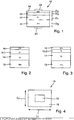
- FIG. 1 shows a view of a first embodiment of a stacked III-V semiconductor diode 10 according to the invention, comprising an n + substrate 12, a materially connected to the substrate 12 low-doped n - layer 14, a cohesively bonded to the n - layer 14 intermediate layer 16, one with the intermediate layer 16 cohesively connected p + layer 18 and a first contact 20 and a second contact 22.
- the first contact 20 is materially connected to a bottom of the n + substrate 12, while the second contact 22 cohesively with a Top of the p + layer 18 is connected.
- the n + substrate 12 is heavily n-doped and has a dopant concentration of 10 19 cm -3 .
- a layer thickness DS of the substrate 12 is between 100 ⁇ m and 400 ⁇ m.
- the n - -layer 16 is low n-doped with a dopant concentration of 10 12 -10 16 cm -3 and has a layer thickness D1 of 10-300 microns.
- the intermediate layer 14 has a layer thickness D3 of 1-50 ⁇ m and a low doping with a dopant concentration of 10 12 -10 17 cm -3 .
- the p + layer 18 is heavily p-doped with a dopant concentration of 10 19 cm -3 and a layer thickness D2 greater than 2 microns.
- FIGS. 2 and 3 are two alternative embodiments of one of the n + substrate 12, the n - layer 14, the intermediate layer 16 and the p + layer 18 existing layer structure shown 100 of a III-V semiconductor diode according to the invention. The following are just the differences from the illustration of FIG. 1 explained.
- the layer structure 100 may, according to a first embodiment, have a low p-doped intermediate layer 16. 1, as in FIG FIG. 2 shown.
- the Schlraumate has a low n-doped intermediate layer 16.2, as in FIG. 3 shown.
- FIGS. 4 In the picture of the FIGS. 4 is a watch on the in FIG. 1 shown first embodiment of a III-V semiconductor diode according to the invention. The following are just the differences from the illustration of FIG. 1 explained.
- the stacked layer structure 100 of the III-V semiconductor diode 10 consisting of the n + -type substrate 12, the n - -layer 14, the intermediate layer 16 and the p + -layer 18 has a rectangular circumference and thus also a rectangular surface with the edge lengths L1 and L2 on.
- the arranged on the surface of the layer sequence 100 contact surface 22 covers only a part of the surface.
- the stack also has a quadrangular surface.
- the surface is square.
- the corners are rounded in the angular embodiments in order to avoid field strength peaks at high voltages.
- the surface is made round. As a result, increases in field strength are particularly effectively reduced.
- the surface is circular or oval.
Landscapes
- Electrodes Of Semiconductors (AREA)
- Recrystallisation Techniques (AREA)
Priority Applications (1)
| Application Number | Priority Date | Filing Date | Title |
|---|---|---|---|
| EP19000090.1A EP3514837B1 (fr) | 2016-11-14 | 2017-11-10 | Diode semi-conductrice iii-v |
Applications Claiming Priority (1)
| Application Number | Priority Date | Filing Date | Title |
|---|---|---|---|
| DE102016013540.9A DE102016013540A1 (de) | 2016-11-14 | 2016-11-14 | lll-V-Halbleiterdiode |
Related Child Applications (2)
| Application Number | Title | Priority Date | Filing Date |
|---|---|---|---|
| EP19000090.1A Division EP3514837B1 (fr) | 2016-11-14 | 2017-11-10 | Diode semi-conductrice iii-v |
| EP19000090.1A Division-Into EP3514837B1 (fr) | 2016-11-14 | 2017-11-10 | Diode semi-conductrice iii-v |
Publications (2)
| Publication Number | Publication Date |
|---|---|
| EP3321971A1 true EP3321971A1 (fr) | 2018-05-16 |
| EP3321971B1 EP3321971B1 (fr) | 2019-10-23 |
Family
ID=60320616
Family Applications (2)
| Application Number | Title | Priority Date | Filing Date |
|---|---|---|---|
| EP17001844.4A Active EP3321971B1 (fr) | 2016-11-14 | 2017-11-10 | Diode semi-conductrice iii-v |
| EP19000090.1A Active EP3514837B1 (fr) | 2016-11-14 | 2017-11-10 | Diode semi-conductrice iii-v |
Family Applications After (1)
| Application Number | Title | Priority Date | Filing Date |
|---|---|---|---|
| EP19000090.1A Active EP3514837B1 (fr) | 2016-11-14 | 2017-11-10 | Diode semi-conductrice iii-v |
Country Status (5)
| Country | Link |
|---|---|
| US (1) | US10263124B2 (fr) |
| EP (2) | EP3321971B1 (fr) |
| JP (2) | JP6771131B2 (fr) |
| CN (1) | CN108074970B (fr) |
| DE (1) | DE102016013540A1 (fr) |
Families Citing this family (17)
| Publication number | Priority date | Publication date | Assignee | Title |
|---|---|---|---|---|
| DE102019001459B3 (de) | 2019-03-04 | 2020-09-03 | 3-5 Power Electronics GmbH | Stapelförmige hochsperrende III-V-Leistungshalbleiterdiode |
| CN109817728B (zh) * | 2019-03-20 | 2023-12-01 | 河北工业大学 | 一种pin二极管器件结构及其制备方法 |
| DE102019003068A1 (de) * | 2019-04-30 | 2020-11-05 | 3-5 Power Electronics GmbH | Stapelförmige hochsperrende lnGaAS-Halbleiterleistungsdiode |
| DE102019003069B4 (de) | 2019-04-30 | 2023-06-01 | Azur Space Solar Power Gmbh | Stapelförmige hochsperrende lll-V-Halbleiterleistungsdioden |
| CN110571283A (zh) * | 2019-08-29 | 2019-12-13 | 厦门市三安集成电路有限公司 | 半导体器件及半导体器件制作方法 |
| DE102019008927B4 (de) * | 2019-12-20 | 2024-04-11 | Azur Space Solar Power Gmbh | Gasphasenepitaxieverfahren |
| DE102019008931B4 (de) * | 2019-12-20 | 2024-04-11 | Azur Space Solar Power Gmbh | Gasphasenepitaxieverfahren |
| DE102020001841B4 (de) | 2020-03-20 | 2025-02-20 | Azur Space Solar Power Gmbh | Stapelförmige hochsperrende III-V-Halbleiterleistungsdiode |
| DE102020001838A1 (de) | 2020-03-20 | 2021-09-23 | Azur Space Solar Power Gmbh | Stapelförmige hochsperrende lll-V-Halbleiterleistungsdiode |
| DE102020001842A1 (de) | 2020-03-20 | 2021-09-23 | Azur Space Solar Power Gmbh | Stapelförmiges photonisches III-V-Halbleiterbauelement |
| DE102020001837B3 (de) | 2020-03-20 | 2021-08-26 | Azur Space Solar Power Gmbh | Stapelförmiges photonisches lll-V-Halbleiterbauelement |
| DE102020001835A1 (de) | 2020-03-20 | 2021-09-23 | Azur Space Solar Power Gmbh | Stapelförmige hochsperrende lll-V-Halbleiterleistungsdiode |
| DE102020001840B3 (de) | 2020-03-20 | 2021-09-23 | Azur Space Solar Power Gmbh | Stapelförmiges photonisches III-V-Halbleiterbauelement |
| DE102020001843A1 (de) | 2020-03-20 | 2021-09-23 | Azur Space Solar Power Gmbh | Stapelförmige hochsperrende InGaAs-Halbleiterleistungsdiode |
| DE102021000611A1 (de) | 2021-02-08 | 2022-08-11 | 3-5 Power Electronics GmbH | Stapelförmige III-V-Halbleiterdiode |
| DE102021000609A1 (de) | 2021-02-08 | 2022-08-11 | 3-5 Power Electronics GmbH | Stapelförmige III-V-Halbleiterdiode |
| DE102021000610A1 (de) | 2021-02-08 | 2022-08-11 | 3-5 Power Electronics GmbH | Stapelförmige III-V-Halbleiterdiode |
Citations (3)
| Publication number | Priority date | Publication date | Assignee | Title |
|---|---|---|---|---|
| US5733815A (en) * | 1992-05-22 | 1998-03-31 | Ramot University Authority For Applied Research & Industrial Development Ltd. | Process for fabricating intrinsic layer and applications |
| CN203118957U (zh) * | 2012-09-27 | 2013-08-07 | 宁波比亚迪半导体有限公司 | 一种快恢复二极管 |
| DE102015208097A1 (de) * | 2015-04-30 | 2016-11-03 | Infineon Technologies Ag | Herstellen einer Halbleitervorrichtung durch Epitaxie |
Family Cites Families (19)
| Publication number | Priority date | Publication date | Assignee | Title |
|---|---|---|---|---|
| JPS4634657Y1 (fr) | 1967-03-23 | 1971-11-30 | ||
| JPS49106780A (fr) * | 1973-02-12 | 1974-10-09 | ||
| SU511794A1 (ru) * | 1973-05-28 | 1976-10-05 | Предприятие П/Я А-1172 | Способ получени полупроводниковой светоизлучающей структуры |
| JPS5368084A (en) * | 1976-11-29 | 1978-06-17 | Fujitsu Ltd | Semiconductor device |
| FR2395605A1 (fr) * | 1977-06-21 | 1979-01-19 | Thomson Csf | Structure de diode a avalanche a rendement ameliore et diode utilisant une telle structure |
| JPS61161760A (ja) * | 1985-01-10 | 1986-07-22 | Matsushita Electronics Corp | 半導体装置の製造方法 |
| JPH0770474B2 (ja) * | 1985-02-08 | 1995-07-31 | 株式会社東芝 | 化合物半導体装置の製造方法 |
| JPH0618276B2 (ja) * | 1988-11-11 | 1994-03-09 | サンケン電気株式会社 | 半導体装置 |
| US5038187A (en) * | 1989-12-01 | 1991-08-06 | Hewlett-Packard Company | Pseudomorphic MODFET structure having improved linear power performance at microwave frequencies |
| JP2884376B2 (ja) * | 1990-10-25 | 1999-04-19 | サンケン電気株式会社 | 金属酸化物抵抗体の形成方法 |
| DE4036222A1 (de) * | 1990-11-14 | 1992-05-21 | Bosch Gmbh Robert | Verfahren zur herstellung von halbleiterelementen, insbesondere von dioden |
| IL105952A (en) * | 1993-06-08 | 1997-02-18 | Univ Ramot | Controlled semiconductor capacitors |
| JP2874596B2 (ja) * | 1995-06-09 | 1999-03-24 | 日本電気株式会社 | モノリシック電圧制御発振器 |
| JP2001015769A (ja) * | 1999-07-02 | 2001-01-19 | Fuji Electric Co Ltd | 高耐圧半導体装置 |
| JP4162439B2 (ja) * | 2002-07-19 | 2008-10-08 | アンリツ株式会社 | 半導体集積回路 |
| KR102288118B1 (ko) * | 2012-02-23 | 2021-08-11 | 센서 일렉트로닉 테크놀로지, 인크 | 반도체에 대한 오믹 접촉부 |
| CN202601620U (zh) * | 2012-03-11 | 2012-12-12 | 深圳市立德电控科技有限公司 | 快恢复二极管 |
| CN103700712B (zh) * | 2012-09-27 | 2017-05-03 | 比亚迪股份有限公司 | 一种快恢复二极管的结构及其制造方法 |
| CN103681992A (zh) * | 2014-01-07 | 2014-03-26 | 苏州晶湛半导体有限公司 | 半导体衬底、半导体器件及半导体衬底制造方法 |
-
2016
- 2016-11-14 DE DE102016013540.9A patent/DE102016013540A1/de not_active Withdrawn
-
2017
- 2017-11-10 EP EP17001844.4A patent/EP3321971B1/fr active Active
- 2017-11-10 EP EP19000090.1A patent/EP3514837B1/fr active Active
- 2017-11-13 JP JP2017218544A patent/JP6771131B2/ja active Active
- 2017-11-14 CN CN201711122731.3A patent/CN108074970B/zh active Active
- 2017-11-14 US US15/812,432 patent/US10263124B2/en active Active
-
2020
- 2020-06-12 JP JP2020102700A patent/JP7030348B2/ja active Active
Patent Citations (3)
| Publication number | Priority date | Publication date | Assignee | Title |
|---|---|---|---|---|
| US5733815A (en) * | 1992-05-22 | 1998-03-31 | Ramot University Authority For Applied Research & Industrial Development Ltd. | Process for fabricating intrinsic layer and applications |
| CN203118957U (zh) * | 2012-09-27 | 2013-08-07 | 宁波比亚迪半导体有限公司 | 一种快恢复二极管 |
| DE102015208097A1 (de) * | 2015-04-30 | 2016-11-03 | Infineon Technologies Ag | Herstellen einer Halbleitervorrichtung durch Epitaxie |
Non-Patent Citations (1)
| Title |
|---|
| BHOJANI RITESHKUMAR ET AL: "Gallium arsenide semiconductor parameters extracted from pin diode measurements and simulations", IET POWER ELECTRO, IET, UK, vol. 9, no. 4, 30 March 2016 (2016-03-30), pages 689 - 697, XP006055844, ISSN: 1755-4535, DOI: 10.1049/IET-PEL.2015.0019 * |
Also Published As
| Publication number | Publication date |
|---|---|
| EP3514837B1 (fr) | 2020-06-03 |
| JP7030348B2 (ja) | 2022-03-07 |
| JP2020141154A (ja) | 2020-09-03 |
| CN108074970A (zh) | 2018-05-25 |
| JP2018082174A (ja) | 2018-05-24 |
| US10263124B2 (en) | 2019-04-16 |
| EP3321971B1 (fr) | 2019-10-23 |
| US20180138320A1 (en) | 2018-05-17 |
| EP3514837A1 (fr) | 2019-07-24 |
| DE102016013540A1 (de) | 2018-05-17 |
| JP6771131B2 (ja) | 2020-10-21 |
| CN108074970B (zh) | 2021-09-07 |
Similar Documents
| Publication | Publication Date | Title |
|---|---|---|
| EP3321971B1 (fr) | Diode semi-conductrice iii-v | |
| EP3321970A1 (fr) | Diode semi-conductrice iii-v | |
| EP3379581B1 (fr) | Diode semi-conductrice iii-v à base de gaas | |
| EP3379577B1 (fr) | Diode semi-conductrice iii-v à base de gaas | |
| EP3522233B1 (fr) | Diode à semi-conduceur iii-v sous forme d'empilement | |
| DE112011103230B4 (de) | Non-Punch-Through-Bipolarleistungshalbleiterbauelement und ein Verfahren zum Herstellen eines derartigen Halbleiterbauelements | |
| EP3503204B1 (fr) | Composant à semi-conducteurs iii-v | |
| EP3336906A1 (fr) | Procédé de fabrication d'un empilement de couches en un substrat p+, d'une couche p, d'une couche n et d'une troisième couche | |
| EP3343636B1 (fr) | Structure semi-conductrice igbt | |
| EP3553827B1 (fr) | Composant à semi-conducteur iii-v sous forme d'empilement | |
| DE102011006492B3 (de) | Schottky-Diode und Herstellungsverfahren hierzu | |
| EP3734667B1 (fr) | Diode empilée de puissance à semi-conducteurs iii-v à blocage haute | |
| EP3321972B1 (fr) | Diode schottky empilée | |
| DE102019003068A1 (de) | Stapelförmige hochsperrende lnGaAS-Halbleiterleistungsdiode | |
| DE102018009132A1 (de) | Asymmetrisches transientes Spannungsunterdrückungs-Bauelement und Verfahren zur Bildung | |
| DE102017209590B4 (de) | Halbleiterdiode | |
| EP3882980A2 (fr) | Diode empilée de puissance à semi-conducteur iii-v à blocage haut | |
| DE102020001841A1 (de) | Stapelförmige hochsperrende III-V-Halbleiterleistungsdiode | |
| DE102020001835A1 (de) | Stapelförmige hochsperrende lll-V-Halbleiterleistungsdiode |
Legal Events
| Date | Code | Title | Description |
|---|---|---|---|
| PUAI | Public reference made under article 153(3) epc to a published international application that has entered the european phase |
Free format text: ORIGINAL CODE: 0009012 |
|
| STAA | Information on the status of an ep patent application or granted ep patent |
Free format text: STATUS: THE APPLICATION HAS BEEN PUBLISHED |
|
| STAA | Information on the status of an ep patent application or granted ep patent |
Free format text: STATUS: REQUEST FOR EXAMINATION WAS MADE |
|
| AK | Designated contracting states |
Kind code of ref document: A1 Designated state(s): AL AT BE BG CH CY CZ DE DK EE ES FI FR GB GR HR HU IE IS IT LI LT LU LV MC MK MT NL NO PL PT RO RS SE SI SK SM TR |
|
| AX | Request for extension of the european patent |
Extension state: BA ME |
|
| 17P | Request for examination filed |
Effective date: 20180425 |
|
| RBV | Designated contracting states (corrected) |
Designated state(s): AL AT BE BG CH CY CZ DE DK EE ES FI FR GB GR HR HU IE IS IT LI LT LU LV MC MK MT NL NO PL PT RO RS SE SI SK SM TR |
|
| STAA | Information on the status of an ep patent application or granted ep patent |
Free format text: STATUS: EXAMINATION IS IN PROGRESS |
|
| 17Q | First examination report despatched |
Effective date: 20181211 |
|
| GRAP | Despatch of communication of intention to grant a patent |
Free format text: ORIGINAL CODE: EPIDOSNIGR1 |
|
| STAA | Information on the status of an ep patent application or granted ep patent |
Free format text: STATUS: GRANT OF PATENT IS INTENDED |
|
| RIC1 | Information provided on ipc code assigned before grant |
Ipc: H01L 29/861 20060101AFI20190618BHEP Ipc: H01L 21/18 20060101ALI20190618BHEP Ipc: H01L 29/207 20060101ALI20190618BHEP Ipc: H01L 21/329 20060101ALI20190618BHEP Ipc: H01L 29/36 20060101ALI20190618BHEP Ipc: H01L 29/06 20060101ALN20190618BHEP |
|
| INTG | Intention to grant announced |
Effective date: 20190703 |
|
| GRAS | Grant fee paid |
Free format text: ORIGINAL CODE: EPIDOSNIGR3 |
|
| GRAA | (expected) grant |
Free format text: ORIGINAL CODE: 0009210 |
|
| STAA | Information on the status of an ep patent application or granted ep patent |
Free format text: STATUS: THE PATENT HAS BEEN GRANTED |
|
| AK | Designated contracting states |
Kind code of ref document: B1 Designated state(s): AL AT BE BG CH CY CZ DE DK EE ES FI FR GB GR HR HU IE IS IT LI LT LU LV MC MK MT NL NO PL PT RO RS SE SI SK SM TR |
|
| REG | Reference to a national code |
Ref country code: GB Ref legal event code: FG4D Free format text: NOT ENGLISH |
|
| REG | Reference to a national code |
Ref country code: CH Ref legal event code: EP |
|
| REG | Reference to a national code |
Ref country code: IE Ref legal event code: FG4D Free format text: LANGUAGE OF EP DOCUMENT: GERMAN |
|
| REG | Reference to a national code |
Ref country code: DE Ref legal event code: R096 Ref document number: 502017002610 Country of ref document: DE |
|
| REG | Reference to a national code |
Ref country code: AT Ref legal event code: REF Ref document number: 1194667 Country of ref document: AT Kind code of ref document: T Effective date: 20191115 |
|
| REG | Reference to a national code |
Ref country code: CH Ref legal event code: NV Representative=s name: KIRKER AND CIE S.A., CH |
|
| REG | Reference to a national code |
Ref country code: NL Ref legal event code: MP Effective date: 20191023 |
|
| REG | Reference to a national code |
Ref country code: LT Ref legal event code: MG4D |
|
| PG25 | Lapsed in a contracting state [announced via postgrant information from national office to epo] |
Ref country code: PT Free format text: LAPSE BECAUSE OF FAILURE TO SUBMIT A TRANSLATION OF THE DESCRIPTION OR TO PAY THE FEE WITHIN THE PRESCRIBED TIME-LIMIT Effective date: 20200224 Ref country code: NO Free format text: LAPSE BECAUSE OF FAILURE TO SUBMIT A TRANSLATION OF THE DESCRIPTION OR TO PAY THE FEE WITHIN THE PRESCRIBED TIME-LIMIT Effective date: 20200123 Ref country code: PL Free format text: LAPSE BECAUSE OF FAILURE TO SUBMIT A TRANSLATION OF THE DESCRIPTION OR TO PAY THE FEE WITHIN THE PRESCRIBED TIME-LIMIT Effective date: 20191023 Ref country code: GR Free format text: LAPSE BECAUSE OF FAILURE TO SUBMIT A TRANSLATION OF THE DESCRIPTION OR TO PAY THE FEE WITHIN THE PRESCRIBED TIME-LIMIT Effective date: 20200124 Ref country code: NL Free format text: LAPSE BECAUSE OF FAILURE TO SUBMIT A TRANSLATION OF THE DESCRIPTION OR TO PAY THE FEE WITHIN THE PRESCRIBED TIME-LIMIT Effective date: 20191023 Ref country code: LT Free format text: LAPSE BECAUSE OF FAILURE TO SUBMIT A TRANSLATION OF THE DESCRIPTION OR TO PAY THE FEE WITHIN THE PRESCRIBED TIME-LIMIT Effective date: 20191023 Ref country code: LV Free format text: LAPSE BECAUSE OF FAILURE TO SUBMIT A TRANSLATION OF THE DESCRIPTION OR TO PAY THE FEE WITHIN THE PRESCRIBED TIME-LIMIT Effective date: 20191023 Ref country code: SE Free format text: LAPSE BECAUSE OF FAILURE TO SUBMIT A TRANSLATION OF THE DESCRIPTION OR TO PAY THE FEE WITHIN THE PRESCRIBED TIME-LIMIT Effective date: 20191023 Ref country code: FI Free format text: LAPSE BECAUSE OF FAILURE TO SUBMIT A TRANSLATION OF THE DESCRIPTION OR TO PAY THE FEE WITHIN THE PRESCRIBED TIME-LIMIT Effective date: 20191023 Ref country code: BG Free format text: LAPSE BECAUSE OF FAILURE TO SUBMIT A TRANSLATION OF THE DESCRIPTION OR TO PAY THE FEE WITHIN THE PRESCRIBED TIME-LIMIT Effective date: 20200123 |
|
| PGFP | Annual fee paid to national office [announced via postgrant information from national office to epo] |
Ref country code: IE Payment date: 20200204 Year of fee payment: 3 |
|
| PG25 | Lapsed in a contracting state [announced via postgrant information from national office to epo] |
Ref country code: RS Free format text: LAPSE BECAUSE OF FAILURE TO SUBMIT A TRANSLATION OF THE DESCRIPTION OR TO PAY THE FEE WITHIN THE PRESCRIBED TIME-LIMIT Effective date: 20191023 Ref country code: HR Free format text: LAPSE BECAUSE OF FAILURE TO SUBMIT A TRANSLATION OF THE DESCRIPTION OR TO PAY THE FEE WITHIN THE PRESCRIBED TIME-LIMIT Effective date: 20191023 Ref country code: IS Free format text: LAPSE BECAUSE OF FAILURE TO SUBMIT A TRANSLATION OF THE DESCRIPTION OR TO PAY THE FEE WITHIN THE PRESCRIBED TIME-LIMIT Effective date: 20200224 |
|
| PG25 | Lapsed in a contracting state [announced via postgrant information from national office to epo] |
Ref country code: AL Free format text: LAPSE BECAUSE OF FAILURE TO SUBMIT A TRANSLATION OF THE DESCRIPTION OR TO PAY THE FEE WITHIN THE PRESCRIBED TIME-LIMIT Effective date: 20191023 |
|
| REG | Reference to a national code |
Ref country code: DE Ref legal event code: R097 Ref document number: 502017002610 Country of ref document: DE |
|
| PG2D | Information on lapse in contracting state deleted |
Ref country code: IS |
|
| PG25 | Lapsed in a contracting state [announced via postgrant information from national office to epo] |
Ref country code: DK Free format text: LAPSE BECAUSE OF FAILURE TO SUBMIT A TRANSLATION OF THE DESCRIPTION OR TO PAY THE FEE WITHIN THE PRESCRIBED TIME-LIMIT Effective date: 20191023 Ref country code: LU Free format text: LAPSE BECAUSE OF NON-PAYMENT OF DUE FEES Effective date: 20191110 Ref country code: MC Free format text: LAPSE BECAUSE OF FAILURE TO SUBMIT A TRANSLATION OF THE DESCRIPTION OR TO PAY THE FEE WITHIN THE PRESCRIBED TIME-LIMIT Effective date: 20191023 Ref country code: CZ Free format text: LAPSE BECAUSE OF FAILURE TO SUBMIT A TRANSLATION OF THE DESCRIPTION OR TO PAY THE FEE WITHIN THE PRESCRIBED TIME-LIMIT Effective date: 20191023 Ref country code: EE Free format text: LAPSE BECAUSE OF FAILURE TO SUBMIT A TRANSLATION OF THE DESCRIPTION OR TO PAY THE FEE WITHIN THE PRESCRIBED TIME-LIMIT Effective date: 20191023 Ref country code: ES Free format text: LAPSE BECAUSE OF FAILURE TO SUBMIT A TRANSLATION OF THE DESCRIPTION OR TO PAY THE FEE WITHIN THE PRESCRIBED TIME-LIMIT Effective date: 20191023 Ref country code: RO Free format text: LAPSE BECAUSE OF FAILURE TO SUBMIT A TRANSLATION OF THE DESCRIPTION OR TO PAY THE FEE WITHIN THE PRESCRIBED TIME-LIMIT Effective date: 20191023 Ref country code: IS Free format text: LAPSE BECAUSE OF FAILURE TO SUBMIT A TRANSLATION OF THE DESCRIPTION OR TO PAY THE FEE WITHIN THE PRESCRIBED TIME-LIMIT Effective date: 20200223 |
|
| PLBE | No opposition filed within time limit |
Free format text: ORIGINAL CODE: 0009261 |
|
| STAA | Information on the status of an ep patent application or granted ep patent |
Free format text: STATUS: NO OPPOSITION FILED WITHIN TIME LIMIT |
|
| PG25 | Lapsed in a contracting state [announced via postgrant information from national office to epo] |
Ref country code: SK Free format text: LAPSE BECAUSE OF FAILURE TO SUBMIT A TRANSLATION OF THE DESCRIPTION OR TO PAY THE FEE WITHIN THE PRESCRIBED TIME-LIMIT Effective date: 20191023 Ref country code: SM Free format text: LAPSE BECAUSE OF FAILURE TO SUBMIT A TRANSLATION OF THE DESCRIPTION OR TO PAY THE FEE WITHIN THE PRESCRIBED TIME-LIMIT Effective date: 20191023 Ref country code: IT Free format text: LAPSE BECAUSE OF FAILURE TO SUBMIT A TRANSLATION OF THE DESCRIPTION OR TO PAY THE FEE WITHIN THE PRESCRIBED TIME-LIMIT Effective date: 20191023 |
|
| 26N | No opposition filed |
Effective date: 20200724 |
|
| PG25 | Lapsed in a contracting state [announced via postgrant information from national office to epo] |
Ref country code: SI Free format text: LAPSE BECAUSE OF FAILURE TO SUBMIT A TRANSLATION OF THE DESCRIPTION OR TO PAY THE FEE WITHIN THE PRESCRIBED TIME-LIMIT Effective date: 20191023 |
|
| PG25 | Lapsed in a contracting state [announced via postgrant information from national office to epo] |
Ref country code: CY Free format text: LAPSE BECAUSE OF FAILURE TO SUBMIT A TRANSLATION OF THE DESCRIPTION OR TO PAY THE FEE WITHIN THE PRESCRIBED TIME-LIMIT Effective date: 20191023 |
|
| PG25 | Lapsed in a contracting state [announced via postgrant information from national office to epo] |
Ref country code: HU Free format text: LAPSE BECAUSE OF FAILURE TO SUBMIT A TRANSLATION OF THE DESCRIPTION OR TO PAY THE FEE WITHIN THE PRESCRIBED TIME-LIMIT; INVALID AB INITIO Effective date: 20171110 Ref country code: MT Free format text: LAPSE BECAUSE OF FAILURE TO SUBMIT A TRANSLATION OF THE DESCRIPTION OR TO PAY THE FEE WITHIN THE PRESCRIBED TIME-LIMIT Effective date: 20191023 |
|
| PG25 | Lapsed in a contracting state [announced via postgrant information from national office to epo] |
Ref country code: IE Free format text: LAPSE BECAUSE OF NON-PAYMENT OF DUE FEES Effective date: 20201110 |
|
| PG25 | Lapsed in a contracting state [announced via postgrant information from national office to epo] |
Ref country code: TR Free format text: LAPSE BECAUSE OF FAILURE TO SUBMIT A TRANSLATION OF THE DESCRIPTION OR TO PAY THE FEE WITHIN THE PRESCRIBED TIME-LIMIT Effective date: 20191023 |
|
| PG25 | Lapsed in a contracting state [announced via postgrant information from national office to epo] |
Ref country code: MK Free format text: LAPSE BECAUSE OF FAILURE TO SUBMIT A TRANSLATION OF THE DESCRIPTION OR TO PAY THE FEE WITHIN THE PRESCRIBED TIME-LIMIT Effective date: 20191023 |
|
| REG | Reference to a national code |
Ref country code: AT Ref legal event code: MM01 Ref document number: 1194667 Country of ref document: AT Kind code of ref document: T Effective date: 20221110 |
|
| PG25 | Lapsed in a contracting state [announced via postgrant information from national office to epo] |
Ref country code: AT Free format text: LAPSE BECAUSE OF NON-PAYMENT OF DUE FEES Effective date: 20221110 |
|
| GBPC | Gb: european patent ceased through non-payment of renewal fee |
Effective date: 20231110 |
|
| REG | Reference to a national code |
Ref country code: GB Ref legal event code: S28 Free format text: APPLICATION FILED |
|
| PG25 | Lapsed in a contracting state [announced via postgrant information from national office to epo] |
Ref country code: GB Free format text: LAPSE BECAUSE OF NON-PAYMENT OF DUE FEES Effective date: 20231110 |
|
| PG25 | Lapsed in a contracting state [announced via postgrant information from national office to epo] |
Ref country code: GB Free format text: LAPSE BECAUSE OF NON-PAYMENT OF DUE FEES Effective date: 20231110 |
|
| REG | Reference to a national code |
Ref country code: GB Ref legal event code: S28 Free format text: RESTORATION ALLOWED Effective date: 20241030 |
|
| REG | Reference to a national code |
Ref country code: DE Ref legal event code: R079 Ref document number: 502017002610 Country of ref document: DE Free format text: PREVIOUS MAIN CLASS: H01L0029861000 Ipc: H10D0008000000 |
|
| REG | Reference to a national code |
Ref country code: CH Ref legal event code: U11 Free format text: ST27 STATUS EVENT CODE: U-0-0-U10-U11 (AS PROVIDED BY THE NATIONAL OFFICE) Effective date: 20251201 |
|
| PGFP | Annual fee paid to national office [announced via postgrant information from national office to epo] |
Ref country code: DE Payment date: 20251119 Year of fee payment: 9 |
|
| PGFP | Annual fee paid to national office [announced via postgrant information from national office to epo] |
Ref country code: GB Payment date: 20251121 Year of fee payment: 9 |
|
| PGFP | Annual fee paid to national office [announced via postgrant information from national office to epo] |
Ref country code: FR Payment date: 20251121 Year of fee payment: 9 |
|
| PGFP | Annual fee paid to national office [announced via postgrant information from national office to epo] |
Ref country code: BE Payment date: 20251119 Year of fee payment: 9 |
|
| PGFP | Annual fee paid to national office [announced via postgrant information from national office to epo] |
Ref country code: CH Payment date: 20251201 Year of fee payment: 9 |