EP3376281A1 - Film de régulation de lumière et vitre feuilletée - Google Patents
Film de régulation de lumière et vitre feuilletée Download PDFInfo
- Publication number
- EP3376281A1 EP3376281A1 EP16864364.1A EP16864364A EP3376281A1 EP 3376281 A1 EP3376281 A1 EP 3376281A1 EP 16864364 A EP16864364 A EP 16864364A EP 3376281 A1 EP3376281 A1 EP 3376281A1
- Authority
- EP
- European Patent Office
- Prior art keywords
- liquid crystal
- spacer
- light control
- control film
- laminate
- Prior art date
- Legal status (The legal status is an assumption and is not a legal conclusion. Google has not performed a legal analysis and makes no representation as to the accuracy of the status listed.)
- Granted
Links
Images






Classifications
-
- G—PHYSICS
- G02—OPTICS
- G02F—OPTICAL DEVICES OR ARRANGEMENTS FOR THE CONTROL OF LIGHT BY MODIFICATION OF THE OPTICAL PROPERTIES OF THE MEDIA OF THE ELEMENTS INVOLVED THEREIN; NON-LINEAR OPTICS; FREQUENCY-CHANGING OF LIGHT; OPTICAL LOGIC ELEMENTS; OPTICAL ANALOGUE/DIGITAL CONVERTERS
- G02F1/00—Devices or arrangements for the control of the intensity, colour, phase, polarisation or direction of light arriving from an independent light source, e.g. switching, gating or modulating; Non-linear optics
- G02F1/01—Devices or arrangements for the control of the intensity, colour, phase, polarisation or direction of light arriving from an independent light source, e.g. switching, gating or modulating; Non-linear optics for the control of the intensity, phase, polarisation or colour
- G02F1/13—Devices or arrangements for the control of the intensity, colour, phase, polarisation or direction of light arriving from an independent light source, e.g. switching, gating or modulating; Non-linear optics for the control of the intensity, phase, polarisation or colour based on liquid crystals, e.g. single liquid crystal display cells
- G02F1/133—Constructional arrangements; Operation of liquid crystal cells; Circuit arrangements
- G02F1/1333—Constructional arrangements; Manufacturing methods
- G02F1/1339—Gaskets; Spacers; Sealing of cells
-
- G—PHYSICS
- G02—OPTICS
- G02F—OPTICAL DEVICES OR ARRANGEMENTS FOR THE CONTROL OF LIGHT BY MODIFICATION OF THE OPTICAL PROPERTIES OF THE MEDIA OF THE ELEMENTS INVOLVED THEREIN; NON-LINEAR OPTICS; FREQUENCY-CHANGING OF LIGHT; OPTICAL LOGIC ELEMENTS; OPTICAL ANALOGUE/DIGITAL CONVERTERS
- G02F1/00—Devices or arrangements for the control of the intensity, colour, phase, polarisation or direction of light arriving from an independent light source, e.g. switching, gating or modulating; Non-linear optics
- G02F1/01—Devices or arrangements for the control of the intensity, colour, phase, polarisation or direction of light arriving from an independent light source, e.g. switching, gating or modulating; Non-linear optics for the control of the intensity, phase, polarisation or colour
- G02F1/13—Devices or arrangements for the control of the intensity, colour, phase, polarisation or direction of light arriving from an independent light source, e.g. switching, gating or modulating; Non-linear optics for the control of the intensity, phase, polarisation or colour based on liquid crystals, e.g. single liquid crystal display cells
- G02F1/133—Constructional arrangements; Operation of liquid crystal cells; Circuit arrangements
- G02F1/1333—Constructional arrangements; Manufacturing methods
- G02F1/1339—Gaskets; Spacers; Sealing of cells
- G02F1/13394—Gaskets; Spacers; Sealing of cells spacers regularly patterned on the cell subtrate, e.g. walls, pillars
-
- E—FIXED CONSTRUCTIONS
- E06—DOORS, WINDOWS, SHUTTERS, OR ROLLER BLINDS IN GENERAL; LADDERS
- E06B—FIXED OR MOVABLE CLOSURES FOR OPENINGS IN BUILDINGS, VEHICLES, FENCES OR LIKE ENCLOSURES IN GENERAL, e.g. DOORS, WINDOWS, BLINDS, GATES
- E06B3/00—Window sashes, door leaves, or like elements for closing wall or like openings; Layout of fixed or moving closures, e.g. windows in wall or like openings; Features of rigidly-mounted outer frames relating to the mounting of wing frames
- E06B3/66—Units comprising two or more parallel glass or like panes permanently secured together
- E06B3/67—Units comprising two or more parallel glass or like panes permanently secured together characterised by additional arrangements or devices for heat or sound insulation or for controlled passage of light
- E06B3/6715—Units comprising two or more parallel glass or like panes permanently secured together characterised by additional arrangements or devices for heat or sound insulation or for controlled passage of light specially adapted for increased thermal insulation or for controlled passage of light
- E06B3/6722—Units comprising two or more parallel glass or like panes permanently secured together characterised by additional arrangements or devices for heat or sound insulation or for controlled passage of light specially adapted for increased thermal insulation or for controlled passage of light with adjustable passage of light
-
- E—FIXED CONSTRUCTIONS
- E06—DOORS, WINDOWS, SHUTTERS, OR ROLLER BLINDS IN GENERAL; LADDERS
- E06B—FIXED OR MOVABLE CLOSURES FOR OPENINGS IN BUILDINGS, VEHICLES, FENCES OR LIKE ENCLOSURES IN GENERAL, e.g. DOORS, WINDOWS, BLINDS, GATES
- E06B9/00—Screening or protective devices for wall or similar openings, with or without operating or securing mechanisms; Closures of similar construction
- E06B9/24—Screens or other constructions affording protection against light, especially against sunshine; Similar screens for privacy or appearance; Slat blinds
-
- G—PHYSICS
- G02—OPTICS
- G02F—OPTICAL DEVICES OR ARRANGEMENTS FOR THE CONTROL OF LIGHT BY MODIFICATION OF THE OPTICAL PROPERTIES OF THE MEDIA OF THE ELEMENTS INVOLVED THEREIN; NON-LINEAR OPTICS; FREQUENCY-CHANGING OF LIGHT; OPTICAL LOGIC ELEMENTS; OPTICAL ANALOGUE/DIGITAL CONVERTERS
- G02F1/00—Devices or arrangements for the control of the intensity, colour, phase, polarisation or direction of light arriving from an independent light source, e.g. switching, gating or modulating; Non-linear optics
- G02F1/01—Devices or arrangements for the control of the intensity, colour, phase, polarisation or direction of light arriving from an independent light source, e.g. switching, gating or modulating; Non-linear optics for the control of the intensity, phase, polarisation or colour
- G02F1/13—Devices or arrangements for the control of the intensity, colour, phase, polarisation or direction of light arriving from an independent light source, e.g. switching, gating or modulating; Non-linear optics for the control of the intensity, phase, polarisation or colour based on liquid crystals, e.g. single liquid crystal display cells
- G02F1/133—Constructional arrangements; Operation of liquid crystal cells; Circuit arrangements
- G02F1/1333—Constructional arrangements; Manufacturing methods
- G02F1/1337—Surface-induced orientation of the liquid crystal molecules, e.g. by alignment layers
-
- G—PHYSICS
- G02—OPTICS
- G02F—OPTICAL DEVICES OR ARRANGEMENTS FOR THE CONTROL OF LIGHT BY MODIFICATION OF THE OPTICAL PROPERTIES OF THE MEDIA OF THE ELEMENTS INVOLVED THEREIN; NON-LINEAR OPTICS; FREQUENCY-CHANGING OF LIGHT; OPTICAL LOGIC ELEMENTS; OPTICAL ANALOGUE/DIGITAL CONVERTERS
- G02F1/00—Devices or arrangements for the control of the intensity, colour, phase, polarisation or direction of light arriving from an independent light source, e.g. switching, gating or modulating; Non-linear optics
- G02F1/01—Devices or arrangements for the control of the intensity, colour, phase, polarisation or direction of light arriving from an independent light source, e.g. switching, gating or modulating; Non-linear optics for the control of the intensity, phase, polarisation or colour
- G02F1/13—Devices or arrangements for the control of the intensity, colour, phase, polarisation or direction of light arriving from an independent light source, e.g. switching, gating or modulating; Non-linear optics for the control of the intensity, phase, polarisation or colour based on liquid crystals, e.g. single liquid crystal display cells
- G02F1/133—Constructional arrangements; Operation of liquid crystal cells; Circuit arrangements
- G02F1/1333—Constructional arrangements; Manufacturing methods
- G02F1/1339—Gaskets; Spacers; Sealing of cells
- G02F1/13392—Gaskets; Spacers; Sealing of cells spacers dispersed on the cell substrate, e.g. spherical particles, microfibres
-
- G—PHYSICS
- G02—OPTICS
- G02F—OPTICAL DEVICES OR ARRANGEMENTS FOR THE CONTROL OF LIGHT BY MODIFICATION OF THE OPTICAL PROPERTIES OF THE MEDIA OF THE ELEMENTS INVOLVED THEREIN; NON-LINEAR OPTICS; FREQUENCY-CHANGING OF LIGHT; OPTICAL LOGIC ELEMENTS; OPTICAL ANALOGUE/DIGITAL CONVERTERS
- G02F1/00—Devices or arrangements for the control of the intensity, colour, phase, polarisation or direction of light arriving from an independent light source, e.g. switching, gating or modulating; Non-linear optics
- G02F1/01—Devices or arrangements for the control of the intensity, colour, phase, polarisation or direction of light arriving from an independent light source, e.g. switching, gating or modulating; Non-linear optics for the control of the intensity, phase, polarisation or colour
- G02F1/13—Devices or arrangements for the control of the intensity, colour, phase, polarisation or direction of light arriving from an independent light source, e.g. switching, gating or modulating; Non-linear optics for the control of the intensity, phase, polarisation or colour based on liquid crystals, e.g. single liquid crystal display cells
- G02F1/137—Devices or arrangements for the control of the intensity, colour, phase, polarisation or direction of light arriving from an independent light source, e.g. switching, gating or modulating; Non-linear optics for the control of the intensity, phase, polarisation or colour based on liquid crystals, e.g. single liquid crystal display cells characterised by the electro-optical or magneto-optical effect, e.g. field-induced phase transition, orientation effect, guest-host interaction or dynamic scattering
- G02F1/13725—Devices or arrangements for the control of the intensity, colour, phase, polarisation or direction of light arriving from an independent light source, e.g. switching, gating or modulating; Non-linear optics for the control of the intensity, phase, polarisation or colour based on liquid crystals, e.g. single liquid crystal display cells characterised by the electro-optical or magneto-optical effect, e.g. field-induced phase transition, orientation effect, guest-host interaction or dynamic scattering based on guest-host interaction
-
- B—PERFORMING OPERATIONS; TRANSPORTING
- B60—VEHICLES IN GENERAL
- B60J—WINDOWS, WINDSCREENS, NON-FIXED ROOFS, DOORS, OR SIMILAR DEVICES FOR VEHICLES; REMOVABLE EXTERNAL PROTECTIVE COVERINGS SPECIALLY ADAPTED FOR VEHICLES
- B60J1/00—Windows; Windscreens; Accessories therefor
- B60J1/001—Double glazing for vehicles
-
- B—PERFORMING OPERATIONS; TRANSPORTING
- B60—VEHICLES IN GENERAL
- B60J—WINDOWS, WINDSCREENS, NON-FIXED ROOFS, DOORS, OR SIMILAR DEVICES FOR VEHICLES; REMOVABLE EXTERNAL PROTECTIVE COVERINGS SPECIALLY ADAPTED FOR VEHICLES
- B60J3/00—Antiglare equipment associated with windows or windscreens; Sun visors for vehicles
- B60J3/04—Antiglare equipment associated with windows or windscreens; Sun visors for vehicles adjustable in transparency
-
- E—FIXED CONSTRUCTIONS
- E06—DOORS, WINDOWS, SHUTTERS, OR ROLLER BLINDS IN GENERAL; LADDERS
- E06B—FIXED OR MOVABLE CLOSURES FOR OPENINGS IN BUILDINGS, VEHICLES, FENCES OR LIKE ENCLOSURES IN GENERAL, e.g. DOORS, WINDOWS, BLINDS, GATES
- E06B9/00—Screening or protective devices for wall or similar openings, with or without operating or securing mechanisms; Closures of similar construction
- E06B9/24—Screens or other constructions affording protection against light, especially against sunshine; Similar screens for privacy or appearance; Slat blinds
- E06B2009/2417—Light path control; means to control reflection
-
- E—FIXED CONSTRUCTIONS
- E06—DOORS, WINDOWS, SHUTTERS, OR ROLLER BLINDS IN GENERAL; LADDERS
- E06B—FIXED OR MOVABLE CLOSURES FOR OPENINGS IN BUILDINGS, VEHICLES, FENCES OR LIKE ENCLOSURES IN GENERAL, e.g. DOORS, WINDOWS, BLINDS, GATES
- E06B9/00—Screening or protective devices for wall or similar openings, with or without operating or securing mechanisms; Closures of similar construction
- E06B9/24—Screens or other constructions affording protection against light, especially against sunshine; Similar screens for privacy or appearance; Slat blinds
- E06B2009/2464—Screens or other constructions affording protection against light, especially against sunshine; Similar screens for privacy or appearance; Slat blinds featuring transparency control by applying voltage, e.g. LCD, electrochromic panels
-
- G—PHYSICS
- G02—OPTICS
- G02F—OPTICAL DEVICES OR ARRANGEMENTS FOR THE CONTROL OF LIGHT BY MODIFICATION OF THE OPTICAL PROPERTIES OF THE MEDIA OF THE ELEMENTS INVOLVED THEREIN; NON-LINEAR OPTICS; FREQUENCY-CHANGING OF LIGHT; OPTICAL LOGIC ELEMENTS; OPTICAL ANALOGUE/DIGITAL CONVERTERS
- G02F1/00—Devices or arrangements for the control of the intensity, colour, phase, polarisation or direction of light arriving from an independent light source, e.g. switching, gating or modulating; Non-linear optics
- G02F1/01—Devices or arrangements for the control of the intensity, colour, phase, polarisation or direction of light arriving from an independent light source, e.g. switching, gating or modulating; Non-linear optics for the control of the intensity, phase, polarisation or colour
- G02F1/13—Devices or arrangements for the control of the intensity, colour, phase, polarisation or direction of light arriving from an independent light source, e.g. switching, gating or modulating; Non-linear optics for the control of the intensity, phase, polarisation or colour based on liquid crystals, e.g. single liquid crystal display cells
- G02F1/133—Constructional arrangements; Operation of liquid crystal cells; Circuit arrangements
- G02F1/1333—Constructional arrangements; Manufacturing methods
- G02F1/1339—Gaskets; Spacers; Sealing of cells
- G02F1/13398—Spacer materials; Spacer properties
Definitions
- the present invention relates to a light control film that can be used in, for example, an electronic blind controlling the transmission of extraneous light by being bonded to a window or the like, and laminated glass in which the light control film is used.
- Such light control films include a light control film using liquid crystals.
- the light control film using liquid crystals is produced by sandwiching a liquid crystal cell with linear polarizing plates, the liquid crystal cell being produced by sandwiching a liquid crystal material with transparent plate materials in which transparent electrodes are produced. Accordingly, this light control film performs blocking or transmission of extraneous light by changing the alignment of the liquid crystals through a change in an electric field applied to the liquid crystals, and changes an amount of the transmitted light, so that the transmission of extraneous light is controlled.
- the light control film is configured such that a spacer is provided in the transparent plate materials constituting the liquid crystal cell and the thickness of the liquid crystal layer is kept constant by the spacer.
- alignment layers are produced from thin films such as polyimide to which rubbing treatment is applied after the spacer is produced, and the alignment of the liquid crystals is regulated by the alignment layers.
- the light control film is used as an intermediate material of laminated glass or the like.
- the pressing force at a time when the intermediate material is sandwiched and integrated with glass plates causes the electrodes to be short-circuited between the transparent plate materials constituting the liquid crystal cell or the gap (cell gap) between the transparent plate materials to become non-uniform. Accordingly, problems arise in the form of unstable driving and a reduction in quality of external appearance.
- the light control film is used when being bonded to a pane of glass or the like as well as in the laminated glass as described above. The same problems arise in this case depending on the conditions of use as in the case described above.
- an object of the invention is to, for example, effectively avoid a reduction in quality of external appearance to perform stable driving sufficiently, and also prevent diffracted light from being visually recognized by effectively avoiding a reduction in transmittance and a deterioration in liquid crystal alignment.
- the inventors of the present invention have intensively studied to solve the above-mentioned problems and the like and completed the present invention by reaching an idea to optimize the area of a spacer per unit area.
- the present invention When the light control film using the liquid crystals is used as an intermediate material of laminated glass and the like, it is possible for the present invention to, for example, effectively avoid a reduction in quality of external appearance to perform sufficiently stable driving, and prevent diffracted light from being visually recognized by effectively avoiding a reduction in transmittance and a deterioration in liquid crystal alignment.
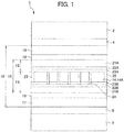
- Fig. 1 is a sectional view illustrating laminated glass according to a first embodiment of the present invention.
- This laminated glass 1 is applied to a vehicle window or the like and includes a light control film 10 which is sandwiched by plate glass 2 and plate glass 3 via an intermediate layer 4 and an intermediate layer 5, respectively.
- Various materials applicable to this type of laminated glass can be widely applied to the plate glass 2 and the plate glass 3.
- the intermediate layers 4 and 5 functions as adhesive layers between the light control film 10 and the plate glass 2 and 3.
- Various elements applied to this type of laminated glass can be widely applied to the intermediate layers 4 and 5, and the intermediate layers 4 and 5 may function as, for example, heat ray shielding materials.
- the plate glass 2 is laminated with the light control film 10 via the intermediate layer 4, and the plate glass 3 is laminated with the light control film 10 via the intermediate layer 5, respectively. Subsequently, the laminated glass 1 is heated and pressurized such that the plate glass 2 and 3 are integrated with the light control film 10 via the intermediate layers 4 and 5, and given a desired curved surface shape as a whole. Accordingly, the laminated glass 1 is applicable to a rear window of a vehicle or the like, and is configured to control transmitted light by the light control film 10.
- processes for manufacturing the laminated glass 1 include a lamination process in which the light control film 10 is laminated with the plate glass 2 provided with the intermediate layer 4 and the plate glass 3 provided with the intermediate layer 5 and a heating, and pressurization and heating process in which the laminate resulting from the lamination process is heated and pressurized.
- Fig. 2 is a sectional view illustrating the light control film.
- This light control film 10 is formed in a film shape and is used for a light-controlling part, for example, as well as for laminated glass. Usage cases where the light control film 10 is bonded to the light controlling part include, for example, a case where switching between transparency and opacity is performed with the light control film 10 disposed on window glass of a building, a showcase, a transparent indoor partition, and the like.
- This light control film 10 is a light control film controlling transmitted light by using liquid crystals.
- a liquid crystal cell 15 is produced by a liquid crystal layer 14 being sandwiched by a lower laminate 13 (first laminate) and an upper laminate 12 (second laminate) that are film-shaped first and second laminates.
- the light control film 10 is produced by the liquid crystal cell 15 being sandwiched by linear polarizers 16 and 17.
- a twisted nematic (TN) method is applied for driving of the liquid crystal layer 14 in this embodiment
- various methods are applicable such as a vertical alignment (VA) method and an in-place-switching (IPS) method.
- VA vertical alignment
- IPS in-place-switching
- the lower laminate 13 and/or the upper laminate 12 is provided with spacers 24 so that a thickness of the liquid crystal layer 14 is maintained constant.
- the linear polarizers 16 and 17 are provided with retardation films 18 and 19 for optical compensation, each of which is provided on a liquid crystal cell 15 side, respectively.
- the laminates 12 and 13 are formed by sequential creation of electrodes 22A and 22B and alignment layers 23A and 23B on base materials 21A and 21B, respectively.
- the retardation films 18 and 19 may be omitted if unnecessary.
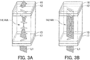
- This light control film 10 is configured to switch between a transparent state and a non-transparent state, by changing voltages applied to the electrodes 22A and 22B such that the transmission of extraneous light L1 is controlled as illustrated in Figs. 3A and 3B.
- Fig. 3A illustrates a state where no voltage is applied between the electrodes 22A and 22B.
- Fig. 3(B) illustrates a state where a voltage is applied to the electrodes 22A and 22B.
- the liquid crystal layer 14 is driven by so-called normally white in this embodiment.
- the liquid crystal layer 14 may alternatively be driven by normally black.
- the electrodes 22A and 22B are produced together on an alignment layer 23A side or an alignment layer 23B side and the laminates 12 and 13 (described later) are configured accordingly when the IPS method is applied.
- a protective layer of a hard coat layer or the like is provided on a surface of the linear polarizer 16 and/or 17 that is on a side opposite to the liquid crystal cell 15.
- the base materials 21A and 21B can be adopted as the base materials 21A and 21B, and a polycarbonate-based film material on both surfaces of which are provided with hard coat layer is applied in this embodiment.
- Various elements perceived as transparent are applicable to the electrodes 22A and 22B which are capable of applying a substantially uniform electric field to the liquid crystal layer 14.
- the electrodes 22A and 22B are formed in such a manner that the entire surfaces of the base materials 21A and 21B are covered respectively with a transparent conductive film made of an ITO of a transparent electrode material.
- the electrodes are produced through patterning in a desired shape.
- alignment layers 23A and 23B Various material layers applicable to alignment layers such as polyimide are adopted as the alignment layers 23A and 23B.
- the alignment layers 23A and 23B are formed in such a manner that a finely lined uneven shape is produced in surfaces of the material layers through rubbing treatment with a rubbing roll. It may be appropriate that the alignment layers through the rubbing treatment- described above may be replaced with alignment layers which are produced in such an alternative manner that the finely lined uneven shape produced by the rubbing treatment is produced instead by shaping treatment or by means of a photo-alignment layer.
- a spacer 24 according to this embodiment is produced of photoresist material although various resin materials are widely applicable.
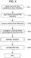
- Fig. 4 is a flowchart illustrating a process for manufacturing the liquid crystal cell 15.
- the ITO-based transparent electrodes 22A and 22B are produced on the base materials 21A and 21B of the liquid crystal cell 15.
- a coating liquid (photoresist) pertaining to the spacer 24 is applied, and then the spacer 24 is produced through drying, exposure, and development.
- the spacer production process SP3 is omitted for the base material in which the spacer 24 is not produced.
- an alignment layer material layer production process SP4 for the liquid crystal cell the material layers of the alignment layers 23A and 23B are formed by a coating liquid pertaining to the alignment layers 23A and 23B being applied, dried, and cured.
- a rubbing process SP5 for the liquid crystal cell a finely lined uneven shape is produced in the surfaces of the alignment layer material layers through rubbing roll-based rubbing treatment and the alignment layers 23A and 23B are produced as a result.
- the sealant 25 shaped to surround the liquid crystal layer 14 is provided for one of the laminates 12 and 13, and a liquid crystal material is disposed in the place that is surrounded by the sealant 25.
- lamination is performed by the other one of the laminates 12 and 13 being brought in this state such that the liquid crystal material is sandwiched by the laminates 12 and 13, the sealant is cured by ultraviolet irradiation or the like with pressurization performed in this state, and the liquid crystal cell 15 is produced accordingly.
- the liquid crystal cell 15 is provided in the form of a long film in which the base materials 21A and 21B are wound around a roll, and some or all of the processes SP2 to SP6 are executed while the base materials 21A and 21B are unwound from the roll and transported. As a result, each process for the liquid crystal cell 15 is executed by processing per a sheet from midway of processes if necessary.
- Fig. 5 is a chart showing the configuration of the spacer 24 in detail.
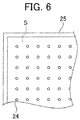
- Fig. 6 is a diagram illustrating a part of the cross section taken along line A-A of Fig. 2 . As illustrated in Fig. 6 , the spacers 24 are disposed in an internal region that is surrounded by the sealant 25. The internal region is a light control region S contributing to light control of the light control film 1.
- Each spacer 24 has a circular cross section resulting from a columnar shape, more specifically a cylindrical shape or a truncated cone shape.
- the spacers 24 are disposed such that the proportion of an area occupied by the spacers 24 per unit area in the light control region S when the light control film 10 is viewed from the front (proportion of the projected area of the spacers 24 when viewed from one surface of the light control film 10, hereinafter, appropriately referred to as the occupancy of the spacer) is 0.5% to 10% inclusive and more preferably 0.5% to 8% inclusive.
- the spacers 24 may be deformed due to the pressurization and heating in the heating and pressurization process among processes for manufacturing the laminated glass 1.
- the electrodes 22A and 22B of the laminates 12 and 13 may be short-circuited to be inoperable, or may operate unstably in the light control film 10.
- a thickness (cell gap) of the liquid crystal layer 14 locally decreases and becomes non-uniform, resulting in a reduction in quality of external appearance.
- the pressure acting on each spacer increases to cause the spacer 24 to crush, a tip of the spacer 24 to penetrate a facing surface to cause the electrode to be short-circuited, and the base material to bend between the spacers 24 to result in the non-uniformity of the cell gap, such that the operation of the light control film becomes unstable and the quality of external appearance decreases accordingly, when the occupancy of the spacer is less than 0.5%.
- the short circuit of the electrodes 22A and 22B and the local cell gap reduction attributable to the deformation of the spacer 24 can be prevented and a reduction in the quality of external appearance can be prevented based on a stable operation as a result.
- parts of the light control film 10 where the spacers 24 are provided block transmitted light by the optical properties of the laminate of the linear polarizers 16 and 17 based on cross-Nicol arrangement.
- Fig. 5 is a chart specifically illustrating the results of experiments regarding the occupancy of the spacers.
- "X" indicates that a measurement result not suitable for practical use was obtained in every sample
- " ⁇ ” indicates that a measurement result not suitable for practical use was obtained in some of a plurality of samples
- " ⁇ ” indicates that a sufficiently practical measurement result was obtained in each of the samples.
- weight corresponding to 0.8 MPa was applied to the light control film for 24 hours in a state where the light control film was placed on a smooth and highly hard surface of a surface plate. Subsequently, cell gaps were observed to know bending of the base material between the spacers and cell gap non-uniformity (bending, non-uniform thickness).
- the upper laminate and the lower laminate were peeled off and crushing of the spacers (spacer crushing) was confirmed through microscopic spacer observation.
- spacer tip penetration at a spacer-abutting part and deformation (film penetration and base material deformation) of the base material were observed through microscopic observation of the spacer-abutting part.
- transmitted light was observed to know a reduction in transmittance (transparency), the degree of diffracted light (transmitted light diffraction), and liquid crystal alignment.
- the voltage applied to the electrode was switched to perform switching between a transmission state and a light blocking state, so that the drivability of liquid crystals (liquid crystal drivability) was observed. Furthermore, the external appearance was observed.
- Comparative Example 1 in Fig. 5 spacers each having a diameter of 7 ⁇ m and a height of 6 ⁇ m were produced and disposed at equal pitches of 110 ⁇ m in two orthogonal directions.
- a spacer with a diameter of 7 ⁇ m was disposed within an area of 110 ⁇ 110 ⁇ m 2 .
- a light control film was produced with a liquid crystal cell produced at spacer occupancy of 0.3%.
- Comparative Example 1 a reduction in transmittance attributable to the spacer 24 was negligibly small and an amount of the diffracted light in the transmitted light was also small as a result of the 0.3% spacer occupancy. In addition, it was found that local liquid crystal misalignment was almost negligible. However, the region with a non-uniform cell gap resulting from base material bending between the spacers 24 still existed. Accordingly, a problem in terms of liquid crystal drivability remained since it was difficult to set an entire surface uniformly in a light blocking state and a translucent state through driving a liquid crystal layer 14. A poor appearance was also confirmed. As an overall evaluation, it has been found that this Comparative Example 1 is not suitable for practical use.
- Example 1 spacers 24 each having a diameter of 9 ⁇ m and a height of 6 ⁇ m were disposed at a pitch of 110 ⁇ m with spacer occupancy of 0.5%.
- Example 2 spacers 24 each having a diameter of 27 ⁇ m and a height of 6 ⁇ m were disposed at a pitch of 230 ⁇ m with spacer occupancy of 1%.
- Example 3 spacers 24 each having a diameter of 28 ⁇ m and a height of 6 ⁇ m were disposed at a pitch of 110 ⁇ m with spacer occupancy of 5%.
- Example 4 spacers 24 each having a diameter of 35 ⁇ m and a height of 6 ⁇ m were disposed at a pitch of 110 ⁇ m with spacer occupancy of 8%.
- Example 5 spacers 24 with a diameter of 39 ⁇ m and a height of 6 ⁇ m were disposed at a pitch of 110 ⁇ m with spacer occupancy of 10%.
- the spacer 24 is given a height corresponding to the thickness required of the liquid crystal layer 14 depending on the liquid crystal material used for the liquid crystal layer 14. More specifically, the height of the spacer 24 is 2 to 10 ⁇ m inclusive.
- the spacers 24 are randomly disposed in some cases. In such cases, the occupancy of the spacers is obtained by calculation of the area of a part where the spacers 24 are disposed in a region with a sufficiently large area. That is, the occupancy of the spacers is obtained by a summation of sectional areas of the spacers 24 disposed at the part in a plan view (front view).
- the spacer 24 is formed in a substantially circular shape (with an ellipticity of at least 0.9) in a front view in which the tip is a flat surface.
- a change in the size of the part that creates the shadow in the rubbing treatment can be reduced with respect to any rubbing treatment direction. Accordingly, various products with different rubbing directions can be stably produced.
- the spacer 24 When the spacer 24 is formed in the substantially circular shape in the front view in which the tip is a flat surface as described above, it is possible to reduce stress concentration at the tip of the spacer 24. Accordingly, it is possible to avoid a phenomenon in which the tip of the spacer 24 pierces a facing alignment layer and cell gap non-uniformity attributable to crushing of the spacer 24 occurs during liquid crystal cell production.
- the spacer 24 When the spacer 24 is produced with an ellipticity of at least 0.9, local stress concentration can be sufficiently mitigated and a reduction in quality of external appearance and the like can be avoided even more effectively, by producing the spacer 24 in such a manner that a diameter of at least 9 ⁇ m on the minor axis side and the above-described occupancy are satisfied.
- an occupancy of 0.5 to 10% is satisfied as a whole, it may be that any area of 1 mm 2 in the light control region S satisfies 0.5 to 10% range.
- an area of 1 mm 2 within an easily stressed part at least satisfies the occupancy of 0.5 to 10%.
- Other parts having less than this occupancy may be present in a place where stress is relatively less likely to act.
- the number of the spacers 24 disposed within a range with a radius of 200 ⁇ m in the light control region S is 2 to 30 inclusive and more preferably 2 to 10 inclusive.
- the pressure acting on each spacer increases similarly with the above-described case where the occupancy of the spacer 24 is less than 0.5%. Accordingly, the spacer 24 is crushed or the tip of the spacer 24 penetrates a facing surface to cause the electrode to be short-circuited. In addition, the cell gap becomes non-uniform due to the base material being bent between the spacers 24, the operation of the light control film becomes unstable and the quality of external appearance decreases.
- the short circuit of the electrodes 22A and 22B and the local cell gap reduction attributable to the deformation of the spacer 24 can be prevented and the reduction in the quality of external appearance can be prevented based on a stable operation as a result.
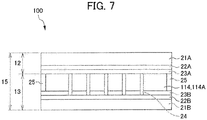
- Fig. 7 is a sectional view illustrating a light control film 100 according to a second embodiment.
- the second embodiment differs from the first embodiment in that a liquid crystal layer 114 according to the second embodiment is a guest-host method one in which dichroic dyes are mixed with guest-host type liquid crystal molecules 114A.
- the guest-host method is a method by which dichroic dyes 114B are mixed in the guest-host type liquid crystal molecules 114A. Light transmission and blocking are controlled by the dichroic dyes 114B which moves along with a movement of the guest-host type liquid crystal molecules 114A.
- Fig. 7 is identical to Fig. 2 except that no linear polarizer is provided, and thus the same reference numerals will be used to refer to members common to Figs. 2 and 7 so that the same description is not repeated.
- Figs. 8 and 9 are diagrams showing directions of the guest-host type liquid crystal molecules 114A and the dichroic dyes 114B in the guest-host method liquid crystal layer 114.
- the guest-host method light control film 100 blocks light
- the guest-host type liquid crystal molecules 114A and the dichroic dyes 114B are horizontally aligned in one direction as illustrated in Fig. 8 .
- production is performed such that the longitudinal directions of the liquid crystal composition and the dichroic dyes 114B are the same horizontal direction.
- the guest-host liquid crystals and the dichroic dyes 114B are vertically aligned as illustrated in Fig. 9 .
- longitudinal directions of a liquid crystal composition and the dichroic dyes 114B become a thickness direction of the liquid crystal layer 114.
- a spacer 24 is disposed such that an occupancy per unit area in a light control region S when the light control film 100 is seen in a front view is 0.5% to 10% inclusive and more, preferably 0.5% to 8% inclusive.
- the occupancy of the spacer is 0.5% or more, and thus the short circuit of electrodes 22A and 22B and a local cell gap reduction attributable to the deformation of the spacer 24 can be prevented, and a reduction in quality of external appearance can be prevented as a result of a stable operation similarly with the first embodiment.
- a change in transmittance and a change in color with respect to gap fluctuation are smaller than in the light control film according to the first embodiment. Accordingly, a difference in transmittance and color unevenness are unlikely to be witnessed even when the gap (thickness of the liquid crystal layer 114) changes as a result of slight bending of the base material.
- the number of the spacers 24 disposed within the range with the radius of 200 ⁇ m in the light control region is 2 to 30 inclusive and preferably 2 to 10 inclusive in the first embodiment.
- the effect that a difference in transmittance and color unevenness are unlikely to be witnessed even when the gap (thickness of the liquid crystal layer 114) changes as a result of slight bending of the base material can be achieved with the number of spacers 24 within a range with a radius of 200 ⁇ m being 1 to 30 inclusive and preferably 1 to 10 inclusive.
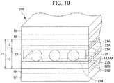
- Fig. 10 is a sectional perspective view illustrating a light control film 200 according to a third embodiment.
- a so-called bead spacers 224 are used as spacers.
- a bead spacer 224 according to the present embodiment has a spherical shape, and the diameter thereof is 1 ⁇ m to 20 ⁇ m and preferably ranges from 3 ⁇ m to 15 ⁇ m.
- the same reference numerals will be used to refer to members common to Figs. 2 and 10 so that the same description is not repeated.
- the bead spacer 224 is provided to control a thickness of a liquid crystal layer 14 similarly with the spacer 24 according to the first embodiment.
- a composition based on an inorganic material formed of silica or the like, an organic material-based composition, a composition using a core-shell structure in which those are combined and the like can be widely applied to the bead spacer 224.
- bead spacer 224 has a spherical shape
- alternative configurations may include a rod shape such as a cylindrical shape and a prismatic shape.
- the bead spacer 224 may be disposed anywhere between electrodes 22A and 22B.
- the bead spacer 224 is produced with a transparent member, colored material application and color adjustment may be also possible if necessary.
- the bead spacers 224 are randomly disposed on the electrode 22B and held in an almost immovable manner by a coating liquid resulting from dispersion of the bead spacers 224 and a resin component in a solvent being partially applied and then drying and baking being sequentially executed.
- a lower limit of the occupancy of the bead spacers 224 may be smaller than in the first embodiment and the lower limit is 0.1% to 10% inclusive and more preferably 0.2% to 8% inclusive in the present embodiment.
- 300 bead spacers are disposed in a unit area of 1 mm 2 (300 bead spacers/mm 2 ) with an occupancy of 0.32%.
- the bead spacer 224 according to the present embodiment may have a lower occupancy than the photoresist-based spacer 24 according to the first embodiment.
- the reason for this is that the number of supporting points becomes relatively large even at the same occupancy as the spacer 24 in the case of the bead spacer 224 although the number of supporting points tends to decrease as the diameter of the cylindrical shape exceeds the liquid crystal cell gap in the case of the spacer 24, with respect to the designed liquid crystal cell gap (that is, the height of the spacer 24 in the case of the spacer 24 and the diameter of the bead spacer 224 in the case of the bead spacer 224) .
- any range of 1 mm 2 in a light control region S satisfies this 0.5% to 10% range.
- the range of 1 mm 2 within an easily stressed part is at least 0.5% to 10%.
- Other parts less than this range may be present in a place where stress is relatively less likely to act.
- Fig. 11 is a diagram illustrating a dispersion state of the bead spacers 224.
- the bead spacers 224 according to the present embodiment are not regularly arranged because the bead spacers 224 are disposed by spraying not similarly with the case of the first embodiment in which drying, exposure, and development are performed after photoresist coating.
- the concentration and dispersion are adjusted in the present embodiment, such that the bead spacers 224 are arranged in such a manner as illustrated in Fig. 11 that at least one of the bead spacers 224 exists in any of regions A and B within a range of 200 ⁇ m from an arbitrary point located in a plane..
- Fig. 12 illustrates a comparative configuration in which a region B' exists where no spacer is present within a range of 200 ⁇ m from an arbitrary point in a plane.
- the gap may not be maintainable at a part where the light control film is bent.
- a region is not present where no spacer is present within the range of 200 ⁇ m from an arbitrary point in the plane, and thus the gap (thickness of the liquid crystal layer) can be maintained even at a part where the light control film 200 is bent.
- the present embodiment has the effects as shown below in addition to the effects of the first embodiment.
- the bead spacer 224 is used, and a bead spacer 224 is disposed in a state where the central axis thereof is horizontal. Accordingly, contact portions between the bead spacer 224 and alignment layers 23A and 23B remain close to a straight line and liquid crystal molecules 14A are present in gaps between the alignment layers 23A and 23B and the bead spacer 224 in a thickness direction of a liquid crystal layer 14. Since the liquid crystal molecules 14A existing in the gaps also contribute to light control, a light control function is not impaired in an entire area occupied by the spacers 224and a deterioration in the light control function can be reduced.
- the liquid crystal cell according to the third embodiment also may include a guest-host method one similarly with the case of the second embodiment.
- the spacer according to the embodiments described above is made of a transparent photoresist resin
- the present invention is not limited thereto. It may be alternatively possible to widely apply the present invention to cases where a spacer is produced by shaping treatment, integrally with or separately from an alignment layer, and by the use of resin provided for shaping of an ultraviolet-curable resin and the like.
Landscapes
- Physics & Mathematics (AREA)
- Nonlinear Science (AREA)
- Optics & Photonics (AREA)
- Crystallography & Structural Chemistry (AREA)
- Chemical & Material Sciences (AREA)
- General Physics & Mathematics (AREA)
- Mathematical Physics (AREA)
- Engineering & Computer Science (AREA)
- Structural Engineering (AREA)
- Spectroscopy & Molecular Physics (AREA)
- Civil Engineering (AREA)
- Liquid Crystal (AREA)
- Architecture (AREA)
- Joining Of Glass To Other Materials (AREA)
Priority Applications (1)
| Application Number | Priority Date | Filing Date | Title |
|---|---|---|---|
| EP24166939.9A EP4386475A3 (fr) | 2015-11-13 | 2016-11-11 | Film de commande de lumière et verre feuilleté |
Applications Claiming Priority (3)
| Application Number | Priority Date | Filing Date | Title |
|---|---|---|---|
| JP2015223394 | 2015-11-13 | ||
| JP2016210662A JP6213653B2 (ja) | 2015-11-13 | 2016-10-27 | 調光フィルム及び合わせガラス |
| PCT/JP2016/083568 WO2017082403A1 (fr) | 2015-11-13 | 2016-11-11 | Film de régulation de lumière et vitre feuilletée |
Related Child Applications (1)
| Application Number | Title | Priority Date | Filing Date |
|---|---|---|---|
| EP24166939.9A Division EP4386475A3 (fr) | 2015-11-13 | 2016-11-11 | Film de commande de lumière et verre feuilleté |
Publications (3)
| Publication Number | Publication Date |
|---|---|
| EP3376281A1 true EP3376281A1 (fr) | 2018-09-19 |
| EP3376281A4 EP3376281A4 (fr) | 2019-05-08 |
| EP3376281B1 EP3376281B1 (fr) | 2024-04-24 |
Family
ID=58817752
Family Applications (1)
| Application Number | Title | Priority Date | Filing Date |
|---|---|---|---|
| EP16864364.1A Active EP3376281B1 (fr) | 2015-11-13 | 2016-11-11 | Film de régulation de lumière et vitre feuilletée |
Country Status (5)
| Country | Link |
|---|---|
| US (1) | US11809047B2 (fr) |
| EP (1) | EP3376281B1 (fr) |
| JP (7) | JP6213653B2 (fr) |
| KR (1) | KR102651739B1 (fr) |
| CN (1) | CN108463768A (fr) |
Families Citing this family (46)
| Publication number | Priority date | Publication date | Assignee | Title |
|---|---|---|---|---|
| CN109219770B (zh) * | 2016-06-20 | 2022-03-22 | 大日本印刷株式会社 | 调光膜、调光膜的驱动方法、调光构件、车辆 |
| WO2019004160A1 (fr) * | 2017-06-26 | 2019-01-03 | 大日本印刷株式会社 | Élément de modulation de lumière, pare-soleil et corps mobile |
| JP7147139B2 (ja) * | 2017-07-31 | 2022-10-05 | 大日本印刷株式会社 | 合わせガラスの製造方法 |
| KR20240064046A (ko) * | 2017-07-31 | 2024-05-10 | 다이니폰 인사츠 가부시키가이샤 | 접합 유리, 접합 유리의 제조 방법 |
| JP2019070780A (ja) * | 2017-10-11 | 2019-05-09 | 大日本印刷株式会社 | 調光フィルム、調光部材、車両 |
| JP7062912B2 (ja) * | 2017-10-11 | 2022-05-09 | 大日本印刷株式会社 | 調光フィルム、調光部材、車両、調光システム及び調光フィルムの駆動方法 |
| JP2019070781A (ja) * | 2017-10-11 | 2019-05-09 | 大日本印刷株式会社 | 調光フィルム、調光部材、車両 |
| KR102607588B1 (ko) | 2017-11-02 | 2023-11-30 | 다이니폰 인사츠 가부시키가이샤 | 접합 유리의 제조 방법, 접합 유리, 조광 필름 |
| JP7440266B2 (ja) * | 2017-11-24 | 2024-02-28 | 大日本印刷株式会社 | 合わせガラス、液晶フィルム |
| KR102184388B1 (ko) * | 2017-11-28 | 2020-11-30 | 주식회사 엘지화학 | 투과도 가변 장치 및 그 용도 |
| JP2019101375A (ja) * | 2017-12-07 | 2019-06-24 | 大日本印刷株式会社 | 調光フィルム、調光部材、車両 |
| US11644717B2 (en) | 2018-01-17 | 2023-05-09 | Sekisui Chemical Co., Ltd. | Dimming laminate and resin spacer for dimming laminate |
| KR102448828B1 (ko) | 2018-01-30 | 2022-09-29 | 다이니폰 인사츠 가부시키가이샤 | 액정 조광 장치 및 그 제조 방법 |
| US11695904B2 (en) | 2018-07-20 | 2023-07-04 | Dai Nippon Printing Co., Ltd. | Reflective screen and image display device |
| CN115857270A (zh) | 2018-07-20 | 2023-03-28 | 大日本印刷株式会社 | 反射屏幕和影像显示装置 |
| JP7228122B2 (ja) * | 2018-08-08 | 2023-02-24 | 大日本印刷株式会社 | 調光セルおよびその製造方法、ならびに調光装置およびその製造方法 |
| US20200089031A1 (en) * | 2018-09-19 | 2020-03-19 | Sharp Kabushiki Kaisha | Method of producing liquid crystal panel |
| JP2020064092A (ja) * | 2018-10-15 | 2020-04-23 | 三菱電機株式会社 | 立体表示装置 |
| JP7373124B2 (ja) * | 2019-01-25 | 2023-11-02 | 大日本印刷株式会社 | 調光装置及びその製造方法 |
| CN111983863B (zh) | 2019-05-24 | 2025-08-26 | 北京京东方晟视科技有限公司 | 调光玻璃 |
| US12206061B2 (en) * | 2019-07-30 | 2025-01-21 | Apple Inc. | Electronic device having display with internal light reflection suppression |
| JP7409125B2 (ja) * | 2020-02-04 | 2024-01-09 | 大日本印刷株式会社 | 調光装置及びその製造方法 |
| DE112021002330T5 (de) | 2020-06-25 | 2023-02-23 | Nippon Kayaku Kabushiki Kaisha | Anthrachinonverbindung, flüssigkristallzusammensetzung zum dimmen, die diese verbindung beinhaltet, und dimmelement |
| FR3114266B1 (fr) * | 2020-09-18 | 2022-11-18 | Saint Gobain | VITRAGE FEUILLETE A CRISTAUX LIQUIDES ET A COUPURE DANS l’UV |
| CN116420112B (zh) | 2020-10-29 | 2025-08-05 | 株式会社Lg化学 | 光学装置 |
| US11726379B2 (en) * | 2020-11-20 | 2023-08-15 | Wicue Usa Inc. | Liquid crystal assembly |
| EP4303646A4 (fr) * | 2021-03-05 | 2024-08-28 | Toppan Inc. | Feuille de commande de lumière et dispositif de commande de lumière |
| JP7810168B2 (ja) * | 2021-03-05 | 2026-02-03 | Toppanホールディングス株式会社 | 調光シート及び調光装置 |
| JP7787149B2 (ja) | 2021-03-11 | 2025-12-16 | 日本化薬株式会社 | アントラキノン化合物、該化合物を含有する液晶組成物、及び調光素子 |
| JP7558104B2 (ja) * | 2021-03-31 | 2024-09-30 | 株式会社ジャパンディスプレイ | 光学素子 |
| JP7723078B2 (ja) | 2021-04-14 | 2025-08-13 | 日本化薬株式会社 | アントラキノン化合物、該化合物を含む液晶組成物及び調光素子 |
| KR102471941B1 (ko) * | 2021-06-04 | 2022-11-29 | 동우 화인켐 주식회사 | 광학 적층체 및 이의 제조방법과, 이를 포함하는 스마트 윈도우 및 이를 적용한 자동차 또는 건물용 창호 |
| KR102533622B1 (ko) * | 2021-06-24 | 2023-05-17 | 동우 화인켐 주식회사 | 광학 적층체 및 이의 제조방법과, 이를 포함하는 스마트 윈도우 및 이를 적용한 자동차 또는 건물용 창호 |
| EP4369083A4 (fr) * | 2021-07-05 | 2025-06-25 | Dai Nippon Printing Co., Ltd. | Élément de commande de lumière et dispositif de commande de lumière |
| WO2023283335A1 (fr) | 2021-07-07 | 2023-01-12 | Genesis Systems Llc | Revêtement de surface pour auvent et système de génération et de stockage d'énergie électrique |
| KR102950070B1 (ko) * | 2021-07-16 | 2026-04-08 | 동우 화인켐 주식회사 | 광학 적층체 및 이의 제조방법과, 이를 포함하는 스마트 윈도우 및 이를 적용한 자동차 또는 건물용 창호 |
| WO2023054962A1 (fr) * | 2021-09-28 | 2023-04-06 | 동우 화인켐 주식회사 | Stratifié optique, son procédé de fabrication, fenêtre intelligente le comprenant, et fenêtre ou porte de véhicule et bâtiment l'utilisant |
| KR102763778B1 (ko) * | 2021-09-28 | 2025-02-07 | 동우 화인켐 주식회사 | 광학 적층체 및 이의 제조방법과, 이를 포함하는 스마트 윈도우 및 이를 적용한 자동차 또는 건물용 창호 |
| US12312294B2 (en) | 2021-10-14 | 2025-05-27 | Nippon Kayaku Kabushiki Kaisha | Anthraquinone compound, liquid crystal composition containing said compound, and dimming element |
| TW202330882A (zh) | 2021-11-04 | 2023-08-01 | 日商日本化藥股份有限公司 | 蒽醌化合物、含該化合物的液晶組成物及調光元件 |
| JP7401038B2 (ja) | 2021-11-19 | 2023-12-19 | 大日本印刷株式会社 | 合わせガラス及び液晶装置 |
| WO2023100848A1 (fr) | 2021-12-01 | 2023-06-08 | 日本化薬株式会社 | Composé d'anthraquinone, composition de cristaux liquides contenant ledit composé et élément de gradation |
| KR102909396B1 (ko) * | 2022-03-17 | 2026-01-08 | 동우 화인켐 주식회사 | 광학 적층체 및 이의 제조방법과, 이를 포함하는 스마트 윈도우 |
| KR102763783B1 (ko) * | 2022-04-28 | 2025-02-07 | 동우 화인켐 주식회사 | 투과율 가변 광학 적층체 및 이의 제조방법과, 이를 포함하는 스마트 윈도우 |
| KR102740412B1 (ko) * | 2022-07-01 | 2024-12-10 | 동우 화인켐 주식회사 | 투과율 가변 광학 적층체 및 이를 포함하는 스마트 윈도우 |
| CN119916616A (zh) * | 2025-03-20 | 2025-05-02 | 北京京东方晟视科技有限公司 | 液晶调光滤镜及调光装置 |
Family Cites Families (40)
| Publication number | Priority date | Publication date | Assignee | Title |
|---|---|---|---|---|
| JPH0347392A (ja) | 1989-07-12 | 1991-02-28 | Natl House Ind Co Ltd | 液晶パネル |
| JPH03158827A (ja) * | 1989-11-17 | 1991-07-08 | I C I Japan Kk | 液晶表示素子の製造方法 |
| JPH0451221A (ja) | 1990-06-20 | 1992-02-19 | Ricoh Co Ltd | 液晶表示素子 |
| JPH04293016A (ja) | 1991-03-22 | 1992-10-16 | Seiko Instr Inc | 液晶装置 |
| JPH04366921A (ja) | 1991-06-14 | 1992-12-18 | Toyota Motor Corp | 振動板付き液晶表示素子 |
| JPH06175139A (ja) * | 1992-12-09 | 1994-06-24 | Teijin Ltd | プラスチック基板液晶表示素子およびその製造方法 |
| JPH06273727A (ja) | 1993-03-18 | 1994-09-30 | Sumitomo Electric Ind Ltd | 液晶素子およびその製造方法 |
| JPH0720479A (ja) | 1993-07-02 | 1995-01-24 | Sumitomo Electric Ind Ltd | 液晶素子およびその製造方法 |
| JPH08184273A (ja) | 1994-12-27 | 1996-07-16 | Ohbayashi Corp | 調光ガラス窓 |
| JPH11119227A (ja) * | 1997-10-13 | 1999-04-30 | Hitachi Ltd | 液晶表示装置 |
| JP3760645B2 (ja) | 1998-11-11 | 2006-03-29 | コニカミノルタホールディングス株式会社 | 液晶光変調デバイスの製造方法 |
| US6396559B1 (en) * | 1998-11-17 | 2002-05-28 | Sharp Kabushiki Kaisha | LCD including spacers used in combination with polymer walls |
| EP1072931A3 (fr) | 1999-07-27 | 2002-02-13 | Minolta Co., Ltd. | Dispositif d'affichage à cristaux liquides et procédé de fabrication d'un dispositif d'affichage à cristaux liquides |
| JP2001042349A (ja) | 1999-07-27 | 2001-02-16 | Minolta Co Ltd | 液晶表示素子 |
| JP2001142083A (ja) * | 1999-11-17 | 2001-05-25 | Sanyo Electric Co Ltd | 表示装置の製造方法及び表示装置 |
| JP2004070069A (ja) * | 2002-08-07 | 2004-03-04 | Ricoh Co Ltd | 積層基板の製造方法・積層型液晶表示素子の製造方法 |
| JP4432356B2 (ja) | 2003-04-30 | 2010-03-17 | ソニー株式会社 | 調光装置及び撮像装置 |
| US20050068629A1 (en) | 2003-09-26 | 2005-03-31 | Primal Fernando | Adjustably opaque window |
| WO2006077838A1 (fr) | 2005-01-20 | 2006-07-27 | Sharp Kabushiki Kaisha | Element d'affichage a cristaux liquides |
| JP2007010843A (ja) | 2005-06-29 | 2007-01-18 | Hitachi Displays Ltd | 液晶表示パネル |
| KR20070079141A (ko) | 2006-02-01 | 2007-08-06 | 삼성전자주식회사 | 표시패널, 이의 제조방법 및 이를 제조하는 데 사용되는스페이서 인쇄장치 |
| TW200815879A (en) * | 2006-09-19 | 2008-04-01 | Ind Tech Res Inst | Liquid crystal EO film with particles having high surface area and method of fabricating the same |
| JP2008102341A (ja) * | 2006-10-19 | 2008-05-01 | Fujifilm Corp | 調光材料 |
| JP2008256993A (ja) * | 2007-04-06 | 2008-10-23 | Hitachi Displays Ltd | 液晶表示素子とその製造方法 |
| JP2010208861A (ja) | 2007-07-03 | 2010-09-24 | Asahi Glass Co Ltd | 調光窓材 |
| JP2009036967A (ja) | 2007-08-01 | 2009-02-19 | Asahi Glass Co Ltd | 調光窓材 |
| JP2009216976A (ja) | 2008-03-11 | 2009-09-24 | Epson Imaging Devices Corp | 液晶装置、液晶装置の製造方法及び電子機器 |
| TWI370934B (en) * | 2008-05-08 | 2012-08-21 | Au Optronics Corp | Liquid crystal panel structure and method for manufacturing the same |
| WO2010022294A2 (fr) * | 2008-08-20 | 2010-02-25 | Ravenbrick, Llc | Procédés de fabrication de filtres thermochromes |
| JP2011186453A (ja) | 2010-02-12 | 2011-09-22 | Semiconductor Energy Lab Co Ltd | 液晶表示装置 |
| CN101957521B (zh) | 2010-08-12 | 2013-11-20 | 大连东方科脉电子有限公司 | 一种液晶电子纸显示器及其制造方法 |
| JP2012150206A (ja) | 2011-01-18 | 2012-08-09 | Japan Display Central Co Ltd | 液晶シャッタ |
| JP2014149319A (ja) | 2011-06-03 | 2014-08-21 | Sharp Corp | 表示装置 |
| JP5951202B2 (ja) | 2011-08-23 | 2016-07-13 | スタンレー電気株式会社 | 液晶表示装置 |
| JP2013130746A (ja) * | 2011-12-22 | 2013-07-04 | Seiko Electric Co Ltd | 調光素子 |
| CN104583849B (zh) * | 2012-08-27 | 2017-07-18 | 夏普株式会社 | 液晶显示装置 |
| KR20150109339A (ko) | 2012-11-21 | 2015-10-01 | 넥세온 에너지 솔루션즈 엘엘씨 | 에너지 효율화 필름 |
| CN102967967B (zh) * | 2012-12-14 | 2014-12-17 | 福耀玻璃工业集团股份有限公司 | 一种用于调光体间隔粒子的粘接层的粘结强度的控制方法 |
| JP6155062B2 (ja) | 2013-03-19 | 2017-06-28 | 本田技研工業株式会社 | 調光パネル構造体及びその製造方法 |
| KR20150031126A (ko) * | 2013-09-13 | 2015-03-23 | 삼성디스플레이 주식회사 | 액정 표시 장치 |
-
2016
- 2016-10-27 JP JP2016210662A patent/JP6213653B2/ja active Active
- 2016-11-11 CN CN201680066053.0A patent/CN108463768A/zh active Pending
- 2016-11-11 US US15/775,438 patent/US11809047B2/en active Active
- 2016-11-11 KR KR1020187014980A patent/KR102651739B1/ko active Active
- 2016-11-11 EP EP16864364.1A patent/EP3376281B1/fr active Active
-
2017
- 2017-07-24 JP JP2017142688A patent/JP2017187810A/ja active Pending
-
2018
- 2018-06-21 JP JP2018117918A patent/JP6489272B2/ja active Active
-
2019
- 2019-02-22 JP JP2019029944A patent/JP6825635B2/ja active Active
-
2021
- 2021-01-08 JP JP2021001912A patent/JP2021051329A/ja active Pending
-
2022
- 2022-08-10 JP JP2022127988A patent/JP7435667B2/ja active Active
-
2024
- 2024-02-08 JP JP2024017805A patent/JP2024050861A/ja active Pending
Also Published As
| Publication number | Publication date |
|---|---|
| JP2022145903A (ja) | 2022-10-04 |
| JP2017187810A (ja) | 2017-10-12 |
| US20180307077A1 (en) | 2018-10-25 |
| JP2021051329A (ja) | 2021-04-01 |
| JP2019144554A (ja) | 2019-08-29 |
| KR102651739B1 (ko) | 2024-03-28 |
| JP2024050861A (ja) | 2024-04-10 |
| JP6489272B2 (ja) | 2019-03-27 |
| KR20180082474A (ko) | 2018-07-18 |
| JP6825635B2 (ja) | 2021-02-03 |
| EP3376281A4 (fr) | 2019-05-08 |
| JP2017097339A (ja) | 2017-06-01 |
| JP7435667B2 (ja) | 2024-02-21 |
| US11809047B2 (en) | 2023-11-07 |
| CN108463768A (zh) | 2018-08-28 |
| EP3376281B1 (fr) | 2024-04-24 |
| JP6213653B2 (ja) | 2017-10-18 |
| KR102651739B9 (ko) | 2025-12-12 |
| JP2018205746A (ja) | 2018-12-27 |
Similar Documents
| Publication | Publication Date | Title |
|---|---|---|
| EP3376281B1 (fr) | Film de régulation de lumière et vitre feuilletée | |
| US20230350249A1 (en) | Light control film and laminated glass | |
| EP3447566B1 (fr) | Film de régulation de lumière, verre feuilleté et procédé de production de film de régulation de lumière | |
| CN108885362B (zh) | 调光装置 | |
| US10401690B2 (en) | Method for producing a flexible electro-optic cell | |
| KR20190019920A (ko) | 조광 필름, 조광 필름의 구동 방법, 조광 부재, 차량 | |
| US20190243174A1 (en) | Photochromic system, method for driving photochromic film, and vehicle | |
| JP6065142B1 (ja) | 調光フィルム、合わせガラス及び調光フィルムの製造方法 | |
| JP2017090715A (ja) | 調光フィルム、合わせガラス及び調光フィルムの製造方法 | |
| JP6065143B1 (ja) | 調光フィルム、合わせガラス及び調光フィルムの製造方法 | |
| JP6665661B2 (ja) | 調光フィルム、調光フィルムの製造方法 | |
| JP2018005040A (ja) | 調光フィルム、調光フィルムの製造方法 | |
| JP2016114804A (ja) | 液晶セル、調光材、合わせガラス、液晶セルの製造方法、調光材の製造方法、合わせガラスの製造方法 | |
| JP2017181826A (ja) | 調光フィルム、窓 | |
| WO2019103115A1 (fr) | Verre stratifié et film de cristaux liquides | |
| JP2017111422A (ja) | 調光フィルム及び調光フィルムの製造方法 | |
| JP2018049232A (ja) | 液晶セル | |
| WO2017170578A1 (fr) | Film de commande de lumière et procédé permettant de fabriquer un film de commande de lumière | |
| JP2017198731A (ja) | 調光フィルム及び調光フィルムの製造方法 |
Legal Events
| Date | Code | Title | Description |
|---|---|---|---|
| STAA | Information on the status of an ep patent application or granted ep patent |
Free format text: STATUS: THE INTERNATIONAL PUBLICATION HAS BEEN MADE |
|
| PUAI | Public reference made under article 153(3) epc to a published international application that has entered the european phase |
Free format text: ORIGINAL CODE: 0009012 |
|
| STAA | Information on the status of an ep patent application or granted ep patent |
Free format text: STATUS: REQUEST FOR EXAMINATION WAS MADE |
|
| 17P | Request for examination filed |
Effective date: 20180608 |
|
| AK | Designated contracting states |
Kind code of ref document: A1 Designated state(s): AL AT BE BG CH CY CZ DE DK EE ES FI FR GB GR HR HU IE IS IT LI LT LU LV MC MK MT NL NO PL PT RO RS SE SI SK SM TR |
|
| AX | Request for extension of the european patent |
Extension state: BA ME |
|
| DAV | Request for validation of the european patent (deleted) | ||
| DAX | Request for extension of the european patent (deleted) | ||
| TPAC | Observations filed by third parties |
Free format text: ORIGINAL CODE: EPIDOSNTIPA |
|
| A4 | Supplementary search report drawn up and despatched |
Effective date: 20190404 |
|
| RIC1 | Information provided on ipc code assigned before grant |
Ipc: G02F 1/1339 20060101ALI20190329BHEP Ipc: G02F 1/13 20060101AFI20190329BHEP |
|
| STAA | Information on the status of an ep patent application or granted ep patent |
Free format text: STATUS: EXAMINATION IS IN PROGRESS |
|
| 17Q | First examination report despatched |
Effective date: 20200430 |
|
| GRAP | Despatch of communication of intention to grant a patent |
Free format text: ORIGINAL CODE: EPIDOSNIGR1 |
|
| STAA | Information on the status of an ep patent application or granted ep patent |
Free format text: STATUS: GRANT OF PATENT IS INTENDED |
|
| INTG | Intention to grant announced |
Effective date: 20231115 |
|
| GRAS | Grant fee paid |
Free format text: ORIGINAL CODE: EPIDOSNIGR3 |
|
| GRAA | (expected) grant |
Free format text: ORIGINAL CODE: 0009210 |
|
| STAA | Information on the status of an ep patent application or granted ep patent |
Free format text: STATUS: THE PATENT HAS BEEN GRANTED |
|
| AK | Designated contracting states |
Kind code of ref document: B1 Designated state(s): AL AT BE BG CH CY CZ DE DK EE ES FI FR GB GR HR HU IE IS IT LI LT LU LV MC MK MT NL NO PL PT RO RS SE SI SK SM TR |
|
| REG | Reference to a national code |
Ref country code: GB Ref legal event code: FG4D |
|
| REG | Reference to a national code |
Ref country code: CH Ref legal event code: EP |
|
| REG | Reference to a national code |
Ref country code: DE Ref legal event code: R096 Ref document number: 602016087166 Country of ref document: DE |
|
| REG | Reference to a national code |
Ref country code: IE Ref legal event code: FG4D |
|
| REG | Reference to a national code |
Ref country code: LT Ref legal event code: MG9D |
|
| REG | Reference to a national code |
Ref country code: NL Ref legal event code: MP Effective date: 20240424 |
|
| REG | Reference to a national code |
Ref country code: AT Ref legal event code: MK05 Ref document number: 1680231 Country of ref document: AT Kind code of ref document: T Effective date: 20240424 |
|
| PG25 | Lapsed in a contracting state [announced via postgrant information from national office to epo] |
Ref country code: NL Free format text: LAPSE BECAUSE OF FAILURE TO SUBMIT A TRANSLATION OF THE DESCRIPTION OR TO PAY THE FEE WITHIN THE PRESCRIBED TIME-LIMIT Effective date: 20240424 |
|
| PG25 | Lapsed in a contracting state [announced via postgrant information from national office to epo] |
Ref country code: NL Free format text: LAPSE BECAUSE OF FAILURE TO SUBMIT A TRANSLATION OF THE DESCRIPTION OR TO PAY THE FEE WITHIN THE PRESCRIBED TIME-LIMIT Effective date: 20240424 |
|
| PG25 | Lapsed in a contracting state [announced via postgrant information from national office to epo] |
Ref country code: IS Free format text: LAPSE BECAUSE OF FAILURE TO SUBMIT A TRANSLATION OF THE DESCRIPTION OR TO PAY THE FEE WITHIN THE PRESCRIBED TIME-LIMIT Effective date: 20240824 |
|
| PG25 | Lapsed in a contracting state [announced via postgrant information from national office to epo] |
Ref country code: BG Free format text: LAPSE BECAUSE OF FAILURE TO SUBMIT A TRANSLATION OF THE DESCRIPTION OR TO PAY THE FEE WITHIN THE PRESCRIBED TIME-LIMIT Effective date: 20240424 |
|
| PG25 | Lapsed in a contracting state [announced via postgrant information from national office to epo] |
Ref country code: HR Free format text: LAPSE BECAUSE OF FAILURE TO SUBMIT A TRANSLATION OF THE DESCRIPTION OR TO PAY THE FEE WITHIN THE PRESCRIBED TIME-LIMIT Effective date: 20240424 Ref country code: FI Free format text: LAPSE BECAUSE OF FAILURE TO SUBMIT A TRANSLATION OF THE DESCRIPTION OR TO PAY THE FEE WITHIN THE PRESCRIBED TIME-LIMIT Effective date: 20240424 |
|
| PG25 | Lapsed in a contracting state [announced via postgrant information from national office to epo] |
Ref country code: GR Free format text: LAPSE BECAUSE OF FAILURE TO SUBMIT A TRANSLATION OF THE DESCRIPTION OR TO PAY THE FEE WITHIN THE PRESCRIBED TIME-LIMIT Effective date: 20240725 |
|
| PG25 | Lapsed in a contracting state [announced via postgrant information from national office to epo] |
Ref country code: PT Free format text: LAPSE BECAUSE OF FAILURE TO SUBMIT A TRANSLATION OF THE DESCRIPTION OR TO PAY THE FEE WITHIN THE PRESCRIBED TIME-LIMIT Effective date: 20240826 |
|
| PG25 | Lapsed in a contracting state [announced via postgrant information from national office to epo] |
Ref country code: ES Free format text: LAPSE BECAUSE OF FAILURE TO SUBMIT A TRANSLATION OF THE DESCRIPTION OR TO PAY THE FEE WITHIN THE PRESCRIBED TIME-LIMIT Effective date: 20240424 |
|
| PG25 | Lapsed in a contracting state [announced via postgrant information from national office to epo] |
Ref country code: AT Free format text: LAPSE BECAUSE OF FAILURE TO SUBMIT A TRANSLATION OF THE DESCRIPTION OR TO PAY THE FEE WITHIN THE PRESCRIBED TIME-LIMIT Effective date: 20240424 |
|
| PG25 | Lapsed in a contracting state [announced via postgrant information from national office to epo] |
Ref country code: PL Free format text: LAPSE BECAUSE OF FAILURE TO SUBMIT A TRANSLATION OF THE DESCRIPTION OR TO PAY THE FEE WITHIN THE PRESCRIBED TIME-LIMIT Effective date: 20240424 |
|
| PG25 | Lapsed in a contracting state [announced via postgrant information from national office to epo] |
Ref country code: LV Free format text: LAPSE BECAUSE OF FAILURE TO SUBMIT A TRANSLATION OF THE DESCRIPTION OR TO PAY THE FEE WITHIN THE PRESCRIBED TIME-LIMIT Effective date: 20240424 |
|
| PG25 | Lapsed in a contracting state [announced via postgrant information from national office to epo] |
Ref country code: PT Free format text: LAPSE BECAUSE OF FAILURE TO SUBMIT A TRANSLATION OF THE DESCRIPTION OR TO PAY THE FEE WITHIN THE PRESCRIBED TIME-LIMIT Effective date: 20240826 Ref country code: PL Free format text: LAPSE BECAUSE OF FAILURE TO SUBMIT A TRANSLATION OF THE DESCRIPTION OR TO PAY THE FEE WITHIN THE PRESCRIBED TIME-LIMIT Effective date: 20240424 Ref country code: NO Free format text: LAPSE BECAUSE OF FAILURE TO SUBMIT A TRANSLATION OF THE DESCRIPTION OR TO PAY THE FEE WITHIN THE PRESCRIBED TIME-LIMIT Effective date: 20240724 Ref country code: LV Free format text: LAPSE BECAUSE OF FAILURE TO SUBMIT A TRANSLATION OF THE DESCRIPTION OR TO PAY THE FEE WITHIN THE PRESCRIBED TIME-LIMIT Effective date: 20240424 Ref country code: IS Free format text: LAPSE BECAUSE OF FAILURE TO SUBMIT A TRANSLATION OF THE DESCRIPTION OR TO PAY THE FEE WITHIN THE PRESCRIBED TIME-LIMIT Effective date: 20240824 Ref country code: HR Free format text: LAPSE BECAUSE OF FAILURE TO SUBMIT A TRANSLATION OF THE DESCRIPTION OR TO PAY THE FEE WITHIN THE PRESCRIBED TIME-LIMIT Effective date: 20240424 Ref country code: GR Free format text: LAPSE BECAUSE OF FAILURE TO SUBMIT A TRANSLATION OF THE DESCRIPTION OR TO PAY THE FEE WITHIN THE PRESCRIBED TIME-LIMIT Effective date: 20240725 Ref country code: FI Free format text: LAPSE BECAUSE OF FAILURE TO SUBMIT A TRANSLATION OF THE DESCRIPTION OR TO PAY THE FEE WITHIN THE PRESCRIBED TIME-LIMIT Effective date: 20240424 Ref country code: ES Free format text: LAPSE BECAUSE OF FAILURE TO SUBMIT A TRANSLATION OF THE DESCRIPTION OR TO PAY THE FEE WITHIN THE PRESCRIBED TIME-LIMIT Effective date: 20240424 Ref country code: BG Free format text: LAPSE BECAUSE OF FAILURE TO SUBMIT A TRANSLATION OF THE DESCRIPTION OR TO PAY THE FEE WITHIN THE PRESCRIBED TIME-LIMIT Effective date: 20240424 Ref country code: AT Free format text: LAPSE BECAUSE OF FAILURE TO SUBMIT A TRANSLATION OF THE DESCRIPTION OR TO PAY THE FEE WITHIN THE PRESCRIBED TIME-LIMIT Effective date: 20240424 Ref country code: RS Free format text: LAPSE BECAUSE OF FAILURE TO SUBMIT A TRANSLATION OF THE DESCRIPTION OR TO PAY THE FEE WITHIN THE PRESCRIBED TIME-LIMIT Effective date: 20240724 |
|
| PG25 | Lapsed in a contracting state [announced via postgrant information from national office to epo] |
Ref country code: DK Free format text: LAPSE BECAUSE OF FAILURE TO SUBMIT A TRANSLATION OF THE DESCRIPTION OR TO PAY THE FEE WITHIN THE PRESCRIBED TIME-LIMIT Effective date: 20240424 |
|
| PG25 | Lapsed in a contracting state [announced via postgrant information from national office to epo] |
Ref country code: EE Free format text: LAPSE BECAUSE OF FAILURE TO SUBMIT A TRANSLATION OF THE DESCRIPTION OR TO PAY THE FEE WITHIN THE PRESCRIBED TIME-LIMIT Effective date: 20240424 |
|
| PG25 | Lapsed in a contracting state [announced via postgrant information from national office to epo] |
Ref country code: CZ Free format text: LAPSE BECAUSE OF FAILURE TO SUBMIT A TRANSLATION OF THE DESCRIPTION OR TO PAY THE FEE WITHIN THE PRESCRIBED TIME-LIMIT Effective date: 20240424 |
|
| PG25 | Lapsed in a contracting state [announced via postgrant information from national office to epo] |
Ref country code: SK Free format text: LAPSE BECAUSE OF FAILURE TO SUBMIT A TRANSLATION OF THE DESCRIPTION OR TO PAY THE FEE WITHIN THE PRESCRIBED TIME-LIMIT Effective date: 20240424 Ref country code: RO Free format text: LAPSE BECAUSE OF FAILURE TO SUBMIT A TRANSLATION OF THE DESCRIPTION OR TO PAY THE FEE WITHIN THE PRESCRIBED TIME-LIMIT Effective date: 20240424 |
|
| REG | Reference to a national code |
Ref country code: DE Ref legal event code: R097 Ref document number: 602016087166 Country of ref document: DE |
|
| PG25 | Lapsed in a contracting state [announced via postgrant information from national office to epo] |
Ref country code: SM Free format text: LAPSE BECAUSE OF FAILURE TO SUBMIT A TRANSLATION OF THE DESCRIPTION OR TO PAY THE FEE WITHIN THE PRESCRIBED TIME-LIMIT Effective date: 20240424 |
|
| PG25 | Lapsed in a contracting state [announced via postgrant information from national office to epo] |
Ref country code: SM Free format text: LAPSE BECAUSE OF FAILURE TO SUBMIT A TRANSLATION OF THE DESCRIPTION OR TO PAY THE FEE WITHIN THE PRESCRIBED TIME-LIMIT Effective date: 20240424 Ref country code: SK Free format text: LAPSE BECAUSE OF FAILURE TO SUBMIT A TRANSLATION OF THE DESCRIPTION OR TO PAY THE FEE WITHIN THE PRESCRIBED TIME-LIMIT Effective date: 20240424 Ref country code: RO Free format text: LAPSE BECAUSE OF FAILURE TO SUBMIT A TRANSLATION OF THE DESCRIPTION OR TO PAY THE FEE WITHIN THE PRESCRIBED TIME-LIMIT Effective date: 20240424 Ref country code: EE Free format text: LAPSE BECAUSE OF FAILURE TO SUBMIT A TRANSLATION OF THE DESCRIPTION OR TO PAY THE FEE WITHIN THE PRESCRIBED TIME-LIMIT Effective date: 20240424 Ref country code: DK Free format text: LAPSE BECAUSE OF FAILURE TO SUBMIT A TRANSLATION OF THE DESCRIPTION OR TO PAY THE FEE WITHIN THE PRESCRIBED TIME-LIMIT Effective date: 20240424 Ref country code: CZ Free format text: LAPSE BECAUSE OF FAILURE TO SUBMIT A TRANSLATION OF THE DESCRIPTION OR TO PAY THE FEE WITHIN THE PRESCRIBED TIME-LIMIT Effective date: 20240424 |
|
| PLBE | No opposition filed within time limit |
Free format text: ORIGINAL CODE: 0009261 |
|
| STAA | Information on the status of an ep patent application or granted ep patent |
Free format text: STATUS: NO OPPOSITION FILED WITHIN TIME LIMIT |
|
| 26N | No opposition filed |
Effective date: 20250127 |
|
| PG25 | Lapsed in a contracting state [announced via postgrant information from national office to epo] |
Ref country code: SI Free format text: LAPSE BECAUSE OF FAILURE TO SUBMIT A TRANSLATION OF THE DESCRIPTION OR TO PAY THE FEE WITHIN THE PRESCRIBED TIME-LIMIT Effective date: 20240424 |
|
| REG | Reference to a national code |
Ref country code: CH Ref legal event code: PL |
|
| PG25 | Lapsed in a contracting state [announced via postgrant information from national office to epo] |
Ref country code: MC Free format text: LAPSE BECAUSE OF FAILURE TO SUBMIT A TRANSLATION OF THE DESCRIPTION OR TO PAY THE FEE WITHIN THE PRESCRIBED TIME-LIMIT Effective date: 20240424 |
|
| PG25 | Lapsed in a contracting state [announced via postgrant information from national office to epo] |
Ref country code: LU Free format text: LAPSE BECAUSE OF NON-PAYMENT OF DUE FEES Effective date: 20241111 |
|
| REG | Reference to a national code |
Ref country code: CH Ref legal event code: PL |
|
| PG25 | Lapsed in a contracting state [announced via postgrant information from national office to epo] |
Ref country code: CH Free format text: LAPSE BECAUSE OF NON-PAYMENT OF DUE FEES Effective date: 20241130 |
|
| REG | Reference to a national code |
Ref country code: BE Ref legal event code: MM Effective date: 20241130 |
|
| PG25 | Lapsed in a contracting state [announced via postgrant information from national office to epo] |
Ref country code: SE Free format text: LAPSE BECAUSE OF FAILURE TO SUBMIT A TRANSLATION OF THE DESCRIPTION OR TO PAY THE FEE WITHIN THE PRESCRIBED TIME-LIMIT Effective date: 20240424 |
|
| PG25 | Lapsed in a contracting state [announced via postgrant information from national office to epo] |
Ref country code: BE Free format text: LAPSE BECAUSE OF NON-PAYMENT OF DUE FEES Effective date: 20241130 |
|
| PG25 | Lapsed in a contracting state [announced via postgrant information from national office to epo] |
Ref country code: IE Free format text: LAPSE BECAUSE OF NON-PAYMENT OF DUE FEES Effective date: 20241111 |
|
| PGFP | Annual fee paid to national office [announced via postgrant information from national office to epo] |
Ref country code: DE Payment date: 20251119 Year of fee payment: 10 |
|
| PGFP | Annual fee paid to national office [announced via postgrant information from national office to epo] |
Ref country code: GB Payment date: 20251121 Year of fee payment: 10 |
|
| PG25 | Lapsed in a contracting state [announced via postgrant information from national office to epo] |
Ref country code: IT Free format text: LAPSE BECAUSE OF NON-PAYMENT OF DUE FEES Effective date: 20241111 |
|
| PGFP | Annual fee paid to national office [announced via postgrant information from national office to epo] |
Ref country code: FR Payment date: 20251126 Year of fee payment: 10 |
|
| PG25 | Lapsed in a contracting state [announced via postgrant information from national office to epo] |
Ref country code: HU Free format text: LAPSE BECAUSE OF FAILURE TO SUBMIT A TRANSLATION OF THE DESCRIPTION OR TO PAY THE FEE WITHIN THE PRESCRIBED TIME-LIMIT; INVALID AB INITIO Effective date: 20161111 |
|
| PG25 | Lapsed in a contracting state [announced via postgrant information from national office to epo] |
Ref country code: CY Free format text: LAPSE BECAUSE OF FAILURE TO SUBMIT A TRANSLATION OF THE DESCRIPTION OR TO PAY THE FEE WITHIN THE PRESCRIBED TIME-LIMIT; INVALID AB INITIO Effective date: 20161111 |
|
| PG25 | Lapsed in a contracting state [announced via postgrant information from national office to epo] |
Ref country code: IT Free format text: LAPSE BECAUSE OF NON-PAYMENT OF DUE FEES Effective date: 20241111 |
|
| PGFP | Annual fee paid to national office [announced via postgrant information from national office to epo] |
Ref country code: IT Payment date: 20251125 Year of fee payment: 10 |
|
| PGRI | Patent reinstated in contracting state [announced from national office to epo] |
Ref country code: IT Effective date: 20250331 |