EP3386187B1 - Procédé de commande de dispositif de capture d'images à l'état solide - Google Patents
Procédé de commande de dispositif de capture d'images à l'état solide Download PDFInfo
- Publication number
- EP3386187B1 EP3386187B1 EP18174796.5A EP18174796A EP3386187B1 EP 3386187 B1 EP3386187 B1 EP 3386187B1 EP 18174796 A EP18174796 A EP 18174796A EP 3386187 B1 EP3386187 B1 EP 3386187B1
- Authority
- EP
- European Patent Office
- Prior art keywords
- rows
- readout
- row
- solid
- state imaging
- Prior art date
- Legal status (The legal status is an assumption and is not a legal conclusion. Google has not performed a legal analysis and makes no representation as to the accuracy of the status listed.)
- Active
Links
Images








Classifications
-
- H—ELECTRICITY
- H04—ELECTRIC COMMUNICATION TECHNIQUE
- H04N—PICTORIAL COMMUNICATION, e.g. TELEVISION
- H04N25/00—Circuitry of solid-state image sensors [SSIS]; Control thereof
- H04N25/60—Noise processing, e.g. detecting, correcting, reducing or removing noise
- H04N25/65—Noise processing, e.g. detecting, correcting, reducing or removing noise applied to reset noise, e.g. KTC noise related to CMOS structures by techniques other than CDS
-
- H—ELECTRICITY
- H04—ELECTRIC COMMUNICATION TECHNIQUE
- H04N—PICTORIAL COMMUNICATION, e.g. TELEVISION
- H04N25/00—Circuitry of solid-state image sensors [SSIS]; Control thereof
- H04N25/40—Extracting pixel data from image sensors by controlling scanning circuits, e.g. by modifying the number of pixels sampled or to be sampled
- H04N25/46—Extracting pixel data from image sensors by controlling scanning circuits, e.g. by modifying the number of pixels sampled or to be sampled by combining or binning pixels
-
- H—ELECTRICITY
- H04—ELECTRIC COMMUNICATION TECHNIQUE
- H04N—PICTORIAL COMMUNICATION, e.g. TELEVISION
- H04N25/00—Circuitry of solid-state image sensors [SSIS]; Control thereof
-
- H—ELECTRICITY
- H04—ELECTRIC COMMUNICATION TECHNIQUE
- H04N—PICTORIAL COMMUNICATION, e.g. TELEVISION
- H04N25/00—Circuitry of solid-state image sensors [SSIS]; Control thereof
- H04N25/40—Extracting pixel data from image sensors by controlling scanning circuits, e.g. by modifying the number of pixels sampled or to be sampled
- H04N25/44—Extracting pixel data from image sensors by controlling scanning circuits, e.g. by modifying the number of pixels sampled or to be sampled by partially reading an SSIS array
-
- H—ELECTRICITY
- H04—ELECTRIC COMMUNICATION TECHNIQUE
- H04N—PICTORIAL COMMUNICATION, e.g. TELEVISION
- H04N25/00—Circuitry of solid-state image sensors [SSIS]; Control thereof
- H04N25/40—Extracting pixel data from image sensors by controlling scanning circuits, e.g. by modifying the number of pixels sampled or to be sampled
- H04N25/44—Extracting pixel data from image sensors by controlling scanning circuits, e.g. by modifying the number of pixels sampled or to be sampled by partially reading an SSIS array
- H04N25/445—Extracting pixel data from image sensors by controlling scanning circuits, e.g. by modifying the number of pixels sampled or to be sampled by partially reading an SSIS array by skipping some contiguous pixels within the read portion of the array
-
- H—ELECTRICITY
- H04—ELECTRIC COMMUNICATION TECHNIQUE
- H04N—PICTORIAL COMMUNICATION, e.g. TELEVISION
- H04N25/00—Circuitry of solid-state image sensors [SSIS]; Control thereof
- H04N25/60—Noise processing, e.g. detecting, correcting, reducing or removing noise
- H04N25/62—Detection or reduction of noise due to excess charges produced by the exposure, e.g. smear, blooming, ghost image, crosstalk or leakage between pixels
- H04N25/621—Detection or reduction of noise due to excess charges produced by the exposure, e.g. smear, blooming, ghost image, crosstalk or leakage between pixels for the control of blooming
- H04N25/623—Detection or reduction of noise due to excess charges produced by the exposure, e.g. smear, blooming, ghost image, crosstalk or leakage between pixels for the control of blooming by evacuation via the output or reset lines
-
- H—ELECTRICITY
- H04—ELECTRIC COMMUNICATION TECHNIQUE
- H04N—PICTORIAL COMMUNICATION, e.g. TELEVISION
- H04N25/00—Circuitry of solid-state image sensors [SSIS]; Control thereof
- H04N25/70—SSIS architectures; Circuits associated therewith
- H04N25/76—Addressed sensors, e.g. MOS or CMOS sensors
-
- H—ELECTRICITY
- H10—SEMICONDUCTOR DEVICES; ELECTRIC SOLID-STATE DEVICES NOT OTHERWISE PROVIDED FOR
- H10F—INORGANIC SEMICONDUCTOR DEVICES SENSITIVE TO INFRARED RADIATION, LIGHT, ELECTROMAGNETIC RADIATION OF SHORTER WAVELENGTH OR CORPUSCULAR RADIATION
- H10F39/00—Integrated devices, or assemblies of multiple devices, comprising at least one element covered by group H10F30/00, e.g. radiation detectors comprising photodiode arrays
- H10F39/011—Manufacture or treatment of image sensors covered by group H10F39/12
- H10F39/016—Manufacture or treatment of image sensors covered by group H10F39/12 of thin-film-based image sensors
-
- H—ELECTRICITY
- H10—SEMICONDUCTOR DEVICES; ELECTRIC SOLID-STATE DEVICES NOT OTHERWISE PROVIDED FOR
- H10F—INORGANIC SEMICONDUCTOR DEVICES SENSITIVE TO INFRARED RADIATION, LIGHT, ELECTROMAGNETIC RADIATION OF SHORTER WAVELENGTH OR CORPUSCULAR RADIATION
- H10F39/00—Integrated devices, or assemblies of multiple devices, comprising at least one element covered by group H10F30/00, e.g. radiation detectors comprising photodiode arrays
- H10F39/10—Integrated devices
- H10F39/12—Image sensors
-
- H—ELECTRICITY
- H10—SEMICONDUCTOR DEVICES; ELECTRIC SOLID-STATE DEVICES NOT OTHERWISE PROVIDED FOR
- H10F—INORGANIC SEMICONDUCTOR DEVICES SENSITIVE TO INFRARED RADIATION, LIGHT, ELECTROMAGNETIC RADIATION OF SHORTER WAVELENGTH OR CORPUSCULAR RADIATION
- H10F39/00—Integrated devices, or assemblies of multiple devices, comprising at least one element covered by group H10F30/00, e.g. radiation detectors comprising photodiode arrays
- H10F39/10—Integrated devices
- H10F39/12—Image sensors
- H10F39/18—Complementary metal-oxide-semiconductor [CMOS] image sensors; Photodiode array image sensors
- H10F39/186—Complementary metal-oxide-semiconductor [CMOS] image sensors; Photodiode array image sensors having arrangements for blooming suppression
- H10F39/1865—Overflow drain structures
-
- H—ELECTRICITY
- H10—SEMICONDUCTOR DEVICES; ELECTRIC SOLID-STATE DEVICES NOT OTHERWISE PROVIDED FOR
- H10F—INORGANIC SEMICONDUCTOR DEVICES SENSITIVE TO INFRARED RADIATION, LIGHT, ELECTROMAGNETIC RADIATION OF SHORTER WAVELENGTH OR CORPUSCULAR RADIATION
- H10F39/00—Integrated devices, or assemblies of multiple devices, comprising at least one element covered by group H10F30/00, e.g. radiation detectors comprising photodiode arrays
- H10F39/10—Integrated devices
- H10F39/12—Image sensors
- H10F39/18—Complementary metal-oxide-semiconductor [CMOS] image sensors; Photodiode array image sensors
- H10F39/189—X-ray, gamma-ray or corpuscular radiation imagers
-
- H—ELECTRICITY
- H04—ELECTRIC COMMUNICATION TECHNIQUE
- H04N—PICTORIAL COMMUNICATION, e.g. TELEVISION
- H04N25/00—Circuitry of solid-state image sensors [SSIS]; Control thereof
- H04N25/30—Circuitry of solid-state image sensors [SSIS]; Control thereof for transforming X-rays into image signals
Definitions
- the present invention relates to a control method for a solid-state imaging element.
- Patent Document 1 discloses a control method for an X-ray diagnostic apparatus including an X-ray detector.
- first X-ray irradiation is performed to read out pixel data from the X-ray detector
- a partial region where pixel data should be collected is selected from the X-ray detector based on the pixel data
- second X-ray irradiation is performed to read out pixel data from the partial region of the X-ray detector.
- all pixel data in a remaining region of the X-ray detector are removed simultaneously (or sequentially) in respective imaging frames.
- Patent Document 1 Japanese Patent Application Laid-Open No. H11-318877 Document US 2009/033783 A1, 05 February 2009 , relates to an image sensing apparatus comprising a pixel array in which a plurality of pixels are arrayed in a row direction and a column direction; a selection unit configured to select a row of the pixel array; and a readout unit configured to read out signals from the pixels of the row selected by the selection unit, wherein when the readout unit reads out signals from the pixels of not all rows but some rows in the pixel array, the selection unit resets the pixels of rows in adjacent regions adjacent to readout rows from which signals are read out, and the pixel array includes rows, in which the pixels are not reset by the selection unit, in regions other than the readout rows and the adjacent rows.
- Document US 2007/126901 A1, 07 June 2007 relates to solid state imaging apparatus having function for reading an optional region and having an electronic shutter function.
- a solid-state imaging element includes a photodetecting region in which a plurality of pixels are disposed two-dimensionally over a plurality of rows and a plurality of columns. In the respective pixels, photodiodes for converting incident light into electrons are disposed. The photodiode of each of the pixels is connected to a readout wiring line arranged for each column via a switch, and a charge accumulated in the photodiode flows out to the readout wiring line as a result of bringing the switch into a connected state.
- partial readout operation As one of the operation methods of a solid-state imaging element with such a configuration, there is a so-called partial readout operation, which is for selectively reading out only charges accumulated in pixels in a partial region (hereinafter, referred to as an interest region) of a photodetecting region.
- an interest region where charges are read out
- the photodiodes are reset every time charges are read out in respective pixels, there is no case that charges are excessively accumulated in the photodiodes to cause an overflow.
- a remaining region hereinafter, referred to as a non-interest region
- charges are continuously accumulated in the photodiodes of respective pixels to cause an overflow.
- the overflowed charge enters into peripheral pixels to have influence on imaging data of the peripheral pixels. Therefore, it becomes necessary to reset the photodiodes of respective pixels contained in the non-interest region.
- the photodiodes of all pixels contained in a non-interest region are simultaneously or sequentially reset for every imaging frame.
- Patent Document 1 also discloses a method for simultaneously resetting the photodiodes of all pixels contained in a non-interest region in respective imaging frames.
- a large current flows to the wiring line connected to the photodiodes at the moment the photodiodes in the non-interest region are reset, so that there is a large load on a peripheral circuit such as a power supply.
- the present invention has been made in view the above problem, and an object thereof is to provide a control method for a solid-state imaging element capable of reducing the time required per one imaging frame and reducing load on the peripheral circuit when selectively reading out charges accumulated in pixels in a partial region of the photodetecting region.
- a control method for a solid-state imaging element is a control method for a solid-state imaging element including a photodetecting region having M ⁇ N (M is an integer not less than 3, N is an integer not less than 2) pixels each including a photodiode and a readout switch connected at one end to the photodiode that are arrayed two-dimensionally in M rows and N columns, and has a configuration of selectively reading out, in each of the L times (L is an integer not less than 2) of imaging frames, charges accumulated in the pixels contained in one or a plurality of rows (hereinafter, referred to as readout object rows) that form a partial region of the photodetecting region, and in each of the L times of imaging frames, performing a removing processing of charges accumulated in the pixels contained in a part of the two or more other rows (hereinafter, referred to as
- a so-called partial readout operation which is for selectively reading out, in each of the L times of imaging frames, charges accumulated in the pixels contained in the readout object rows that form a partial region (corresponding to the foregoing interest region) of the photodetecting region, is performed.
- a removing processing (resetting) of charges accumulated in the pixels contained in a part of the two or more non-readout object rows (corresponding to the foregoing non-interest region) is performed in each of the L times of imaging frames. Also, this removing processing (resetting) is performed at least once in a period of the L times of imaging frames for each of the two or more non-readout object rows.
- a control method for a solid-state imaging element is a control method for a solid-state imaging element including a photodetecting region having M ⁇ N (M is an integer not less than 3, N is an integer not less than 2) pixels each including a photodiode and a readout switch connected at one end to the photodiode that are arrayed two-dimensionally in M rows and N columns, and has a configuration of selectively reading out, in each of the L times (L is an integer not less than 2) of imaging frames, charges accumulated in the pixels contained in one or a plurality of rows (hereinafter, referred to as readout object rows) that form a partial region of the photodetecting region, and in each of the L times of imaging frames, performing a removing processing of charges accumulated in the pixels contained in a part of the two or more rows included in the other rows (hereinafter, referred to as non-readout object rows) than the readout object rows, as well as performing the removing processing at least once in a period of the
- charges accumulated in the pixels contained in the readout object rows are selectively read out in each of the L times of imaging frames. Further, in this control method, a removing processing (resetting) of charges accumulated in the pixels contained in a part of the two or more rows in the non-readout object rows is performed in each of the L times of imaging frames. Also, this removing processing (resetting) is performed at least once in a period of the L times of imaging frames for each of the two or more rows.
- the control method for a solid-state imaging element by the present invention is capable of reducing the time required per one imaging frame and reducing load on the peripheral circuit when selectively reading out charges accumulated in pixels in a partial region of the photodetecting region.
- the solid-state imaging element to be used in the following respective embodiments is used for, for example, a medical X-ray imaging system, and used particularly for a system for taking X-ray images of the jaw of a subject being tested by imaging modes such as panoramic radiography, cephalography, and CT in dentistry medical treatment. Therefore, the solid-state imaging element according to the following respective embodiments includes thin-film transistors formed by polycrystalline silicon deposited on a large-area glass substrate and photodiodes formed by amorphous silicon deposited thereon, and has a remarkably wide photodetecting area as compared with that of a conventional solid-state imaging element prepared from a monocrystalline silicon wafer.
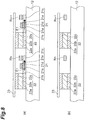
- FIG. 3 are views showing a configuration of a solid-state imaging device 10 as an example of a device for realizing the control method according to the respective embodiments to be described below.
- Fig. 1 is a plan view showing the solid-state imaging device 10
- Fig. 2 is a partially enlarged plan view of the solid-state imaging device 10.
- Fig. 3 is a side sectional view showing a section taken along a line I-I of Fig. 2 .
- an XYZ orthogonal coordinate system is also shown for easy understanding.
- the solid-state imaging device 10 includes a solid-state imaging element 11.
- the solid-state imaging element 11 is a control object in the following respective embodiments, and includes a glass substrate 12 and a photodetecting region 20 and a vertical shift register section 30 fabricated on a principal surface of the glass substrate 12.
- the vertical shift register section 30 is disposed along a lateral side of the photodetecting region 20.
- the solid-state imaging device 10 further includes a signal output section 40 disposed separately from the solid-state imaging element 11.
- the signal output section 40 is composed of, for example, a plurality of C-MOS IC chips 41 electrically connected with the photodetecting region 20.
- the signal output section 40 includes N integration circuits provided for each of the N columns of the photodetecting region 20, and these N integration circuits generate voltage values according to the amounts of charges output from the pixels of the first column through the N-th column.
- the signal output section 40 holds voltage values output from the respective integration circuits, and outputs the held voltage values successively.
- the photodetecting region 20 and the vertical shift register section 30 may be respectively provided on separate glass substrates 12. Further, the signal output section 40 may be provided on the glass substrate 12 with the photodetecting region 20 and the vertical shift register section 30.
- the photodetecting region 20 is composed of M ⁇ N pixels two-dimensionally arrayed in M rows and N columns.
- the pixel P m,n shown in Fig. 2 is a pixel located on the m-th row and the n-th column.
- m is an integer not less than 1 and not more than M
- n is an integer not less than 1 and not more than N
- M is an integer not less than 3
- N is an integer not less than 2.
- the column direction is coincident with the X-axis direction
- the row direction is coincident with the Y-axis direction.
- Each of the plurality of pixels P 1,1 to P M,N included in the photodetecting region 20 includes a transistor 21 serving as a readout switch and a photodiode 22.
- One current terminal of the transistor 21 is connected to the photodiode 22.
- the other current terminal of the transistor 21 is connected to a corresponding readout wiring line (for example, in the case of the pixel P m,n , an n-th column readout wiring line R n ).
- a control terminal of the transistor 21 is connected to a corresponding row selection wiring line (for example, in the case of the pixel P m,n , an m-th row selection wiring line Qm).
- a polycrystalline silicon film 14 is provided over the entire surface on the glass substrate 12.
- the transistor 21, the photodiode 22, and the n-th column readout wiring line R n are formed on the surface of the polycrystalline silicon film 14.
- the transistor 21, the photodiode 22, and the n-th column readout wiring line R n are covered with an insulating layer 16, and on the insulating layer 16, a scintillator 18 is provided so as to cover the entire surface of the glass substrate 12.
- the scintillator 18 generates scintillation light in response to incident X-rays to convert an X-ray image into an optical image, and outputs the optical image to the photodetecting region 20.
- the n-th column readout wiring line R n is made of metal.
- the photodiode 22 generates charge of an amount according to an incident light intensity, and accumulates the generated charge in a junction capacitance section.
- the photodiode 22 is a PIN photodiode including an n-type semiconductor layer 22a, an i-type semiconductor layer 22b, and a p-type semiconductor layer 22c.
- the n-type semiconductor layer 22a is a semiconductor layer made of n-type polycrystalline silicon.
- the i-type semiconductor layer 22b is a semiconductor layer made of i-type (undoped) amorphous silicon, and provided on the n-type semiconductor layer 22a.
- the i-type semiconductor layer 22b being formed of amorphous silicon
- the i-type semiconductor layer 22b can be made thick, so that the photoelectric conversion efficiency of the photodiode 22 can be increased to improve the sensitivity of the solid-state imaging device 10.
- the p-type semiconductor layer 22c is a semiconductor layer made of p-type amorphous silicon, and provided on the i-type semiconductor layer 22b.
- the transistor 21 is preferably constructed by a field effect transistor (FET), but may be constructed by a bipolar transistor.
- FET field effect transistor
- the control terminal means a gate
- the current terminal means a source or drain in the following description.
- the transistor 21 shown in Fig. 3 has an FET configuration, and includes a region made of polycrystalline silicon.
- the transistor 21 includes a channel region 21a, a source region 21b, and a drain region 21c, each of which is made of polycrystalline silicon.
- the source region 21b is formed along one side surface of the channel region 21a.
- the drain region 21c is formed along the other side surface of the channel region 21a.
- a gate electrode 21e on the channel region 21a, and there is interposed a gate insulating film 21d between the gate electrode 21e and the channel region 21a.
- the polycrystalline silicon that forms the channel region 21a, the source region 21b, and the drain region 21c of the transistor 21 is more preferably low-temperature polycrystalline silicon (LTPS; Low Temperature Polycrystalline Silicon).
- the low-temperature polycrystalline silicon is polycrystalline silicon that is deposited at a relatively-low process temperature of 100 to 600°C. Under such a low temperature, because a glass substrate 12 such as, for example, alkali-free glass can be used as a support substrate, setting the forming material of the above-mentioned respective regions 21a, 21b, and 21c as low-temperature polycrystalline silicon allows using as a support substrate a glass substrate 12 having a large area as compared with a monocrystalline silicon wafer to fabricate a large-area photodetecting region 20 on the glass substrate 12.
- LTPS Low Temperature Polycrystalline Silicon
- the material for the glass substrate 12 for example, sheet-like alkali-free glass (for substrate use) having a thickness such as 0.3mm to 1.2mm is used.
- the alkali-free glass contains little alkali, has a low coefficient of expansion and high heat resistance, and has stable characteristics.
- the electron mobility in low-temperature polycrystalline silicon is 10 to 600cm 2 /Vs, which is greater than the electron mobility (0.3 to 1.0cm 2 /Vs) in amorphous silicon, and therefore, forming the regions 21a, 21b, and 21c of the transistor 21 by low-temperature polycrystalline silicon allows lowering the on-resistance of the transistor 21.
- the pixel P m,n as shown in Fig. 3 is fabricated, for example, by the following process.
- As the film forming method for example, plasma CVD is favorable.
- a SiO 2 film to serve as a gate insulating film 21d is formed on a partial region of the polycrystalline silicon film 14, a gate electrode 21e is formed thereon.
- ions are implanted into respective regions to be the source region 21b and the drain region 21c. Subsequently, by carrying out patterning of the polycrystalline silicon film 14, exposure and etching are repeatedly carried out to form other electrodes and contact holes, etc. Moreover, after ions are implanted into a region to be the pixel P m,n in the polycrystalline silicon film 14 so as to become n-type, i-type and p-type amorphous silicon layers (i.e. an i-type semiconductor layer 22b and a p-type semiconductor layer 22c) are deposited thereon in order to form a PIN photodiode 22. Subsequently, a passivation film to serve as the insulating layer 16 is formed.
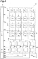
- Fig. 4 is a diagram showing an internal configuration of the solid-state imaging device 10.
- the photodetecting region 20 consists of M ⁇ N pixels P 1,1 to P M,N arrayed two-dimensionally in M rows and N columns.
- the N pixels P m,1 to P m,N of the m-th row are connected to the vertical shift register section 30 via the m-th row selection wiring line Q m .
- the vertical shift register section 30 is included in a controlling section 6.
- the signal output section 40 includes N integration circuits 42 and N holding circuits 44 provided for each column.
- the integration circuits 42 and the holding circuits 44 are connected in series with each other for each column.
- the N integration circuits 42 have a common configuration with each other.
- the N holding circuits 44 have a common configuration with each other.
- Each of the N integration circuits 42 has an input terminal connected to each of the readout wiring lines R 1 to R N , and accumulates a charge input to the input terminal from each of the readout wiring lines R 1 to R N , and outputs a voltage value according to the accumulated charge amount from an output terminal to each of the N holding circuits 44.
- Each of the N integration circuits 42 is connected to the controlling section 6 via a reset wiring line 46 provided in common for the N integration circuits 42.
- Each of the N holding circuits 44 has an input terminal connected to the output terminal of the integration circuit 42, holds a voltage value input to the input terminal, and outputs the held voltage value from an output terminal to a voltage output wiring line 48.
- Each of the N holding circuits 44 is connected to the controlling section 6 via a hold wiring line 45 provided in common for the N holding circuits 44. Moreover, each of the N holding circuits 44 is connected to a horizontal shift register section 61 of the controlling section 6 via each of the first column selection wiring line U 1 to the N-th column selection wiring line U N .
- the vertical shift register section 30 of the controlling section 6 provides an m-th row selection control signal VS m to each of the N pixels P m,1 to P m,N of the m-th row via the m-th row selection wiring line Q m .
- row selection control signals VS 1 to VS M sequentially take significant values.
- the horizontal shift register section 61 of the controlling section 6 provides column selection control signals HS 1 to HS N to the respective N holding circuits 44 via the column selection wiring lines U 1 to U N .
- the column selection control signals HS 1 to HS N sequentially take significant values.
- the controlling section 6 provides a reset control signal RE to each of the N integration circuits 42 via the reset wiring line 46, and provides a hold control signal Hd to each of the N holding circuits 44 via the hold wiring line 45.
- Fig. 5 is a diagram showing an example of a circuit configuration of each of the pixel P m,n , integration circuit 42, and holding circuit 44 of the solid-state imaging device 10.
- a circuit diagram of the pixel P m,n is shown as a representative of the M ⁇ N pixels P 1,1 to P M,N .
- the anode terminal of the photodiode 22 of the pixel P m,n is grounded, and the cathode terminal is connected to the readout wiring line R n via the transistor 21.
- the transistor 21 of the pixel P m,n is provided with an m-th row selection control signal VS m via the m-th row selection wiring line Q m from the vertical shift register section 30.
- the m-th row selection control signal VS m instructs an opening and closing operation of the transistor 21 included in each of the N pixels P m,1 to P m,N of the m-th row.
- the transistor 21 reaches a non-connected state. At this time, a charge generated in the photodiode 22 is not output to the column readout wiring line R n , but is accumulated in the junction capacitance section of the photodiode 22.
- the transistor 21 reaches a connected state. At this time, the charge that has been accumulated in the junction capacitance section of the photodiode 22 is output to the readout wiring line R n through the transistor 21. This charge is sent to the integration circuit 42 via the readout wiring line R n .
- the integration circuit 42 includes an amplifier 42a, a capacitive element 42b, and a discharge switch 42c.
- the capacitive element 42b and the discharge switch 42c are connected in parallel with each other, and connected between an input terminal and an output terminal of the amplifier 42a.
- the input terminal of the amplifier 42a is connected with the readout wiring line R n .
- the discharge switch 42c is provided with a reset control signal RE via the reset wiring line 46 from the controlling section 6.
- the reset control signal RE instructs an opening and closing operation of the discharge switch 42c in each of the N integration circuits 42.
- the discharge switch 42c closes, the capacitive element 42b is discharged, and an output voltage value of the integration circuit 42 is initialized.
- the discharge switch 42c opens, a charge input to the integration circuit 42 is accumulated in the capacitive element 42b, and a voltage value according to the accumulated charge amount is output from the integration circuit 42.
- the holding circuit 44 includes an input switch 44a, an output switch 44b, and a capacitive element 44c. One end of the capacitive element 44c is grounded. The other end of the capacitive element 44c is connected to the output terminal of the integration circuit 42 via the input switch 44a, and connected with the voltage output wiring line 48 via the output switch 44b.
- the input switch 44a is provided with a hold control signal Hd via the hold wiring line 45 from the controlling section 6.
- the hold control signal Hd instructs an opening and closing operation of the input switch 44a in each of the N holding circuits 44.
- the output switch 44b of the holding circuit 44 is provided with an n-th column selection control signal HS n passed through the n-th column selection wiring line U n from the controlling section 6.
- the selection control signal HS n instructs an opening and closing operation of the output switch 44b of the holding circuit 44.
- the input switch 44a switches from a closed state to an open state, and a voltage value being input to the holding circuit 44 at this time is held in the capacitive element 44c.
- the output switch 44b closes, and the voltage value held in the capacitive element 44c is output to the voltage output wiring line 48.
- Fig. 6 and Fig. 7 are timing charts of respective signals to be applied to the solid-state imaging element 11 in a control method for a solid-state imaging element according to a first embodiment.
- Fig. 6 shows a mode (a normal readout mode) for reading out charges from all pixels in the photodetecting region 20.
- Fig. 7 shows a mode (a partial readout mode) for reading out charges from only pixels in a partial region (an interest region) of the photodetecting region 20.
- Fig. 6 shows, in order from the top, (a) the reset control signal RE, (b) the first row selection control signal VS 1 , (c) the second row selection control signal VS 2 , (d) the third row selection control signal VS 3 , (e) the fourth row selection control signal VS 4 , (f) the fifth row selection control signal VS 5 , (g) the M-th row selection control signal VS M , (h) the hold control signal Hd, and (i) the first column selection control signal HS 1 to the N-th column selection control signal HS N , respectively.
- Fig. 6 shows, in order from the top, (a) the reset control signal RE, (b) the first row selection control signal VS 1 , (c) the second row selection control signal VS 2 , (d) the third row selection control signal VS 3 , (e) the fourth row selection control signal VS 4 , (f) the fifth row selection control signal VS 5 , (g) the M-th row selection control signal VS M
- FIG. 7 shows, in order from the top, (a) the reset control signal RE, (b) the first row selection control signal VS 1 , (c) the second row selection control signal VS 2 , (d) the third row selection control signal VS 3 , (e) the fourth row selection control signal VS 4 , (f) the fifth row selection control signal VS 5 , (g) the (mp-2)-th row selection control signal VS mp-2 , (h) the (mp-1)-th row selection control signal VS mp-1 , (i) the mp-th row selection control signal VS mp , (j) the (mp+1)-th row selection control signal VS mp+1 , (k) the M-th row selection control signal VS M , (m) the hold control signal Hd, and (n) the first column selection control signal HS 1 to the N-th column selection control signal HS N , respectively.
- the controlling section 6 makes the reset control signal RE high level. Accordingly, in each of the N integration circuits 42, the discharge switch 42c reaches a closed state, and the capacitive element 42b is discharged.
- the controlling section 6 makes the first row selection control signal VS 1 high level. Accordingly, the transistors 21 reach a connected state in the pixels P 1,1 to P 1,N of the first row, charges accumulated in the photodiodes 22 of the respective pixels P 1,1 to P 1,N are output to the integration circuits 42 through the readout wiring lines R 1 to R N , and accumulated in the capacitive elements 42b. From the integration circuits 42, voltage values of the magnitudes according to the amounts of charges accumulated in the capacitive elements 42b are output. Also, after the time t 13 , the transistor 21 in each of the pixels P 1,1 to P 1,N of the first row is brought into a non-connected state.
- the controlling section 6 makes the hold control signal Hd high level, and accordingly, the input switch 44a reaches a connected state in each of the N holding circuits 44, and a voltage value output from the integration circuit 42 is held by the capacitive element 44c.
- the controlling section 6 makes the first column selection control signal HS 1 to the N-th column selection control signal HS N sequentially high level. Accordingly, the output switches 44b of the N holding circuits 44 sequentially reach a closed state, and the voltage values that have been held in the capacitive elements 44c are successively output to the voltage output wiring line 48. Moreover, during this period, the controlling section 6 makes the reset control signal RE high level, and the capacitive element 42b of the integration circuit 42 is discharged.
- the controlling section 6 makes the second row selection control signal VS 2 high level. Accordingly, the transistors 21 reach a connected state in the pixels P 2,1 to P 2,N of the second row, charges accumulated in the photodiodes 22 of the respective pixels P 2,1 to P 2,N are output to the integration circuits 42 through the readout wiring lines R 1 to R N , and accumulated in the capacitive elements 42b. Thereafter, by the same operation as with the first row, voltage values of the magnitudes according to the amounts of charges accumulated in the capacitive elements 42b are successively output from the N holding circuits 44 to the voltage output wiring line 48.
- charges accumulated in the pixels of the third row through the M-th row are also converted into voltage values by the same operation as with the first row, and are successively output to the voltage output wiring line 48.
- readout of one imaging frame of image data from the photodetecting region 20 is completed.
- the controlling section 6 makes the reset control signal RE high level. Accordingly, in each of the N integration circuits 42, the discharge switch 42c reaches a closed state. Moreover, in this period from the time t 20 to the time t 21 , the controlling section 6 makes, of the first row to the (mp-1)-th row that are non-readout object rows, odd numbered rows, that is, the first row selection control signal VS 1 , the third row selection control signal VS 3 , ..., the (mp-2)-th row selection control signal VS mp-2 , successively high level.
- the following operation is performed successively in the odd numbered rows of the (mp-1) non-readout object rows. That is, the transistors 21 sequentially reach a connected state in the respective pixels contained in the rows, and charges accumulated in the photodiodes 22 are output to the integration circuits 42 through the readout wiring lines R 1 to R N . During this period, because the discharge switches 42c of the integration circuits 42 are always in a closed state, charges that have reached the integration circuits 42 are removed to a reference potential line (GND line). By such operation, the photodiodes 22 of the pixels contained in the odd numbered rows of the (mp-1) non-readout object rows are reset.
- GND line reference potential line
- the controlling section 6 makes the mp-th row selection control signal VS mp high level. Accordingly, the transistors 21 reach a connected state in the pixels P mp,1 to P mp,N of the mp-th row, charges accumulated in the photodiodes 22 of the respective pixels P mp,1 to P mp,N are output to the integration circuits 42 through the readout wiring lines R 1 to R N , and accumulated in the capacitive elements 42b. From the integration circuits 42, voltage values of the magnitudes according to the amounts of charges accumulated in the capacitive elements 42b are output. Also, after the time t 23 , the transistor 21 in each of the pixels P mp,1 to P mp,N of the mp-th row is brought into a non-connected state.
- the controlling section 6 makes the hold control signal Hd high level. Accordingly, a voltage value output from the integration circuit 42 is held by the capacitive element 44c.
- the controlling section 6 makes the first column selection control signal HS 1 to the N-th column selection control signal HS N sequentially high level. Accordingly, the voltage values that have been held in the capacitive elements 44c are successively output to the voltage output wiring line 48. Moreover, during this period, the controlling section 6 makes the reset control signal RE high level, and the capacitive element 42b of the integration circuit 42 is discharged.
- the controlling section 6 makes the (mp+1)-th row selection control signal VS mp+1 high level. Accordingly, the transistors 21 reach a connected state in the pixels P mp+1,1 to P mp+1,N of the (mp+1)-th row, charges accumulated in the photodiodes 22 of the respective pixels P mp+1,1 to P mp+1,N are output to the integration circuits 42 through the readout wiring lines R 1 to R N , and accumulated in the capacitive elements 42b.
- the controlling section 6 makes the reset control signal RE high level. Accordingly, in each of the N integration circuits 42, the discharge switch 42c reaches a closed state. Moreover, in this period from the time t 30 to the time t 31 , the controlling section 6 makes, of the first row to the (mp-1)-th row that are non-readout object rows, even numbered rows, that is, the second row selection control signal VS 2 , the fourth row selection control signal VS 4 , ..., the (mp-1)-th row selection control signal VS mp-1 , successively high level.
- the photodiodes 22 are reset successively in the even numbered rows of the (mp-1) non-readout object rows. Thereafter, the above-described operation from the time t 21 to the time t 29 is repeated again. Thus, readout of the next one frame of image data from the readout object rows of the photodetecting region 20 is completed.
- Fig. 8 includes views for explaining an overflow state.
- (a) in Fig. 8 is a schematic view showing a section of the photodetecting region 20 cut along a cutting plane including transistors 21.
- (b) in Fig. 8 is a schematic view showing a section of the photodetecting region 20 cut along a cutting plane not including transistors 21.
- the p-type semiconductor layer 22c is connected to a transparent reference potential line (GND line) 23. Therefore, it is considered that, when charge is excessively accumulated in the photodiode 22, the potential of the reference potential line 23 varies locally via the p-type semiconductor layer 22c. Also, because the reference potential line 23 has a significant resistance value, it is considered that such a potential variation occurs only in the vicinity of the pixel concerned.
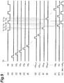
- FIG. 9 is a timing chart showing an example of a control method for a solid-state imaging element, including a process for resetting charges of the photodiodes 22 included in non-readout object rows. Also, in Fig. 9 , the respective signals shown in (a) to (n) are the same as those of Fig. 7 in the foregoing.
- the controlling section makes the first row selection control signal VS 1 , the second row selection control signal VS 2 , ..., the (mp-1)-th row selection control signal VS mp-1 corresponding to the first row to the (mp-1)-th row that are non-readout object rows successively high level. Accordingly, in all of the (mp-1) non-readout object rows, the photodiodes 22 are successively reset. Thereafter, by similarly performing the operation from the time t 22 to the time t 29 shown in Fig. 7 , readout of one imaging frame of image data from the readout object rows of the photodetecting region 20 is completed.
- the solid-state imaging element 11 For control of the solid-state imaging element 11, it is demanded to reduce the time required per one imaging frame (frame rate) as much as possible.
- the photodiodes 22 of all non-readout object rows are sequentially reset in one imaging frame, there is a problem that the required time for the respective imaging frames is prolonged.
- the larger the area of the photodetecting region 20 and the larger the number of pixels to compose the photodetecting region 20 the longer time is required for resetting the photodiodes 22 of the non-readout object rows, and the required time for imaging frames is further prolonged.
- a removing processing is performed for only a part of the two or more non-readout object rows (the first row to the (mp-1)-th row) in each of the two times of imaging frames.
- resetting of charges accumulated in pixels contained in the odd numbered non-readout object rows (the first row, the third row, ..., the (mp-2)-th row) is performed in one imaging frame, and resetting of charges accumulated in pixels contained in the even numbered non-readout object rows (the second row, the fourth row, ..., the (mp-1)-th row) is performed in the next imaging frame.
- resetting of charges accumulated in pixels is always performed at least once in the period of two times of imaging frames for each of the two or more non-readout object rows.
- resetting of charges accumulated in the pixels contained in non-readout object rows is preferably successively performed.
- the control method according to the present embodiment even when resetting of non-readout object rows is successively performed, the time required per one imaging frame can be reduced. And, by successively performing resetting of non-readout object rows, current that flows to the wiring line can be further reduced, and load on the peripheral circuit such as a power supply can be remarkably reduced.
- the non-readout object rows (the first row, the third row, ..., and the (mp-2)-th row, or the second row, the fourth row, ..., and the (mp-1)-th row) to be reset in one imaging frame are disposed at intervals of one row from each other.
- the non-readout object rows are preferably spaced from each other at intervals of one or more rows. Accordingly, the positions of non-readout object rows where resetting is performed in the respective imaging frames can be dispersed, and a charge overflow to the readout object rows (the mp-th row to the M-th row) can be more effectively suppressed.
- the channel region 21a, the source region 21b, and the drain region 21c of the transistor 21 are made of polycrystalline silicon.
- solid-state imaging elements such as two-dimensional flat panel image sensors to be used, for example, for medical purposes (such as dental radiography)
- wider photodetecting surfaces have been demanded.
- photodetecting sections are fabricated on monocrystalline silicon wafers as in prior solid-state imaging elements, the extent of photodetecting surfaces of the solid-state imaging elements is limited due to the size of the monocrystalline silicon wafers that are at most 12 inches in diameter.
- forming a film of polycrystalline silicon on an insulating substrate such as a glass substrate, and forming photodiodes and other electronic components such as transistors on the surface of the polycrystalline silicon enables making the photodetecting surfaces remarkably wide as compared with those of conventional solid-state imaging elements formed with use of monocrystalline silicon wafers.
- the channel region 21a, the source region 21b, and the drain region 21c of the transistor 21 may be made of amorphous silicon, and may be made both of polycrystalline silicon and amorphous silicon. Also in this case, the effects described above can be favorably obtained.
- the transistor 21 made of amorphous silicon has a problem (a so-called memory effect) that a charge is transiently trapped when the transistor is brought into a non-connected state. This is because amorphous silicon is non-crystalline, and therefore results in a high density of levels to trap a charge in FET channels.
- polycrystalline silicon particularly, low-temperature polycrystalline silicon
- forming the transistor 21 by polycrystalline silicon allows suppressing the occurrence of such a memory effect.
- Fig. 10 is a timing chart of respective signals to be applied to the solid-state imaging element 11 in the control method for a solid-state imaging element according to the second embodiment, and shows a mode (a partial readout mode) for reading out charges from only pixels in a partial region (an interest region) of the photodetecting region 20.
- a mode a partial readout mode for reading out charges from only pixels in a partial region (an interest region) of the photodetecting region 20.
- the controlling section 6 makes the reset control signal RE high level. Accordingly, in each of the N integration circuits 42, the discharge switch 42c reaches a closed state. And, in this period from the time t 20 to the time t 21 , the controlling section 6 makes, of the first row through the (mp-1)-th row that are non-readout object rows, odd numbered rows, that is, the first row selection control signal VS 1 , the third row selection control signal VS 3 , ..., the (mp-2)-th row selection control signal VS mp-2 , high level.
- the timing to make these row selection control signals VS 1 , VS 3 , ..., VS mp-2 high level is different from that of the first embodiment.
- These row selection control signals VS 1 , VS 3 , ..., VS mp-2 were made high level sequentially in the first embodiment, while in the present embodiment, these row selection control signals VS 1 , VS 3 , ..., VS mp-2 are made high level simultaneously.
- the following operation is performed simultaneously in the odd numbered rows of the (mp-1) non-readout object rows. That is, the transistors 21 all together reach a connected state in the respective pixels contained in these rows, and charges accumulated in the photodiodes 22 are output to the integration circuits 42 through the readout wiring lines R 1 to R N . During this period, because the discharge switches 42c of the integration circuits 42 are always in a closed state, charges that have reached the integration circuits 42 are removed to a reference potential line (GND line). By such operation, the photodiodes 22 of the pixels contained in the odd numbered rows of the (mp-1) non-readout object rows are reset.
- GND line reference potential line
- the controlling section 6 makes the reset control signal RE high level. Accordingly, in each of the N integration circuits 42, the discharge switch 42c reaches a closed state. And, in this period from the time t 30 to the time t 31 , the controlling section 6 makes, of the first row through the (mp-1)-th row that are non-readout object rows, even numbered rows, that is, the second row selection control signal VS 2 , the fourth row selection control signal VS 4 , ..., the (mp-1)-th row selection control signal VS mp-1 , high level.
- these row selection control signals VS 2 , VS 4 , ..., VS mp-1 are made high level simultaneously. Accordingly, the photodiodes 22 are reset simultaneously in the even numbered rows of the (mp-1) non-readout object rows. Thereafter, the above-described operation from the time t 21 to the time t 29 is repeated again. Thus, readout of the next imaging frame of image data from the readout object rows of the photodetecting region 20 is completed.
- Fig. 11 is a timing chart showing a comparative example of a control method for a solid-state imaging element.
- the controlling section makes the first row selection control signal VS 1 , the second row selection control signal VS 2 , ..., the (mp-1)-th row selection control signal VS mp-1 corresponding to the first row through the (mp-1)-th row that are non-readout object rows simultaneously high level.
- the photodiodes 22 are simultaneously reset. Thereafter, by similarly performing the operation from the time t 22 to the time t 29 shown in Fig. 10 , readout of one imaging frame of image data from the readout object rows of the photodetecting region 20 is completed.
- the row selection control signals VS 1 through VS mp-1 corresponding to all non-readout object rows are output all together from the vertical shift register section 30, when the current supply capacity of the power supply is not sufficient, the rising time of the row selection control signals VS 1 through VS mp-1 is prolonged.
- a power supply circuit having a sufficient capacity and integration circuits 42 the output impedance of which is sufficiently small are required, which contributes to an increase in manufacturing cost.
- one time of removing processing is secured in the period of two times of imaging frames for each of the two or more non-readout object rows (the first row to the (mp-1)-th row), while in the respective imaging frames, resetting of charges accumulated in pixels contained in only a part of the non-readout object rows is performed. Accordingly, current that flows inside of the vertical shift register section 30 and to the readout wiring lines R 1 to R N can be reduced, and load on the peripheral circuit such as a power supply can be reduced.
- resetting of charges accumulated in pixels contained in non-readout object rows may be simultaneously performed.
- load on the peripheral circuit can be reduced.
- simultaneously performing resetting of non-readout object rows the required time for the respective imaging frames can be further reduced.
- the non-readout object rows (the first row, the third row, ..., and the (mp-2)-th row, or the second row, the fourth row, ..., and the (mp-1)-th row) to be reset in one imaging frame are disposed at intervals of one row from each other.
- the non-readout object rows are preferably spaced from each other at intervals of one or more rows. Accordingly, the positions of non-readout object rows where resetting is performed in the respective imaging frames can be dispersed, and a charge overflow to the readout object rows (the mp-th row to the M-th row) can be more effectively suppressed.
- FIG. 12 includes views schematically showing a state of resetting non-readout object rows in such a control method.
- Each of (a) to (d) in Fig. 12 shows each of the four consecutive imaging frames, and in each figure, an interest region A1 consisting of one or two or more readout object rows, a non-interest region A2 consisting of two or more non-readout object rows, and non-readout object rows A3 to serve as reset objects in the respective imaging frames are shown.
- the odd-numbered non-readout object rows A3 are reset in the first imaging frame ((a) in Fig. 12 ) and the third imaging frame ((c) in Fig. 12 ), and the even-numbered non-readout object rows A3 are reset in the second imaging frame ((b) in Fig. 12 ) and the fourth imaging frame ((d) in Fig. 12 ).
- Fig. 13 includes schematic views showing a second example of a reset object row arrangement in respective imaging frames.
- a plurality of rows contained in the non-interest region A2 are divided into row groups of four rows each, and resetting of one row per one frame is performed successively for each row group.
- Fig. 14 includes schematic views showing a third example of a reset object row arrangement in respective imaging frames.
- a plurality of rows contained in the non-interest region A2 are divided into row groups of three rows each, and one row group per one frame is successively reset.
- reset object rows are arranged for example as in these, the same effects as those of the above-described respective embodiments can be favorably obtained.
- Fig. 15 includes schematic views showing a fourth example of a reset object row arrangement in respective imaging frames.
- a plurality of rows contained in the non-interest region A2 are divided into four row groups A21 to A24.
- the row group A21 consists of one non-readout object row
- the row group A22 consists of two non-readout object rows
- the row group A23 consists of four non-readout object rows
- the row group A24 consists of eight non-readout object rows.
- resetting is performed for all non-readout object row A3 for every imaging frame.
- resetting of the respective non-readout object row is performed four times in the period of four imaging frames.
- one non-readout object row A3 is reset in the first imaging frame ((a) in Fig. 15 ) and the third imaging frame ((c) in Fig. 15 )
- the other non-readout object row A3 is reset in the second imaging frame ((b) in Fig. 15 ) and the fourth imaging frame ((d) in Fig. 15 ). That is, in the row group A22, resetting is performed two times for each non-readout object row in the period of four imaging frames.
- one non-readout object row A3 is reset in each of the first imaging frame ((a) in Fig. 15 ) through the fourth imaging frame ((d) in Fig. 15 ). That is, in the row group A23, resetting is performed once for each non-readout object row in the period of four imaging frames.
- one non-readout object row A3 is reset in each of the first imaging frame ((a) in Fig. 15 ) through the eighth imaging frame (not shown). That is, in the row group A24, resetting is performed once for each non-readout object row in the period of eight imaging frames.
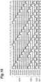
- Fig. 16 is a timing chart showing a control method for realizing the reset object row arrangement shown in Fig. 15 .
- Fig. 16 shows a resetting operation for each of the non-readout object rows (the first row through the fifteenth row), and for each of the imaging frames (the first imaging frame to the twenty-fourth imaging frame are shown in the figure), it is shown as high level in the imaging frame where resetting is performed, and shown as low level in the imaging frame where resetting is not performed.
- the frequency of resetting of the row group A21 adjacent to the interest region A1 is greater than the frequency of resetting of the other row groups. Further, it is preferable that the closer to the interest region A1, the greater the frequency of resetting of the non-readout object row, and the farther from the interest region A1, the smaller the frequency of resetting of the non-readout object row. Accordingly, the influence on the readout object rows (interest region A1) due to a charge overflow and the like in the non-readout object rows can be more effectively suppressed, and charges accumulated in the respective pixels of the readout object rows (interest region A1) can be more accurately read out.
- Fig. 17 includes schematic views showing a fifth example of a reset object row arrangement in respective imaging frames.
- a plurality of rows contained in the non-interest region A2 are divided into four row groups A21 to A23 and A25.
- the row group A21 consists of one non-readout object row
- the row group A22 consists of two non-readout object rows
- the row group A23 consists of four non-readout object rows
- the row group A25 consists of eight non-readout object rows.
- resetting of the respective non-readout object rows is performed in the same manner as with the foregoing fourth example.
- the row group A25 resetting is not performed at all.
- Fig. 18 is a timing chart showing a control method for realizing the reset object row arrangement shown in Fig. 17 .
- Fig. 18 shows a resetting operation for each of the non-readout object rows (the first row through the fifteenth row), and for each of the imaging frames (the first imaging frame to the twenty-fourth imaging frame are shown in the figure), it is shown as high level in the imaging frame where resetting is performed, and shown as low level in the imaging frame where resetting is not performed.
- the row group for which resetting is not performed is the row group A25 farthest from the interest region A1.
- control method for a solid-state imaging element by the present invention is not limited to the respective embodiments and modifications described above, and various other modifications can be made.
- Fig. 19 includes views for explaining an overflow state at partial readout time when a photodetecting region is formed on a p-type monocrystalline silicon substrate 70.
- the photodetecting region formed on the p-type monocrystalline silicon substrate 70 has photodiodes 24 in the respective pixels in place of the photodiodes 22 shown in Fig. 2 .
- (a) in Fig. 19 is a schematic view showing a section that is obtained by cutting the photodiodes 24 at a cutting plane including transistors 21, and
- (b) in Fig. 19 is a schematic view showing a section that is obtained by cutting the photodiodes 24 at a cutting plane not including transistors 21.
- FIG. 19 includes views for explaining an overflow state at partial readout time when a photodetecting region is formed on a p-type monocrystalline silicon substrate 70.
- the photodetecting region formed on the p-type monocrystalline silicon substrate 70 has photodiodes 24 in the respective pixels in place of the photodiodes 22 shown in Fig. 2 .
- the photodiode 24 includes an n + -type semiconductor region 24a formed by ion implantation or the like for the p-type monocrystalline silicon substrate 70. Further, the n + -type semiconductor region 24a is surrounded by a p + -type semiconductor region 24b formed by ion implantation or the like for the p-type monocrystalline silicon substrate 70.
- an FET has been exemplified as the transistor 21 included in each pixel in the above-described embodiments and respective modifications, but the transistor 21 may be a bipolar transistor.
- the control terminal means a base and the current terminal means a collector or an emitter.
- at least one time of removing processing is performed in the period of two times of imaging frames, and in the above-mentioned respective modifications, at least one time of removing processing is performed in the period of at most of eight times of imaging frames.
- the number of imaging frames for removing processing is not limited to these, and by performing at least one time of removing processing in the period of an arbitrary number of L times (L is an integer not less than 2) of imaging frames, the effects described in the respective embodiments can be favorably provided.
- the present invention can be applied as a control method for a solid-state imaging element capable of reducing the time required per one imaging frame and reducing load on the peripheral circuit when selectively reading out charges accumulated in pixels in a partial region of the photodetecting region.
Landscapes
- Engineering & Computer Science (AREA)
- Multimedia (AREA)
- Signal Processing (AREA)
- Transforming Light Signals Into Electric Signals (AREA)
- Solid State Image Pick-Up Elements (AREA)
- Health & Medical Sciences (AREA)
- Toxicology (AREA)
- Chemical & Material Sciences (AREA)
- Materials Engineering (AREA)
- Nanotechnology (AREA)
Claims (10)
- Procédé de commande pour un élément d'imagerie à semi-conducteurs (11) incluant une région de photodétection (20) présentant MxN, M est un entier de pas moins de 3, N est un entier de pas moins de 2, pixels incluant chacun une photodiode (22) et un commutateur d'extraction (21) connecté à une extrémité à la photodiode (22) qui sont disposés en mode bidimensionnel en M rangées et N colonnes, le procédé incluant les étapes consistant à
sélectionner une ou une pluralité de rangées d'objets d'extraction (A1) formant une région partielle de la région de photodétection en fournissant un signal de commande de sélection,
extraire, dans L trames d'imagerie, dans lequel L est un entier de pas moins de 2, des charges accumulées dans les pixels contenus dans la une ou la pluralité sélectionnée de rangées d'objets d'extraction (A1),
pour chaque trame d'imagerie, effectuer un traitement de retrait de charges accumulées dans les pixels contenus dans seulement une partie de deux rangées ou plus (A21, A22, A23) incluses dans des rangées d'objets de non-extraction (A2),
caractérisé en ce que
le traitement de retrait est effectué au moins une fois dans une période couvrant les L trames d'imagerie pour chacun des pixels des rangées d'objets de non-extraction (A2). - Procédé de commande pour un élément d'imagerie à semi-conducteurs (11) selon la revendication 1, dans lequel une fréquence du traitement de retrait pour une ou une pluralité de rangées incluses dans les rangées d'objets de non-extraction et adjacentes aux rangées d'objets d'extraction est supérieure à une fréquence du traitement de retrait pour le reste des rangées d'objets de non-extraction.
- Procédé de commande pour un élément d'imagerie à semi-conducteurs (11) selon la revendication 1 ou 2, dans lequel, dans chacune des L trames d'imagerie, un traitement de retrait de charges accumulées dans les pixels contenus dans la partie des deux rangées ou plus est simultanément effectué.
- Procédé de commande pour un élément d'imagerie à semi-conducteurs (11) selon la revendication 1 ou 2, dans lequel, dans chacune des L trames d'imagerie, un traitement de retrait de charges accumulées dans les pixels contenus dans la partie des deux rangées ou plus est successivement effectué.
- Procédé de commande pour un élément d'imagerie à semi-conducteurs (11) selon l'une quelconque des revendications 1 à 4, dans chacune des L trames d'imagerie, les rangées de la partie des deux rangées ou plus pour lesquelles le traitement de retrait est effectué sont espacées l'une de l'autre avec un intervalle d'une ou plusieurs rangées.
- Procédé de commande pour un élément d'imagerie à semi-conducteurs (11) selon l'une quelconque des revendications 1 à 5, dans lequel, dans les L trames d'imagerie, un traitement de retrait de charges accumulées dans les pixels contenus dans d'autres rangées que la partie de deux rangées ou plus dans les rangées d'objets de non-extraction n'est pas effectué.
- Dispositif d'imagerie à semi-conducteurs (10) comprenant :un élément d'imagerie à semi-conducteurs (11) incluant une région de photodétection (20) présentant MxN, M est un entier de pas moins de 3, N est un entier de pas moins de 2, pixels incluant chacun une photodiode (22) et un commutateur d'extraction (21) connecté à une extrémité à la photodiode (22) qui sont disposés en mode bidimensionnel en M rangées et N colonnes ; etune section de commande (6) configurée pour commander l'élément d'imagerie à semi-conducteurs (11) et configurée en outre poursélectionner une ou une pluralité de rangées d'objets d'extraction (A1) formant une région partielle de la région de photodétection en fournissant un signal de commande de sélection,extraire, dans L trames d'imagerie, dans lequel L est un entier de pas moins de 2, des charges accumulées dans les pixels contenus dans la une ou la pluralité sélectionnée de rangées d'objets d'extraction (A1),pour chaque trame d'imagerie, effectuer un traitement de retrait de charges accumulées dans les pixels contenus dans seulement une partie de deux rangées ou plus (A21, A22, A23) incluses dans des rangées d'objets de non-extraction (A2),caractérisé en ce quele traitement de retrait est effectué au moins une fois dans une période couvrant les L trames d'imagerie pour chacun des pixels des rangées d'objets de non-extraction (A2).
- Dispositif d'imagerie à semi-conducteurs (10) selon la revendication 7,
dans lequel l'élément d'imagerie à semi-conducteurs (11) inclut une couche de semi-conducteurs faite de silicium polycristallin. - Dispositif d'imagerie à semi-conducteurs (10) selon la revendication 7, dans lequel l'élément d'imagerie à semi-conducteurs (11) inclut une couche de semi-conducteurs faite de silicium amorphe.
- Dispositif d'imagerie à semi-conducteurs (10) selon la revendication 7, dans lequel l'élément d'imagerie à semi-conducteurs (11) inclut un semi-conducteur fait de silicium monocristallin.
Applications Claiming Priority (4)
| Application Number | Priority Date | Filing Date | Title |
|---|---|---|---|
| JP2011019988 | 2011-02-01 | ||
| JP2011123574A JP5714982B2 (ja) | 2011-02-01 | 2011-06-01 | 固体撮像素子の制御方法 |
| PCT/JP2011/078954 WO2012105129A1 (fr) | 2011-02-01 | 2011-12-14 | Procédé permettant de commander un dispositif de capture d'image à semi-conducteurs |
| EP11857771.7A EP2672700B1 (fr) | 2011-02-01 | 2011-12-14 | Procédé permettant de commander un dispositif de capture d'image à semi-conducteurs |
Related Parent Applications (1)
| Application Number | Title | Priority Date | Filing Date |
|---|---|---|---|
| EP11857771.7A Division EP2672700B1 (fr) | 2011-02-01 | 2011-12-14 | Procédé permettant de commander un dispositif de capture d'image à semi-conducteurs |
Publications (2)
| Publication Number | Publication Date |
|---|---|
| EP3386187A1 EP3386187A1 (fr) | 2018-10-10 |
| EP3386187B1 true EP3386187B1 (fr) | 2021-01-20 |
Family
ID=46602359
Family Applications (2)
| Application Number | Title | Priority Date | Filing Date |
|---|---|---|---|
| EP18174796.5A Active EP3386187B1 (fr) | 2011-02-01 | 2011-12-14 | Procédé de commande de dispositif de capture d'images à l'état solide |
| EP11857771.7A Active EP2672700B1 (fr) | 2011-02-01 | 2011-12-14 | Procédé permettant de commander un dispositif de capture d'image à semi-conducteurs |
Family Applications After (1)
| Application Number | Title | Priority Date | Filing Date |
|---|---|---|---|
| EP11857771.7A Active EP2672700B1 (fr) | 2011-02-01 | 2011-12-14 | Procédé permettant de commander un dispositif de capture d'image à semi-conducteurs |
Country Status (6)
| Country | Link |
|---|---|
| US (1) | US9197826B2 (fr) |
| EP (2) | EP3386187B1 (fr) |
| JP (1) | JP5714982B2 (fr) |
| KR (1) | KR101928115B1 (fr) |
| CN (1) | CN103339928B (fr) |
| WO (1) | WO2012105129A1 (fr) |
Families Citing this family (11)
| Publication number | Priority date | Publication date | Assignee | Title |
|---|---|---|---|---|
| JPH062380B2 (ja) | 1988-05-20 | 1994-01-12 | 本州製紙株式会社 | 学習計測による段ボール生産プロセスのロット替え制御方法 |
| JP5730030B2 (ja) * | 2011-01-17 | 2015-06-03 | 浜松ホトニクス株式会社 | 固体撮像装置 |
| JP6195728B2 (ja) | 2013-04-30 | 2017-09-13 | 富士フイルム株式会社 | 固体撮像素子および撮像装置 |
| FR3006500B1 (fr) * | 2013-06-04 | 2016-10-28 | Centre Nat De La Rech Scient - Cnrs - | Capteur cmos a photosites standard |
| JP6134979B2 (ja) * | 2013-06-04 | 2017-05-31 | 富士フイルム株式会社 | 固体撮像素子および撮像装置 |
| JP6184761B2 (ja) * | 2013-06-11 | 2017-08-23 | 浜松ホトニクス株式会社 | 固体撮像装置 |
| US9297998B2 (en) * | 2014-03-28 | 2016-03-29 | Amazon Technologies, Inc. | Electrode of an electrowetting device |
| JP6664122B2 (ja) * | 2014-08-20 | 2020-03-13 | パナソニックIpマネジメント株式会社 | 固体撮像装置及びカメラ |
| JP2017143092A (ja) * | 2016-02-08 | 2017-08-17 | ソニー株式会社 | ガラスインタポーザモジュール、撮像装置、および電子機器 |
| US10438332B2 (en) * | 2017-05-18 | 2019-10-08 | Semiconductor Components Industries, Llc | Methods and apparatus for selective pixel readout for image transformation |
| CN109037250B (zh) * | 2017-06-12 | 2021-11-05 | 上海耕岩智能科技有限公司 | 一种影像侦测显示装置、器件及其制备方法 |
Citations (1)
| Publication number | Priority date | Publication date | Assignee | Title |
|---|---|---|---|---|
| JP2005184358A (ja) * | 2003-12-18 | 2005-07-07 | Sony Corp | 固体撮像装置、及び画素信号読み出し方法 |
Family Cites Families (9)
| Publication number | Priority date | Publication date | Assignee | Title |
|---|---|---|---|---|
| JP3897389B2 (ja) * | 1996-02-22 | 2007-03-22 | キヤノン株式会社 | 光電変換装置の駆動方法及び光電変換装置 |
| JPH11318877A (ja) | 1998-01-29 | 1999-11-24 | Toshiba Corp | X線平面検出器を用いたx線診断装置及びx線診断装置の制御方法 |
| JP2005184777A (ja) * | 2003-11-28 | 2005-07-07 | Sanyo Electric Co Ltd | スミア演算回路、撮像装置、及び固体撮像素子の駆動方法 |
| JP2007158741A (ja) * | 2005-12-06 | 2007-06-21 | Olympus Corp | 固体撮像装置 |
| US8289430B2 (en) * | 2007-02-09 | 2012-10-16 | Gentex Corporation | High dynamic range imaging device |
| JP5101946B2 (ja) * | 2007-08-03 | 2012-12-19 | キヤノン株式会社 | 撮像装置及び撮像システム |
| JP5053869B2 (ja) * | 2008-01-10 | 2012-10-24 | キヤノン株式会社 | 固体撮像装置、撮像システム、及び固体撮像装置の駆動方法 |
| JP5272630B2 (ja) | 2008-10-03 | 2013-08-28 | ソニー株式会社 | 固体撮像素子およびその駆動方法、並びにカメラシステム |
| JP5284132B2 (ja) * | 2009-02-06 | 2013-09-11 | キヤノン株式会社 | 固体撮像装置、撮像システム、および撮像装置の駆動方法 |
-
2011
- 2011-06-01 JP JP2011123574A patent/JP5714982B2/ja active Active
- 2011-12-14 EP EP18174796.5A patent/EP3386187B1/fr active Active
- 2011-12-14 CN CN201180066659.1A patent/CN103339928B/zh active Active
- 2011-12-14 KR KR1020137022308A patent/KR101928115B1/ko active Active
- 2011-12-14 US US13/982,527 patent/US9197826B2/en active Active
- 2011-12-14 WO PCT/JP2011/078954 patent/WO2012105129A1/fr not_active Ceased
- 2011-12-14 EP EP11857771.7A patent/EP2672700B1/fr active Active
Patent Citations (1)
| Publication number | Priority date | Publication date | Assignee | Title |
|---|---|---|---|---|
| JP2005184358A (ja) * | 2003-12-18 | 2005-07-07 | Sony Corp | 固体撮像装置、及び画素信号読み出し方法 |
Also Published As
| Publication number | Publication date |
|---|---|
| CN103339928A (zh) | 2013-10-02 |
| EP2672700A4 (fr) | 2017-01-18 |
| EP2672700B1 (fr) | 2018-06-13 |
| EP2672700A1 (fr) | 2013-12-11 |
| EP3386187A1 (fr) | 2018-10-10 |
| KR20140006912A (ko) | 2014-01-16 |
| KR101928115B1 (ko) | 2018-12-11 |
| JP5714982B2 (ja) | 2015-05-07 |
| JP2012178812A (ja) | 2012-09-13 |
| WO2012105129A1 (fr) | 2012-08-09 |
| US20130308030A1 (en) | 2013-11-21 |
| CN103339928B (zh) | 2016-10-19 |
| US9197826B2 (en) | 2015-11-24 |
Similar Documents
| Publication | Publication Date | Title |
|---|---|---|
| EP3386187B1 (fr) | Procédé de commande de dispositif de capture d'images à l'état solide | |
| US9369643B2 (en) | Solid-state imaging device | |
| EP2667591B1 (fr) | Dispositif d'imagerie à semi-conducteur | |
| EP2667590B1 (fr) | Dispositif d'imagerie à semi-conducteurs et procédé d'excitation d'un dispositif d'imagerie à semi-conducteurs | |
| US9225924B2 (en) | Solid-state imaging device including signal connecting section and solid-state imaging device driving method | |
| JP5749873B1 (ja) | 固体撮像素子の制御方法 |
Legal Events
| Date | Code | Title | Description |
|---|---|---|---|
| PUAI | Public reference made under article 153(3) epc to a published international application that has entered the european phase |
Free format text: ORIGINAL CODE: 0009012 |
|
| STAA | Information on the status of an ep patent application or granted ep patent |
Free format text: STATUS: REQUEST FOR EXAMINATION WAS MADE |
|
| 17P | Request for examination filed |
Effective date: 20180529 |
|
| AC | Divisional application: reference to earlier application |
Ref document number: 2672700 Country of ref document: EP Kind code of ref document: P |
|
| AK | Designated contracting states |
Kind code of ref document: A1 Designated state(s): AL AT BE BG CH CY CZ DE DK EE ES FI FR GB GR HR HU IE IS IT LI LT LU LV MC MK MT NL NO PL PT RO RS SE SI SK SM TR |
|
| STAA | Information on the status of an ep patent application or granted ep patent |
Free format text: STATUS: EXAMINATION IS IN PROGRESS |
|
| 17Q | First examination report despatched |
Effective date: 20190814 |
|
| REG | Reference to a national code |
Ref country code: DE Ref legal event code: R079 Ref document number: 602011070039 Country of ref document: DE Free format text: PREVIOUS MAIN CLASS: H04N0005363000 Ipc: H04N0005359000 |
|
| RIC1 | Information provided on ipc code assigned before grant |
Ipc: H04N 5/359 20110101AFI20200511BHEP |
|
| GRAP | Despatch of communication of intention to grant a patent |
Free format text: ORIGINAL CODE: EPIDOSNIGR1 |
|
| STAA | Information on the status of an ep patent application or granted ep patent |
Free format text: STATUS: GRANT OF PATENT IS INTENDED |
|
| INTG | Intention to grant announced |
Effective date: 20200721 |
|
| GRAJ | Information related to disapproval of communication of intention to grant by the applicant or resumption of examination proceedings by the epo deleted |
Free format text: ORIGINAL CODE: EPIDOSDIGR1 |
|
| STAA | Information on the status of an ep patent application or granted ep patent |
Free format text: STATUS: EXAMINATION IS IN PROGRESS |
|
| GRAP | Despatch of communication of intention to grant a patent |
Free format text: ORIGINAL CODE: EPIDOSNIGR1 |
|
| STAA | Information on the status of an ep patent application or granted ep patent |
Free format text: STATUS: GRANT OF PATENT IS INTENDED |
|
| INTC | Intention to grant announced (deleted) | ||
| INTG | Intention to grant announced |
Effective date: 20201023 |
|
| GRAS | Grant fee paid |
Free format text: ORIGINAL CODE: EPIDOSNIGR3 |
|
| GRAA | (expected) grant |
Free format text: ORIGINAL CODE: 0009210 |
|
| STAA | Information on the status of an ep patent application or granted ep patent |
Free format text: STATUS: THE PATENT HAS BEEN GRANTED |
|
| AC | Divisional application: reference to earlier application |
Ref document number: 2672700 Country of ref document: EP Kind code of ref document: P |
|
| AK | Designated contracting states |
Kind code of ref document: B1 Designated state(s): AL AT BE BG CH CY CZ DE DK EE ES FI FR GB GR HR HU IE IS IT LI LT LU LV MC MK MT NL NO PL PT RO RS SE SI SK SM TR |
|
| REG | Reference to a national code |
Ref country code: GB Ref legal event code: FG4D |
|
| REG | Reference to a national code |
Ref country code: CH Ref legal event code: EP |
|
| REG | Reference to a national code |
Ref country code: AT Ref legal event code: REF Ref document number: 1357361 Country of ref document: AT Kind code of ref document: T Effective date: 20210215 |
|
| REG | Reference to a national code |
Ref country code: IE Ref legal event code: FG4D |
|
| REG | Reference to a national code |
Ref country code: DE Ref legal event code: R096 Ref document number: 602011070039 Country of ref document: DE |
|
| REG | Reference to a national code |
Ref country code: CH Ref legal event code: NV Representative=s name: SERVOPATENT GMBH, CH |
|
| REG | Reference to a national code |
Ref country code: FI Ref legal event code: FGE |
|
| REG | Reference to a national code |
Ref country code: NL Ref legal event code: MP Effective date: 20210120 |
|
| REG | Reference to a national code |
Ref country code: LT Ref legal event code: MG9D |
|
| REG | Reference to a national code |
Ref country code: AT Ref legal event code: MK05 Ref document number: 1357361 Country of ref document: AT Kind code of ref document: T Effective date: 20210120 |
|
| PG25 | Lapsed in a contracting state [announced via postgrant information from national office to epo] |
Ref country code: PT Free format text: LAPSE BECAUSE OF FAILURE TO SUBMIT A TRANSLATION OF THE DESCRIPTION OR TO PAY THE FEE WITHIN THE PRESCRIBED TIME-LIMIT Effective date: 20210520 Ref country code: NO Free format text: LAPSE BECAUSE OF FAILURE TO SUBMIT A TRANSLATION OF THE DESCRIPTION OR TO PAY THE FEE WITHIN THE PRESCRIBED TIME-LIMIT Effective date: 20210420 Ref country code: LT Free format text: LAPSE BECAUSE OF FAILURE TO SUBMIT A TRANSLATION OF THE DESCRIPTION OR TO PAY THE FEE WITHIN THE PRESCRIBED TIME-LIMIT Effective date: 20210120 Ref country code: BG Free format text: LAPSE BECAUSE OF FAILURE TO SUBMIT A TRANSLATION OF THE DESCRIPTION OR TO PAY THE FEE WITHIN THE PRESCRIBED TIME-LIMIT Effective date: 20210420 Ref country code: HR Free format text: LAPSE BECAUSE OF FAILURE TO SUBMIT A TRANSLATION OF THE DESCRIPTION OR TO PAY THE FEE WITHIN THE PRESCRIBED TIME-LIMIT Effective date: 20210120 Ref country code: GR Free format text: LAPSE BECAUSE OF FAILURE TO SUBMIT A TRANSLATION OF THE DESCRIPTION OR TO PAY THE FEE WITHIN THE PRESCRIBED TIME-LIMIT Effective date: 20210421 |
|
| PG25 | Lapsed in a contracting state [announced via postgrant information from national office to epo] |
Ref country code: SE Free format text: LAPSE BECAUSE OF FAILURE TO SUBMIT A TRANSLATION OF THE DESCRIPTION OR TO PAY THE FEE WITHIN THE PRESCRIBED TIME-LIMIT Effective date: 20210120 Ref country code: AT Free format text: LAPSE BECAUSE OF FAILURE TO SUBMIT A TRANSLATION OF THE DESCRIPTION OR TO PAY THE FEE WITHIN THE PRESCRIBED TIME-LIMIT Effective date: 20210120 Ref country code: PL Free format text: LAPSE BECAUSE OF FAILURE TO SUBMIT A TRANSLATION OF THE DESCRIPTION OR TO PAY THE FEE WITHIN THE PRESCRIBED TIME-LIMIT Effective date: 20210120 Ref country code: LV Free format text: LAPSE BECAUSE OF FAILURE TO SUBMIT A TRANSLATION OF THE DESCRIPTION OR TO PAY THE FEE WITHIN THE PRESCRIBED TIME-LIMIT Effective date: 20210120 Ref country code: RS Free format text: LAPSE BECAUSE OF FAILURE TO SUBMIT A TRANSLATION OF THE DESCRIPTION OR TO PAY THE FEE WITHIN THE PRESCRIBED TIME-LIMIT Effective date: 20210120 |
|
| PG25 | Lapsed in a contracting state [announced via postgrant information from national office to epo] |
Ref country code: IS Free format text: LAPSE BECAUSE OF FAILURE TO SUBMIT A TRANSLATION OF THE DESCRIPTION OR TO PAY THE FEE WITHIN THE PRESCRIBED TIME-LIMIT Effective date: 20210520 |
|
| REG | Reference to a national code |
Ref country code: DE Ref legal event code: R097 Ref document number: 602011070039 Country of ref document: DE |
|
| PG25 | Lapsed in a contracting state [announced via postgrant information from national office to epo] |
Ref country code: EE Free format text: LAPSE BECAUSE OF FAILURE TO SUBMIT A TRANSLATION OF THE DESCRIPTION OR TO PAY THE FEE WITHIN THE PRESCRIBED TIME-LIMIT Effective date: 20210120 Ref country code: CZ Free format text: LAPSE BECAUSE OF FAILURE TO SUBMIT A TRANSLATION OF THE DESCRIPTION OR TO PAY THE FEE WITHIN THE PRESCRIBED TIME-LIMIT Effective date: 20210120 Ref country code: SM Free format text: LAPSE BECAUSE OF FAILURE TO SUBMIT A TRANSLATION OF THE DESCRIPTION OR TO PAY THE FEE WITHIN THE PRESCRIBED TIME-LIMIT Effective date: 20210120 |
|
| PLBE | No opposition filed within time limit |
Free format text: ORIGINAL CODE: 0009261 |
|
| STAA | Information on the status of an ep patent application or granted ep patent |
Free format text: STATUS: NO OPPOSITION FILED WITHIN TIME LIMIT |
|
| PG25 | Lapsed in a contracting state [announced via postgrant information from national office to epo] |
Ref country code: DK Free format text: LAPSE BECAUSE OF FAILURE TO SUBMIT A TRANSLATION OF THE DESCRIPTION OR TO PAY THE FEE WITHIN THE PRESCRIBED TIME-LIMIT Effective date: 20210120 Ref country code: SK Free format text: LAPSE BECAUSE OF FAILURE TO SUBMIT A TRANSLATION OF THE DESCRIPTION OR TO PAY THE FEE WITHIN THE PRESCRIBED TIME-LIMIT Effective date: 20210120 Ref country code: RO Free format text: LAPSE BECAUSE OF FAILURE TO SUBMIT A TRANSLATION OF THE DESCRIPTION OR TO PAY THE FEE WITHIN THE PRESCRIBED TIME-LIMIT Effective date: 20210120 |
|
| 26N | No opposition filed |
Effective date: 20211021 |
|
| PG25 | Lapsed in a contracting state [announced via postgrant information from national office to epo] |
Ref country code: AL Free format text: LAPSE BECAUSE OF FAILURE TO SUBMIT A TRANSLATION OF THE DESCRIPTION OR TO PAY THE FEE WITHIN THE PRESCRIBED TIME-LIMIT Effective date: 20210120 Ref country code: ES Free format text: LAPSE BECAUSE OF FAILURE TO SUBMIT A TRANSLATION OF THE DESCRIPTION OR TO PAY THE FEE WITHIN THE PRESCRIBED TIME-LIMIT Effective date: 20210120 |
|
| PG25 | Lapsed in a contracting state [announced via postgrant information from national office to epo] |
Ref country code: SI Free format text: LAPSE BECAUSE OF FAILURE TO SUBMIT A TRANSLATION OF THE DESCRIPTION OR TO PAY THE FEE WITHIN THE PRESCRIBED TIME-LIMIT Effective date: 20210120 |
|
| PG25 | Lapsed in a contracting state [announced via postgrant information from national office to epo] |
Ref country code: IT Free format text: LAPSE BECAUSE OF FAILURE TO SUBMIT A TRANSLATION OF THE DESCRIPTION OR TO PAY THE FEE WITHIN THE PRESCRIBED TIME-LIMIT Effective date: 20210120 |
|
| PG25 | Lapsed in a contracting state [announced via postgrant information from national office to epo] |
Ref country code: IS Free format text: LAPSE BECAUSE OF FAILURE TO SUBMIT A TRANSLATION OF THE DESCRIPTION OR TO PAY THE FEE WITHIN THE PRESCRIBED TIME-LIMIT Effective date: 20210520 |
|
| PG25 | Lapsed in a contracting state [announced via postgrant information from national office to epo] |
Ref country code: MC Free format text: LAPSE BECAUSE OF FAILURE TO SUBMIT A TRANSLATION OF THE DESCRIPTION OR TO PAY THE FEE WITHIN THE PRESCRIBED TIME-LIMIT Effective date: 20210120 |
|
| REG | Reference to a national code |
Ref country code: BE Ref legal event code: MM Effective date: 20211231 |
|
| PG25 | Lapsed in a contracting state [announced via postgrant information from national office to epo] |
Ref country code: LU Free format text: LAPSE BECAUSE OF NON-PAYMENT OF DUE FEES Effective date: 20211214 Ref country code: IE Free format text: LAPSE BECAUSE OF NON-PAYMENT OF DUE FEES Effective date: 20211214 |
|
| REG | Reference to a national code |
Ref country code: DE Ref legal event code: R079 Ref document number: 602011070039 Country of ref document: DE Free format text: PREVIOUS MAIN CLASS: H04N0005359000 Ipc: H04N0025620000 |
|
| PG25 | Lapsed in a contracting state [announced via postgrant information from national office to epo] |
Ref country code: BE Free format text: LAPSE BECAUSE OF NON-PAYMENT OF DUE FEES Effective date: 20211231 |
|
| PG25 | Lapsed in a contracting state [announced via postgrant information from national office to epo] |
Ref country code: HU Free format text: LAPSE BECAUSE OF FAILURE TO SUBMIT A TRANSLATION OF THE DESCRIPTION OR TO PAY THE FEE WITHIN THE PRESCRIBED TIME-LIMIT; INVALID AB INITIO Effective date: 20111214 Ref country code: CY Free format text: LAPSE BECAUSE OF FAILURE TO SUBMIT A TRANSLATION OF THE DESCRIPTION OR TO PAY THE FEE WITHIN THE PRESCRIBED TIME-LIMIT Effective date: 20210120 |
|
| P01 | Opt-out of the competence of the unified patent court (upc) registered |
Effective date: 20230509 |
|
| PG25 | Lapsed in a contracting state [announced via postgrant information from national office to epo] |
Ref country code: NL Free format text: LAPSE BECAUSE OF NON-PAYMENT OF DUE FEES Effective date: 20210120 |
|
| PG25 | Lapsed in a contracting state [announced via postgrant information from national office to epo] |
Ref country code: MK Free format text: LAPSE BECAUSE OF FAILURE TO SUBMIT A TRANSLATION OF THE DESCRIPTION OR TO PAY THE FEE WITHIN THE PRESCRIBED TIME-LIMIT Effective date: 20210120 |
|
| PG25 | Lapsed in a contracting state [announced via postgrant information from national office to epo] |
Ref country code: TR Free format text: LAPSE BECAUSE OF FAILURE TO SUBMIT A TRANSLATION OF THE DESCRIPTION OR TO PAY THE FEE WITHIN THE PRESCRIBED TIME-LIMIT Effective date: 20210120 |
|
| PG25 | Lapsed in a contracting state [announced via postgrant information from national office to epo] |
Ref country code: MT Free format text: LAPSE BECAUSE OF FAILURE TO SUBMIT A TRANSLATION OF THE DESCRIPTION OR TO PAY THE FEE WITHIN THE PRESCRIBED TIME-LIMIT Effective date: 20210120 |
|
| REG | Reference to a national code |
Ref country code: CH Ref legal event code: U11 Free format text: ST27 STATUS EVENT CODE: U-0-0-U10-U11 (AS PROVIDED BY THE NATIONAL OFFICE) Effective date: 20260101 |
|
| PGFP | Annual fee paid to national office [announced via postgrant information from national office to epo] |
Ref country code: DE Payment date: 20251028 Year of fee payment: 15 |
|
| PGFP | Annual fee paid to national office [announced via postgrant information from national office to epo] |
Ref country code: GB Payment date: 20251030 Year of fee payment: 15 |
|
| PGFP | Annual fee paid to national office [announced via postgrant information from national office to epo] |
Ref country code: FI Payment date: 20251211 Year of fee payment: 15 |
|
| PGFP | Annual fee paid to national office [announced via postgrant information from national office to epo] |
Ref country code: FR Payment date: 20251110 Year of fee payment: 15 |
|
| PGFP | Annual fee paid to national office [announced via postgrant information from national office to epo] |
Ref country code: CH Payment date: 20260101 Year of fee payment: 15 |