EP3460833A1 - Aufnahmeeinrichtung zur halterung von wafern - Google Patents
Aufnahmeeinrichtung zur halterung von wafern Download PDFInfo
- Publication number
- EP3460833A1 EP3460833A1 EP18202622.9A EP18202622A EP3460833A1 EP 3460833 A1 EP3460833 A1 EP 3460833A1 EP 18202622 A EP18202622 A EP 18202622A EP 3460833 A1 EP3460833 A1 EP 3460833A1
- Authority
- EP
- European Patent Office
- Prior art keywords
- wafer
- support surface
- receiving device
- compensation
- vector field
- Prior art date
- Legal status (The legal status is an assumption and is not a legal conclusion. Google has not performed a legal analysis and makes no representation as to the accuracy of the status listed.)
- Granted
Links
Images


Classifications
-
- H—ELECTRICITY
- H10—SEMICONDUCTOR DEVICES; ELECTRIC SOLID-STATE DEVICES NOT OTHERWISE PROVIDED FOR
- H10P—GENERIC PROCESSES OR APPARATUS FOR THE MANUFACTURE OR TREATMENT OF DEVICES COVERED BY CLASS H10
- H10P72/00—Handling or holding of wafers, substrates or devices during manufacture or treatment thereof
- H10P72/50—Handling or holding of wafers, substrates or devices during manufacture or treatment thereof for positioning, orientation or alignment
-
- H—ELECTRICITY
- H10—SEMICONDUCTOR DEVICES; ELECTRIC SOLID-STATE DEVICES NOT OTHERWISE PROVIDED FOR
- H10P—GENERIC PROCESSES OR APPARATUS FOR THE MANUFACTURE OR TREATMENT OF DEVICES COVERED BY CLASS H10
- H10P72/00—Handling or holding of wafers, substrates or devices during manufacture or treatment thereof
- H10P72/06—Apparatus for monitoring, sorting, marking, testing or measuring
- H10P72/0616—Monitoring of warpages, curvatures, damages, defects or the like
-
- H—ELECTRICITY
- H10—SEMICONDUCTOR DEVICES; ELECTRIC SOLID-STATE DEVICES NOT OTHERWISE PROVIDED FOR
- H10P—GENERIC PROCESSES OR APPARATUS FOR THE MANUFACTURE OR TREATMENT OF DEVICES COVERED BY CLASS H10
- H10P72/00—Handling or holding of wafers, substrates or devices during manufacture or treatment thereof
- H10P72/50—Handling or holding of wafers, substrates or devices during manufacture or treatment thereof for positioning, orientation or alignment
- H10P72/57—Mask-wafer alignment
-
- H—ELECTRICITY
- H10—SEMICONDUCTOR DEVICES; ELECTRIC SOLID-STATE DEVICES NOT OTHERWISE PROVIDED FOR
- H10P—GENERIC PROCESSES OR APPARATUS FOR THE MANUFACTURE OR TREATMENT OF DEVICES COVERED BY CLASS H10
- H10P72/00—Handling or holding of wafers, substrates or devices during manufacture or treatment thereof
- H10P72/70—Handling or holding of wafers, substrates or devices during manufacture or treatment thereof for supporting or gripping
-
- H—ELECTRICITY
- H10—SEMICONDUCTOR DEVICES; ELECTRIC SOLID-STATE DEVICES NOT OTHERWISE PROVIDED FOR
- H10P—GENERIC PROCESSES OR APPARATUS FOR THE MANUFACTURE OR TREATMENT OF DEVICES COVERED BY CLASS H10
- H10P72/00—Handling or holding of wafers, substrates or devices during manufacture or treatment thereof
- H10P72/04—Apparatus for manufacture or treatment
- H10P72/0428—Apparatus for mechanical treatment or grinding or cutting
-
- H—ELECTRICITY
- H10—SEMICONDUCTOR DEVICES; ELECTRIC SOLID-STATE DEVICES NOT OTHERWISE PROVIDED FOR
- H10P—GENERIC PROCESSES OR APPARATUS FOR THE MANUFACTURE OR TREATMENT OF DEVICES COVERED BY CLASS H10
- H10P74/00—Testing or measuring during manufacture or treatment of wafers, substrates or devices
- H10P74/20—Testing or measuring during manufacture or treatment of wafers, substrates or devices characterised by the properties tested or measured, e.g. structural or electrical properties
- H10P74/203—Structural properties, e.g. testing or measuring thicknesses, line widths, warpage, bond strengths or physical defects
Definitions
- the invention relates to a receiving device for holding and holding wafers according to claim 1 and an apparatus and a method for aligning a first wafer with a second wafer according to patent claims 8 and 9 using the receiving device according to claim 1.
- Such receiving devices or sample holders or chucks are available in various designs and a recording surface or support surface is crucial for the receiving devices, so that the ever smaller structures can be aligned and contacted correctly on ever larger wafer surfaces over the entire wafer surface.
- This is particularly important if a so-called pre-bonding step, which connects the wafers together by means of a separable connection, is performed before the actual bonding process.
- Particularly important is a high alignment accuracy of the wafer to each other, as soon as an alignment accuracy or in particular distortion values of ⁇ 2 microns to be achieved for all arranged on one or both wafers structures. In the vicinity of alignment marks, this is achieved very well in the case of known receiving devices and alignment devices, so-called aligners, in particular bond aligners.
- aligners in particular bond aligners.
- As the distance from the alignment marks increases, a controlled and perfect alignment with alignment accuracies or, in particular, distortion values is better than 2 ⁇ m, preferably better than 1 ⁇ m and more preferably better than 0.
- a device for local compensation of distortions is from the US Pat. No. 5,094,536 known. From the WO 2009/133682 A1 For example, an indirect method for determining strains over positional variations of wafer marks is known.
- the basic idea of the present invention is to provide a receiving device consisting of a plurality of mutually independent active control elements with which the mounting surface of the receiving device, in particular in shape and / or temperature, can be influenced.
- the active control elements are used by appropriate control in such a way that the local alignment errors or local distortions known by means of the position maps and / or expansion maps are compensated or largely minimized or reduced. Not only are local distortions eliminated, but a macroscopic distortion or strain of the wafer in its outer dimensions resulting from the local distortions is simultaneously minimized or corrected.
- the temperature of the support surface can be influenced locally by the compensation means.
- a local increase in temperature of the support surface leads to a local extension of the wafer held on the support surface at this position.
- the higher the temperature gradient the more the wafer expands at this position.
- a vector field with distortion vectors is to be understood as vector evaluation, which was determined in particular by means of one of two variants of the invention described below.
- the first variant relates to applications in which only one of the two wafers is structured.
- These deviations, in particular the vector field describing these deviations can be determined on the basis of the detection of a position map of the individual alignment marks corresponding to the exposure fields EP 09012023 respectively.
- this vector field may also be based on stress and / or strain maps generated by means of EP 10 015 569.6 be determined.
- this vector field can also be determined and read by any other suitable measuring device.
- Step & Repeat lithography systems are suitable for this measurement This data can be operated with a special test mask and / or a special test routine.
- the second variant relates to applications in which both wafers are structured.
- the vector field of the alignment deviation in particular for all positions of the position maps, in particular the first and second position maps according to EP 09012023 to calculate.
- This vector field should in particular for the, according to technological and / or economic criteria considered ideal alignment position according to the statements in EP 10 015 569.6 be determined.
- the compensation means by the compensation means, the elongation of the support surface, in particular by the arrangement of, preferably individually controllable, piezo elements on a back of the support surface, locally influenced.
- the support surface is, in particular by the holding force acting on the wafer holding force, the wafer also deformed accordingly, in particular stretched or shrunk, so that in this way a targeted influencing of the wafer by a corresponding control device based on the values of the expansion card determined for this wafer.
- the shape of the support surface in particular by, preferably mechanical, action in a Z direction can be influenced locally by the compensation means
- the control of the compensation means by a control device takes place, which makes a correspondingly targeted, local control of the compensation means based on the values of the position and / or expansion maps.
- control device includes software for executing / calculating corresponding routines.
- the support surface of a back of the support surface by the compensation means locally, in particular hydraulically and / or pneumatically, can be acted upon with pressure.
- the shape of the mounting surface can also be influenced so that the above-mentioned effects result.
- the control also takes place again by the control device described above.
- the compensation means as a plurality of active control elements in the receiving device, in particular in the support surface integrated, preferably embedded, provided.
- a receptacle of the receiving device may be monolithic, as is also the case with known receiving devices.
- each control or groups of controls is separately controlled / are.
- local control it is meant that a small section in particular a section smaller than half of the wafer, preferably smaller than 1/4 of the wafer, preferably smaller than 1/8 of the wafer, more preferably smaller than 1/16 of the wafer the compensation means is locally controllable. It is particularly advantageous if the compensation means can act on each area of the wafer occupied by its own structure with at least one control element.
- the device according to the invention advantageously comprises the above-described control device in a central control unit responsible for all control operations. According to the invention, however, it is conceivable to provide the control device in the receiving device, in particular as a module of an overall device.
- the method according to the invention can be further improved by providing, after the alignment, a detection of position and / or strain maps of the first and / or second wafer, in particular repeated.
- a check of the alignment success can be provided after the alignment has been carried out. Accordingly, it is conceivable to make a spin-off of a pair of wafers with too large alignment errors in order to align or dispose of them again, for example according to the invention.
- the acquired data can be used for self-calibration of the device, in particular by means of the control device.
- Such a method in which, after the alignment, a, in particular again, detection of position and / or expansion maps of the first and / or second wafer is provided.
- All four embodiments show a monolithic receptacle 1, which is provided as a flat, preferably annular, plate with a flat planar support surface 1o for receiving and holding wafers.
- the receptacle On the outer circumference, the receptacle has an annular shoulder 1a.
- the support surface 1o forms a receiving plane for receiving the wafer, which extends in the X and Y directions.
- the Z-direction in which the holding force acting on the wafer is directed, extends perpendicularly.
- the wafer is held by openings 2 which are distributed in a plurality of uniformly distributed over the support surface 10 in order to hold the wafer on the support surface 1o by applying negative pressure to the openings 2. The greater the number of openings 2 and the smaller the diameter of the openings 2, the less the negative pressure applied to the openings 2 for holding the wafer leads to distortions of the wafer at the openings 2.
- the negative pressure at the openings 2 is applied via a vacuum device, not shown, which acts on a back side of the support surface 1o arranged interior 1i with negative pressure.
- the interior 1i is further bounded by a peripheral wall 1w of the receptacle 1 and sealed from the environment.
- the openings 2 extend from the mounting surface 1o to the inner space 1i and thus can be uniformly acted upon by the negative pressure prevailing in the inner space 1i.
- the inner space 1i is further delimited by a rear side 1r arranged opposite the support surface 10o and a bottom, not shown, of the inner space 1i, wherein the rear side 1r is penetrated by the openings 2.
- a multiplicity of heating / cooling elements are provided on the rear side 1r.
- the heating elements 3 are each driven individually or in groups, wherein the control is carried out by a control device, not shown.
- the control is carried out by a control device, not shown.
- a particular advantage of influencing the distortions on the wafer by means of the heating and / or cooling elements lies in the possibility of achieving this with minimal deformation, in particular without deformation of the mounting surface and / or in particular without deformation of the wafer in the vertical direction or Z direction can.
- a minimum deformation in this context is a deformation of the support surface and in particular of the wafer in the vertical, ie vertical direction or in the Z direction in relation to the support surface of ⁇ 5 microns, with advantage ⁇ 2 microns, preferably ⁇ 1 micron and more preferably ⁇ 0.5 micron to watch.
- This is particularly advantageous for producing pre-bonding compounds, for example pre-bonds based on van der Waals compounds.
- the heating elements 3 are advantageously evenly distributed under the support surface 1o.
- These heating elements form separately controllable areas in the mounting surface, which allow local action on the wafer.
- the individual areas of the support surface are thermally insulated from each other by suitable means.
- the areas are formed in a shape that allows a uniform and closed arrangement of the individual segments.
- the formation of the segments as triangles, squares or hexagons is suitable for this purpose.
- heating elements 3 in particular Peltier elements are suitable.
- no heating elements 3 are shown and instead or in combination with these piezoelectric elements 4 are provided on the support surface 1o, preferably with a greater distance to the back 1r than to the support surface 1o. In this way, a targeted action on the support surface 1o is possible.
- the piezoelectric elements 4 can cause expansions in the nanobis micrometer range when activated.
- the number of piezoelectric elements 4 may correspond to the abovementioned number of heating elements 3, wherein a combination of the two embodiments is conceivable according to the invention.
- pins 5 are provided which terminate at the support surface 1o with a, in particular pointed, pin end 5e. In the initial position of the pins 5, the pin end 5e is flush with the mounting surface 1o.
- the control device can act locally on the wafer by driving one or more pins 5 by moving the pin 5 or the pin end 5e in the Z direction in the direction of the wafer is moved.
- the pin end 5e thus acts on the wafer locally with a compressive force that ensures a local buckling or deflection of the wafer at this point.
- the pin 5 may be slidably guided either as a whole in a guide opening 7, which extends from the support surface 1o to the back 1r.
- only the pin end 5e in the pin 5 is movable and the pin 5 and the lower portion of the pin relative to the guide opening 7 fixed. In this way, a special seal of the pin 5 and the pins 5 with respect to the interior 1r can be ensured.
- the number of pins 5 corresponds to the number of piezoelectric elements 4 or heating elements 3, wherein a combination with one or more of the aforementioned embodiments is also possible here.
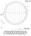
- the receptacle 1 has a plurality of pressure chambers 6, which coincide with their in the Figure 4b shown upper wall 6o form the support surface 1o.
- the pressure chambers 6 extend through the inner space 1i and face each other this sealed.
- Each of the pressure chambers 6 or groups of the pressure chambers 6 are pressurizable separately, wherein the control can be carried out by the described control device.
- the pressure chamber 6 is at least at its upper W and 6o formed so that it yields upon pressurization, so either thinner and / or softer than the other boundary walls of the pressure chamber 6 is formed.
- the openings 2 are connected to the interior 1i.
- a minimal local deflection of the mounting surface 1o by the abovementioned compensation means 3, 4, 5, 6 takes place by a maximum of 3 ⁇ m, in particular a maximum of 1 ⁇ m, preferably a maximum of 100 nm.
- the control device In order to be able to counteract the local distortions with one or more of the aforementioned embodiments, it is necessary, as described above, for the control device to know where and to what extent or in which direction distortions are present in the wafer. Only then is a targeted action or counteraction and compensation of the distortions possible.
- the expansion card of each wafer provides information in the form of distributed over the wafer strain vectors, which with a corresponding measuring device according to the EP 10 015 569.6 have been determined.
- Corresponding control data can be stored in the control unit, in particular empirically determined, in order to be able to carry out an individual control corresponding to the expansion card of the wafer at the positions predetermined by the position map of the wafer for each wafer. The compensation can be carried out in this way automatically during the alignment of the wafer.
- the active controls 3, 4, 5, 6 are not shown to scale in the figures and may also have different sizes or shapes.
Landscapes
- Container, Conveyance, Adherence, Positioning, Of Wafer (AREA)
Abstract
Description
- Die Erfindung betrifft eine Aufnahmeeinrichtung zur Aufnahme und Halterung von Wafern gemäß Patentanspruch 1 sowie eine Vorrichtung und ein Verfahren zum Ausrichten eines ersten Wafers mit einem zweiten Wafer gemäß Patentansprüchen 8 und 9 unter Verwendung der Aufnahmeeinrichtung gemäß Patentanspruch 1.
- Solche Aufnahmeeinrichtungen oder Probenhalter beziehungsweise Chucks gibt es in vielfältigen Ausführungen und entscheidend für die Aufnahmeeinrichtungen ist eine ebene Aufnahmefläche beziehungsweise Halterungsfläche, damit die immer kleiner werdenden Strukturen auf immer größeren Waferflächen über die gesamte Waferfläche korrekt ausgerichtet und kontaktiert werden können. Dies ist besonders wichtig, wenn ein sogenannter Pre-Bonding-Schritt, welcher die Wafer mittels einer trennbaren Verbindung miteinander verbindet, vor dem eigentlichen Bondvorgang durchgeführt wird. Besonders wichtig ist eine hohe Ausrichtungsgenauigkeit der Wafer zueinander, sobald für alle auf einem oder beiden Wafern angeordneten Strukturen eine Ausrichtungsgenauigkeit oder insbesondere Verzerrungswerte von < 2µm erreicht werden soll. In der Nähe von Ausrichtungsmarken gelingt dies bei bekannten Aufnahmeeinrichtungen und Vorrichtungen zur Ausrichtung, sogenannte Aligner, insbesondere Bondaligner, sehr gut. Mit zunehmendem Abstand von den Ausrichtungsmarken ist eine kontrollierte und perfekte Ausrichtung mit Ausrichtungsgenauigkeiten oder insbesondere Verzerrungswerten besser als 2µm, vorzugsweise besser als 1µm und noch bevorzugter besser als 0,25µm nicht erreichbar.
- Eine Vorrichtung zur lokalen Kompensation von Verzerrungen ist aus der
US5 094 536 A bekannt. Aus derWO 2009/133682 A1 ist ein indirektes Verfahren zur Ermittlung von Dehnungen über Positionsabweichungen von Wafermarkierungen bekannt. - Es ist die Aufgabe der vorliegenden Erfindung, gattungsgemäße Aufnahmeeinrichtungen derart zu verbessern, dass mit diesen eine genauere Ausrichtung erreicht werden kann.
- Diese Aufgabe wird mit den Merkmalen der Ansprüche 1, 8 und 9 gelöst.
- Vorteilhafte Weiterbildungen der Erfindung sind in den Unteransprüchen angegeben. In den Rahmen der Erfindung fallen auch sämtliche Kombinationen aus zumindest zwei von in der Beschreibung, den Ansprüchen und/oder den Figuren angegebenen Merkmalen. Bei angegebenen Wertebereichen sollen auch innerhalb der genannten Grenzen liegende Werte als Grenzwerte offenbart und in beliebiger Kombination beanspruchbar sein.
- Die Erfindung basiert auf der Erkenntnis der Anmelderin gemäß den europäischen Patentanmeldungen
EP 09012023 EP 10 015 569 - einer ersten Dehnungskarte von Dehnungswerten entlang einer ersten Kontaktfläche des ersten Wafers und/oder
- einer zweiten Dehnungskarte von Dehnungswerten entlang einer zweiten Kontaktfläche und
- Auswertungsmitteln zur Auswertung der ersten und/oder zweiten Dehnungskarten, durch welche die lokalen Ausrichtungsfehler ermittelbar sind.
- Grundgedanke der vorliegenden Erfindung ist es dabei, eine Aufnahmeeinrichtung bestehend aus mehreren, voneinander unabhängigen aktiven Steuerelementen vorzusehen, mit welchen die Halterungsfläche der Aufnahmeeinrichtung, insbesondere in Form und/oder Temperatur, beeinflussbar ist. Dabei werden die aktiven Steuerelemente durch entsprechende Ansteuerung so verwendet, dass die mittels der Positionskarten und/oder Dehnungskarten bekannten lokalen Ausrichtungsfehler beziehungsweise lokalen Verzerrungen kompensiert beziehungsweise weitestgehend minimiert oder reduziert werden. Dabei werden nicht nur lokale Verzerrungen beseitigt, sondern eine sich aus den lokalen Verzerrungen insgesamt ergebende makroskopische Verzerrung oder Dehnung des Wafers in seinen Außenabmessungen wird gleichzeitig minimiert beziehungsweise korrigiert.
- Somit ist es erfindungsgemäß insbesondere in Kombination mit den oben beschriebenen Erfindungen betreffend die Positionskarten, Dehnungskarten und/oder Spannungskarten sowie der dort offenbarten in-situ-Korrektur von Ausrichtungsfehlern beim Kontaktieren und Bonden der Wafer, möglich, durch aktive, insbesondere lokale Einwirkung auf Verzerrungen des Wafers ein noch besseres Ausrichtungsergebnis zu erreichen.
- Gemäß einer vorteilhaften Ausführungsform der Erfindung ist vorgesehen, dass durch die Kompensationsmittel die Temperatur der Halterungsfläche lokal beeinflussbar ist. Eine lokale Temperaturerhöhung der Halterungsfläche führt zu einer lokalen Ausdehnung des auf der Halterungsfläche gehaltenen Wafers an dieser Position. Je höher der Temperaturgradient ist, desto mehr dehnt sich der Wafer an dieser Position aus. Basierend auf den Daten der Positionskarten und / oder Dehnungskarten, insbesondere der Vektorauswertung des Ausrichtungsfehlers, insbesondere für jede Position der Positionskarten und / oder Dehnungskarten, kann so gezielt auf lokale Verzerrungen des Wafers eingewirkt beziehungsweise diesen entgegengewirkt werden.
- In diesem Zusammenhang ist als Vektorauswertung ein Vektorfeld mit Verzerrungsvektoren zu verstehen, das insbesondere mittels einer von zwei nachfolgend beschriebenen Erfindungsvarianten ermittelt wurde.
- Die erste Variante bezieht sich auf Anwendungsfälle, in denen nur einer der beiden Wafer strukturiert ist. In diesem Fall ist es erfindungsgemäß vorgesehen, die Abweichung der Strukturen, insbesondere die Abweichung der geometrischen Form von der gewünschten Form zu erfassen. Von besonderem Interesse ist in diesem Fall die Abweichung der Form von Belichtungsfeldern, insbesondere Belichtungsfeldern eines Step & Repeat Belichtungsgerätes von der nominell erwarteten Form, die üblicherweise rechteckig ist. Diese Abweichungen, insbesondere das diese Abweichungen beschreibende Vektorfeld, kann basierend auf der Erfassung einer Positionskarte der einzelnen mit den Belichtungsfeldern korrespondierenden Ausrichtungsmarken gemäß
EP 09012023 EP 10 015 569.6 - Die zweite Variante bezieht sich auf Anwendungsfälle, in denen beide Wafer strukturiert sind. In diesem Fall ist es erfindungsgemäß vorgesehen, das Vektorfeld der Ausrichtungsabweichung insbesondere für alle Positionen der Positionskarten, insbesondere der ersten und zweiten Positionskarten gemäß
EP 09012023 EP 10 015 569.6 - In einer weiteren, vorteilhaften Ausführungsform der Erfindung ist vorgesehen, dass durch die Kompensationsmittel die Dehnung der Halterungsfläche, insbesondere durch Anordnung von, vorzugsweise einzeln ansteuerbaren, Piezoelementen an einer Rückseite der Halterungsfläche, lokal beeinflussbar ist. Durch Dehnung oder Schrumpfung, also negative Dehnung, der Halterungsfläche wird, insbesondere durch die von der Halterungsfläche auf den Wafer wirkende Haltekraft, auch der Wafer entsprechend verformt, insbesondere gedehnt oder geschrumpft, so dass auf diese Weise eine gezielte Beeinflussung des Wafers durch eine entsprechende Steuerungseinrichtung basierend auf den Werten der für diesen Wafer ermittelten Dehnungskarte möglich ist. Soweit durch die Kompensationsmittel die Form der Halterungsfläche, insbesondere durch, vorzugsweise mechanische, Einwirkung in einer Z-Richtung lokal beeinflussbar ist, besteht eine weitere Möglichkeit, Verzerrungen des Wafers an der Halterungsfläche entgegenzuwirken. Auch hier gilt, dass die Steuerung der Kompensationsmittel durch eine Steuereinrichtung erfolgt, die auf Grundlage der Werte der Positions- und/oder Dehnungskarten eine entsprechend gezielte, lokale Steuerung der Kompensationsmittel vornimmt.
- Die Steuerungseinrichtung umfasst insbesondere eine Software zur Ausführung/Berechnung entsprechender Routinen.
- Gemäß einer weiteren vorteilhaften Ausführungsform der Erfindung ist vorgesehen, dass die Halterungsfläche von einer Rückseite der Halterungsfläche durch die Kompensationsmittel lokal, insbesondere hydraulisch und/oder pneumatisch, mit Druck beaufschlagbar ist. Hierdurch kann ebenfalls auf die Form der Halterungsfläche Einfluss genommen werden, so dass sich die obengenannten Effekte ergeben. Die Steuerung erfolgt ebenfalls wieder durch die oben beschriebene Steuereinrichtung.
- Mit Vorteil sind die Kompensationsmittel als eine Vielzahl aktiver Steuerelemente in der Aufnahmeeinrichtung, insbesondere in die Halterungsfläche integriert, vorzugsweise eingebettet, vorgesehen. Somit kann eine Aufnahme der Aufnahmeeinrichtung monolithisch ausgebildet sein, wie dies bei bekannten Aufnahmeeinrichtungen ebenfalls der Fall ist.
- Dabei ist es von besonderem Vorteil, wenn jedes Steuerelement oder Gruppen von Steuerelementen gesondert ansteuerbar ist/sind. Entsprechend ist mit lokaler Ansteuerung gemeint, dass ein kleiner Ausschnitt insbesondere ein Ausschnitt kleiner als die Hälfte des Wafers, vorzugsweise kleiner als 1/4 des Wafers, vorzugsweise kleiner als 1/8 des Wafers, noch bevorzugter kleiner als 1/16 des Wafers, durch die Kompensationsmittel lokal ansteuerbar ist. Besonders vorteilhaft ist es, wenn die Kompensationsmittel auf jeden von einer eigenen Struktur belegten Bereich des Wafers mit mindestens einem Steuerelement einwirken können.
- Die erfindungsgemäße Vorrichtung umfasst die vorbeschriebene Steuereinrichtung mit Vorteil in einer zentralen, für alle Steuerungsvorgänge zuständigen Steuereinheit. Erfindungsgemäß ist es jedoch denkbar, die Steuereinrichtung in der Aufnahmeeinrichtung, insbesondere als Modul einer Gesamtvorrichtung, vorzusehen.
- Das erfindungsgemäße Verfahren kann dadurch noch weiter verbessert werden, indem nach der Ausrichtung eine, insbesondere nochmalige, Erfassung von Positions- und/oder Dehnungskarten des ersten und/oder zweiten Wafers vorgesehen ist. Damit kann erfindungsgemäß nach der erfolgten Ausrichtung eine Überprüfung des Ausrichtungserfolgs vorgesehen werden. Entsprechend ist es denkbar, eine Ausgliederung eines Waferpaares mit zu großen Ausrichtungsfehlern vorzunehmen, um diese beispielsweise erneut erfindungsgemäß auszurichten oder zu entsorgen. Gleichzeitig können die erfassten Daten zur Selbstkalibrierung der Vorrichtung, insbesondere mittels der Steuereinrichtung, verwendet werden.
- Die in der europäischen Patentanmeldung
EP 09012023.9 EP 10 015 569.6 - Als mitoffenbart gelten die folgenden allgemeinen Gegenstände:
Eine Aufnahmeeinrichtung zur Aufnahme und Halterung von Wafern mit folgenden Merkmalen: - eine Halterungsfläche (1o),
- Haltemittel zur Halterung des Wafers an der Halterungsfläche (1o) und
- Kompensationsmittel (3, 4, 5, 6) zur aktiven, insbesondere lokal steuerbaren, zumindest teilweisen Kompensation von lokalen und/oder globalen Verzerrungen des Wafers.
- eine Einrichtung zur Ermittlung von durch Dehnung und/oder Verzerrung des ersten Wafers gegenüber dem zweiten Wafer beim Verbinden des ersten Wafers mit dem zweiten Wafer aufgetretenen lokalen Ausrichtungsfehlern mit einer ersten Dehnungskarte des ersten Wafers und/oder einer zweiten Dehnungskarte des zweiten Wafers und Auswertungsmitteln zur Auswertung der ersten und/oder zweiten Dehnungskarten,
- mindestens eine oben beschriebene Aufnahmeeinrichtung zur Aufnahme wenigstens eines der Wafer und
- Ausrichtungsmittel zur Ausrichtung der Wafer unter Berücksichtigung der Positionskarten und/oder Dehnungskarten sowie gleichzeitiger Kompensation durch die Kompensationsmittel.
- Erfassung einer ersten Dehnungskarte des ersten Wafers und/oder einer zweiten Dehnungskarte des zweiten Wafers und Auswertung der ersten und/oder zweiten Dehnungskarten durch Auswertungsmittel und Ermittlung der lokalen Ausrichtungsfehler,
- Aufnahme mindestens eines der Wafer auf einer oben beschriebenen Aufnahmeeinrichtung und
- Ausrichtung der Wafer unter Berücksichtigung der Positionskarten und/oder Dehnungskarten sowie gleichzeitiger Kompensation durch die Kompensationsmittel.
- Ein solches Verfahren, bei dem nach der Ausrichtung eine, insbesondere nochmalige, Erfassung von Positions- und/oder Dehnungskarten des ersten und/oder zweiten Wafers vorgesehen ist.
- Weitere Vorteile, Merkmale und Einzelheiten der Erfindung ergeben sich aus der nachfolgenden Beschreibung bevorzugter Ausführungsbeispiele sowie anhand der Zeichnungen, diese zeigen in:
- Fig. 1a
- eine Aufsicht auf eine erfindungsgemäße Aufnahmeeinrichtung in einer ersten Ausführungsform,
- Fig. 1b
- eine Querschnittsansicht der Aufnahmeeinrichtung gemäß Schnittlinie A-A aus
Figur 1a , - Fig. 2a
- eine Aufsicht auf eine erfindungsgemäße Aufnahmeeinrichtung in einer zweiten Ausführungsform,
- Fig. 2b
- eine Querschnittsansicht der Aufnahmeeinrichtung gemäß Schnittlinie B-B aus
Figur 2a , - Fig. 3a
- eine Aufsicht auf eine erfindungsgemäße Aufnahmeeinrichtung in einer dritten Ausführungsform,
- Fig. 3b
- eine Querschnittsansicht der Aufnahmeeinrichtung gemäß Schnittlinie C-C aus
Figur 3a , - Fig. 4a
- eine Aufsicht auf eine erfindungsgemäße Aufnahmeeinrichtung in einer vierten Ausführungsform und
- Fig. 4b
- eine Querschnittsansicht der Aufnahmeeinrichtung gemäß Schnittlinie D-D aus
Figur 4a . - In den Figuren sind gleiche und gleichwirkende Bauteile/Merkmale mit den gleichen Bezugszeichen gekennzeichnet.
- Alle vier Ausführungsformen zeigen eine monolithische Aufnahme 1, die als flache, vorzugsweise kreisringförmige, Platte mit einer plan ebenen Halterungsfläche 1o zur Aufnahme und Halterung von Wafern versehen ist. Am Außenumfang weist die Aufnahme einen ringförmigen Absatz 1a auf.
- Die Halterungsfläche 1o bildet eine Aufnahmeebene zur Aufnahme des Wafers, die sich in X- und Y-Richtung erstreckt. Hierzu senkrecht verläuft die Z-Richtung, in der die auf den Wafer wirkende Haltekraft gerichtet ist. Die Halterung des Wafers erfolgt durch Öffnungen 2, die in einer Vielzahl gleichförmig über die Halterungsfläche 10 verteilt angeordnet sind, um den Wafer an der Halterungsfläche 1o durch Beaufschlagung der Öffnungen 2 mit Unterdruck halten zu können. Je größer die Anzahl der Öffnungen 2 ist und je kleiner der Durchmesser der Öffnungen 2 ist, desto weniger führt der an den Öffnungen 2 anliegende Unterdruck zur Halterung des Wafers zu Verzerrungen des Wafers an den Öffnungen 2.
- Der Unterdruck an den Öffnungen 2 wird über eine nicht dargestellte Vakuumeinrichtung angelegt, die einen rückseitig der Halterungsfläche 1o angeordneten Innenraum 1i mit Unterdruck beaufschlagt. Der Innenraum 1i ist weiterhin durch eine Umfangswand 1w der Aufnahme 1 begrenzt und gegenüber der Umgebung abgedichtet. Die Öffnungen 2 erstrecken sich von der Halterungsfläche 1o bis zum Innenraum 1i und sind somit gleichmäßig mit dem im Innenraum 1i vorherrschenden Unterdruck beaufschlagbar.
- Der Innenraum 1i ist weiterhin durch eine gegenüberliegend zur Halterungsfläche 1o angeordnete Rückseite 1r und einen nicht dargestellten Boden des Innenraums 1i begrenzt, wobei die Rückseite 1r von den Öffnungen 2 durchsetzt ist.
- Als aktive Steuerelemente sind an der Rückseite 1r eine Vielzahl von Heiz-/Kühlelementen, insbesondere ausschließlich Heizelemente 3, vorgesehen. Die Heizelemente 3 sind jeweils einzeln oder in Gruppen angesteuert, wobei die Steuerung durch eine nicht dargestellte Steuereinrichtung erfolgt. Beim Aufheizen eines der Heizelemente 3 heizt sich durch das sehr gut wärmeleitende Material, insbesondere Metall, der Aufnahme ein lokaler Abschnitt der Halterungsfläche 1o auf. Dies führt zu einer lokalen Ausdehnung eines auf der Halterungsfläche 1o liegenden Wafers in diesem Bereich. Somit kann bei entsprechend ausgerichtet auf der Aufnahmeeinrichtung aufgenommenem Wafer und bekannter Position von etwaigen Verzerrungen/Dehnungen gezielt durch Schalten einzelner oder mehrerer Heizelemente 3 eine Verformung des Wafers bewirkt werden, um lokale Verzerrrungen zu kompensieren. Hierdurch ergibt sich, insbesondere bei einer Vielzahl von lokalen Kompensationen, auch eine globale Kompensation von globalen Verzerrungen, insbesondere einer Änderung des Durchmessers des Wafers in X- und/oder Y-Richtung.
- Ein besonderer Vorteil der Beeinflussung der Verzerrungen am Wafer mittels der Heiz- und / oder Kühlelemente liegt in der Möglichkeit, dies mit minimaler Verformung, insbesondere ohne Verformung der Halterungsfläche und/oder insbesondere ohne Verformung des Wafers in vertikaler Richtung beziehungsweise Z-Richtung, erreichen zu können. Als minimale Verformung in diesem Zusammenhang ist eine Verformung der Halterungsfläche und insbesondere des Wafers in vertikaler, das heißt senkrechter Richtung beziehungsweise in Z-Richtung im Verhältnis zur Auflagefläche von <5µm, mit Vorteil <2µm, bevorzugt <1µm und noch bevorzugter <0,5µm anzusehen. Dies ist insbesondere für das Herstellen von Pre-Bonding Verbindungen, beispielsweise für Pre-Bonds, die auf Van-der-Waals Verbindungen basieren, vorteilhaft. Aufgrund der Tatsache, dass hier die Halterungsfläche und insbesondere der Wafer eben gehalten werden kann, wird die bei derartigen Pre-Bonding Schritten übliche Bondwelle nicht in ihrer Ausbreitung durch Unebenheiten beeinflusst. Damit wird das Risiko, dass ungebondete Stellen (sogenannte Voids) verbleiben, stark reduziert. Für das Herstellen derartiger Pre-Bonding Verbindungen wird erfindungsgemäß eine Ebenheit der Halterungsfläche von <5µm, mit Vorteil <2µm, bevorzugt <1µm und noch bevorzugter <0,5µm über die gesamte Waferfläche angestrebt. Mit diesen Ebenheitswerten ist der Abstand zwischen dem höchsten und dem niedrigsten Punkt innerhalb jenes Teiles der Haltefläche, der mit dem Wafer in Kontakt ist, gemeint.
- Die Heizelemente 3 sind mit Vorteil gleichmäßig unter der Halterungsfläche 1o verteilt. Mit Vorteil sind mehr als 10 Heizelemente 3, insbesondere mehr als 50 Heizelemente 3, vorzugsweise mehr als 100 Heizelemente 3, noch bevorzugter mehr als 500 Heizelemente 3, in der Aufnahmeeinrichtung vorgesehen. Diese Heizelemente bilden separat ansteuerbare Bereiche in der Halterungsfläche, die lokales Einwirken auf den Wafer ermöglichen. Mit Vorteil sind die einzelnen Bereiche der Halterungsfläche mit geeigneten Mitteln thermisch voneinander isoliert. Insbesondere sind die Bereiche in einer Form ausgebildet, die eine gleichmäßige und geschlossene Anordnung der einzelnen Segmente ermöglicht. Mit Vorteil eignet sich dafür die Ausbildung der Segmente als Dreiecke, Vierecke oder Sechsecke.
- Als Heizelemente 3 sind insbesondere Peltierelemente geeignet.
- In der in den
Figuren 2a und 2b gezeigten zweiten Ausführungsform sind keine Heizelemente 3 gezeigt und stattdessen oder in Kombination mit diesen sind Piezoelemente 4 an der Halterungsfläche 1o vorgesehen, vorzugsweise mit einem größeren Abstand zu der Rückseite 1r als zur Halterungsfläche 1o. Auf diese Weise ist ein gezieltes Einwirken auf die Halterungsfläche 1o möglich. Die Piezoelemente 4 können bei Aktivierung Dehnungen im Nanobis Mikrometerbereich bewirken. - Die Zahl der Piezoelemente 4 kann der obengenannten Zahl der Heizelemente 3 entsprechen, wobei eine Kombination der beiden Ausführungsformen erfindungsgemäß denkbar ist.
- In der in den
Figuren 3a und 3b gezeigten dritten Ausführungsform der Erfindung sind statt oder in Kombination mit den Heizelementen 3 und/oder den Piezoelementen 4 Stifte 5 vorgesehen, die an der Halterungsfläche 1o mit einem, insbesondere spitzen, Stiftende 5e enden. In der Ausgangslage der Stifte 5 ist das Stiftende 5e bündig mit der Halterungsfläche 1o. Soweit eine lokale Verzerrung eines Wafers im Bereich eines bestimmten Stiftes 5 als Information der Verzerrungskarte oder Dehnungskarte vorliegt, kann die Steuereinrichtung durch Ansteuerung einzelner oder mehrerer Stifte 5 lokal auf den Wafer einwirken, indem der Stift 5 beziehungsweise das Stiftende 5e in Z-Richtung in Richtung des Wafers bewegt wird. Das Stiftende 5e beaufschlägt damit den Wafer lokal mit einer Druckkraft, die für eine lokale Ausbeulung beziehungsweise Auslenkung des Wafers an dieser Stelle Sorge trägt. Der Stift 5 kann entweder als Ganzes in einer Führungsöffnung 7, die sich von der Halterungsfläche 1o bis zur Rückseite 1r erstreckt, gleitend geführt sein. Alternativ dazu ist nur das Stiftende 5e in dem Stift 5 bewegbar und der Stift 5 beziehungsweise der untere Abschnitt des Stifts gegenüber der Führungsöffnung 7 fixiert. Auf diese Weise kann eine besondere Abdichtung des Stifts 5 beziehungsweise der Stifte 5 gegenüber dem Innenraum 1r gewährleistet werden. - Die Anzahl der Stifte 5 entspricht der Anzahl der Piezoelemente 4 oder Heizelemente 3, wobei auch hier eine Kombination mit einer oder mehrerer der vorgenannten Ausführungsformen möglich ist.
- In der in
Figur 4 gezeigten Ausführungsform weist die Aufnahme 1 eine Vielzahl von Druckkammern 6 auf, die mit ihrer in derAbbildung 4b gezeigten oberen Wand 6o die Halterungsfläche 1o bilden. Die Druckkammern 6 erstrecken sich durch den Innenraum 1i und sind gegenüber diesem abgedichtet. Jede der Druckkammern 6 oder Gruppen der Druckkammern 6 sind gesondert druckbeaufschlagbar, wobei die Steuerung durch die beschriebene Steuereinrichtung erfolgen kann. Bei Druckbeaufschlagung ist die Druckkammer 6 zumindest an ihrer oberen W and 6o so ausgebildet, dass diese bei Druckbeaufschlagung nachgibt, also entweder dünner und/oder weicher als die anderen Begrenzungswände der Druckkammer 6 ausgebildet ist. Die Öffnungen 2 sind mit dem Innenraum 1i verbunden. - Erfindungsgemäß erfolgt eine lediglich minimale lokale Auslenkung der Halterungsfläche 1o durch die vorgenannten Kompensationsmittel 3, 4, 5, 6 um maximal 3µm, insbesondere maximal 1µm, vorzugsweise maximal 100 nm.
- Um den lokalen Verzerrungen mit einer oder mehrerer der vorgenannten Ausführungsformen entgegenwirken zu können, ist es wie oben beschrieben notwendig, dass die Steuereinrichtung weiß, wo und in welchem Umfang beziehungsweise in welcher Richtung Verzerrungen im Wafer vorliegen. Erst dann ist ein gezieltes Einwirken beziehungsweise Entgegenwirken und Kompensieren der Verzerrungen möglich. Die Dehnungskarte eines jeden Wafers ergibt Aufschluss in Form von über den Wafer verteilten Dehnungsvektoren, die mit einer entsprechenden Messeinrichtung gemäß der
EP 10 015 569.6 - Die aktiven Steuerelemente 3, 4, 5, 6 sind in den Figuren nicht maßstabsgetreu abgebildet und können auch verschiedene Größen oder Formen aufweisen.
-
- 1
- Aufnahme
- 1a
- ringförmiger Absatz
- 1i
- Innenraum
- 1o
- Halterungsfläche
- 1w
- Umfangswand
- 2
- Öffnungen
- 3
- Heiz-/Kühlelemente
- 4
- Piezoelemente
- 5
- Stifte
- 5e
- Stiftende
- 6
- Druckkammern
- 6o
- obere Wand
- 7
- Führungsöffnung
Eine solche Aufnahmeeinrichtung nach einem der vorhergehenden Ansprüche, bei der durch die Kompensationsmittel die Dehnung der Halterungsfläche (lo), insbesondere durch Anordnung von vorzugsweise einzeln ansteuerbaren, Piezoelementen an einer Rückseite der Halterungsfläche, lokal beeinflussbar ist.
Eine solche Aufnahmeeinrichtung, bei der die Kompensationsmittel als eine Vielzahl aktiver Steuerelemente in der Aufnahmeeinrichtung, insbesondere in die Halterungsfläche integriert, vorzugsweise eingebettet, vorgesehen sind. Eine solche Aufnahmeeinrichtung, bei der jedes Steuerelement oder Gruppen von Steuerelementen gesondert ansteuerbar ist/sind.
Eine Vorrichtung zum Ausrichten eines ersten Wafers mit einem zweiten Wafer mit folgenden Merkmalen:
Claims (9)
- Aufnahmeeinrichtung zur Aufnahme und Halterung von Wafern mit folgenden Merkmalen:- eine Halterungsfläche (1o),- Haltemittel zur Halterung des Wafers an der Halterungsfläche (1o) und- Kompensationsmittel (3, 4, 5, 6) zur aktiven, zumindest teilweisen Kompensation von globalen Verzerrungen des Wafers, wobei die Halterungsfläche (1o) von einer Rückseite (1r) der Halterungsfläche (1o) durch die Kompensationsmittel (3, 4, 5, 6) lokal, nämlich hydraulisch und/oder pneumatisch, mit Druck beaufschlagbar ist.
- Aufnahmeeinrichtung nach Anspruch 1, bei der durch die Kompensationsmittel (3, 4, 5, 6) die Temperatur der Halterungsfläche (1o) lokal beeinflussbar ist.
- Aufnahmeeinrichtung nach einem der vorhergehenden Ansprüche, bei der durch die Kompensationsmittel (3, 4, 5, 6) die Dehnung der Halterungsfläche (lo), insbesondere durch Anordnung von vorzugsweise einzeln ansteuerbaren, Piezoelementen (4) an einer Rückseite (1r) der Halterungsfläche (lo), lokal beeinflussbar ist.
- Aufnahmeeinrichtung nach einem der vorhergehenden Ansprüche, dadurch gekennzeichnet, dass durch die Kompensationsmittel (3, 4, 5, 6) die Form der Halterungsfläche (lo), insbesondere durch, vorzugsweise mechanische, Einwirkung in einer Z-Richtung, lokal beeinflussbar ist.
- Aufnahmeeinrichtung nach einem der vorhergehenden Ansprüche, bei der die Kompensationsmittel (3, 4, 5, 6) als eine Vielzahl aktiver Steuerelemente (3, 4, 5, 6) in der Aufnahmeeinrichtung, insbesondere in die Halterungsfläche (1o) integriert, vorzugsweise eingebettet, vorgesehen sind.
- Aufnahmeeinrichtung nach Anspruch 6, bei der jedes Steuerelement (3, 4, 5, 6) oder Gruppen von Steuerelementen (3, 4, 5, 6) gesondert ansteuerbar ist/sind.
- Vorrichtung zum Ausrichten eines ersten Wafers mit einem zweiten Wafer mit folgenden Merkmalen:- eine Einrichtung zur Ermittlung von durch Dehnung und/oder Verzerrung des ersten Wafers gegenüber dem zweiten Wafer beim Verbinden des ersten Wafers mit dem zweiten Wafer aufgetretenen lokalen Ausrichtungsfehlern in Form eines Vektorfelds mit Verzerrungsvektoren,- mindestens eine Aufnahmeeinrichtung nach einem der vorhergehenden Ansprüche zur Aufnahme wenigstens eines der Wafer und- Ausrichtungsmittel zur Ausrichtung der Wafer unter Berücksichtigung des Vektorfelds sowie gleichzeitiger Kompensation durch die Kompensationsmittel.
- Verfahren zum Ausrichten eines ersten Wafers mit einem zweiten Wafer mit folgenden Schritten, insbesondere folgendem Ablauf:- Erfassung eines Vektorfelds mit Verzerrungsvektoren des ersten Wafers und/oder eines Vektorfelds mit Verzerrungsvektoren des zweiten Wafers und Auswertung des Vektorfelds durch Auswertungsmittel und Ermittlung der lokalen Ausrichtungsfehler,- Aufnahme mindestens eines der Wafer auf einer Aufnahmeeinrichtung nach einem der Ansprüche 1 bis 6 und- Ausrichtung der Wafer unter Berücksichtigung des Vektorfelds sowie gleichzeitiger Kompensation durch die Kompensationsmittel.
- Verfahren nach Anspruch 8, bei dem nach der Ausrichtung eine, insbesondere nochmalige, Erfassung eines Vektorfelds des ersten und/oder zweiten Wafers vorgesehen ist.
Priority Applications (2)
| Application Number | Priority Date | Filing Date | Title |
|---|---|---|---|
| EP23205746.3A EP4290563A3 (de) | 2010-12-20 | 2010-12-20 | Aufnahmeeinrichtung zur halterung von wafern |
| EP18202622.9A EP3460833B1 (de) | 2010-12-20 | 2010-12-20 | Aufnahmeeinrichtung zur halterung von wafern |
Applications Claiming Priority (4)
| Application Number | Priority Date | Filing Date | Title |
|---|---|---|---|
| EP10803232.7A EP2656378B1 (de) | 2010-12-20 | 2010-12-20 | Aufnahmeeinrichtung zur halterung von wafern |
| PCT/EP2010/007793 WO2012083978A1 (de) | 2010-12-20 | 2010-12-20 | Aufnahmeeinrichtung zur halterung von wafern |
| EP14199922.7A EP2854157B1 (de) | 2010-12-20 | 2010-12-20 | Aufnahmeeinrichtung zur Halterung von Wafern |
| EP18202622.9A EP3460833B1 (de) | 2010-12-20 | 2010-12-20 | Aufnahmeeinrichtung zur halterung von wafern |
Related Parent Applications (3)
| Application Number | Title | Priority Date | Filing Date |
|---|---|---|---|
| EP10803232.7A Division EP2656378B1 (de) | 2010-12-20 | 2010-12-20 | Aufnahmeeinrichtung zur halterung von wafern |
| EP14199922.7A Division EP2854157B1 (de) | 2010-12-20 | 2010-12-20 | Aufnahmeeinrichtung zur Halterung von Wafern |
| EP14199922.7A Division-Into EP2854157B1 (de) | 2010-12-20 | 2010-12-20 | Aufnahmeeinrichtung zur Halterung von Wafern |
Related Child Applications (2)
| Application Number | Title | Priority Date | Filing Date |
|---|---|---|---|
| EP23205746.3A Division EP4290563A3 (de) | 2010-12-20 | 2010-12-20 | Aufnahmeeinrichtung zur halterung von wafern |
| EP23205746.3A Division-Into EP4290563A3 (de) | 2010-12-20 | 2010-12-20 | Aufnahmeeinrichtung zur halterung von wafern |
Publications (2)
| Publication Number | Publication Date |
|---|---|
| EP3460833A1 true EP3460833A1 (de) | 2019-03-27 |
| EP3460833B1 EP3460833B1 (de) | 2023-12-06 |
Family
ID=43982251
Family Applications (5)
| Application Number | Title | Priority Date | Filing Date |
|---|---|---|---|
| EP18202622.9A Active EP3460833B1 (de) | 2010-12-20 | 2010-12-20 | Aufnahmeeinrichtung zur halterung von wafern |
| EP23205746.3A Pending EP4290563A3 (de) | 2010-12-20 | 2010-12-20 | Aufnahmeeinrichtung zur halterung von wafern |
| EP10803232.7A Active EP2656378B1 (de) | 2010-12-20 | 2010-12-20 | Aufnahmeeinrichtung zur halterung von wafern |
| EP15150980.9A Active EP2863421B1 (de) | 2010-12-20 | 2010-12-20 | Aufnahmeeinrichtung zur Halterung von Wafern |
| EP14199922.7A Active EP2854157B1 (de) | 2010-12-20 | 2010-12-20 | Aufnahmeeinrichtung zur Halterung von Wafern |
Family Applications After (4)
| Application Number | Title | Priority Date | Filing Date |
|---|---|---|---|
| EP23205746.3A Pending EP4290563A3 (de) | 2010-12-20 | 2010-12-20 | Aufnahmeeinrichtung zur halterung von wafern |
| EP10803232.7A Active EP2656378B1 (de) | 2010-12-20 | 2010-12-20 | Aufnahmeeinrichtung zur halterung von wafern |
| EP15150980.9A Active EP2863421B1 (de) | 2010-12-20 | 2010-12-20 | Aufnahmeeinrichtung zur Halterung von Wafern |
| EP14199922.7A Active EP2854157B1 (de) | 2010-12-20 | 2010-12-20 | Aufnahmeeinrichtung zur Halterung von Wafern |
Country Status (8)
| Country | Link |
|---|---|
| US (5) | US9312161B2 (de) |
| EP (5) | EP3460833B1 (de) |
| JP (1) | JP6279324B2 (de) |
| KR (5) | KR101866719B1 (de) |
| CN (2) | CN106887399B (de) |
| SG (1) | SG187694A1 (de) |
| TW (4) | TWI563548B (de) |
| WO (1) | WO2012083978A1 (de) |
Cited By (2)
| Publication number | Priority date | Publication date | Assignee | Title |
|---|---|---|---|---|
| US11782411B2 (en) | 2021-07-28 | 2023-10-10 | Kla Corporation | System and method for mitigating overlay distortion patterns caused by a wafer bonding tool |
| US11829077B2 (en) | 2020-12-11 | 2023-11-28 | Kla Corporation | System and method for determining post bonding overlay |
Families Citing this family (439)
| Publication number | Priority date | Publication date | Assignee | Title |
|---|---|---|---|---|
| US10378106B2 (en) | 2008-11-14 | 2019-08-13 | Asm Ip Holding B.V. | Method of forming insulation film by modified PEALD |
| US9394608B2 (en) | 2009-04-06 | 2016-07-19 | Asm America, Inc. | Semiconductor processing reactor and components thereof |
| US8802201B2 (en) | 2009-08-14 | 2014-08-12 | Asm America, Inc. | Systems and methods for thin-film deposition of metal oxides using excited nitrogen-oxygen species |
| KR101866719B1 (ko) * | 2010-12-20 | 2018-06-11 | 에베 그룹 에. 탈너 게엠베하 | 웨이퍼의 장착을 위한 수용 수단 |
| US9312155B2 (en) | 2011-06-06 | 2016-04-12 | Asm Japan K.K. | High-throughput semiconductor-processing apparatus equipped with multiple dual-chamber modules |
| US9793148B2 (en) | 2011-06-22 | 2017-10-17 | Asm Japan K.K. | Method for positioning wafers in multiple wafer transport |
| US10364496B2 (en) | 2011-06-27 | 2019-07-30 | Asm Ip Holding B.V. | Dual section module having shared and unshared mass flow controllers |
| US10854498B2 (en) | 2011-07-15 | 2020-12-01 | Asm Ip Holding B.V. | Wafer-supporting device and method for producing same |
| US20130023129A1 (en) | 2011-07-20 | 2013-01-24 | Asm America, Inc. | Pressure transmitter for a semiconductor processing environment |
| US9017481B1 (en) | 2011-10-28 | 2015-04-28 | Asm America, Inc. | Process feed management for semiconductor substrate processing |
| US8946830B2 (en) | 2012-04-04 | 2015-02-03 | Asm Ip Holdings B.V. | Metal oxide protective layer for a semiconductor device |
| US9558931B2 (en) | 2012-07-27 | 2017-01-31 | Asm Ip Holding B.V. | System and method for gas-phase sulfur passivation of a semiconductor surface |
| US9659799B2 (en) | 2012-08-28 | 2017-05-23 | Asm Ip Holding B.V. | Systems and methods for dynamic semiconductor process scheduling |
| USD723239S1 (en) * | 2012-08-30 | 2015-02-24 | Entegris, Inc. | Wafer carrier ring |
| US9021985B2 (en) | 2012-09-12 | 2015-05-05 | Asm Ip Holdings B.V. | Process gas management for an inductively-coupled plasma deposition reactor |
| US9324811B2 (en) | 2012-09-26 | 2016-04-26 | Asm Ip Holding B.V. | Structures and devices including a tensile-stressed silicon arsenic layer and methods of forming same |
| US10714315B2 (en) | 2012-10-12 | 2020-07-14 | Asm Ip Holdings B.V. | Semiconductor reaction chamber showerhead |
| US9640416B2 (en) | 2012-12-26 | 2017-05-02 | Asm Ip Holding B.V. | Single-and dual-chamber module-attachable wafer-handling chamber |
| US20160376700A1 (en) | 2013-02-01 | 2016-12-29 | Asm Ip Holding B.V. | System for treatment of deposition reactor |
| US9589770B2 (en) | 2013-03-08 | 2017-03-07 | Asm Ip Holding B.V. | Method and systems for in-situ formation of intermediate reactive species |
| US9484191B2 (en) | 2013-03-08 | 2016-11-01 | Asm Ip Holding B.V. | Pulsed remote plasma method and system |
| KR102776049B1 (ko) | 2013-05-29 | 2025-03-04 | 에베 그룹 에. 탈너 게엠베하 | 기판을 결합하기 위한 방법 및 장치 |
| US9058974B2 (en) * | 2013-06-03 | 2015-06-16 | International Business Machines Corporation | Distorting donor wafer to corresponding distortion of host wafer |
| US8993054B2 (en) | 2013-07-12 | 2015-03-31 | Asm Ip Holding B.V. | Method and system to reduce outgassing in a reaction chamber |
| US9018111B2 (en) | 2013-07-22 | 2015-04-28 | Asm Ip Holding B.V. | Semiconductor reaction chamber with plasma capabilities |
| US9793115B2 (en) | 2013-08-14 | 2017-10-17 | Asm Ip Holding B.V. | Structures and devices including germanium-tin films and methods of forming same |
| US9059039B2 (en) * | 2013-09-06 | 2015-06-16 | International Business Machines Corporation | Reducing wafer bonding misalignment by varying thermal treatment prior to bonding |
| JP6178683B2 (ja) * | 2013-09-25 | 2017-08-09 | 芝浦メカトロニクス株式会社 | 吸着ステージ、貼合装置、および貼合方法 |
| US9240412B2 (en) | 2013-09-27 | 2016-01-19 | Asm Ip Holding B.V. | Semiconductor structure and device and methods of forming same using selective epitaxial process |
| US9556516B2 (en) | 2013-10-09 | 2017-01-31 | ASM IP Holding B.V | Method for forming Ti-containing film by PEALD using TDMAT or TDEAT |
| US10179947B2 (en) | 2013-11-26 | 2019-01-15 | Asm Ip Holding B.V. | Method for forming conformal nitrided, oxidized, or carbonized dielectric film by atomic layer deposition |
| US10683571B2 (en) | 2014-02-25 | 2020-06-16 | Asm Ip Holding B.V. | Gas supply manifold and method of supplying gases to chamber using same |
| US10167557B2 (en) | 2014-03-18 | 2019-01-01 | Asm Ip Holding B.V. | Gas distribution system, reactor including the system, and methods of using the same |
| US9447498B2 (en) | 2014-03-18 | 2016-09-20 | Asm Ip Holding B.V. | Method for performing uniform processing in gas system-sharing multiple reaction chambers |
| US11015245B2 (en) | 2014-03-19 | 2021-05-25 | Asm Ip Holding B.V. | Gas-phase reactor and system having exhaust plenum and components thereof |
| US9343350B2 (en) * | 2014-04-03 | 2016-05-17 | Asm Ip Holding B.V. | Anti-slip end effector for transporting workpiece using van der waals force |
| US9404587B2 (en) | 2014-04-24 | 2016-08-02 | ASM IP Holding B.V | Lockout tagout for semiconductor vacuum valve |
| DE102014106100A1 (de) * | 2014-04-30 | 2015-11-05 | Ev Group E. Thallner Gmbh | Verfahren und Vorrichtung zum Vergleichmäßigen eines Substratstapels |
| US10858737B2 (en) | 2014-07-28 | 2020-12-08 | Asm Ip Holding B.V. | Showerhead assembly and components thereof |
| US9543180B2 (en) | 2014-08-01 | 2017-01-10 | Asm Ip Holding B.V. | Apparatus and method for transporting wafers between wafer carrier and process tool under vacuum |
| US9890456B2 (en) | 2014-08-21 | 2018-02-13 | Asm Ip Holding B.V. | Method and system for in situ formation of gas-phase compounds |
| US9657845B2 (en) | 2014-10-07 | 2017-05-23 | Asm Ip Holding B.V. | Variable conductance gas distribution apparatus and method |
| US10941490B2 (en) | 2014-10-07 | 2021-03-09 | Asm Ip Holding B.V. | Multiple temperature range susceptor, assembly, reactor and system including the susceptor, and methods of using the same |
| KR102300403B1 (ko) | 2014-11-19 | 2021-09-09 | 에이에스엠 아이피 홀딩 비.브이. | 박막 증착 방법 |
| KR102263121B1 (ko) | 2014-12-22 | 2021-06-09 | 에이에스엠 아이피 홀딩 비.브이. | 반도체 소자 및 그 제조 방법 |
| US9478415B2 (en) | 2015-02-13 | 2016-10-25 | Asm Ip Holding B.V. | Method for forming film having low resistance and shallow junction depth |
| USD767234S1 (en) * | 2015-03-02 | 2016-09-20 | Entegris, Inc. | Wafer support ring |
| US10529542B2 (en) | 2015-03-11 | 2020-01-07 | Asm Ip Holdings B.V. | Cross-flow reactor and method |
| US10276355B2 (en) | 2015-03-12 | 2019-04-30 | Asm Ip Holding B.V. | Multi-zone reactor, system including the reactor, and method of using the same |
| US10458018B2 (en) | 2015-06-26 | 2019-10-29 | Asm Ip Holding B.V. | Structures including metal carbide material, devices including the structures, and methods of forming same |
| US10600673B2 (en) | 2015-07-07 | 2020-03-24 | Asm Ip Holding B.V. | Magnetic susceptor to baseplate seal |
| US10043661B2 (en) | 2015-07-13 | 2018-08-07 | Asm Ip Holding B.V. | Method for protecting layer by forming hydrocarbon-based extremely thin film |
| US9899291B2 (en) | 2015-07-13 | 2018-02-20 | Asm Ip Holding B.V. | Method for protecting layer by forming hydrocarbon-based extremely thin film |
| US10083836B2 (en) | 2015-07-24 | 2018-09-25 | Asm Ip Holding B.V. | Formation of boron-doped titanium metal films with high work function |
| US10087525B2 (en) | 2015-08-04 | 2018-10-02 | Asm Ip Holding B.V. | Variable gap hard stop design |
| US9647114B2 (en) | 2015-08-14 | 2017-05-09 | Asm Ip Holding B.V. | Methods of forming highly p-type doped germanium tin films and structures and devices including the films |
| US9711345B2 (en) | 2015-08-25 | 2017-07-18 | Asm Ip Holding B.V. | Method for forming aluminum nitride-based film by PEALD |
| US9960072B2 (en) | 2015-09-29 | 2018-05-01 | Asm Ip Holding B.V. | Variable adjustment for precise matching of multiple chamber cavity housings |
| US9909214B2 (en) | 2015-10-15 | 2018-03-06 | Asm Ip Holding B.V. | Method for depositing dielectric film in trenches by PEALD |
| US10211308B2 (en) | 2015-10-21 | 2019-02-19 | Asm Ip Holding B.V. | NbMC layers |
| US10322384B2 (en) | 2015-11-09 | 2019-06-18 | Asm Ip Holding B.V. | Counter flow mixer for process chamber |
| US9455138B1 (en) | 2015-11-10 | 2016-09-27 | Asm Ip Holding B.V. | Method for forming dielectric film in trenches by PEALD using H-containing gas |
| US9905420B2 (en) | 2015-12-01 | 2018-02-27 | Asm Ip Holding B.V. | Methods of forming silicon germanium tin films and structures and devices including the films |
| US9607837B1 (en) | 2015-12-21 | 2017-03-28 | Asm Ip Holding B.V. | Method for forming silicon oxide cap layer for solid state diffusion process |
| US9735024B2 (en) | 2015-12-28 | 2017-08-15 | Asm Ip Holding B.V. | Method of atomic layer etching using functional group-containing fluorocarbon |
| US9627221B1 (en) | 2015-12-28 | 2017-04-18 | Asm Ip Holding B.V. | Continuous process incorporating atomic layer etching |
| US11139308B2 (en) | 2015-12-29 | 2021-10-05 | Asm Ip Holding B.V. | Atomic layer deposition of III-V compounds to form V-NAND devices |
| EP3417477B1 (de) | 2016-02-16 | 2020-01-29 | EV Group E. Thallner GmbH | Verfahren zum bonden von substraten |
| KR20220025929A (ko) | 2016-02-16 | 2022-03-03 | 에베 그룹 에. 탈너 게엠베하 | 기판 결합 방법 |
| DE202016000967U1 (de) | 2016-02-16 | 2016-03-31 | Ev Group E. Thallner Gmbh | Aufnahmeeinrichtung zur Halterung von Wafern |
| US10468251B2 (en) | 2016-02-19 | 2019-11-05 | Asm Ip Holding B.V. | Method for forming spacers using silicon nitride film for spacer-defined multiple patterning |
| US10529554B2 (en) | 2016-02-19 | 2020-01-07 | Asm Ip Holding B.V. | Method for forming silicon nitride film selectively on sidewalls or flat surfaces of trenches |
| US9754779B1 (en) | 2016-02-19 | 2017-09-05 | Asm Ip Holding B.V. | Method for forming silicon nitride film selectively on sidewalls or flat surfaces of trenches |
| US10501866B2 (en) | 2016-03-09 | 2019-12-10 | Asm Ip Holding B.V. | Gas distribution apparatus for improved film uniformity in an epitaxial system |
| US10343920B2 (en) | 2016-03-18 | 2019-07-09 | Asm Ip Holding B.V. | Aligned carbon nanotubes |
| EP3433875B1 (de) | 2016-03-22 | 2022-05-04 | EV Group E. Thallner GmbH | Verfahren zum bonden von substraten |
| US9892913B2 (en) | 2016-03-24 | 2018-02-13 | Asm Ip Holding B.V. | Radial and thickness control via biased multi-port injection settings |
| US10865475B2 (en) | 2016-04-21 | 2020-12-15 | Asm Ip Holding B.V. | Deposition of metal borides and silicides |
| US10190213B2 (en) | 2016-04-21 | 2019-01-29 | Asm Ip Holding B.V. | Deposition of metal borides |
| US10087522B2 (en) | 2016-04-21 | 2018-10-02 | Asm Ip Holding B.V. | Deposition of metal borides |
| US10367080B2 (en) | 2016-05-02 | 2019-07-30 | Asm Ip Holding B.V. | Method of forming a germanium oxynitride film |
| US10032628B2 (en) | 2016-05-02 | 2018-07-24 | Asm Ip Holding B.V. | Source/drain performance through conformal solid state doping |
| KR102592471B1 (ko) | 2016-05-17 | 2023-10-20 | 에이에스엠 아이피 홀딩 비.브이. | 금속 배선 형성 방법 및 이를 이용한 반도체 장치의 제조 방법 |
| US11453943B2 (en) | 2016-05-25 | 2022-09-27 | Asm Ip Holding B.V. | Method for forming carbon-containing silicon/metal oxide or nitride film by ALD using silicon precursor and hydrocarbon precursor |
| US10388509B2 (en) | 2016-06-28 | 2019-08-20 | Asm Ip Holding B.V. | Formation of epitaxial layers via dislocation filtering |
| US9859151B1 (en) | 2016-07-08 | 2018-01-02 | Asm Ip Holding B.V. | Selective film deposition method to form air gaps |
| US10612137B2 (en) | 2016-07-08 | 2020-04-07 | Asm Ip Holdings B.V. | Organic reactants for atomic layer deposition |
| US9793135B1 (en) | 2016-07-14 | 2017-10-17 | ASM IP Holding B.V | Method of cyclic dry etching using etchant film |
| US10714385B2 (en) | 2016-07-19 | 2020-07-14 | Asm Ip Holding B.V. | Selective deposition of tungsten |
| KR102354490B1 (ko) | 2016-07-27 | 2022-01-21 | 에이에스엠 아이피 홀딩 비.브이. | 기판 처리 방법 |
| US10177025B2 (en) | 2016-07-28 | 2019-01-08 | Asm Ip Holding B.V. | Method and apparatus for filling a gap |
| US9812320B1 (en) | 2016-07-28 | 2017-11-07 | Asm Ip Holding B.V. | Method and apparatus for filling a gap |
| KR102532607B1 (ko) | 2016-07-28 | 2023-05-15 | 에이에스엠 아이피 홀딩 비.브이. | 기판 가공 장치 및 그 동작 방법 |
| US9887082B1 (en) | 2016-07-28 | 2018-02-06 | Asm Ip Holding B.V. | Method and apparatus for filling a gap |
| US10395919B2 (en) | 2016-07-28 | 2019-08-27 | Asm Ip Holding B.V. | Method and apparatus for filling a gap |
| KR102300481B1 (ko) | 2016-08-12 | 2021-09-10 | 에베 그룹 에. 탈너 게엠베하 | 기판을 접합하기 위한 방법 및 샘플 홀더 |
| EP3504733B1 (de) | 2016-08-29 | 2020-09-23 | EV Group E. Thallner GmbH | Verfahren und vorrichtung zum ausrichten von substraten |
| US10090316B2 (en) | 2016-09-01 | 2018-10-02 | Asm Ip Holding B.V. | 3D stacked multilayer semiconductor memory using doped select transistor channel |
| US10410943B2 (en) | 2016-10-13 | 2019-09-10 | Asm Ip Holding B.V. | Method for passivating a surface of a semiconductor and related systems |
| US10643826B2 (en) | 2016-10-26 | 2020-05-05 | Asm Ip Holdings B.V. | Methods for thermally calibrating reaction chambers |
| US11532757B2 (en) | 2016-10-27 | 2022-12-20 | Asm Ip Holding B.V. | Deposition of charge trapping layers |
| US10435790B2 (en) | 2016-11-01 | 2019-10-08 | Asm Ip Holding B.V. | Method of subatmospheric plasma-enhanced ALD using capacitively coupled electrodes with narrow gap |
| US10643904B2 (en) | 2016-11-01 | 2020-05-05 | Asm Ip Holdings B.V. | Methods for forming a semiconductor device and related semiconductor device structures |
| US10714350B2 (en) | 2016-11-01 | 2020-07-14 | ASM IP Holdings, B.V. | Methods for forming a transition metal niobium nitride film on a substrate by atomic layer deposition and related semiconductor device structures |
| US10229833B2 (en) | 2016-11-01 | 2019-03-12 | Asm Ip Holding B.V. | Methods for forming a transition metal nitride film on a substrate by atomic layer deposition and related semiconductor device structures |
| US10134757B2 (en) | 2016-11-07 | 2018-11-20 | Asm Ip Holding B.V. | Method of processing a substrate and a device manufactured by using the method |
| KR102546317B1 (ko) | 2016-11-15 | 2023-06-21 | 에이에스엠 아이피 홀딩 비.브이. | 기체 공급 유닛 및 이를 포함하는 기판 처리 장치 |
| US10340135B2 (en) | 2016-11-28 | 2019-07-02 | Asm Ip Holding B.V. | Method of topologically restricted plasma-enhanced cyclic deposition of silicon or metal nitride |
| KR102762543B1 (ko) | 2016-12-14 | 2025-02-05 | 에이에스엠 아이피 홀딩 비.브이. | 기판 처리 장치 |
| US9916980B1 (en) | 2016-12-15 | 2018-03-13 | Asm Ip Holding B.V. | Method of forming a structure on a substrate |
| US11581186B2 (en) | 2016-12-15 | 2023-02-14 | Asm Ip Holding B.V. | Sequential infiltration synthesis apparatus |
| US11447861B2 (en) | 2016-12-15 | 2022-09-20 | Asm Ip Holding B.V. | Sequential infiltration synthesis apparatus and a method of forming a patterned structure |
| KR102700194B1 (ko) | 2016-12-19 | 2024-08-28 | 에이에스엠 아이피 홀딩 비.브이. | 기판 처리 장치 |
| US10269558B2 (en) | 2016-12-22 | 2019-04-23 | Asm Ip Holding B.V. | Method of forming a structure on a substrate |
| US10867788B2 (en) | 2016-12-28 | 2020-12-15 | Asm Ip Holding B.V. | Method of forming a structure on a substrate |
| US11390950B2 (en) | 2017-01-10 | 2022-07-19 | Asm Ip Holding B.V. | Reactor system and method to reduce residue buildup during a film deposition process |
| US10655221B2 (en) | 2017-02-09 | 2020-05-19 | Asm Ip Holding B.V. | Method for depositing oxide film by thermal ALD and PEALD |
| US10468261B2 (en) | 2017-02-15 | 2019-11-05 | Asm Ip Holding B.V. | Methods for forming a metallic film on a substrate by cyclical deposition and related semiconductor device structures |
| WO2018166605A1 (de) | 2017-03-16 | 2018-09-20 | Ev Group E. Thallner Gmbh | Verfahren zum bonden von mindestens drei substraten |
| US10283353B2 (en) | 2017-03-29 | 2019-05-07 | Asm Ip Holding B.V. | Method of reforming insulating film deposited on substrate with recess pattern |
| US10529563B2 (en) | 2017-03-29 | 2020-01-07 | Asm Ip Holdings B.V. | Method for forming doped metal oxide films on a substrate by cyclical deposition and related semiconductor device structures |
| US10103040B1 (en) | 2017-03-31 | 2018-10-16 | Asm Ip Holding B.V. | Apparatus and method for manufacturing a semiconductor device |
| USD830981S1 (en) | 2017-04-07 | 2018-10-16 | Asm Ip Holding B.V. | Susceptor for semiconductor substrate processing apparatus |
| KR102457289B1 (ko) | 2017-04-25 | 2022-10-21 | 에이에스엠 아이피 홀딩 비.브이. | 박막 증착 방법 및 반도체 장치의 제조 방법 |
| JP6854696B2 (ja) * | 2017-05-02 | 2021-04-07 | 東京エレクトロン株式会社 | 接合装置および接合方法 |
| JP6925160B2 (ja) * | 2017-05-02 | 2021-08-25 | 東京エレクトロン株式会社 | 接合装置 |
| US10892156B2 (en) | 2017-05-08 | 2021-01-12 | Asm Ip Holding B.V. | Methods for forming a silicon nitride film on a substrate and related semiconductor device structures |
| US10770286B2 (en) | 2017-05-08 | 2020-09-08 | Asm Ip Holdings B.V. | Methods for selectively forming a silicon nitride film on a substrate and related semiconductor device structures |
| US10446393B2 (en) | 2017-05-08 | 2019-10-15 | Asm Ip Holding B.V. | Methods for forming silicon-containing epitaxial layers and related semiconductor device structures |
| US10504742B2 (en) | 2017-05-31 | 2019-12-10 | Asm Ip Holding B.V. | Method of atomic layer etching using hydrogen plasma |
| US10886123B2 (en) | 2017-06-02 | 2021-01-05 | Asm Ip Holding B.V. | Methods for forming low temperature semiconductor layers and related semiconductor device structures |
| US12040200B2 (en) | 2017-06-20 | 2024-07-16 | Asm Ip Holding B.V. | Semiconductor processing apparatus and methods for calibrating a semiconductor processing apparatus |
| US11306395B2 (en) | 2017-06-28 | 2022-04-19 | Asm Ip Holding B.V. | Methods for depositing a transition metal nitride film on a substrate by atomic layer deposition and related deposition apparatus |
| US10685834B2 (en) | 2017-07-05 | 2020-06-16 | Asm Ip Holdings B.V. | Methods for forming a silicon germanium tin layer and related semiconductor device structures |
| JP6426797B2 (ja) * | 2017-07-14 | 2018-11-21 | 芝浦メカトロニクス株式会社 | 吸着ステージ、貼合装置、および貼合方法 |
| KR20190009245A (ko) | 2017-07-18 | 2019-01-28 | 에이에스엠 아이피 홀딩 비.브이. | 반도체 소자 구조물 형성 방법 및 관련된 반도체 소자 구조물 |
| US10541333B2 (en) | 2017-07-19 | 2020-01-21 | Asm Ip Holding B.V. | Method for depositing a group IV semiconductor and related semiconductor device structures |
| US11374112B2 (en) | 2017-07-19 | 2022-06-28 | Asm Ip Holding B.V. | Method for depositing a group IV semiconductor and related semiconductor device structures |
| US11018002B2 (en) | 2017-07-19 | 2021-05-25 | Asm Ip Holding B.V. | Method for selectively depositing a Group IV semiconductor and related semiconductor device structures |
| US10312055B2 (en) | 2017-07-26 | 2019-06-04 | Asm Ip Holding B.V. | Method of depositing film by PEALD using negative bias |
| US10590535B2 (en) | 2017-07-26 | 2020-03-17 | Asm Ip Holdings B.V. | Chemical treatment, deposition and/or infiltration apparatus and method for using the same |
| US10605530B2 (en) | 2017-07-26 | 2020-03-31 | Asm Ip Holding B.V. | Assembly of a liner and a flange for a vertical furnace as well as the liner and the vertical furnace |
| TWI815813B (zh) | 2017-08-04 | 2023-09-21 | 荷蘭商Asm智慧財產控股公司 | 用於分配反應腔內氣體的噴頭總成 |
| US10770336B2 (en) | 2017-08-08 | 2020-09-08 | Asm Ip Holding B.V. | Substrate lift mechanism and reactor including same |
| US10692741B2 (en) | 2017-08-08 | 2020-06-23 | Asm Ip Holdings B.V. | Radiation shield |
| US10249524B2 (en) | 2017-08-09 | 2019-04-02 | Asm Ip Holding B.V. | Cassette holder assembly for a substrate cassette and holding member for use in such assembly |
| US11769682B2 (en) | 2017-08-09 | 2023-09-26 | Asm Ip Holding B.V. | Storage apparatus for storing cassettes for substrates and processing apparatus equipped therewith |
| US11139191B2 (en) | 2017-08-09 | 2021-10-05 | Asm Ip Holding B.V. | Storage apparatus for storing cassettes for substrates and processing apparatus equipped therewith |
| US10236177B1 (en) | 2017-08-22 | 2019-03-19 | ASM IP Holding B.V.. | Methods for depositing a doped germanium tin semiconductor and related semiconductor device structures |
| USD900036S1 (en) | 2017-08-24 | 2020-10-27 | Asm Ip Holding B.V. | Heater electrical connector and adapter |
| US11830730B2 (en) | 2017-08-29 | 2023-11-28 | Asm Ip Holding B.V. | Layer forming method and apparatus |
| US11295980B2 (en) | 2017-08-30 | 2022-04-05 | Asm Ip Holding B.V. | Methods for depositing a molybdenum metal film over a dielectric surface of a substrate by a cyclical deposition process and related semiconductor device structures |
| US11056344B2 (en) | 2017-08-30 | 2021-07-06 | Asm Ip Holding B.V. | Layer forming method |
| KR102491945B1 (ko) | 2017-08-30 | 2023-01-26 | 에이에스엠 아이피 홀딩 비.브이. | 기판 처리 장치 |
| KR102401446B1 (ko) | 2017-08-31 | 2022-05-24 | 에이에스엠 아이피 홀딩 비.브이. | 기판 처리 장치 |
| US10607895B2 (en) | 2017-09-18 | 2020-03-31 | Asm Ip Holdings B.V. | Method for forming a semiconductor device structure comprising a gate fill metal |
| KR102630301B1 (ko) | 2017-09-21 | 2024-01-29 | 에이에스엠 아이피 홀딩 비.브이. | 침투성 재료의 순차 침투 합성 방법 처리 및 이를 이용하여 형성된 구조물 및 장치 |
| EP3640975B1 (de) | 2017-09-21 | 2024-11-20 | EV Group E. Thallner GmbH | Vorrichtung und verfahren zum bonden von substraten |
| US10844484B2 (en) | 2017-09-22 | 2020-11-24 | Asm Ip Holding B.V. | Apparatus for dispensing a vapor phase reactant to a reaction chamber and related methods |
| US10522385B2 (en) * | 2017-09-26 | 2019-12-31 | Taiwan Semiconductor Manufacturing Co., Ltd. | Wafer table with dynamic support pins |
| KR102065825B1 (ko) * | 2017-09-26 | 2020-02-11 | 주식회사 야스 | 포켓을 구비한 기판 이송 장치 |
| US10658205B2 (en) | 2017-09-28 | 2020-05-19 | Asm Ip Holdings B.V. | Chemical dispensing apparatus and methods for dispensing a chemical to a reaction chamber |
| US10403504B2 (en) | 2017-10-05 | 2019-09-03 | Asm Ip Holding B.V. | Method for selectively depositing a metallic film on a substrate |
| US10319588B2 (en) | 2017-10-10 | 2019-06-11 | Asm Ip Holding B.V. | Method for depositing a metal chalcogenide on a substrate by cyclical deposition |
| JP6884082B2 (ja) * | 2017-10-11 | 2021-06-09 | 株式会社Screenホールディングス | 膜厚測定装置、基板検査装置、膜厚測定方法および基板検査方法 |
| US10923344B2 (en) | 2017-10-30 | 2021-02-16 | Asm Ip Holding B.V. | Methods for forming a semiconductor structure and related semiconductor structures |
| KR102443047B1 (ko) | 2017-11-16 | 2022-09-14 | 에이에스엠 아이피 홀딩 비.브이. | 기판 처리 장치 방법 및 그에 의해 제조된 장치 |
| US10910262B2 (en) | 2017-11-16 | 2021-02-02 | Asm Ip Holding B.V. | Method of selectively depositing a capping layer structure on a semiconductor device structure |
| US11022879B2 (en) | 2017-11-24 | 2021-06-01 | Asm Ip Holding B.V. | Method of forming an enhanced unexposed photoresist layer |
| KR102633318B1 (ko) | 2017-11-27 | 2024-02-05 | 에이에스엠 아이피 홀딩 비.브이. | 청정 소형 구역을 포함한 장치 |
| CN111316417B (zh) | 2017-11-27 | 2023-12-22 | 阿斯莫Ip控股公司 | 与批式炉偕同使用的用于储存晶圆匣的储存装置 |
| US10290508B1 (en) | 2017-12-05 | 2019-05-14 | Asm Ip Holding B.V. | Method for forming vertical spacers for spacer-defined patterning |
| US10872771B2 (en) | 2018-01-16 | 2020-12-22 | Asm Ip Holding B. V. | Method for depositing a material film on a substrate within a reaction chamber by a cyclical deposition process and related device structures |
| KR102695659B1 (ko) | 2018-01-19 | 2024-08-14 | 에이에스엠 아이피 홀딩 비.브이. | 플라즈마 보조 증착에 의해 갭 충진 층을 증착하는 방법 |
| TWI799494B (zh) | 2018-01-19 | 2023-04-21 | 荷蘭商Asm 智慧財產控股公司 | 沈積方法 |
| USD903477S1 (en) | 2018-01-24 | 2020-12-01 | Asm Ip Holdings B.V. | Metal clamp |
| US11018047B2 (en) | 2018-01-25 | 2021-05-25 | Asm Ip Holding B.V. | Hybrid lift pin |
| USD880437S1 (en) | 2018-02-01 | 2020-04-07 | Asm Ip Holding B.V. | Gas supply plate for semiconductor manufacturing apparatus |
| US10535516B2 (en) | 2018-02-01 | 2020-01-14 | Asm Ip Holdings B.V. | Method for depositing a semiconductor structure on a surface of a substrate and related semiconductor structures |
| US11081345B2 (en) | 2018-02-06 | 2021-08-03 | Asm Ip Holding B.V. | Method of post-deposition treatment for silicon oxide film |
| US10896820B2 (en) | 2018-02-14 | 2021-01-19 | Asm Ip Holding B.V. | Method for depositing a ruthenium-containing film on a substrate by a cyclical deposition process |
| US11685991B2 (en) | 2018-02-14 | 2023-06-27 | Asm Ip Holding B.V. | Method for depositing a ruthenium-containing film on a substrate by a cyclical deposition process |
| US10731249B2 (en) | 2018-02-15 | 2020-08-04 | Asm Ip Holding B.V. | Method of forming a transition metal containing film on a substrate by a cyclical deposition process, a method for supplying a transition metal halide compound to a reaction chamber, and related vapor deposition apparatus |
| KR102636427B1 (ko) | 2018-02-20 | 2024-02-13 | 에이에스엠 아이피 홀딩 비.브이. | 기판 처리 방법 및 장치 |
| US10658181B2 (en) | 2018-02-20 | 2020-05-19 | Asm Ip Holding B.V. | Method of spacer-defined direct patterning in semiconductor fabrication |
| US10975470B2 (en) | 2018-02-23 | 2021-04-13 | Asm Ip Holding B.V. | Apparatus for detecting or monitoring for a chemical precursor in a high temperature environment |
| US11473195B2 (en) | 2018-03-01 | 2022-10-18 | Asm Ip Holding B.V. | Semiconductor processing apparatus and a method for processing a substrate |
| US11629406B2 (en) | 2018-03-09 | 2023-04-18 | Asm Ip Holding B.V. | Semiconductor processing apparatus comprising one or more pyrometers for measuring a temperature of a substrate during transfer of the substrate |
| US11114283B2 (en) | 2018-03-16 | 2021-09-07 | Asm Ip Holding B.V. | Reactor, system including the reactor, and methods of manufacturing and using same |
| KR102646467B1 (ko) | 2018-03-27 | 2024-03-11 | 에이에스엠 아이피 홀딩 비.브이. | 기판 상에 전극을 형성하는 방법 및 전극을 포함하는 반도체 소자 구조 |
| US10510536B2 (en) | 2018-03-29 | 2019-12-17 | Asm Ip Holding B.V. | Method of depositing a co-doped polysilicon film on a surface of a substrate within a reaction chamber |
| US11230766B2 (en) | 2018-03-29 | 2022-01-25 | Asm Ip Holding B.V. | Substrate processing apparatus and method |
| US11088002B2 (en) | 2018-03-29 | 2021-08-10 | Asm Ip Holding B.V. | Substrate rack and a substrate processing system and method |
| KR102501472B1 (ko) | 2018-03-30 | 2023-02-20 | 에이에스엠 아이피 홀딩 비.브이. | 기판 처리 방법 |
| KR102600229B1 (ko) | 2018-04-09 | 2023-11-10 | 에이에스엠 아이피 홀딩 비.브이. | 기판 지지 장치, 이를 포함하는 기판 처리 장치 및 기판 처리 방법 |
| EP3385792A3 (de) * | 2018-04-26 | 2018-12-26 | ASML Netherlands B.V. | Phasenvorrichtung zur verwendung in einer lithografischen vorrichtung |
| KR102493253B1 (ko) | 2018-04-26 | 2023-01-27 | 에이에스엠엘 네델란즈 비.브이. | 스테이지 장치, 리소그래피 장치, 제어 유닛 및 방법 |
| US12025484B2 (en) | 2018-05-08 | 2024-07-02 | Asm Ip Holding B.V. | Thin film forming method |
| KR102709511B1 (ko) | 2018-05-08 | 2024-09-24 | 에이에스엠 아이피 홀딩 비.브이. | 기판 상에 산화물 막을 주기적 증착 공정에 의해 증착하기 위한 방법 및 관련 소자 구조 |
| US12272527B2 (en) | 2018-05-09 | 2025-04-08 | Asm Ip Holding B.V. | Apparatus for use with hydrogen radicals and method of using same |
| KR20190129718A (ko) | 2018-05-11 | 2019-11-20 | 에이에스엠 아이피 홀딩 비.브이. | 기판 상에 피도핑 금속 탄화물 막을 형성하는 방법 및 관련 반도체 소자 구조 |
| KR102596988B1 (ko) | 2018-05-28 | 2023-10-31 | 에이에스엠 아이피 홀딩 비.브이. | 기판 처리 방법 및 그에 의해 제조된 장치 |
| US11718913B2 (en) | 2018-06-04 | 2023-08-08 | Asm Ip Holding B.V. | Gas distribution system and reactor system including same |
| TWI840362B (zh) | 2018-06-04 | 2024-05-01 | 荷蘭商Asm Ip私人控股有限公司 | 水氣降低的晶圓處置腔室 |
| US11286562B2 (en) | 2018-06-08 | 2022-03-29 | Asm Ip Holding B.V. | Gas-phase chemical reactor and method of using same |
| KR102568797B1 (ko) | 2018-06-21 | 2023-08-21 | 에이에스엠 아이피 홀딩 비.브이. | 기판 처리 시스템 |
| US10797133B2 (en) | 2018-06-21 | 2020-10-06 | Asm Ip Holding B.V. | Method for depositing a phosphorus doped silicon arsenide film and related semiconductor device structures |
| CN120591748A (zh) | 2018-06-27 | 2025-09-05 | Asm Ip私人控股有限公司 | 用于形成含金属的材料的循环沉积方法及膜和结构 |
| US11492703B2 (en) | 2018-06-27 | 2022-11-08 | Asm Ip Holding B.V. | Cyclic deposition methods for forming metal-containing material and films and structures including the metal-containing material |
| KR102686758B1 (ko) | 2018-06-29 | 2024-07-18 | 에이에스엠 아이피 홀딩 비.브이. | 박막 증착 방법 및 반도체 장치의 제조 방법 |
| US10612136B2 (en) | 2018-06-29 | 2020-04-07 | ASM IP Holding, B.V. | Temperature-controlled flange and reactor system including same |
| US10388513B1 (en) | 2018-07-03 | 2019-08-20 | Asm Ip Holding B.V. | Method for depositing silicon-free carbon-containing film as gap-fill layer by pulse plasma-assisted deposition |
| US10755922B2 (en) | 2018-07-03 | 2020-08-25 | Asm Ip Holding B.V. | Method for depositing silicon-free carbon-containing film as gap-fill layer by pulse plasma-assisted deposition |
| US10767789B2 (en) | 2018-07-16 | 2020-09-08 | Asm Ip Holding B.V. | Diaphragm valves, valve components, and methods for forming valve components |
| US10483099B1 (en) | 2018-07-26 | 2019-11-19 | Asm Ip Holding B.V. | Method for forming thermally stable organosilicon polymer film |
| US11053591B2 (en) | 2018-08-06 | 2021-07-06 | Asm Ip Holding B.V. | Multi-port gas injection system and reactor system including same |
| US10883175B2 (en) | 2018-08-09 | 2021-01-05 | Asm Ip Holding B.V. | Vertical furnace for processing substrates and a liner for use therein |
| US10829852B2 (en) | 2018-08-16 | 2020-11-10 | Asm Ip Holding B.V. | Gas distribution device for a wafer processing apparatus |
| US11430674B2 (en) | 2018-08-22 | 2022-08-30 | Asm Ip Holding B.V. | Sensor array, apparatus for dispensing a vapor phase reactant to a reaction chamber and related methods |
| US11024523B2 (en) | 2018-09-11 | 2021-06-01 | Asm Ip Holding B.V. | Substrate processing apparatus and method |
| KR102707956B1 (ko) | 2018-09-11 | 2024-09-19 | 에이에스엠 아이피 홀딩 비.브이. | 박막 증착 방법 |
| US11049751B2 (en) | 2018-09-14 | 2021-06-29 | Asm Ip Holding B.V. | Cassette supply system to store and handle cassettes and processing apparatus equipped therewith |
| CN110970344B (zh) | 2018-10-01 | 2024-10-25 | Asmip控股有限公司 | 衬底保持设备、包含所述设备的系统及其使用方法 |
| US11232963B2 (en) | 2018-10-03 | 2022-01-25 | Asm Ip Holding B.V. | Substrate processing apparatus and method |
| KR102592699B1 (ko) | 2018-10-08 | 2023-10-23 | 에이에스엠 아이피 홀딩 비.브이. | 기판 지지 유닛 및 이를 포함하는 박막 증착 장치와 기판 처리 장치 |
| US10847365B2 (en) | 2018-10-11 | 2020-11-24 | Asm Ip Holding B.V. | Method of forming conformal silicon carbide film by cyclic CVD |
| US10811256B2 (en) | 2018-10-16 | 2020-10-20 | Asm Ip Holding B.V. | Method for etching a carbon-containing feature |
| JP7208759B2 (ja) * | 2018-10-16 | 2023-01-19 | 株式会社ディスコ | ウエーハ保持装置を用いたウエーハの加工方法 |
| KR102605121B1 (ko) | 2018-10-19 | 2023-11-23 | 에이에스엠 아이피 홀딩 비.브이. | 기판 처리 장치 및 기판 처리 방법 |
| KR102546322B1 (ko) | 2018-10-19 | 2023-06-21 | 에이에스엠 아이피 홀딩 비.브이. | 기판 처리 장치 및 기판 처리 방법 |
| USD948463S1 (en) | 2018-10-24 | 2022-04-12 | Asm Ip Holding B.V. | Susceptor for semiconductor substrate supporting apparatus |
| US10381219B1 (en) | 2018-10-25 | 2019-08-13 | Asm Ip Holding B.V. | Methods for forming a silicon nitride film |
| US12378665B2 (en) | 2018-10-26 | 2025-08-05 | Asm Ip Holding B.V. | High temperature coatings for a preclean and etch apparatus and related methods |
| US11087997B2 (en) | 2018-10-31 | 2021-08-10 | Asm Ip Holding B.V. | Substrate processing apparatus for processing substrates |
| KR102748291B1 (ko) | 2018-11-02 | 2024-12-31 | 에이에스엠 아이피 홀딩 비.브이. | 기판 지지 유닛 및 이를 포함하는 기판 처리 장치 |
| US11572620B2 (en) | 2018-11-06 | 2023-02-07 | Asm Ip Holding B.V. | Methods for selectively depositing an amorphous silicon film on a substrate |
| US11031242B2 (en) | 2018-11-07 | 2021-06-08 | Asm Ip Holding B.V. | Methods for depositing a boron doped silicon germanium film |
| US10818758B2 (en) | 2018-11-16 | 2020-10-27 | Asm Ip Holding B.V. | Methods for forming a metal silicate film on a substrate in a reaction chamber and related semiconductor device structures |
| US10847366B2 (en) | 2018-11-16 | 2020-11-24 | Asm Ip Holding B.V. | Methods for depositing a transition metal chalcogenide film on a substrate by a cyclical deposition process |
| US10559458B1 (en) | 2018-11-26 | 2020-02-11 | Asm Ip Holding B.V. | Method of forming oxynitride film |
| US12040199B2 (en) | 2018-11-28 | 2024-07-16 | Asm Ip Holding B.V. | Substrate processing apparatus for processing substrates |
| US11217444B2 (en) | 2018-11-30 | 2022-01-04 | Asm Ip Holding B.V. | Method for forming an ultraviolet radiation responsive metal oxide-containing film |
| KR102636428B1 (ko) | 2018-12-04 | 2024-02-13 | 에이에스엠 아이피 홀딩 비.브이. | 기판 처리 장치를 세정하는 방법 |
| US11158513B2 (en) | 2018-12-13 | 2021-10-26 | Asm Ip Holding B.V. | Methods for forming a rhenium-containing film on a substrate by a cyclical deposition process and related semiconductor device structures |
| JP7504584B2 (ja) | 2018-12-14 | 2024-06-24 | エーエスエム・アイピー・ホールディング・ベー・フェー | 窒化ガリウムの選択的堆積を用いてデバイス構造体を形成する方法及びそのためのシステム |
| TWI866480B (zh) | 2019-01-17 | 2024-12-11 | 荷蘭商Asm Ip 私人控股有限公司 | 藉由循環沈積製程於基板上形成含過渡金屬膜之方法 |
| JP7284274B2 (ja) | 2019-01-18 | 2023-05-30 | エーファウ・グループ・エー・タルナー・ゲーエムベーハー | 接合ウェーブの推移を求めるための測定装置および方法 |
| KR102727227B1 (ko) | 2019-01-22 | 2024-11-07 | 에이에스엠 아이피 홀딩 비.브이. | 기판 처리 장치 |
| CN111524788B (zh) | 2019-02-01 | 2023-11-24 | Asm Ip私人控股有限公司 | 氧化硅的拓扑选择性膜形成的方法 |
| JP7509548B2 (ja) | 2019-02-20 | 2024-07-02 | エーエスエム・アイピー・ホールディング・ベー・フェー | 基材表面内に形成された凹部を充填するための周期的堆積方法および装置 |
| KR102626263B1 (ko) | 2019-02-20 | 2024-01-16 | 에이에스엠 아이피 홀딩 비.브이. | 처리 단계를 포함하는 주기적 증착 방법 및 이를 위한 장치 |
| TWI873122B (zh) | 2019-02-20 | 2025-02-21 | 荷蘭商Asm Ip私人控股有限公司 | 填充一基板之一表面內所形成的一凹槽的方法、根據其所形成之半導體結構、及半導體處理設備 |
| US11482533B2 (en) | 2019-02-20 | 2022-10-25 | Asm Ip Holding B.V. | Apparatus and methods for plug fill deposition in 3-D NAND applications |
| TWI842826B (zh) | 2019-02-22 | 2024-05-21 | 荷蘭商Asm Ip私人控股有限公司 | 基材處理設備及處理基材之方法 |
| KR102858005B1 (ko) | 2019-03-08 | 2025-09-09 | 에이에스엠 아이피 홀딩 비.브이. | 실리콘 질화물 층을 선택적으로 증착하는 방법, 및 선택적으로 증착된 실리콘 질화물 층을 포함하는 구조체 |
| KR102782593B1 (ko) | 2019-03-08 | 2025-03-14 | 에이에스엠 아이피 홀딩 비.브이. | SiOC 층을 포함한 구조체 및 이의 형성 방법 |
| US11742198B2 (en) | 2019-03-08 | 2023-08-29 | Asm Ip Holding B.V. | Structure including SiOCN layer and method of forming same |
| KR20200116033A (ko) | 2019-03-28 | 2020-10-08 | 에이에스엠 아이피 홀딩 비.브이. | 도어 개방기 및 이를 구비한 기판 처리 장치 |
| KR102809999B1 (ko) | 2019-04-01 | 2025-05-19 | 에이에스엠 아이피 홀딩 비.브이. | 반도체 소자를 제조하는 방법 |
| US11447864B2 (en) | 2019-04-19 | 2022-09-20 | Asm Ip Holding B.V. | Layer forming method and apparatus |
| KR20200125453A (ko) | 2019-04-24 | 2020-11-04 | 에이에스엠 아이피 홀딩 비.브이. | 기상 반응기 시스템 및 이를 사용하는 방법 |
| KR102869364B1 (ko) | 2019-05-07 | 2025-10-10 | 에이에스엠 아이피 홀딩 비.브이. | 비정질 탄소 중합체 막을 개질하는 방법 |
| KR102929471B1 (ko) | 2019-05-07 | 2026-02-20 | 에이에스엠 아이피 홀딩 비.브이. | 딥 튜브가 있는 화학물질 공급원 용기 |
| TWI822993B (zh) * | 2019-05-08 | 2023-11-21 | 日商尼康股份有限公司 | 基板貼合裝置及基板貼合方法 |
| KR102929472B1 (ko) | 2019-05-10 | 2026-02-20 | 에이에스엠 아이피 홀딩 비.브이. | 표면 상에 재료를 증착하는 방법 및 본 방법에 따라 형성된 구조 |
| JP7598201B2 (ja) | 2019-05-16 | 2024-12-11 | エーエスエム・アイピー・ホールディング・ベー・フェー | ウェハボートハンドリング装置、縦型バッチ炉および方法 |
| JP7612342B2 (ja) | 2019-05-16 | 2025-01-14 | エーエスエム・アイピー・ホールディング・ベー・フェー | ウェハボートハンドリング装置、縦型バッチ炉および方法 |
| USD947913S1 (en) | 2019-05-17 | 2022-04-05 | Asm Ip Holding B.V. | Susceptor shaft |
| USD975665S1 (en) | 2019-05-17 | 2023-01-17 | Asm Ip Holding B.V. | Susceptor shaft |
| USD935572S1 (en) | 2019-05-24 | 2021-11-09 | Asm Ip Holding B.V. | Gas channel plate |
| USD922229S1 (en) | 2019-06-05 | 2021-06-15 | Asm Ip Holding B.V. | Device for controlling a temperature of a gas supply unit |
| KR20200141002A (ko) | 2019-06-06 | 2020-12-17 | 에이에스엠 아이피 홀딩 비.브이. | 배기 가스 분석을 포함한 기상 반응기 시스템을 사용하는 방법 |
| KR102918757B1 (ko) | 2019-06-10 | 2026-01-28 | 에이에스엠 아이피 홀딩 비.브이. | 석영 에피택셜 챔버를 세정하는 방법 |
| KR20200143254A (ko) | 2019-06-11 | 2020-12-23 | 에이에스엠 아이피 홀딩 비.브이. | 개질 가스를 사용하여 전자 구조를 형성하는 방법, 상기 방법을 수행하기 위한 시스템, 및 상기 방법을 사용하여 형성되는 구조 |
| USD944946S1 (en) | 2019-06-14 | 2022-03-01 | Asm Ip Holding B.V. | Shower plate |
| USD931978S1 (en) | 2019-06-27 | 2021-09-28 | Asm Ip Holding B.V. | Showerhead vacuum transport |
| KR102911421B1 (ko) | 2019-07-03 | 2026-01-12 | 에이에스엠 아이피 홀딩 비.브이. | 기판 처리 장치용 온도 제어 조립체 및 이를 사용하는 방법 |
| JP7499079B2 (ja) | 2019-07-09 | 2024-06-13 | エーエスエム・アイピー・ホールディング・ベー・フェー | 同軸導波管を用いたプラズマ装置、基板処理方法 |
| CN112216646B (zh) | 2019-07-10 | 2026-02-10 | Asmip私人控股有限公司 | 基板支撑组件及包括其的基板处理装置 |
| KR102895115B1 (ko) | 2019-07-16 | 2025-12-03 | 에이에스엠 아이피 홀딩 비.브이. | 기판 처리 장치 |
| TWI826704B (zh) | 2019-07-17 | 2023-12-21 | 荷蘭商Asm Ip私人控股有限公司 | 自由基輔助引燃電漿系統和方法 |
| KR102860110B1 (ko) | 2019-07-17 | 2025-09-16 | 에이에스엠 아이피 홀딩 비.브이. | 실리콘 게르마늄 구조를 형성하는 방법 |
| US11643724B2 (en) | 2019-07-18 | 2023-05-09 | Asm Ip Holding B.V. | Method of forming structures using a neutral beam |
| TWI839544B (zh) | 2019-07-19 | 2024-04-21 | 荷蘭商Asm Ip私人控股有限公司 | 形成形貌受控的非晶碳聚合物膜之方法 |
| KR102903090B1 (ko) | 2019-07-19 | 2025-12-19 | 에이에스엠 아이피 홀딩 비.브이. | 토폴로지-제어된 비정질 탄소 중합체 막을 형성하는 방법 |
| CN112309843B (zh) | 2019-07-29 | 2026-01-23 | Asmip私人控股有限公司 | 实现高掺杂剂掺入的选择性沉积方法 |
| US12169361B2 (en) | 2019-07-30 | 2024-12-17 | Asm Ip Holding B.V. | Substrate processing apparatus and method |
| CN112309900B (zh) | 2019-07-30 | 2025-11-04 | Asmip私人控股有限公司 | 基板处理设备 |
| CN112309899B (zh) | 2019-07-30 | 2025-11-14 | Asmip私人控股有限公司 | 基板处理设备 |
| US11227782B2 (en) | 2019-07-31 | 2022-01-18 | Asm Ip Holding B.V. | Vertical batch furnace assembly |
| US11587815B2 (en) | 2019-07-31 | 2023-02-21 | Asm Ip Holding B.V. | Vertical batch furnace assembly |
| US11587814B2 (en) | 2019-07-31 | 2023-02-21 | Asm Ip Holding B.V. | Vertical batch furnace assembly |
| CN112323048B (zh) | 2019-08-05 | 2024-02-09 | Asm Ip私人控股有限公司 | 用于化学源容器的液位传感器 |
| KR20210018761A (ko) | 2019-08-09 | 2021-02-18 | 에이에스엠 아이피 홀딩 비.브이. | 냉각 장치를 포함한 히터 어셈블리 및 이를 사용하는 방법 |
| USD965524S1 (en) | 2019-08-19 | 2022-10-04 | Asm Ip Holding B.V. | Susceptor support |
| USD965044S1 (en) | 2019-08-19 | 2022-09-27 | Asm Ip Holding B.V. | Susceptor shaft |
| JP7810514B2 (ja) | 2019-08-21 | 2026-02-03 | エーエスエム・アイピー・ホールディング・ベー・フェー | 成膜原料混合ガス生成装置及び成膜装置 |
| USD949319S1 (en) | 2019-08-22 | 2022-04-19 | Asm Ip Holding B.V. | Exhaust duct |
| KR20210024423A (ko) | 2019-08-22 | 2021-03-05 | 에이에스엠 아이피 홀딩 비.브이. | 홀을 구비한 구조체를 형성하기 위한 방법 |
| USD940837S1 (en) | 2019-08-22 | 2022-01-11 | Asm Ip Holding B.V. | Electrode |
| USD979506S1 (en) | 2019-08-22 | 2023-02-28 | Asm Ip Holding B.V. | Insulator |
| USD930782S1 (en) | 2019-08-22 | 2021-09-14 | Asm Ip Holding B.V. | Gas distributor |
| US11286558B2 (en) | 2019-08-23 | 2022-03-29 | Asm Ip Holding B.V. | Methods for depositing a molybdenum nitride film on a surface of a substrate by a cyclical deposition process and related semiconductor device structures including a molybdenum nitride film |
| KR102928101B1 (ko) | 2019-08-23 | 2026-02-13 | 에이에스엠 아이피 홀딩 비.브이. | 비스(디에틸아미노)실란을 사용하여 peald에 의해 개선된 품질을 갖는 실리콘 산화물 막을 증착하기 위한 방법 |
| KR102868968B1 (ko) | 2019-09-03 | 2025-10-10 | 에이에스엠 아이피 홀딩 비.브이. | 칼코지나이드 막 및 상기 막을 포함한 구조체를 증착하기 위한 방법 및 장치 |
| KR102806450B1 (ko) | 2019-09-04 | 2025-05-12 | 에이에스엠 아이피 홀딩 비.브이. | 희생 캡핑 층을 이용한 선택적 증착 방법 |
| KR102733104B1 (ko) | 2019-09-05 | 2024-11-22 | 에이에스엠 아이피 홀딩 비.브이. | 기판 처리 장치 |
| JP7286493B2 (ja) | 2019-09-13 | 2023-06-05 | キオクシア株式会社 | 基板貼合装置 |
| US12469693B2 (en) | 2019-09-17 | 2025-11-11 | Asm Ip Holding B.V. | Method of forming a carbon-containing layer and structure including the layer |
| US11562901B2 (en) | 2019-09-25 | 2023-01-24 | Asm Ip Holding B.V. | Substrate processing method |
| CN112593212B (zh) | 2019-10-02 | 2023-12-22 | Asm Ip私人控股有限公司 | 通过循环等离子体增强沉积工艺形成拓扑选择性氧化硅膜的方法 |
| TWI846953B (zh) | 2019-10-08 | 2024-07-01 | 荷蘭商Asm Ip私人控股有限公司 | 基板處理裝置 |
| TW202128273A (zh) | 2019-10-08 | 2021-08-01 | 荷蘭商Asm Ip私人控股有限公司 | 氣體注入系統、及將材料沉積於反應室內之基板表面上的方法 |
| KR102948143B1 (ko) | 2019-10-08 | 2026-04-07 | 에이에스엠 아이피 홀딩 비.브이. | 활성 종을 이용하기 위한 가스 분배 어셈블리를 포함한 반응기 시스템 및 이를 사용하는 방법 |
| TWI846966B (zh) | 2019-10-10 | 2024-07-01 | 荷蘭商Asm Ip私人控股有限公司 | 形成光阻底層之方法及包括光阻底層之結構 |
| US12009241B2 (en) | 2019-10-14 | 2024-06-11 | Asm Ip Holding B.V. | Vertical batch furnace assembly with detector to detect cassette |
| TWI834919B (zh) | 2019-10-16 | 2024-03-11 | 荷蘭商Asm Ip私人控股有限公司 | 氧化矽之拓撲選擇性膜形成之方法 |
| US11637014B2 (en) | 2019-10-17 | 2023-04-25 | Asm Ip Holding B.V. | Methods for selective deposition of doped semiconductor material |
| KR102845724B1 (ko) | 2019-10-21 | 2025-08-13 | 에이에스엠 아이피 홀딩 비.브이. | 막을 선택적으로 에칭하기 위한 장치 및 방법 |
| KR20210050453A (ko) | 2019-10-25 | 2021-05-07 | 에이에스엠 아이피 홀딩 비.브이. | 기판 표면 상의 갭 피처를 충진하는 방법 및 이와 관련된 반도체 소자 구조 |
| US11646205B2 (en) | 2019-10-29 | 2023-05-09 | Asm Ip Holding B.V. | Methods of selectively forming n-type doped material on a surface, systems for selectively forming n-type doped material, and structures formed using same |
| KR102890638B1 (ko) | 2019-11-05 | 2025-11-25 | 에이에스엠 아이피 홀딩 비.브이. | 도핑된 반도체 층을 갖는 구조체 및 이를 형성하기 위한 방법 및 시스템 |
| US11501968B2 (en) | 2019-11-15 | 2022-11-15 | Asm Ip Holding B.V. | Method for providing a semiconductor device with silicon filled gaps |
| KR102861314B1 (ko) | 2019-11-20 | 2025-09-17 | 에이에스엠 아이피 홀딩 비.브이. | 기판의 표면 상에 탄소 함유 물질을 증착하는 방법, 상기 방법을 사용하여 형성된 구조물, 및 상기 구조물을 형성하기 위한 시스템 |
| US11450529B2 (en) | 2019-11-26 | 2022-09-20 | Asm Ip Holding B.V. | Methods for selectively forming a target film on a substrate comprising a first dielectric surface and a second metallic surface |
| CN112951697B (zh) | 2019-11-26 | 2025-07-29 | Asmip私人控股有限公司 | 基板处理设备 |
| CN112885692B (zh) | 2019-11-29 | 2025-08-15 | Asmip私人控股有限公司 | 基板处理设备 |
| CN120432376A (zh) | 2019-11-29 | 2025-08-05 | Asm Ip私人控股有限公司 | 基板处理设备 |
| JP7527928B2 (ja) | 2019-12-02 | 2024-08-05 | エーエスエム・アイピー・ホールディング・ベー・フェー | 基板処理装置、基板処理方法 |
| JP7529775B2 (ja) | 2019-12-02 | 2024-08-06 | エーファウ・グループ・エー・タルナー・ゲーエムベーハー | 基板を加熱する装置および方法 |
| KR20210070898A (ko) | 2019-12-04 | 2021-06-15 | 에이에스엠 아이피 홀딩 비.브이. | 기판 처리 장치 |
| CN114730719B (zh) | 2019-12-10 | 2025-12-30 | Ev集团E·索尔纳有限责任公司 | 用于对准基板的方法和装置 |
| US11885013B2 (en) | 2019-12-17 | 2024-01-30 | Asm Ip Holding B.V. | Method of forming vanadium nitride layer and structure including the vanadium nitride layer |
| US11527403B2 (en) | 2019-12-19 | 2022-12-13 | Asm Ip Holding B.V. | Methods for filling a gap feature on a substrate surface and related semiconductor structures |
| TWI887322B (zh) | 2020-01-06 | 2025-06-21 | 荷蘭商Asm Ip私人控股有限公司 | 反應器系統、抬升銷、及處理方法 |
| KR20210089077A (ko) | 2020-01-06 | 2021-07-15 | 에이에스엠 아이피 홀딩 비.브이. | 가스 공급 어셈블리, 이의 구성 요소, 및 이를 포함하는 반응기 시스템 |
| US11993847B2 (en) | 2020-01-08 | 2024-05-28 | Asm Ip Holding B.V. | Injector |
| KR102882467B1 (ko) | 2020-01-16 | 2025-11-05 | 에이에스엠 아이피 홀딩 비.브이. | 고 종횡비 피처를 형성하는 방법 |
| KR102675856B1 (ko) | 2020-01-20 | 2024-06-17 | 에이에스엠 아이피 홀딩 비.브이. | 박막 형성 방법 및 박막 표면 개질 방법 |
| TWI889744B (zh) | 2020-01-29 | 2025-07-11 | 荷蘭商Asm Ip私人控股有限公司 | 污染物捕集系統、及擋板堆疊 |
| TW202513845A (zh) | 2020-02-03 | 2025-04-01 | 荷蘭商Asm Ip私人控股有限公司 | 半導體裝置結構及其形成方法 |
| TWI908758B (zh) | 2020-02-04 | 2025-12-21 | 荷蘭商Asm Ip私人控股有限公司 | 驗證一物品之方法、用於驗證一物品之設備、及用於驗證一反應室之系統 |
| US11776846B2 (en) | 2020-02-07 | 2023-10-03 | Asm Ip Holding B.V. | Methods for depositing gap filling fluids and related systems and devices |
| KR20210103953A (ko) | 2020-02-13 | 2021-08-24 | 에이에스엠 아이피 홀딩 비.브이. | 가스 분배 어셈블리 및 이를 사용하는 방법 |
| KR102916725B1 (ko) | 2020-02-13 | 2026-01-23 | 에이에스엠 아이피 홀딩 비.브이. | 수광 장치를 포함하는 기판 처리 장치 및 수광 장치의 교정 방법 |
| US11781243B2 (en) | 2020-02-17 | 2023-10-10 | Asm Ip Holding B.V. | Method for depositing low temperature phosphorous-doped silicon |
| TWI895326B (zh) | 2020-02-28 | 2025-09-01 | 荷蘭商Asm Ip私人控股有限公司 | 專用於零件清潔的系統 |
| KR102943116B1 (ko) | 2020-03-04 | 2026-03-23 | 에이에스엠 아이피 홀딩 비.브이. | 반응기 시스템용 정렬 고정구 |
| US11876356B2 (en) | 2020-03-11 | 2024-01-16 | Asm Ip Holding B.V. | Lockout tagout assembly and system and method of using same |
| KR20210116240A (ko) | 2020-03-11 | 2021-09-27 | 에이에스엠 아이피 홀딩 비.브이. | 조절성 접합부를 갖는 기판 핸들링 장치 |
| CN113394086A (zh) | 2020-03-12 | 2021-09-14 | Asm Ip私人控股有限公司 | 用于制造具有目标拓扑轮廓的层结构的方法 |
| US12173404B2 (en) | 2020-03-17 | 2024-12-24 | Asm Ip Holding B.V. | Method of depositing epitaxial material, structure formed using the method, and system for performing the method |
| KR102755229B1 (ko) | 2020-04-02 | 2025-01-14 | 에이에스엠 아이피 홀딩 비.브이. | 박막 형성 방법 |
| TWI887376B (zh) | 2020-04-03 | 2025-06-21 | 荷蘭商Asm Ip私人控股有限公司 | 半導體裝置的製造方法 |
| TWI888525B (zh) | 2020-04-08 | 2025-07-01 | 荷蘭商Asm Ip私人控股有限公司 | 用於選擇性蝕刻氧化矽膜之設備及方法 |
| KR20210128343A (ko) | 2020-04-15 | 2021-10-26 | 에이에스엠 아이피 홀딩 비.브이. | 크롬 나이트라이드 층을 형성하는 방법 및 크롬 나이트라이드 층을 포함하는 구조 |
| US11821078B2 (en) | 2020-04-15 | 2023-11-21 | Asm Ip Holding B.V. | Method for forming precoat film and method for forming silicon-containing film |
| US11996289B2 (en) | 2020-04-16 | 2024-05-28 | Asm Ip Holding B.V. | Methods of forming structures including silicon germanium and silicon layers, devices formed using the methods, and systems for performing the methods |
| TW202143328A (zh) | 2020-04-21 | 2021-11-16 | 荷蘭商Asm Ip私人控股有限公司 | 用於調整膜應力之方法 |
| CN113555279A (zh) | 2020-04-24 | 2021-10-26 | Asm Ip私人控股有限公司 | 形成含氮化钒的层的方法及包含其的结构 |
| KR102866804B1 (ko) | 2020-04-24 | 2025-09-30 | 에이에스엠 아이피 홀딩 비.브이. | 냉각 가스 공급부를 포함한 수직형 배치 퍼니스 어셈블리 |
| KR20210132612A (ko) | 2020-04-24 | 2021-11-04 | 에이에스엠 아이피 홀딩 비.브이. | 바나듐 화합물들을 안정화하기 위한 방법들 및 장치 |
| KR20210132600A (ko) | 2020-04-24 | 2021-11-04 | 에이에스엠 아이피 홀딩 비.브이. | 바나듐, 질소 및 추가 원소를 포함한 층을 증착하기 위한 방법 및 시스템 |
| KR102934380B1 (ko) | 2020-04-24 | 2026-03-05 | 에이에스엠 아이피 홀딩 비.브이. | 바나듐 보라이드 및 바나듐 포스파이드 층을 포함한 구조체를 형성하는 방법 |
| KR102783898B1 (ko) | 2020-04-29 | 2025-03-18 | 에이에스엠 아이피 홀딩 비.브이. | 고체 소스 전구체 용기 |
| KR20210134869A (ko) | 2020-05-01 | 2021-11-11 | 에이에스엠 아이피 홀딩 비.브이. | Foup 핸들러를 이용한 foup의 빠른 교환 |
| JP7726664B2 (ja) | 2020-05-04 | 2025-08-20 | エーエスエム・アイピー・ホールディング・ベー・フェー | 基板を処理するための基板処理システム |
| JP7736446B2 (ja) | 2020-05-07 | 2025-09-09 | エーエスエム・アイピー・ホールディング・ベー・フェー | 同調回路を備える反応器システム |
| KR102788543B1 (ko) | 2020-05-13 | 2025-03-27 | 에이에스엠 아이피 홀딩 비.브이. | 반응기 시스템용 레이저 정렬 고정구 |
| KR102936676B1 (ko) | 2020-05-15 | 2026-03-10 | 에이에스엠 아이피 홀딩 비.브이. | 다중 전구체를 사용하여 실리콘 게르마늄 균일도를 제어하기 위한 방법 |
| TWI911214B (zh) | 2020-05-19 | 2026-01-11 | 荷蘭商Asm Ip私人控股有限公司 | 基材處理設備 |
| KR20210145079A (ko) | 2020-05-21 | 2021-12-01 | 에이에스엠 아이피 홀딩 비.브이. | 기판을 처리하기 위한 플랜지 및 장치 |
| KR102795476B1 (ko) | 2020-05-21 | 2025-04-11 | 에이에스엠 아이피 홀딩 비.브이. | 다수의 탄소 층을 포함한 구조체 및 이를 형성하고 사용하는 방법 |
| KR102702526B1 (ko) | 2020-05-22 | 2024-09-03 | 에이에스엠 아이피 홀딩 비.브이. | 과산화수소를 사용하여 박막을 증착하기 위한 장치 |
| KR20210146802A (ko) | 2020-05-26 | 2021-12-06 | 에이에스엠 아이피 홀딩 비.브이. | 붕소 및 갈륨을 함유한 실리콘 게르마늄 층을 증착하는 방법 |
| TWI876048B (zh) | 2020-05-29 | 2025-03-11 | 荷蘭商Asm Ip私人控股有限公司 | 基板處理方法 |
| TW202212620A (zh) | 2020-06-02 | 2022-04-01 | 荷蘭商Asm Ip私人控股有限公司 | 處理基板之設備、形成膜之方法、及控制用於處理基板之設備之方法 |
| KR20210156219A (ko) | 2020-06-16 | 2021-12-24 | 에이에스엠 아이피 홀딩 비.브이. | 붕소를 함유한 실리콘 게르마늄 층을 증착하는 방법 |
| TWI908816B (zh) | 2020-06-24 | 2025-12-21 | 荷蘭商Asm Ip私人控股有限公司 | 形成含矽層之方法 |
| EP4173028B1 (de) | 2020-06-29 | 2024-04-10 | EV Group E. Thallner GmbH | Verfahren und vorrichtung zum bonden von substraten |
| WO2022002345A1 (de) | 2020-06-29 | 2022-01-06 | Ev Group E. Thallner Gmbh | Substrathalter und verfahren zum fixieren und bonden eines substrats |
| TWI873359B (zh) | 2020-06-30 | 2025-02-21 | 荷蘭商Asm Ip私人控股有限公司 | 基板處理方法 |
| US12431354B2 (en) | 2020-07-01 | 2025-09-30 | Asm Ip Holding B.V. | Silicon nitride and silicon oxide deposition methods using fluorine inhibitor |
| TW202202649A (zh) | 2020-07-08 | 2022-01-16 | 荷蘭商Asm Ip私人控股有限公司 | 基板處理方法 |
| TWI864307B (zh) | 2020-07-17 | 2024-12-01 | 荷蘭商Asm Ip私人控股有限公司 | 用於光微影之結構、方法與系統 |
| TWI878570B (zh) | 2020-07-20 | 2025-04-01 | 荷蘭商Asm Ip私人控股有限公司 | 用於沉積鉬層之方法及系統 |
| KR20220011092A (ko) | 2020-07-20 | 2022-01-27 | 에이에스엠 아이피 홀딩 비.브이. | 전이 금속층을 포함하는 구조체를 형성하기 위한 방법 및 시스템 |
| US12322591B2 (en) | 2020-07-27 | 2025-06-03 | Asm Ip Holding B.V. | Thin film deposition process |
| KR20220020210A (ko) | 2020-08-11 | 2022-02-18 | 에이에스엠 아이피 홀딩 비.브이. | 기판 상에 티타늄 알루미늄 카바이드 막 구조체 및 관련 반도체 구조체를 증착하는 방법 |
| KR102915124B1 (ko) | 2020-08-14 | 2026-01-19 | 에이에스엠 아이피 홀딩 비.브이. | 기판 처리 방법 |
| US12040177B2 (en) | 2020-08-18 | 2024-07-16 | Asm Ip Holding B.V. | Methods for forming a laminate film by cyclical plasma-enhanced deposition processes |
| TWI911263B (zh) | 2020-08-25 | 2026-01-11 | 荷蘭商Asm Ip私人控股有限公司 | 清潔基板的方法、選擇性沉積的方法、及反應器系統 |
| TW202534193A (zh) | 2020-08-26 | 2025-09-01 | 荷蘭商Asm Ip私人控股有限公司 | 形成金屬氧化矽層及金屬氮氧化矽層的方法 |
| TWI911265B (zh) | 2020-08-27 | 2026-01-11 | 荷蘭商Asm Ip私人控股有限公司 | 形成圖案化結構的方法、操控機械特性的方法、及裝置結構 |
| TWI904232B (zh) | 2020-09-10 | 2025-11-11 | 荷蘭商Asm Ip私人控股有限公司 | 沉積間隙填充流體之方法及相關系統和裝置 |
| USD990534S1 (en) | 2020-09-11 | 2023-06-27 | Asm Ip Holding B.V. | Weighted lift pin |
| KR20220036866A (ko) | 2020-09-16 | 2022-03-23 | 에이에스엠 아이피 홀딩 비.브이. | 실리콘 산화물 증착 방법 |
| US11871667B2 (en) * | 2020-09-17 | 2024-01-09 | Applied Materials, Inc. | Methods and apparatus for warpage correction |
| USD1012873S1 (en) | 2020-09-24 | 2024-01-30 | Asm Ip Holding B.V. | Electrode for semiconductor processing apparatus |
| TWI889903B (zh) | 2020-09-25 | 2025-07-11 | 荷蘭商Asm Ip私人控股有限公司 | 基板處理方法 |
| US12009224B2 (en) | 2020-09-29 | 2024-06-11 | Asm Ip Holding B.V. | Apparatus and method for etching metal nitrides |
| TW202229612A (zh) | 2020-10-06 | 2022-08-01 | 荷蘭商Asm Ip私人控股有限公司 | 在部件的側壁上形成氮化矽的方法及系統 |
| KR20220045900A (ko) | 2020-10-06 | 2022-04-13 | 에이에스엠 아이피 홀딩 비.브이. | 실리콘 함유 재료를 증착하기 위한 증착 방법 및 장치 |
| CN114293174A (zh) | 2020-10-07 | 2022-04-08 | Asm Ip私人控股有限公司 | 气体供应单元和包括气体供应单元的衬底处理设备 |
| WO2022073679A1 (en) * | 2020-10-08 | 2022-04-14 | Asml Netherlands B.V. | Substrate holder, carrier system comprising a substrate holder and lithographic apparatus |
| KR102855834B1 (ko) | 2020-10-14 | 2025-09-04 | 에이에스엠 아이피 홀딩 비.브이. | 단차형 구조 상에 재료를 증착하는 방법 |
| KR102873665B1 (ko) | 2020-10-15 | 2025-10-17 | 에이에스엠 아이피 홀딩 비.브이. | 반도체 소자의 제조 방법, 및 ether-cat을 사용하는 기판 처리 장치 |
| KR20220053482A (ko) | 2020-10-22 | 2022-04-29 | 에이에스엠 아이피 홀딩 비.브이. | 바나듐 금속을 증착하는 방법, 구조체, 소자 및 증착 어셈블리 |
| TW202223136A (zh) | 2020-10-28 | 2022-06-16 | 荷蘭商Asm Ip私人控股有限公司 | 用於在基板上形成層之方法、及半導體處理系統 |
| TW202229620A (zh) | 2020-11-12 | 2022-08-01 | 特文特大學 | 沉積系統、用於控制反應條件之方法、沉積方法 |
| TW202229795A (zh) | 2020-11-23 | 2022-08-01 | 荷蘭商Asm Ip私人控股有限公司 | 具注入器之基板處理設備 |
| TW202235649A (zh) | 2020-11-24 | 2022-09-16 | 荷蘭商Asm Ip私人控股有限公司 | 填充間隙之方法與相關之系統及裝置 |
| KR20220076343A (ko) | 2020-11-30 | 2022-06-08 | 에이에스엠 아이피 홀딩 비.브이. | 기판 처리 장치의 반응 챔버 내에 배열되도록 구성된 인젝터 |
| KR20220077875A (ko) | 2020-12-02 | 2022-06-09 | 에이에스엠 아이피 홀딩 비.브이. | 샤워헤드 어셈블리용 세정 고정구 |
| US12255053B2 (en) | 2020-12-10 | 2025-03-18 | Asm Ip Holding B.V. | Methods and systems for depositing a layer |
| US12159788B2 (en) | 2020-12-14 | 2024-12-03 | Asm Ip Holding B.V. | Method of forming structures for threshold voltage control |
| CN114639631A (zh) | 2020-12-16 | 2022-06-17 | Asm Ip私人控股有限公司 | 跳动和摆动测量固定装置 |
| TW202232639A (zh) | 2020-12-18 | 2022-08-16 | 荷蘭商Asm Ip私人控股有限公司 | 具有可旋轉台的晶圓處理設備 |
| KR20220090435A (ko) | 2020-12-22 | 2022-06-29 | 에이에스엠 아이피 홀딩 비.브이. | 전구체 캡슐, 용기 및 방법 |
| TW202226899A (zh) | 2020-12-22 | 2022-07-01 | 荷蘭商Asm Ip私人控股有限公司 | 具匹配器的電漿處理裝置 |
| KR20220090438A (ko) | 2020-12-22 | 2022-06-29 | 에이에스엠 아이피 홀딩 비.브이. | 전이금속 증착 방법 |
| CN116457916A (zh) * | 2021-02-01 | 2023-07-18 | Ev 集团 E·索尔纳有限责任公司 | 基底支架以及制造用于接合的基底支架的方法 |
| US11594431B2 (en) | 2021-04-21 | 2023-02-28 | Tokyo Electron Limited | Wafer bonding apparatus and methods to reduce post-bond wafer distortion |
| USD1023959S1 (en) | 2021-05-11 | 2024-04-23 | Asm Ip Holding B.V. | Electrode for substrate processing apparatus |
| USD980814S1 (en) | 2021-05-11 | 2023-03-14 | Asm Ip Holding B.V. | Gas distributor for substrate processing apparatus |
| USD980813S1 (en) | 2021-05-11 | 2023-03-14 | Asm Ip Holding B.V. | Gas flow control plate for substrate processing apparatus |
| USD981973S1 (en) | 2021-05-11 | 2023-03-28 | Asm Ip Holding B.V. | Reactor wall for substrate processing apparatus |
| USD990441S1 (en) | 2021-09-07 | 2023-06-27 | Asm Ip Holding B.V. | Gas flow control plate |
| WO2023078528A1 (de) | 2021-11-02 | 2023-05-11 | Ev Group E. Thallner Gmbh | Verfahren und vorrichtung zur kompensation von verzerrungen |
| USD1099184S1 (en) | 2021-11-29 | 2025-10-21 | Asm Ip Holding B.V. | Weighted lift pin |
| USD1060598S1 (en) | 2021-12-03 | 2025-02-04 | Asm Ip Holding B.V. | Split showerhead cover |
| CN116403929A (zh) * | 2021-12-28 | 2023-07-07 | 拓荆键科(海宁)半导体设备有限公司 | 调整卡盘形变的系统及装置 |
| JP7797234B2 (ja) * | 2022-02-18 | 2026-01-13 | キヤノン株式会社 | 保持装置、リソグラフィ装置、および物品製造方法 |
| CN119731776A (zh) | 2022-09-02 | 2025-03-28 | Ev 集团 E·索尔纳有限责任公司 | 具有优化真空密封件的真空基底支架 |
| WO2024138540A1 (zh) * | 2022-12-29 | 2024-07-04 | 中国科学院光电技术研究所 | 动态载物台及面形调整方法 |
| TWI855803B (zh) * | 2023-08-02 | 2024-09-11 | 梭特科技股份有限公司 | 利用波浪形貼合波的固晶方法 |
| CN121621046A (zh) | 2023-08-03 | 2026-03-06 | Ev 集团 E·索尔纳有限责任公司 | 用于将第一衬底与第二衬底键合的方法、用于键合的设备、用于这种设备的衬底保持器以及传感器元件 |
| WO2025228529A1 (de) | 2024-05-02 | 2025-11-06 | Ev Group E. Thallner Gmbh | Substrathalter und verfahren zur herstellung eines substrathalters |
| WO2026046508A1 (de) | 2024-08-28 | 2026-03-05 | Ev Group E. Thallner Gmbh | Verfahren zum bonden eines ersten substrats mit einem zweiten substrat, substrathalter für ein solches verfahren und eine vorrichtung mit einem solchen substrathalter |
Citations (6)
| Publication number | Priority date | Publication date | Assignee | Title |
|---|---|---|---|---|
| US4475223A (en) * | 1981-06-12 | 1984-10-02 | Hitachi, Ltd. | Exposure process and system |
| US5094536A (en) | 1990-11-05 | 1992-03-10 | Litel Instruments | Deformable wafer chuck |
| WO2001078108A2 (en) * | 2000-04-10 | 2001-10-18 | Motorola, Inc. | Wafer chuck having piezoelectric elements and method |
| US20060237421A1 (en) * | 2005-04-07 | 2006-10-26 | Samsung Electronics Co., Ltd. | Heating apparatus and driving method therefor |
| US20080188036A1 (en) * | 2007-02-07 | 2008-08-07 | La Tulipe Douglas C | Method, system, program product for bonding two circuitry-including substrates and related stage |
| WO2009133682A1 (ja) | 2008-04-30 | 2009-11-05 | 株式会社ニコン | 評価方法および評価装置 |
Family Cites Families (51)
| Publication number | Priority date | Publication date | Assignee | Title |
|---|---|---|---|---|
| JPS53121452A (en) | 1977-03-31 | 1978-10-23 | Hitachi Ltd | Gate control circuit for gate turn off thyristor |
| JPS5537298U (de) * | 1978-09-04 | 1980-03-10 | ||
| JPS5626437A (en) * | 1979-08-13 | 1981-03-14 | Chiyou Lsi Gijutsu Kenkyu Kumiai | Wafer supporting base |
| JPS57169244A (en) * | 1981-04-13 | 1982-10-18 | Canon Inc | Temperature controller for mask and wafer |
| DE3306999A1 (de) * | 1982-03-31 | 1983-10-06 | Censor Patent Versuch | Einrichtung zum festhalten eines werkstueckes |
| JPS61102735A (ja) * | 1984-10-26 | 1986-05-21 | Hitachi Ltd | 基板変形チャック |
| JPS6328035A (ja) * | 1986-07-22 | 1988-02-05 | Nec Corp | 縮小投影露光装置 |
| JPH01152639A (ja) | 1987-12-10 | 1989-06-15 | Canon Inc | 吸着保持装置 |
| JP2737010B2 (ja) * | 1989-08-01 | 1998-04-08 | キヤノン株式会社 | 露光装置 |
| JP3168018B2 (ja) * | 1991-03-22 | 2001-05-21 | キヤノン株式会社 | 基板吸着保持方法 |
| JP3251362B2 (ja) | 1993-01-11 | 2002-01-28 | 三菱電機株式会社 | 露光装置及び露光方法 |
| JPH06302550A (ja) | 1993-04-13 | 1994-10-28 | Hitachi Ltd | 半導体製造装置 |
| US5506793A (en) | 1994-01-14 | 1996-04-09 | Gerber Systems Corporation | Method and apparatus for distortion compensation in an automatic optical inspection system |
| US5667622A (en) | 1995-08-25 | 1997-09-16 | Siemens Aktiengesellschaft | In-situ wafer temperature control apparatus for single wafer tools |
| JPH1015815A (ja) * | 1996-07-01 | 1998-01-20 | Canon Inc | 基板矯正装置および方法 |
| JPH1076439A (ja) * | 1996-08-30 | 1998-03-24 | Sony Corp | 薄板保持装置 |
| JPH10256356A (ja) | 1997-03-17 | 1998-09-25 | Nikon Corp | 位置決め装置及び該装置を備えた露光装置 |
| JP3027551B2 (ja) * | 1997-07-03 | 2000-04-04 | キヤノン株式会社 | 基板保持装置ならびに該基板保持装置を用いた研磨方法および研磨装置 |
| EP1077393A2 (de) * | 1999-08-19 | 2001-02-21 | Canon Kabushiki Kaisha | System zum Anziehen und Halten eines Substrats zur Verwendung in einem Belichtungsapparat |
| TW503440B (en) * | 1999-11-08 | 2002-09-21 | Applied Materials Inc | Apparatus for controlling temperature in a semiconductor processing system |
| JP3991300B2 (ja) | 2000-04-28 | 2007-10-17 | 株式会社Sumco | 張り合わせ誘電体分離ウェーハの製造方法 |
| US6847433B2 (en) * | 2001-06-01 | 2005-01-25 | Agere Systems, Inc. | Holder, system, and process for improving overlay in lithography |
| JP4411575B2 (ja) | 2002-04-25 | 2010-02-10 | セイコーエプソン株式会社 | 電子装置の製造装置 |
| JP2004158610A (ja) * | 2002-11-06 | 2004-06-03 | Nikon Corp | 露光装置および露光方法 |
| JP2004335855A (ja) | 2003-05-09 | 2004-11-25 | Rohm Co Ltd | 露光装置及び露光方法 |
| CN1629759A (zh) * | 2003-12-19 | 2005-06-22 | 财团法人工业技术研究院 | 一种基板温控装置 |
| US7489388B2 (en) | 2003-12-22 | 2009-02-10 | Asml Netherlands B.V. | Lithographic apparatus and device manufacturing method |
| DE102004058456A1 (de) | 2004-12-03 | 2006-06-08 | Disco Hi-Tec Europe Gmbh | Verfahren zur Formkorrektur eines mit einer Schicht und/oder einer Klebefolie versehenen, dünngeschliffenen Wafers |
| US7452793B2 (en) * | 2005-03-30 | 2008-11-18 | Tokyo Electron Limited | Wafer curvature estimation, monitoring, and compensation |
| JP3938202B1 (ja) | 2006-03-28 | 2007-06-27 | 松下電工株式会社 | センサパッケージの製造方法 |
| JP4720469B2 (ja) | 2005-12-08 | 2011-07-13 | 株式会社ニコン | 貼り合わせ半導体装置製造用の露光方法 |
| US7638003B2 (en) * | 2006-01-12 | 2009-12-29 | Asm Japan K.K. | Semiconductor processing apparatus with lift pin structure |
| JP5111865B2 (ja) | 2007-01-12 | 2013-01-09 | 株式会社東芝 | 半導体装置の製造方法および半導体装置の製造装置 |
| DE102006018514A1 (de) | 2006-04-21 | 2007-10-25 | Aixtron Ag | Vorrichtung und Verfahren zur Steuerung der Oberflächentemperatur eines Substrates in einer Prozesskammer |
| JP4699283B2 (ja) | 2006-05-23 | 2011-06-08 | 東京エレクトロン株式会社 | 熱処理板の温度制御方法、プログラム及び熱処理板の温度制御装置 |
| JP2008076157A (ja) | 2006-09-20 | 2008-04-03 | Hitachi Ltd | 寸法測定方法及び寸法測定システム |
| JP5080090B2 (ja) | 2007-01-15 | 2012-11-21 | リンテック株式会社 | 保持装置及び保持方法 |
| JP4899879B2 (ja) * | 2007-01-17 | 2012-03-21 | 東京エレクトロン株式会社 | 基板処理装置、基板処理方法及び記憶媒体 |
| JP2008182016A (ja) * | 2007-01-24 | 2008-08-07 | Tokyo Electron Ltd | 貼り合わせ装置、貼り合わせ方法 |
| JP5476657B2 (ja) * | 2007-04-10 | 2014-04-23 | 株式会社ニコン | 基板ホルダ、基板接合装置および基板接合方法 |
| TWI478271B (zh) | 2007-08-10 | 2015-03-21 | 尼康股份有限公司 | Substrate bonding device and substrate bonding method |
| JP2009200247A (ja) * | 2008-02-21 | 2009-09-03 | Dap Technology Kk | 梱包方法および梱包装置 |
| CN101286430A (zh) * | 2008-06-03 | 2008-10-15 | 浙江大学 | 一种硅基表面电子发射器件及其制备方法 |
| CN101342679A (zh) * | 2008-08-19 | 2009-01-14 | 清华大学 | 一种用于化学机械抛光的抛光头 |
| JP5375020B2 (ja) | 2008-10-14 | 2013-12-25 | 株式会社ニコン | 接合評価方法、接合評価装置、基板貼り合わせ装置、接合評価ゲージおよび積層型半導体装置 |
| JP2010182866A (ja) * | 2009-02-05 | 2010-08-19 | Nikon Corp | 静電吸着保持装置、露光装置、露光方法及びデバイスの製造方法 |
| US8496466B1 (en) * | 2009-11-06 | 2013-07-30 | WD Media, LLC | Press system with interleaved embossing foil holders for nano-imprinting of recording media |
| WO2011078108A1 (ja) | 2009-12-21 | 2011-06-30 | 日本電気株式会社 | マルチプロセッサ環境におけるパターンマッチング方法、及び装置 |
| JP5549344B2 (ja) * | 2010-03-18 | 2014-07-16 | 株式会社ニコン | 基板接合装置、基板ホルダ、基板接合方法、デバイス製造方法および位置合わせ装置 |
| FR2962594B1 (fr) * | 2010-07-07 | 2012-08-31 | Soitec Silicon On Insulator | Procede de collage par adhesion moleculaire avec compensation de desalignement radial |
| KR101866719B1 (ko) * | 2010-12-20 | 2018-06-11 | 에베 그룹 에. 탈너 게엠베하 | 웨이퍼의 장착을 위한 수용 수단 |
-
2010
- 2010-12-20 KR KR1020187004412A patent/KR101866719B1/ko active Active
- 2010-12-20 KR KR1020187015660A patent/KR20180065033A/ko not_active Ceased
- 2010-12-20 KR KR1020127009080A patent/KR101801409B1/ko active Active
- 2010-12-20 CN CN201610870884.5A patent/CN106887399B/zh active Active
- 2010-12-20 WO PCT/EP2010/007793 patent/WO2012083978A1/de not_active Ceased
- 2010-12-20 CN CN201080070797.2A patent/CN103283000B/zh active Active
- 2010-12-20 EP EP18202622.9A patent/EP3460833B1/de active Active
- 2010-12-20 KR KR1020157003905A patent/KR101849443B1/ko active Active
- 2010-12-20 EP EP23205746.3A patent/EP4290563A3/de active Pending
- 2010-12-20 JP JP2013543539A patent/JP6279324B2/ja active Active
- 2010-12-20 EP EP10803232.7A patent/EP2656378B1/de active Active
- 2010-12-20 US US13/994,183 patent/US9312161B2/en active Active
- 2010-12-20 SG SG2013008214A patent/SG187694A1/en unknown
- 2010-12-20 KR KR1020157003904A patent/KR101866622B1/ko active Active
- 2010-12-20 EP EP15150980.9A patent/EP2863421B1/de active Active
- 2010-12-20 EP EP14199922.7A patent/EP2854157B1/de active Active
-
2011
- 2011-12-20 TW TW100147527A patent/TWI563548B/zh active
- 2011-12-20 TW TW106146307A patent/TWI680506B/zh active
- 2011-12-20 TW TW105130205A patent/TWI618130B/zh active
- 2011-12-20 TW TW104101544A patent/TWI563549B/zh active
-
2015
- 2015-04-22 US US14/693,074 patent/US10325798B2/en active Active
-
2019
- 2019-02-25 US US16/283,889 patent/US10886156B2/en active Active
-
2020
- 2020-11-30 US US17/106,402 patent/US11355374B2/en active Active
-
2022
- 2022-05-03 US US17/735,239 patent/US11756818B2/en active Active
Patent Citations (6)
| Publication number | Priority date | Publication date | Assignee | Title |
|---|---|---|---|---|
| US4475223A (en) * | 1981-06-12 | 1984-10-02 | Hitachi, Ltd. | Exposure process and system |
| US5094536A (en) | 1990-11-05 | 1992-03-10 | Litel Instruments | Deformable wafer chuck |
| WO2001078108A2 (en) * | 2000-04-10 | 2001-10-18 | Motorola, Inc. | Wafer chuck having piezoelectric elements and method |
| US20060237421A1 (en) * | 2005-04-07 | 2006-10-26 | Samsung Electronics Co., Ltd. | Heating apparatus and driving method therefor |
| US20080188036A1 (en) * | 2007-02-07 | 2008-08-07 | La Tulipe Douglas C | Method, system, program product for bonding two circuitry-including substrates and related stage |
| WO2009133682A1 (ja) | 2008-04-30 | 2009-11-05 | 株式会社ニコン | 評価方法および評価装置 |
Cited By (4)
| Publication number | Priority date | Publication date | Assignee | Title |
|---|---|---|---|---|
| US11829077B2 (en) | 2020-12-11 | 2023-11-28 | Kla Corporation | System and method for determining post bonding overlay |
| US12197137B2 (en) | 2020-12-11 | 2025-01-14 | Kla Corporation | System and method for determining post bonding overlay |
| US11782411B2 (en) | 2021-07-28 | 2023-10-10 | Kla Corporation | System and method for mitigating overlay distortion patterns caused by a wafer bonding tool |
| US12164277B2 (en) | 2021-07-28 | 2024-12-10 | Kla Corporation | System and method for mitigating overlay distortion patterns caused by a wafer bonding tool |
Also Published As
Similar Documents
| Publication | Publication Date | Title |
|---|---|---|
| EP2854157B1 (de) | Aufnahmeeinrichtung zur Halterung von Wafern | |
| EP2537067B1 (de) | Verfahren und vorrichtung zum aktiven keilfehlerausgleich zwischen zwei im wesentlichen zueinander parallel positionierbaren gegenständen | |
| DE69125061T2 (de) | Herstellungsverfahren für Dünnfilmkopfgleiter | |
| EP3596750B1 (de) | Verfahren zum bonden von mindestens drei substraten | |
| EP2299472A1 (de) | Vorrichtung zum Ausrichten zweier Substrate | |
| EP3602624B1 (de) | Verfahren zur ausrichtung zweier substrate | |
| EP2859580B1 (de) | Vorrichtung und verfahren zur ermittlung von ausrichtungsfehlern | |
| DE112019007318T5 (de) | Bondvorrichtung sowie Verfahren zum Bonden von Substraten | |
| DE102009018977A1 (de) | Vorrichtung zur Ausrichtung und Vorfixierung eines Wafers | |
| EP2632673B1 (de) | Verfahren und vorrichtung zum herstellen eines linsenwafers | |
| EP2855131B1 (de) | Verfahren und vorrichtung zum herstellen einer vielzahl von mikrolinsen | |
| WO2019166078A1 (de) | Markenfeld, verfahren und vorrichtung zur bestimmung von positionen | |
| EP1304726B1 (de) | Anordnung und Verfahren zur Aufnahme und zum Bearbeiten eines dünnen Wafers | |
| DE19853092B4 (de) | Übernahme- und Haltesystem für ein Substrat | |
| WO2012062296A2 (de) | Vorrichtung zur hochgenauen strukturierung von dünnschichtsolarzellenmodulen | |
| DE102020114224A1 (de) | Messsensor zur Dehnungsmessung auf Basis von kristallinem Silizium | |
| EP4037929A1 (de) | Verfahren zum automatisierten herstellen einer steckverbindung zum laden von elektrofahrzeugen | |
| DE202025106650U1 (de) | Messvorrichtung | |
| DE102025105379A1 (de) | Positionierungsvorrichtung mit Staudruckdüsen und Verfahren zum Ausrichten eines Substrats | |
| DE10139586C2 (de) | Plattenförmiges Justierelement | |
| DE102017222629B4 (de) | Unterbau einer zur Umformung von plattenförmigen Bauteilen ausgebildeten Vorrichtung | |
| DE102021206078A1 (de) | Vorrichtung und Verfahren zum Einspannen plattenförmiger Bauteile | |
| DE102023107199A1 (de) | Vorrichtung und Verfahren zur Montage eines Zellenstapels | |
| DD245085A1 (de) | Einrichtung zur positionierung von halbleiterscheiben |
Legal Events
| Date | Code | Title | Description |
|---|---|---|---|
| PUAI | Public reference made under article 153(3) epc to a published international application that has entered the european phase |
Free format text: ORIGINAL CODE: 0009012 |
|
| STAA | Information on the status of an ep patent application or granted ep patent |
Free format text: STATUS: THE APPLICATION HAS BEEN PUBLISHED |
|
| AC | Divisional application: reference to earlier application |
Ref document number: 2656378 Country of ref document: EP Kind code of ref document: P Ref document number: 2854157 Country of ref document: EP Kind code of ref document: P |
|
| AK | Designated contracting states |
Kind code of ref document: A1 Designated state(s): AL AT BE BG CH CY CZ DE DK EE ES FI FR GB GR HR HU IE IS IT LI LT LU LV MC MK MT NL NO PL PT RO RS SE SI SK SM TR |
|
| STAA | Information on the status of an ep patent application or granted ep patent |
Free format text: STATUS: REQUEST FOR EXAMINATION WAS MADE |
|
| 17P | Request for examination filed |
Effective date: 20190619 |
|
| RBV | Designated contracting states (corrected) |
Designated state(s): AL AT BE BG CH CY CZ DE DK EE ES FI FR GB GR HR HU IE IS IT LI LT LU LV MC MK MT NL NO PL PT RO RS SE SI SK SM TR |
|
| STAA | Information on the status of an ep patent application or granted ep patent |
Free format text: STATUS: EXAMINATION IS IN PROGRESS |
|
| 17Q | First examination report despatched |
Effective date: 20210215 |
|
| GRAP | Despatch of communication of intention to grant a patent |
Free format text: ORIGINAL CODE: EPIDOSNIGR1 |
|
| STAA | Information on the status of an ep patent application or granted ep patent |
Free format text: STATUS: GRANT OF PATENT IS INTENDED |
|
| INTG | Intention to grant announced |
Effective date: 20230711 |
|
| GRAS | Grant fee paid |
Free format text: ORIGINAL CODE: EPIDOSNIGR3 |
|
| GRAA | (expected) grant |
Free format text: ORIGINAL CODE: 0009210 |
|
| STAA | Information on the status of an ep patent application or granted ep patent |
Free format text: STATUS: THE PATENT HAS BEEN GRANTED |
|
| AC | Divisional application: reference to earlier application |
Ref document number: 2656378 Country of ref document: EP Kind code of ref document: P Ref document number: 2854157 Country of ref document: EP Kind code of ref document: P |
|
| AK | Designated contracting states |
Kind code of ref document: B1 Designated state(s): AL AT BE BG CH CY CZ DE DK EE ES FI FR GB GR HR HU IE IS IT LI LT LU LV MC MK MT NL NO PL PT RO RS SE SI SK SM TR |
|
| REG | Reference to a national code |
Ref country code: GB Ref legal event code: FG4D Free format text: NOT ENGLISH |
|
| REG | Reference to a national code |
Ref country code: CH Ref legal event code: EP |
|
| REG | Reference to a national code |
Ref country code: DE Ref legal event code: R096 Ref document number: 502010017075 Country of ref document: DE |
|
| REG | Reference to a national code |
Ref country code: IE Ref legal event code: FG4D Free format text: LANGUAGE OF EP DOCUMENT: GERMAN |
|
| REG | Reference to a national code |
Ref country code: NL Ref legal event code: FP |
|
| REG | Reference to a national code |
Ref country code: LT Ref legal event code: MG9D |
|
| PG25 | Lapsed in a contracting state [announced via postgrant information from national office to epo] |
Ref country code: GR Free format text: LAPSE BECAUSE OF FAILURE TO SUBMIT A TRANSLATION OF THE DESCRIPTION OR TO PAY THE FEE WITHIN THE PRESCRIBED TIME-LIMIT Effective date: 20240307 |
|
| PG25 | Lapsed in a contracting state [announced via postgrant information from national office to epo] |
Ref country code: LT Free format text: LAPSE BECAUSE OF FAILURE TO SUBMIT A TRANSLATION OF THE DESCRIPTION OR TO PAY THE FEE WITHIN THE PRESCRIBED TIME-LIMIT Effective date: 20231206 |
|
| PG25 | Lapsed in a contracting state [announced via postgrant information from national office to epo] |
Ref country code: ES Free format text: LAPSE BECAUSE OF FAILURE TO SUBMIT A TRANSLATION OF THE DESCRIPTION OR TO PAY THE FEE WITHIN THE PRESCRIBED TIME-LIMIT Effective date: 20231206 |
|
| PG25 | Lapsed in a contracting state [announced via postgrant information from national office to epo] |
Ref country code: LT Free format text: LAPSE BECAUSE OF FAILURE TO SUBMIT A TRANSLATION OF THE DESCRIPTION OR TO PAY THE FEE WITHIN THE PRESCRIBED TIME-LIMIT Effective date: 20231206 Ref country code: GR Free format text: LAPSE BECAUSE OF FAILURE TO SUBMIT A TRANSLATION OF THE DESCRIPTION OR TO PAY THE FEE WITHIN THE PRESCRIBED TIME-LIMIT Effective date: 20240307 Ref country code: ES Free format text: LAPSE BECAUSE OF FAILURE TO SUBMIT A TRANSLATION OF THE DESCRIPTION OR TO PAY THE FEE WITHIN THE PRESCRIBED TIME-LIMIT Effective date: 20231206 Ref country code: BG Free format text: LAPSE BECAUSE OF FAILURE TO SUBMIT A TRANSLATION OF THE DESCRIPTION OR TO PAY THE FEE WITHIN THE PRESCRIBED TIME-LIMIT Effective date: 20240306 |
|
| PG25 | Lapsed in a contracting state [announced via postgrant information from national office to epo] |
Ref country code: SE Free format text: LAPSE BECAUSE OF FAILURE TO SUBMIT A TRANSLATION OF THE DESCRIPTION OR TO PAY THE FEE WITHIN THE PRESCRIBED TIME-LIMIT Effective date: 20231206 Ref country code: RS Free format text: LAPSE BECAUSE OF FAILURE TO SUBMIT A TRANSLATION OF THE DESCRIPTION OR TO PAY THE FEE WITHIN THE PRESCRIBED TIME-LIMIT Effective date: 20231206 Ref country code: NO Free format text: LAPSE BECAUSE OF FAILURE TO SUBMIT A TRANSLATION OF THE DESCRIPTION OR TO PAY THE FEE WITHIN THE PRESCRIBED TIME-LIMIT Effective date: 20240306 Ref country code: LV Free format text: LAPSE BECAUSE OF FAILURE TO SUBMIT A TRANSLATION OF THE DESCRIPTION OR TO PAY THE FEE WITHIN THE PRESCRIBED TIME-LIMIT Effective date: 20231206 Ref country code: HR Free format text: LAPSE BECAUSE OF FAILURE TO SUBMIT A TRANSLATION OF THE DESCRIPTION OR TO PAY THE FEE WITHIN THE PRESCRIBED TIME-LIMIT Effective date: 20231206 |
|
| PG25 | Lapsed in a contracting state [announced via postgrant information from national office to epo] |
Ref country code: IS Free format text: LAPSE BECAUSE OF FAILURE TO SUBMIT A TRANSLATION OF THE DESCRIPTION OR TO PAY THE FEE WITHIN THE PRESCRIBED TIME-LIMIT Effective date: 20240406 |
|
| PG25 | Lapsed in a contracting state [announced via postgrant information from national office to epo] |
Ref country code: CZ Free format text: LAPSE BECAUSE OF FAILURE TO SUBMIT A TRANSLATION OF THE DESCRIPTION OR TO PAY THE FEE WITHIN THE PRESCRIBED TIME-LIMIT Effective date: 20231206 |
|
| PG25 | Lapsed in a contracting state [announced via postgrant information from national office to epo] |
Ref country code: SK Free format text: LAPSE BECAUSE OF FAILURE TO SUBMIT A TRANSLATION OF THE DESCRIPTION OR TO PAY THE FEE WITHIN THE PRESCRIBED TIME-LIMIT Effective date: 20231206 |
|
| PG25 | Lapsed in a contracting state [announced via postgrant information from national office to epo] |
Ref country code: SM Free format text: LAPSE BECAUSE OF FAILURE TO SUBMIT A TRANSLATION OF THE DESCRIPTION OR TO PAY THE FEE WITHIN THE PRESCRIBED TIME-LIMIT Effective date: 20231206 Ref country code: SK Free format text: LAPSE BECAUSE OF FAILURE TO SUBMIT A TRANSLATION OF THE DESCRIPTION OR TO PAY THE FEE WITHIN THE PRESCRIBED TIME-LIMIT Effective date: 20231206 Ref country code: RO Free format text: LAPSE BECAUSE OF FAILURE TO SUBMIT A TRANSLATION OF THE DESCRIPTION OR TO PAY THE FEE WITHIN THE PRESCRIBED TIME-LIMIT Effective date: 20231206 Ref country code: IT Free format text: LAPSE BECAUSE OF FAILURE TO SUBMIT A TRANSLATION OF THE DESCRIPTION OR TO PAY THE FEE WITHIN THE PRESCRIBED TIME-LIMIT Effective date: 20231206 Ref country code: IS Free format text: LAPSE BECAUSE OF FAILURE TO SUBMIT A TRANSLATION OF THE DESCRIPTION OR TO PAY THE FEE WITHIN THE PRESCRIBED TIME-LIMIT Effective date: 20240406 Ref country code: EE Free format text: LAPSE BECAUSE OF FAILURE TO SUBMIT A TRANSLATION OF THE DESCRIPTION OR TO PAY THE FEE WITHIN THE PRESCRIBED TIME-LIMIT Effective date: 20231206 Ref country code: CZ Free format text: LAPSE BECAUSE OF FAILURE TO SUBMIT A TRANSLATION OF THE DESCRIPTION OR TO PAY THE FEE WITHIN THE PRESCRIBED TIME-LIMIT Effective date: 20231206 |
|
| REG | Reference to a national code |
Ref country code: CH Ref legal event code: PL |
|
| PG25 | Lapsed in a contracting state [announced via postgrant information from national office to epo] |
Ref country code: PT Free format text: LAPSE BECAUSE OF FAILURE TO SUBMIT A TRANSLATION OF THE DESCRIPTION OR TO PAY THE FEE WITHIN THE PRESCRIBED TIME-LIMIT Effective date: 20240408 Ref country code: PL Free format text: LAPSE BECAUSE OF FAILURE TO SUBMIT A TRANSLATION OF THE DESCRIPTION OR TO PAY THE FEE WITHIN THE PRESCRIBED TIME-LIMIT Effective date: 20231206 |
|
| PG25 | Lapsed in a contracting state [announced via postgrant information from national office to epo] |
Ref country code: LU Free format text: LAPSE BECAUSE OF NON-PAYMENT OF DUE FEES Effective date: 20231220 |
|
| REG | Reference to a national code |
Ref country code: BE Ref legal event code: MM Effective date: 20231231 |
|
| PG25 | Lapsed in a contracting state [announced via postgrant information from national office to epo] |
Ref country code: PT Free format text: LAPSE BECAUSE OF FAILURE TO SUBMIT A TRANSLATION OF THE DESCRIPTION OR TO PAY THE FEE WITHIN THE PRESCRIBED TIME-LIMIT Effective date: 20240408 Ref country code: PL Free format text: LAPSE BECAUSE OF FAILURE TO SUBMIT A TRANSLATION OF THE DESCRIPTION OR TO PAY THE FEE WITHIN THE PRESCRIBED TIME-LIMIT Effective date: 20231206 Ref country code: LU Free format text: LAPSE BECAUSE OF NON-PAYMENT OF DUE FEES Effective date: 20231220 |
|
| REG | Reference to a national code |
Ref country code: DE Ref legal event code: R097 Ref document number: 502010017075 Country of ref document: DE |
|
| PG25 | Lapsed in a contracting state [announced via postgrant information from national office to epo] |
Ref country code: MC Free format text: LAPSE BECAUSE OF FAILURE TO SUBMIT A TRANSLATION OF THE DESCRIPTION OR TO PAY THE FEE WITHIN THE PRESCRIBED TIME-LIMIT Effective date: 20231206 |
|
| REG | Reference to a national code |
Ref country code: IE Ref legal event code: MM4A |
|
| PG25 | Lapsed in a contracting state [announced via postgrant information from national office to epo] |
Ref country code: IE Free format text: LAPSE BECAUSE OF NON-PAYMENT OF DUE FEES Effective date: 20231220 |
|
| PG25 | Lapsed in a contracting state [announced via postgrant information from national office to epo] |
Ref country code: DK Free format text: LAPSE BECAUSE OF FAILURE TO SUBMIT A TRANSLATION OF THE DESCRIPTION OR TO PAY THE FEE WITHIN THE PRESCRIBED TIME-LIMIT Effective date: 20231206 |
|
| PLBE | No opposition filed within time limit |
Free format text: ORIGINAL CODE: 0009261 |
|
| STAA | Information on the status of an ep patent application or granted ep patent |
Free format text: STATUS: NO OPPOSITION FILED WITHIN TIME LIMIT |
|
| PG25 | Lapsed in a contracting state [announced via postgrant information from national office to epo] |
Ref country code: BE Free format text: LAPSE BECAUSE OF NON-PAYMENT OF DUE FEES Effective date: 20231231 |
|
| PG25 | Lapsed in a contracting state [announced via postgrant information from national office to epo] |
Ref country code: CH Free format text: LAPSE BECAUSE OF NON-PAYMENT OF DUE FEES Effective date: 20231231 |
|
| PG25 | Lapsed in a contracting state [announced via postgrant information from national office to epo] |
Ref country code: SI Free format text: LAPSE BECAUSE OF FAILURE TO SUBMIT A TRANSLATION OF THE DESCRIPTION OR TO PAY THE FEE WITHIN THE PRESCRIBED TIME-LIMIT Effective date: 20231206 |
|
| PG25 | Lapsed in a contracting state [announced via postgrant information from national office to epo] |
Ref country code: SI Free format text: LAPSE BECAUSE OF FAILURE TO SUBMIT A TRANSLATION OF THE DESCRIPTION OR TO PAY THE FEE WITHIN THE PRESCRIBED TIME-LIMIT Effective date: 20231206 Ref country code: IE Free format text: LAPSE BECAUSE OF NON-PAYMENT OF DUE FEES Effective date: 20231220 Ref country code: DK Free format text: LAPSE BECAUSE OF FAILURE TO SUBMIT A TRANSLATION OF THE DESCRIPTION OR TO PAY THE FEE WITHIN THE PRESCRIBED TIME-LIMIT Effective date: 20231206 Ref country code: CH Free format text: LAPSE BECAUSE OF NON-PAYMENT OF DUE FEES Effective date: 20231231 Ref country code: BE Free format text: LAPSE BECAUSE OF NON-PAYMENT OF DUE FEES Effective date: 20231231 |
|
| 26N | No opposition filed |
Effective date: 20240909 |
|
| GBPC | Gb: european patent ceased through non-payment of renewal fee |
Effective date: 20240306 |
|
| PG25 | Lapsed in a contracting state [announced via postgrant information from national office to epo] |
Ref country code: GB Free format text: LAPSE BECAUSE OF NON-PAYMENT OF DUE FEES Effective date: 20240306 |
|
| PG25 | Lapsed in a contracting state [announced via postgrant information from national office to epo] |
Ref country code: GB Free format text: LAPSE BECAUSE OF NON-PAYMENT OF DUE FEES Effective date: 20240306 |
|
| PG25 | Lapsed in a contracting state [announced via postgrant information from national office to epo] |
Ref country code: FI Free format text: LAPSE BECAUSE OF FAILURE TO SUBMIT A TRANSLATION OF THE DESCRIPTION OR TO PAY THE FEE WITHIN THE PRESCRIBED TIME-LIMIT Effective date: 20231207 |
|
| PG25 | Lapsed in a contracting state [announced via postgrant information from national office to epo] |
Ref country code: CY Free format text: LAPSE BECAUSE OF FAILURE TO SUBMIT A TRANSLATION OF THE DESCRIPTION OR TO PAY THE FEE WITHIN THE PRESCRIBED TIME-LIMIT; INVALID AB INITIO Effective date: 20101220 |
|
| PG25 | Lapsed in a contracting state [announced via postgrant information from national office to epo] |
Ref country code: HU Free format text: LAPSE BECAUSE OF FAILURE TO SUBMIT A TRANSLATION OF THE DESCRIPTION OR TO PAY THE FEE WITHIN THE PRESCRIBED TIME-LIMIT; INVALID AB INITIO Effective date: 20101220 |
|
| REG | Reference to a national code |
Ref country code: DE Ref legal event code: R079 Ref document number: 502010017075 Country of ref document: DE Free format text: PREVIOUS MAIN CLASS: H01L0021670000 Ipc: H10P0072000000 |
|
| PG25 | Lapsed in a contracting state [announced via postgrant information from national office to epo] |
Ref country code: TR Free format text: LAPSE BECAUSE OF FAILURE TO SUBMIT A TRANSLATION OF THE DESCRIPTION OR TO PAY THE FEE WITHIN THE PRESCRIBED TIME-LIMIT Effective date: 20231206 |
|
| PGFP | Annual fee paid to national office [announced via postgrant information from national office to epo] |
Ref country code: AT Payment date: 20251215 Year of fee payment: 16 |
|
| PGFP | Annual fee paid to national office [announced via postgrant information from national office to epo] |
Ref country code: NL Payment date: 20251217 Year of fee payment: 16 Ref country code: FR Payment date: 20251218 Year of fee payment: 16 |
|
| PGFP | Annual fee paid to national office [announced via postgrant information from national office to epo] |
Ref country code: DE Payment date: 20251222 Year of fee payment: 16 |