EP3524646B1 - Ionische verbindung, beschichtungszusammensetzung damit und organische lichtemittierende diode - Google Patents
Ionische verbindung, beschichtungszusammensetzung damit und organische lichtemittierende diode Download PDFInfo
- Publication number
- EP3524646B1 EP3524646B1 EP17874454.6A EP17874454A EP3524646B1 EP 3524646 B1 EP3524646 B1 EP 3524646B1 EP 17874454 A EP17874454 A EP 17874454A EP 3524646 B1 EP3524646 B1 EP 3524646B1
- Authority
- EP
- European Patent Office
- Prior art keywords
- group
- substituted
- unsubstituted
- coating composition
- compound
- Prior art date
- Legal status (The legal status is an assumption and is not a legal conclusion. Google has not performed a legal analysis and makes no representation as to the accuracy of the status listed.)
- Active
Links
- 0 CCOCCOc(cc1)ccc1-c1c(*)cc(*)cc1* Chemical compound CCOCCOc(cc1)ccc1-c1c(*)cc(*)cc1* 0.000 description 17
- RIZUADXDRCCHIU-UHFFFAOYSA-N C=Cc(c(F)c(c([B](c(c(F)c(c(C=C)c1F)F)c1F)(c(c(F)c(c(C=C)c1F)F)c1F)c(c(F)c(c(C=C)c1F)F)c1F)c1F)F)c1F Chemical compound C=Cc(c(F)c(c([B](c(c(F)c(c(C=C)c1F)F)c1F)(c(c(F)c(c(C=C)c1F)F)c1F)c(c(F)c(c(C=C)c1F)F)c1F)c1F)F)c1F RIZUADXDRCCHIU-UHFFFAOYSA-N 0.000 description 2
- NQECSHUEKMLGED-UHFFFAOYSA-N C=Cc(c(F)cc(Br)c1)c1F Chemical compound C=Cc(c(F)cc(Br)c1)c1F NQECSHUEKMLGED-UHFFFAOYSA-N 0.000 description 1
- PQEROKLMCGDOIG-UHFFFAOYSA-N C=Cc(c(N)c(c(C(C1(C2c(c(N)c(c(C=C)c3N)N)c3Nc3c(c(C=C)c4N)N)c(c(N)c(c(C=C)c5N)N)c5N)C12c3c4N)c1N)N)c1N Chemical compound C=Cc(c(N)c(c(C(C1(C2c(c(N)c(c(C=C)c3N)N)c3Nc3c(c(C=C)c4N)N)c(c(N)c(c(C=C)c5N)N)c5N)C12c3c4N)c1N)N)c1N PQEROKLMCGDOIG-UHFFFAOYSA-N 0.000 description 1
- WAUXXHDEQCLINO-UHFFFAOYSA-N C=Cc1ccc(COCc(c(F)c(c([B](c(c(F)c(c(OCc2ccc(C=C)cc2)c2F)F)c2F)(c(c(F)c(c(OCc2ccc(C=C)cc2)c2F)F)c2F)c(c(F)c(c(OCc2ccc(C=C)cc2)c2F)F)c2F)c2F)F)c2F)cc1 Chemical compound C=Cc1ccc(COCc(c(F)c(c([B](c(c(F)c(c(OCc2ccc(C=C)cc2)c2F)F)c2F)(c(c(F)c(c(OCc2ccc(C=C)cc2)c2F)F)c2F)c(c(F)c(c(OCc2ccc(C=C)cc2)c2F)F)c2F)c2F)F)c2F)cc1 WAUXXHDEQCLINO-UHFFFAOYSA-N 0.000 description 1
- SMOSXXJHSQBORN-UHFFFAOYSA-N C=Cc1ccc(COc(c(F)c(c([B](c(c(F)c(c(OCc2ccc(C=C)cc2)c2F)F)c2F)(c(c(F)c(c(OCc2ccc(C=C)cc2)c2F)F)c2F)c(c(F)c(c(OCc2ccc(C=C)cc2)c2F)F)c2F)c2F)F)c2F)cc1 Chemical compound C=Cc1ccc(COc(c(F)c(c([B](c(c(F)c(c(OCc2ccc(C=C)cc2)c2F)F)c2F)(c(c(F)c(c(OCc2ccc(C=C)cc2)c2F)F)c2F)c(c(F)c(c(OCc2ccc(C=C)cc2)c2F)F)c2F)c2F)F)c2F)cc1 SMOSXXJHSQBORN-UHFFFAOYSA-N 0.000 description 1
- MFLVKGHNGBVWML-UHFFFAOYSA-N Cc(c([B](c(c(F)c(c(C1CC1)c1F)F)c1F)(c(c(F)c(c(C1CC1)c1F)F)c1F)C(C(F)=C(C(C1CC1)=[F]C1)F)=C1F)c(c(F)c1C2CC2)F)c1F Chemical compound Cc(c([B](c(c(F)c(c(C1CC1)c1F)F)c1F)(c(c(F)c(c(C1CC1)c1F)F)c1F)C(C(F)=C(C(C1CC1)=[F]C1)F)=C1F)c(c(F)c1C2CC2)F)c1F MFLVKGHNGBVWML-UHFFFAOYSA-N 0.000 description 1
- YXFVVABEGXRONW-UHFFFAOYSA-N Cc1ccccc1 Chemical compound Cc1ccccc1 YXFVVABEGXRONW-UHFFFAOYSA-N 0.000 description 1
- KXOYSFBRCDUDOX-UHFFFAOYSA-N Fc(c(F)c1C2OC2)c([B](c(c(F)c(c(C2OC2)c2F)F)c2F)(c(c(F)c(c(C2OC2)c2F)F)c2F)c(c(F)c(c(C2OC2)c2F)F)c2F)c(F)c1F Chemical compound Fc(c(F)c1C2OC2)c([B](c(c(F)c(c(C2OC2)c2F)F)c2F)(c(c(F)c(c(C2OC2)c2F)F)c2F)c(c(F)c(c(C2OC2)c2F)F)c2F)c(F)c1F KXOYSFBRCDUDOX-UHFFFAOYSA-N 0.000 description 1
- HIRCVBUICYSPCL-UHFFFAOYSA-N Fc1ccc(C(c(cc2)ccc2F)c(cc2)ccc2F)cc1 Chemical compound Fc1ccc(C(c(cc2)ccc2F)c(cc2)ccc2F)cc1 HIRCVBUICYSPCL-UHFFFAOYSA-N 0.000 description 1
- AXKGIPZJYUNAIW-UHFFFAOYSA-N Nc1ccc(CO)cc1 Chemical compound Nc1ccc(CO)cc1 AXKGIPZJYUNAIW-UHFFFAOYSA-N 0.000 description 1
- GUASKKAHCKSDBG-UHFFFAOYSA-N O=CC1C(F)=CC(Br)=CC1F Chemical compound O=CC1C(F)=CC(Br)=CC1F GUASKKAHCKSDBG-UHFFFAOYSA-N 0.000 description 1
- QILSFLSDHQAZET-UHFFFAOYSA-N OC(c1ccccc1)c1ccccc1 Chemical compound OC(c1ccccc1)c1ccccc1 QILSFLSDHQAZET-UHFFFAOYSA-N 0.000 description 1
Images


Classifications
-
- C—CHEMISTRY; METALLURGY
- C07—ORGANIC CHEMISTRY
- C07F—ACYCLIC, CARBOCYCLIC OR HETEROCYCLIC COMPOUNDS CONTAINING ELEMENTS OTHER THAN CARBON, HYDROGEN, HALOGEN, OXYGEN, NITROGEN, SULFUR, SELENIUM OR TELLURIUM
- C07F5/00—Compounds containing elements of Groups 3 or 13 of the Periodic Table
- C07F5/02—Boron compounds
-
- C—CHEMISTRY; METALLURGY
- C07—ORGANIC CHEMISTRY
- C07C—ACYCLIC OR CARBOCYCLIC COMPOUNDS
- C07C25/00—Compounds containing at least one halogen atom bound to a six-membered aromatic ring
- C07C25/02—Monocyclic aromatic halogenated hydrocarbons
-
- C—CHEMISTRY; METALLURGY
- C07—ORGANIC CHEMISTRY
- C07F—ACYCLIC, CARBOCYCLIC OR HETEROCYCLIC COMPOUNDS CONTAINING ELEMENTS OTHER THAN CARBON, HYDROGEN, HALOGEN, OXYGEN, NITROGEN, SULFUR, SELENIUM OR TELLURIUM
- C07F5/00—Compounds containing elements of Groups 3 or 13 of the Periodic Table
- C07F5/02—Boron compounds
- C07F5/027—Organoboranes and organoborohydrides
-
- C—CHEMISTRY; METALLURGY
- C08—ORGANIC MACROMOLECULAR COMPOUNDS; THEIR PREPARATION OR CHEMICAL WORKING-UP; COMPOSITIONS BASED THEREON
- C08K—Use of inorganic or non-macromolecular organic substances as compounding ingredients
- C08K5/00—Use of organic ingredients
- C08K5/36—Sulfur-, selenium-, or tellurium-containing compounds
-
- C—CHEMISTRY; METALLURGY
- C08—ORGANIC MACROMOLECULAR COMPOUNDS; THEIR PREPARATION OR CHEMICAL WORKING-UP; COMPOSITIONS BASED THEREON
- C08K—Use of inorganic or non-macromolecular organic substances as compounding ingredients
- C08K5/00—Use of organic ingredients
- C08K5/55—Boron-containing compounds
-
- C—CHEMISTRY; METALLURGY
- C08—ORGANIC MACROMOLECULAR COMPOUNDS; THEIR PREPARATION OR CHEMICAL WORKING-UP; COMPOSITIONS BASED THEREON
- C08K—Use of inorganic or non-macromolecular organic substances as compounding ingredients
- C08K5/00—Use of organic ingredients
- C08K5/56—Organo-metallic compounds, i.e. organic compounds containing a metal-to-carbon bond
-
- C—CHEMISTRY; METALLURGY
- C09—DYES; PAINTS; POLISHES; NATURAL RESINS; ADHESIVES; COMPOSITIONS NOT OTHERWISE PROVIDED FOR; APPLICATIONS OF MATERIALS NOT OTHERWISE PROVIDED FOR
- C09D—COATING COMPOSITIONS, e.g. PAINTS, VARNISHES OR LACQUERS; FILLING PASTES; CHEMICAL PAINT OR INK REMOVERS; INKS; CORRECTING FLUIDS; WOODSTAINS; PASTES OR SOLIDS FOR COLOURING OR PRINTING; USE OF MATERIALS THEREFOR
- C09D5/00—Coating compositions, e.g. paints, varnishes or lacquers, characterised by their physical nature or the effects produced; Filling pastes
- C09D5/24—Electrically-conducting paints
-
- C—CHEMISTRY; METALLURGY
- C09—DYES; PAINTS; POLISHES; NATURAL RESINS; ADHESIVES; COMPOSITIONS NOT OTHERWISE PROVIDED FOR; APPLICATIONS OF MATERIALS NOT OTHERWISE PROVIDED FOR
- C09D—COATING COMPOSITIONS, e.g. PAINTS, VARNISHES OR LACQUERS; FILLING PASTES; CHEMICAL PAINT OR INK REMOVERS; INKS; CORRECTING FLUIDS; WOODSTAINS; PASTES OR SOLIDS FOR COLOURING OR PRINTING; USE OF MATERIALS THEREFOR
- C09D7/00—Features of coating compositions, not provided for in group C09D5/00; Processes for incorporating ingredients in coating compositions
- C09D7/40—Additives
- C09D7/60—Additives non-macromolecular
- C09D7/63—Additives non-macromolecular organic
-
- H—ELECTRICITY
- H10—SEMICONDUCTOR DEVICES; ELECTRIC SOLID-STATE DEVICES NOT OTHERWISE PROVIDED FOR
- H10K—ORGANIC ELECTRIC SOLID-STATE DEVICES
- H10K50/00—Organic light-emitting devices
- H10K50/10—OLEDs or polymer light-emitting diodes [PLED]
- H10K50/14—Carrier transporting layers
- H10K50/15—Hole transporting layers
-
- H—ELECTRICITY
- H10—SEMICONDUCTOR DEVICES; ELECTRIC SOLID-STATE DEVICES NOT OTHERWISE PROVIDED FOR
- H10K—ORGANIC ELECTRIC SOLID-STATE DEVICES
- H10K50/00—Organic light-emitting devices
- H10K50/10—OLEDs or polymer light-emitting diodes [PLED]
- H10K50/14—Carrier transporting layers
- H10K50/15—Hole transporting layers
- H10K50/155—Hole transporting layers comprising dopants
-
- H—ELECTRICITY
- H10—SEMICONDUCTOR DEVICES; ELECTRIC SOLID-STATE DEVICES NOT OTHERWISE PROVIDED FOR
- H10K—ORGANIC ELECTRIC SOLID-STATE DEVICES
- H10K50/00—Organic light-emitting devices
- H10K50/10—OLEDs or polymer light-emitting diodes [PLED]
- H10K50/17—Carrier injection layers
- H10K50/171—Electron injection layers
-
- H—ELECTRICITY
- H10—SEMICONDUCTOR DEVICES; ELECTRIC SOLID-STATE DEVICES NOT OTHERWISE PROVIDED FOR
- H10K—ORGANIC ELECTRIC SOLID-STATE DEVICES
- H10K71/00—Manufacture or treatment specially adapted for the organic devices covered by this subclass
- H10K71/40—Thermal treatment, e.g. annealing in the presence of a solvent vapour
-
- H—ELECTRICITY
- H10—SEMICONDUCTOR DEVICES; ELECTRIC SOLID-STATE DEVICES NOT OTHERWISE PROVIDED FOR
- H10K—ORGANIC ELECTRIC SOLID-STATE DEVICES
- H10K85/00—Organic materials used in the body or electrodes of devices covered by this subclass
- H10K85/30—Coordination compounds
- H10K85/321—Metal complexes comprising a group IIIA element, e.g. Tris (8-hydroxyquinoline) gallium [Gaq3]
- H10K85/322—Metal complexes comprising a group IIIA element, e.g. Tris (8-hydroxyquinoline) gallium [Gaq3] comprising boron
-
- H—ELECTRICITY
- H10—SEMICONDUCTOR DEVICES; ELECTRIC SOLID-STATE DEVICES NOT OTHERWISE PROVIDED FOR
- H10K—ORGANIC ELECTRIC SOLID-STATE DEVICES
- H10K85/00—Organic materials used in the body or electrodes of devices covered by this subclass
- H10K85/60—Organic compounds having low molecular weight
-
- H—ELECTRICITY
- H10—SEMICONDUCTOR DEVICES; ELECTRIC SOLID-STATE DEVICES NOT OTHERWISE PROVIDED FOR
- H10K—ORGANIC ELECTRIC SOLID-STATE DEVICES
- H10K85/00—Organic materials used in the body or electrodes of devices covered by this subclass
- H10K85/60—Organic compounds having low molecular weight
- H10K85/631—Amine compounds having at least two aryl rest on at least one amine-nitrogen atom, e.g. triphenylamine
-
- H—ELECTRICITY
- H10—SEMICONDUCTOR DEVICES; ELECTRIC SOLID-STATE DEVICES NOT OTHERWISE PROVIDED FOR
- H10K—ORGANIC ELECTRIC SOLID-STATE DEVICES
- H10K85/00—Organic materials used in the body or electrodes of devices covered by this subclass
- H10K85/60—Organic compounds having low molecular weight
- H10K85/631—Amine compounds having at least two aryl rest on at least one amine-nitrogen atom, e.g. triphenylamine
- H10K85/636—Amine compounds having at least two aryl rest on at least one amine-nitrogen atom, e.g. triphenylamine comprising heteroaromatic hydrocarbons as substituents on the nitrogen atom
-
- H—ELECTRICITY
- H10—SEMICONDUCTOR DEVICES; ELECTRIC SOLID-STATE DEVICES NOT OTHERWISE PROVIDED FOR
- H10K—ORGANIC ELECTRIC SOLID-STATE DEVICES
- H10K85/00—Organic materials used in the body or electrodes of devices covered by this subclass
- H10K85/60—Organic compounds having low molecular weight
- H10K85/649—Aromatic compounds comprising a hetero atom
- H10K85/653—Aromatic compounds comprising a hetero atom comprising only oxygen as heteroatom
-
- H—ELECTRICITY
- H10—SEMICONDUCTOR DEVICES; ELECTRIC SOLID-STATE DEVICES NOT OTHERWISE PROVIDED FOR
- H10K—ORGANIC ELECTRIC SOLID-STATE DEVICES
- H10K85/00—Organic materials used in the body or electrodes of devices covered by this subclass
- H10K85/60—Organic compounds having low molecular weight
- H10K85/649—Aromatic compounds comprising a hetero atom
- H10K85/655—Aromatic compounds comprising a hetero atom comprising only sulfur as heteroatom
-
- H—ELECTRICITY
- H10—SEMICONDUCTOR DEVICES; ELECTRIC SOLID-STATE DEVICES NOT OTHERWISE PROVIDED FOR
- H10K—ORGANIC ELECTRIC SOLID-STATE DEVICES
- H10K85/00—Organic materials used in the body or electrodes of devices covered by this subclass
- H10K85/60—Organic compounds having low molecular weight
- H10K85/649—Aromatic compounds comprising a hetero atom
- H10K85/657—Polycyclic condensed heteroaromatic hydrocarbons
- H10K85/6572—Polycyclic condensed heteroaromatic hydrocarbons comprising only nitrogen in the heteroaromatic polycondensed ring system, e.g. phenanthroline or carbazole
-
- H—ELECTRICITY
- H10—SEMICONDUCTOR DEVICES; ELECTRIC SOLID-STATE DEVICES NOT OTHERWISE PROVIDED FOR
- H10K—ORGANIC ELECTRIC SOLID-STATE DEVICES
- H10K85/00—Organic materials used in the body or electrodes of devices covered by this subclass
- H10K85/60—Organic compounds having low molecular weight
- H10K85/649—Aromatic compounds comprising a hetero atom
- H10K85/657—Polycyclic condensed heteroaromatic hydrocarbons
- H10K85/6576—Polycyclic condensed heteroaromatic hydrocarbons comprising only sulfur in the heteroaromatic polycondensed ring system, e.g. benzothiophene
-
- C—CHEMISTRY; METALLURGY
- C08—ORGANIC MACROMOLECULAR COMPOUNDS; THEIR PREPARATION OR CHEMICAL WORKING-UP; COMPOSITIONS BASED THEREON
- C08K—Use of inorganic or non-macromolecular organic substances as compounding ingredients
- C08K5/00—Use of organic ingredients
- C08K5/02—Halogenated hydrocarbons
- C08K5/03—Halogenated hydrocarbons aromatic, e.g. C6H5-CH2-Cl
-
- H—ELECTRICITY
- H10—SEMICONDUCTOR DEVICES; ELECTRIC SOLID-STATE DEVICES NOT OTHERWISE PROVIDED FOR
- H10K—ORGANIC ELECTRIC SOLID-STATE DEVICES
- H10K2101/00—Properties of the organic materials covered by group H10K85/00
- H10K2101/30—Highest occupied molecular orbital [HOMO], lowest unoccupied molecular orbital [LUMO] or Fermi energy values
-
- H—ELECTRICITY
- H10—SEMICONDUCTOR DEVICES; ELECTRIC SOLID-STATE DEVICES NOT OTHERWISE PROVIDED FOR
- H10K—ORGANIC ELECTRIC SOLID-STATE DEVICES
- H10K50/00—Organic light-emitting devices
- H10K50/10—OLEDs or polymer light-emitting diodes [PLED]
- H10K50/17—Carrier injection layers
-
- H—ELECTRICITY
- H10—SEMICONDUCTOR DEVICES; ELECTRIC SOLID-STATE DEVICES NOT OTHERWISE PROVIDED FOR
- H10K—ORGANIC ELECTRIC SOLID-STATE DEVICES
- H10K71/00—Manufacture or treatment specially adapted for the organic devices covered by this subclass
- H10K71/10—Deposition of organic active material
- H10K71/12—Deposition of organic active material using liquid deposition, e.g. spin coating
Definitions
- An organic light emission phenomenon is one of examples converting a current to visible light by an internal process of specific organic molecules.
- a principle of an organic light emission phenomenon is as follows. When an organic material layer is placed between an anode and a cathode and a current is applied between the two electrodes, electrons and holes are injected to the organic material layer from the cathode and the anode, respectively. The holes and the electrons injected to the organic material layer recombine to form excitons, and light emits when these excitons fall back to the ground state.
- Materials used in an organic light emitting device are mostly pure organic materials or complex compounds in which organic materials and metals form complexes, and may be divided into hole injection materials, hole transfer materials, light emitting materials, electron transfer materials, electron injection materials and the like depending on the application.
- organic materials having a p-type property that is, organic materials readily oxidized and having an electrochemically stable state when oxidized
- organic materials having an n-type property that is, organic materials readily reduced and having an electrochemically stable state when reduced, are generally used.
- materials having both a p-type property and an n-type property that is, materials having a stable form in both oxidized and reduced states, are preferred, and materials having high light emission efficiency converting, when excitons are formed, the excitons to light are preferred.
- the present invention provides an ionic compound comprising an anion group represented by the following Chemical Formula 1: wherein in Chemical Formula 1, Ar1 to Ar4 are the same as or different from each other, at least one of Ar1 to Ar4 is represented by the following Chemical Formula 2, and the remaining Ar1 to Ar4 if present are represented by the following Chemical Formula 3, in Chemical Formula 2, at least one of R1 to R5 is F, a cyano group, or a fluoroalkyl group; at least one of the remaining R1 to R5 is a curing group, the remaining R1 to R5 if present are the same as or different from each other, and each independently hydrogen; deuterium; a nitro group; -C(O)R 100 ; -OR 101; -SR 102 ; -SO 3 R 103 ; - COOR 104 ; -OC (O) R 105 ; -C (O) NR 106 R 107 ; an alkyl group; an alkenyl group; an alkynyl group; an
- the present invention also provides a coating composition including the ionic compound as defined in the claims.
- a compound according to one embodiment of the present invention includes a functional group polymerized by heat or light, and when providing sufficient heat or light after forming a film, tolerance to a solvent for a process is developed, and properties of the film do not change since washing off of the compound according to one embodiment of the present specification or migration of interlayer materials is prevented, and as a result, an organic light emitting device having reproducibility can be manufactured.
- the compound according to one embodiment of the present specification is an ionic monomer and dissolved in a solvent coated through a solution process, and then formed to a film through heat treatment or UV treatment, and particularly, the compound according to the present specification can provide a low driving voltage, high light emission efficiency and a high lifetime property when cured at around 200°C.
- the term "combination thereof" included in a Markush-type expression means a mixture or a combination of one or more selected from the group consisting of constituents described in the Markush-type expression, and means including one or more selected from the group consisting of the constituents.
- ionic compound including the anion group represented by Chemical Formula 1.
- an onium compound means a compound produced through hydrogen ions or other organic radicals coordinate bonding to an unshared electron pair such as oxygen, sulfur, nitrogen or phosphorous.
- substitution in the present specification means a hydrogen atom bonding to a carbon atom of a compound is changed to another substituent, and the position of substitution is not limited as long as it is a position at which the hydrogen atom is substituted, that is, a position at which a substituent can substitute, and when two or more substituents substitute, the two or more substituents may be the same as or different from each other.
- substituted or unsubstituted in the present invention means substituted or unsubstituted with deuterium; a halogen group; an alkyl group; a cycloalkyl group; an alkoxy group; an aryloxy group; an aryl group; an amine group; an arylamine group; and a curing group.
- examples of the halogen group may include fluorine, chlorine, bromine or iodine.
- the alkyl group may be linear, or branched, and although not particularly limited thereto, the number of carbon atoms is preferably from 1 to 50. Specific examples thereof may include methyl, ethyl, propyl, n-propyl, isopropyl, butyl, n-butyl, isobutyl, tert-butyl, sec-butyl, 1-methyl-butyl, 1-ethyl-butyl, pentyl, n-pentyl, isopentyl, neopentyl, tert-pentyl, hexyl, n-hexyl, 1-methylpentyl, 2-methylpentyl, 4-methyl-2-pentyl, 3,3-dimethylbutyl, 2-ethylbutyl, heptyl, n-heptyl, 1-methylhexyl, octyl, n-octyl, tert-o
- the alkoxy group may be linear, or branched.
- the number of carbon atoms of the alkoxy group is not particularly limited, but is preferably from 1 to 30. Specific examples thereof may include methoxy, ethoxy, n-propoxy, isopropoxy, i-propyloxy, n-butoxy, isobutoxy, tert-butoxy, sec-butoxy, n-pentyloxy, neopentyloxy, isopentyloxy, n-hexyloxy, 3,3-dimethylbutyloxy, 2-ethylbutyloxy, n-octyloxy, n-nonyloxy, n-decyloxy, benxyloxy, p-methylbenxyloxy and the like, but are not limited thereto.
- the alkyl group may be substituted with an aryl group or a heterocyclic group to function as an arylalkyl group or a heteroarylalkyl group.
- the aryl group and the heterocyclic group may be selected from among examples of an aryl group or a heterocyclic group to describe below.
- the length of the alkyl group does not affect a conjugation length of the compound, and may affect the use of the compound in an organic light emitting device, for example, the use of a vacuum deposition method or a solution coating method.
- the aryl group may be substituted with an alkyl group or an alkoxy group to function as an arylalkyl group or an aryloxy group.
- the alkyl group or the alkoxy group may be selected from among the examples described above.
- examples of the arylamine group include a substituted or unsubstituted monoarylamine group, a substituted or unsubstituted diarylamine group, or a substituted or unsubstituted triarylamine group.
- the aryl group in the arylamine group may be a monocyclic aryl group or a multicyclic aryl group.
- the arylamine group including two or more aryl groups may include monocyclic aryl groups, multicyclic aryl groups, or both monocyclic aryl groups and multicyclic aryl groups.
- the aryl group in the arylamine group may be selected from among the examples of the aryl group described above.
- arylamine group may include phenylamine, naphthylamine, biphenylamine, anthracenylamine, 3-methyl-phenylamine, 4-methyl-naphthylamine, 2-methyl-biphenylamine, 9-methyl-anthracenylamine, a diphenylamine group, a phenylnaphthylamine group, a ditolylamine group, a phenyltolylamine group, carbazole, a triphenylamine group and the like, but are not limited thereto.
- the heterocyclic group includes one or more atoms that are not carbon, that is, heteroatoms, and specifically, the heteroatom may include one or more atoms selected from the group consisting of O, N, Se, S and the like.
- the number of carbon atoms is not particularly limited, but is preferably from 2 to 30, and the heteroaryl group may be monocyclic or multicyclic.
- the divalent heterocyclic group means the heterocyclic group having two bonding sites, that is, a divalent group. Descriptions on the heterocyclic group provided above may be applied thereto except for each being a divalent.
- the arylene group means the aryl group having two bonding sites, that is, a divalent group. Descriptions on the aryl group provided above may be applied thereto except for each being a divalent.
- the ring formed by adjacent groups bonding to each other may be monocyclic or multicyclic, may be aliphatic, aromatic, or a fused ring of aliphatic or aromatic, and may form a hydrocarbon ring or a heteroring.
- Ar1 is represented by Chemical Formula 2
- Ar2 to Ar4 are represented by Chemical Formula 3.
- Ar1 and Ar2 are represented by Chemical Formula 2
- Ar3 and Ar4 are represented by Chemical Formula 3.
- Ar1 to Ar3 are represented by Chemical Formula 2
- Ar4 is represented by Chemical Formula 3.
- the ionic compound including the anion group may be used in a hole injection layer of an organic light emitting device, and, when used in the hole injection layer, may be used as a dopant.
- the F content of the anion group increases, an electron attracting force from other compounds (host compound) increases, and holes are more favorably formed in the host resulting in performance enhancement in the hole injection layer.
- the F content may be analyzed using a COSA AQF-100 combustion furnace coupled to a Dionex ICS 2000 ion-chromatograph, or may be identified through 19F NMR, a method generally used for F analysis.
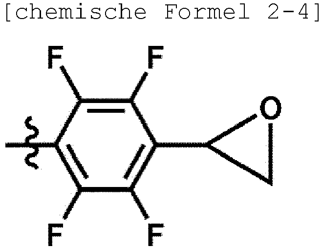
- Chemical Formula 2 is represented by any one of the following Chemical Formulae 2-1 to 2-10.
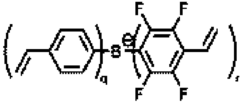
- the anion group of Chemical Formula 1 is any one selected from among the following structural formulae.
- r is an integer of 1 to 4
- q is an integer of 0 to 3
- q+r 4.
- the ionic compound comprises a cation group, wherein the cation group is selected from among monovalent cation groups, onium compounds or the following structural formulae as shown down below.
- the ionic compound includes a cation group, and the cation group is selected from among onium compounds or the following structural formulae.
- the cation group is any one selected from among the following structural formulae. 1-1 1-6 1-2 1-7 1-3 1-8 1-4 1-9 1-5 1-10 1-11 1-12 1-13 1-14 1-15 1-16 1-17 1-18 1-19 3-1 3-3 3-2 4-1 4-3 4-2 5-1 5-4 5-2 5-5 5-3 5-6 6-1 6-3 6-2 6-4
- the ionic compound is selected from among the following structural formulae.
- the present invention provides a coating composition comprising the ionic compound as defined in the claims.
- the coating composition including the ionic compound is a coating composition for an organic light emitting device.
- the coating composition may be a liquid phase.
- the "liquid phase” means in a liquid state at room temperature and atmospheric pressure.
- examples of the solvent may include chlorine-based solvents such as chloroform, methylene chloride, 1,2-dichloroethane, 1,1,2-trichloroethane, chlorobenzene or o-dichlorobenzene; ether-based solvents such as tetrahydrofuran or dioxane; aromatic hydrocarbon-based solvents such as toluene, xylene, trimethylbenzene or mesitylene; aliphatic hydrocarbon-based solvents such as cyclohexane, methylcyclohexane, n-pentane, n-hexane, n-heptane, n-octane, n-nonane or n-decane; ketone-based solvents such as acetone, methyl ethyl ketone or cyclohexanone; ester-based solvents such as ethyl acetate, butyl acetate
- the solvent preferably has a boiling point of 40°C to 250°C, and more preferably 60°C to 230°C, however, the boiling point is not limited thereto.
- the coating composition preferably has a concentration of 0.1 wt/v% to 20 wt/v%, and more preferably 0.5 wt/v% to 5 wt/v%, however, the concentration is not limited thereto.
- thermal polymerization initiator may include peroxides such as methyl ethyl ketone peroxide, methyl isobutyl ketone peroxide, acetylacetone peroxide, methylcyclohexanone peroxide, cyclohexanone peroxide, isobutyryl peroxide, 2,4-dichlorobenzoyl peroxide, bis-3,5,5-trimethyl hexanoyl peroxide, lauryl peroxide, benzoyl peroxide, p-chlorobenzoyl peroxide, dicumyl peroxide, 2,5-dimethyl-2,5-(t-butyloxy)-hexane, 1,3-bis(t-butylperoxy-isopropyl)benzene, t-butyl cumyl peroxide, di-t-butyl peroxide, 2,5-dimethyl-2,5-(di-t-butylperoxy)hexane
- the photopolymerization initiator may include acetophenone-based or ketal-based photopolymerization initiators such as diethoxyacetophenone, 2,2-dimethoxy-1,2-diphenyl ethan-1-one, 1-hydroxy-cyclohexyl-phenyl-ketone, 4-(2-hydroxyethoxy)phenyl-(2-hydroxy-2-propyl)ketone, 2-benzyl-2-dimethylamino-1-(4-morpholinophenyl)butanone-1,2-hydroxy-2-methyl-1-phenylpropan-1-one, 2-methyl-2-morpholino(4-methylthiophenyl)propan-1-one or 1-phenyl-1,2-propanedion-2-(o-ethoxycarbonyl)oxime; benzoin ether-based photopolymerization initiators such as benzoin, benzoin methyl ether, benzoin ethyl ether, benzoin isobutyl ether or benzoin isopropy
- those having a photopolymerization facilitating effect may be used either alone or together with the photopolymerization initiator.
- examples thereof may include triethanolamine, methyldiethanolamine, ethyl 4-dimethylaminobenzoate, isoamyl 4-dimethylaminobenzoate, (2-dimethylamino)ethyl benzoate, 4,4'-dimethylaminobenzophenone and the like, but are not limited thereto.
- Another embodiment of the present specification provides an organic light emitting device formed using the coating composition.
- the organic light emitting device comprises a first electrode; a second electrode provided opposite to the first electrode; and one or more organic material layers provided between the first electrode and the second electrode; wherein one or more layers of the organic material layers include a cured material of the coating composition as defined in the claims.
- the cured material of the coating composition is in a cured state by heat treating or light treating the coating composition.
- the organic material layer including the cured material of the coating composition is a hole injection layer.
- the organic material layer including the cured material of the coating composition is a hole injection layer, and the ionic compound of the cured material of the coating composition is included as a p-doping material of the hole injection layer.
- the organic material layer including the cured material of the coating composition is a hole injection layer, and the ionic compound including the anion group of Chemical Formula 1 is included as a dopant of the hole injection layer.
- the arylamine compound is a monomer or a polymer.
- an arylamine compound that is a monomer or a polymer is further included as a host of the hole injection layer.
- the arylamine compound includes one of the following-structured curing groups.
- L is a direct bond; O; S; a substituted or unsubstituted alkylene group; a substituted or unsubstituted arylene group; or a substituted or unsubstituted divalent heterocyclic group
- k is an integer of 1 or 2, and when k is 2, the Ls are different from each other
- R21 is a substituted or unsubstituted alkyl group, wherein "substituted or unsubstituted” means substituted or unsubstituted with deuterium; a halogen group; an alkyl group; a cycloalkyl group; an alkoxy group; an aryloxy group; an aryl group; an amine group; an arylamine group; and a curing group.
- the host of the hole injection layer has a HOMO level from 4.8 eV to 5.8 eV.
- the compound of the arylamine group forms crosslinking, and an organic material layer including a thin-filmed structure is capable of being provided.
- an organic material layer including a thin-filmed structure is capable of being provided.
- being dissolved by a solvent deposited on a surface of the organic material layer formed using the coating composition, or being morphologically influenced or decomposed may be prevented.
- the organic material layer formed using the coating composition is formed including a step of heat treatment or light treatment, resistance for a solvent increases, and a multilayer may be formed by repeatedly performing solution deposition and crosslinking method, and as a result, a lifetime property of a device may be enhanced due to increased stability.
- the organic material layer formed using the coating composition is a hole transfer layer, a hole injection layer, or a layer carrying out hole transfer and hole injection at the same time.
- the organic material layer formed using the coating composition is a light emitting layer.
- the first electrode is a cathode
- the second electrode is an anode
- the first electrode is an anode
- the second electrode is a cathode
- the organic light emitting device may be an organic light emitting device having a structure in which an anode, one or more organic material layers and a cathode are consecutively laminated on a substrate (normal type).
- the organic light emitting device may be an organic light emitting device having a structure in a reverse direction in which a cathode, one or more organic material layers and an anode are consecutively laminated on a substrate (inverted type).
- the organic material layer of the organic light emitting device of the present specification may be formed in a single layer structure, but may also be formed in a multilayer structure in which two or more organic material layers are laminated.
- the organic light emitting device of the present disclosure may have a structure including a hole injection layer, a hole transfer layer, a light emitting layer, an electron transfer layer, an electron injection layer and the like as the organic material layer.
- the structure of the organic light emitting device is not limited thereto, and may include less numbers of organic material layers.
- FIG. 1 a structure of the organic light emitting device according to one embodiment of the present specification is illustrated in FIG. 1 .
- FIG. 1 illustrates a structure of the organic light emitting device in which an anode (201), a hole injection layer (301), a hole transfer layer (401), a light emitting layer (501), an electron transfer layer (601) and a cathode (701) are consecutively laminated on a substrate (101).
- FIG. 1 illustrates the organic light emitting device, however, the organic light emitting device is not limited thereto.
- the organic material layers may be formed with materials that are the same as or different from each other.
- One embodiment of the present specification also provides a method for manufacturing an organic light emitting device formed using the coating composition.
- the method for manufacturing an organic light emitting device in one embodiment of the present specification includes preparing a substrate; forming a cathode or an anode on the substrate; forming one or more organic material layers on the cathode or the anode; and forming an anode or a cathode on the organic material layers, wherein one or more layers of the organic material layers are formed using the coating composition.
- the organic material layer formed using the coating composition is formed using spin coating.
- the organic material layer formed using the coating composition is formed using a printing method.
- examples of the printing method include inkjet printing, nozzle printing, offset printing, transfer printing, screen printing or the like, but are not limited thereto.
- the coating composition according to one embodiment of the present specification is suited for a solution process due to its structural properties and may be formed using a printing method, and therefore, is economically effective in terms of time and costs when manufacturing a device.
- the time of heat treating the organic material layer formed using the coating composition is preferably within 1 hour and more preferably within 30 minutes.
- composition according to one embodiment of the present specification may be thin-filmed through heat treatment or light treatment, and may be included as a copolymer using a coating composition mixed with other monomers.
- a copolymer or a mixture may be included using a coating composition mixed with other polymers.
- the cathode material materials having small work function are normally preferred so that electron injection to an organic material layer is smooth.
- the cathode material include metals such as magnesium, calcium, sodium, potassium, titanium, indium, yttrium, lithium, gadolinium, aluminum, silver, tin and lead, or alloys thereof; multilayer structure materials such as LiF/Al or LiO 2 /Al, and the like, but are not limited thereto.
- the hole injection layer is a layer that injects holes from an electrode
- the hole injection material is preferably a compound that has an ability to transfer holes, therefore, has a hole injection effect in an anode, has an excellent hole injection effect for a light emitting layer or a light emitting material, prevents excitons generated in the light emitting layer from moving to an electron injection layer or an electron injection material, and in addition, has an excellent thin film forming ability.
- the highest occupied molecular orbital (HOMO) of the hole injection material is preferably in between the work function of an anode material and the HOMO of surrounding organic material layers.
- the hole injection material examples include metal porphyrins, oligothiophene, arylamine-based organic materials, hexanitrile hexaazatriphenylene-based organic materials, quinacridone-based organic materials, perylene-based organic materials, anthraquinone, and polyaniline- and polythiophene-based conductive polymers, and the like, but are not limited thereto.
- the hole transfer layer is a layer that receives holes from a hole injection layer and transfers the holes to a light emitting layer
- the hole transfer material materials capable of receiving holes from an anode or a hole injection layer, moving the holes to a light emitting layer, and having high mobility for the holes are suitable.
- Specific examples thereof include arylamine-based organic materials, conductive polymers, block copolymers having conjugated parts and nonconjugated parts together, and the like, but are not limited thereto.
- the light emitting material is a material capable of emitting light in a visible light region by receiving holes and electrons from a hole transfer layer and an electron transfer layer, respectively, and binding the holes and the electrons, and is preferably a material having favorable quantum efficiency for fluorescence or phosphorescence.
- Specific examples thereof include 8-hydroxyquinoline aluminum complexes (Alq 3 ) ; carbazole-based compounds; dimerized styryl compounds; BAlq; 10-hydroxybenzo quinoline-metal compounds; benzoxazole-, benzthiazole- and benzimidazole-based compounds; poly(p-phenylenevinylene) (PPV)-based polymers; spiro compounds; polyfluorene, rubrene, and the like, but are not limited thereto.
- Alq 3 8-hydroxyquinoline aluminum complexes
- carbazole-based compounds dimerized styryl compounds
- BAlq 10-hydroxybenzo quinoline-metal compounds
- benzoxazole-, benzthiazole- and benzimidazole-based compounds benzoxazole-, benzthiazole- and benzimidazole-based compounds
- PV poly(p-phenylenevinylene)
- the light emitting layer may include a host material and a dopant material.
- the host material includes fused aromatic ring derivatives, heteroring-containing compounds or the like.
- the fused aromatic ring derivative includes anthracene derivatives, pyrene derivatives, naphthalene derivatives, pentacene derivatives, phenanthrene compounds, fluoranthene compounds and the like
- the heteroring-containing compound includes carbazole derivatives, dibenzofuran derivatives, ladder-type furan compounds, pyrimidine derivatives and the like, however, the material is not limited thereto.
- the dopant material includes aromatic amine derivatives, styrylamine compounds, boron complexes, fluoranthene compounds, metal complexes and the like.
- the aromatic amine derivative is a fused aromatic ring derivative having a substituted or unsubstituted arylamino group and includes arylamino group-including pyrene, anthracene, chrysene, peryflanthene and the like
- the styrylamine compound is a compound in which substituted or unsubstituted arylamine is substituted with at least one arylvinyl group, and one, two or more substituents selected from the group consisting of an aryl group, a silyl group, an alkyl group, a cycloalkyl group and an arylamino group are substituted or unsubstituted.
- styrylamine styryldiamine, styryltriamine, styryltetramine or the like is included, however, the styrylamine compound is not limited thereto.
- the metal complex includes iridium complexes, platinum complexes or the like, but is not limited thereto.
- the hole blocking layer is a layer blocking holes from reaching a cathode, and generally, may be formed under the same condition as the hole injection layer. Specifically, oxadiazole derivatives or triazole derivatives, phenanthroline derivatives, BCP, aluminum complexes and the like are included, however, the material is not limited thereto.
- the organic light emitting device may be a top-emission type, a bottom-emission type or a dual-emission type depending on the materials used.
- the coating composition may be included in organic solar cells or organic transistors in addition to organic light emitting devices.
- the synthesized material was extracted using EA (3x10 mL), and residual water was removed with MgSO 4 . After removing all the solvent, water was completely removed with Dean-stark using benzene, and the solids were filtered to obtain a target compound (400 mg). (Yield: 62%)
- the DSC data are differential scanning calorimeter data, and curing of the dopant material was seen through FIG. 3 .
- Coating Composition 1 was produced by mixing a p-doping material represented by the following Compound 1, a host compound that is the following [Compound A], and an organic solvent (cyclohexanone). Specifically, Compound 1, Compound A and the organic solvent were mixed in a weight ratio of 2:8:490 to produce the coating composition, and Coating Composition 1 was spin coated to form a coating layer, and the film was baked at 250°C or lower.
- Coating Composition 2 was produced in the same manner as Coating Composition 1 except that the following Compound 2 was used instead of Compound 1 of the present disclosure. Coating Composition 2 was spin coated to form a coating layer, and the film was baked at 250°C or lower.
- Coating Composition 3 was produced in the same manner as Coating Composition 1 except that the following Compound 3 was used instead of Compound 1 of the present disclosure. Coating Composition 3 was spin coated to form a coating layer, and the film was baked at 250°C or lower.
- Coating Composition 4 was produced in the same manner as Coating Composition 1 except that the following Compound 4 was used instead of Compound 1 of the present disclosure. Coating Composition 4 was spin coated to form a coating layer, and the film was baked at 250°C or lower.
- Coating Composition 6 was produced in the same manner as Coating Composition 4 except that the following [Compound C] was used instead of [Compound A] of the present disclosure. Coating Composition 6 was spin coated to form a coating layer, and the film was baked at 250°C or lower.
- Coating Composition 7 was produced in the same manner as Coating Composition 1 except that the following Compound 7 was used instead of Compound 1 of the present disclosure. Coating Composition 7 was spin coated to form a coating layer, and the film was baked at 250°C or lower.
- Coating Composition 8 was produced in the same manner as Coating Composition 1 except that the following Comparative Compound 1 was used instead of Compound 1 of the present disclosure. Coating Composition 8 was spin coated to form a coating layer, and the film was baked at 250°C or lower.
- Coating Composition 9 was produced in the same manner as Coating Composition 1 except that the following Comparative Compound 2 was used instead of Compound 1 of the present disclosure. Coating Composition 9 was spin coated to form a coating layer, and the film was baked at 250°C or lower.
- Coating Composition 4 was spin coated for 60 seconds at a spin rate of 1000 rpm, and then baked through heating for 30 minutes on a hot plate at 230°C to form a thin film. The result was immersed for 10 minutes in toluene, taken out, and the film retention rate was measured using UV-Visible spectroscopy and shown in FIG. 6 .
- FIG. 6 shows film retention rate data of Coating Composition 4.
- the film retention rate was measured in the same manner except that Coating Composition 8 was used instead of Coating Composition 4, and shown in FIG. 7.
- FIG. 7 shows film retention rate data of Coating Composition 8.
- FIG. 8 shows film retention rate data of Coating Composition 9.
- the film retention rate data were obtained by comparing the degree of ultraviolet absorbance before and after the process of forming the film described above.
- Coating Composition 1 described in the table was spin coated to form a hole injection layer having a thickness of 300 ⁇ , and the coating composition was cured for 30 minutes on a hot plate under N 2 atmosphere. After that, the result was transferred to a vacuum depositor, and then Compound D was vacuum deposited on the hole injection layer to form a hole transfer layer.
- a light emitting layer was formed on the hole transfer layer by vacuum depositing Compound F in a concentration of 8% with respect to Compound E to a thickness of 300 ⁇ .
- Compound G was vacuum deposited to a thickness of 200 ⁇ to form an electron injection and transfer layer.
- a cathode was formed on the electron injection and transfer layer by depositing LiF to a thickness of 12 ⁇ and aluminum to a thickness of 2,000 ⁇ in consecutive order.
- An organic light emitting device was manufactured in the same manner as in Example 1 except that Coating Composition 2 was used instead of Coating Composition 1 as the hole injection layer.
- An organic light emitting device was manufactured in the same manner as in Example 1 except that Coating Composition 3 was used instead of Coating Composition 1 as the hole injection layer.
- An organic light emitting device was manufactured in the same manner as in Example 1 except that Coating Composition 4 was used instead of Coating Composition 1 as the hole injection layer.
- An organic light emitting device was manufactured in the same manner as in Example 1 except that Coating Composition 5 was used instead of Coating Composition 1 as the hole injection layer.
- An organic light emitting device was manufactured in the same manner as in Example 1 except that Coating Composition 7 was used instead of Coating Composition 1 as the hole injection layer.
- An organic light emitting device was manufactured in the same manner as in Example 1 except that Coating Composition 8 was used instead of Coating Composition 1 as the hole injection layer.
- the dopant having the structure of Chemical Formula 1 of the present specification had superior solubility for an organic solvent compared to generally-used dopants, and was thereby suited for solution processes, and, since a coating composition was readily prepared, a uniform coating layer may be formed using the coating composition.
- a curing group was present preventing a lifetime decrease caused by interlayer inflow, and therefore, the dopant was able to be used in an organic light emitting device.
Landscapes
- Chemical & Material Sciences (AREA)
- Organic Chemistry (AREA)
- Engineering & Computer Science (AREA)
- Materials Engineering (AREA)
- Physics & Mathematics (AREA)
- Spectroscopy & Molecular Physics (AREA)
- Health & Medical Sciences (AREA)
- Chemical Kinetics & Catalysis (AREA)
- Medicinal Chemistry (AREA)
- Polymers & Plastics (AREA)
- Optics & Photonics (AREA)
- Wood Science & Technology (AREA)
- Life Sciences & Earth Sciences (AREA)
- Inorganic Chemistry (AREA)
- Manufacturing & Machinery (AREA)
- Electroluminescent Light Sources (AREA)
- Organic Low-Molecular-Weight Compounds And Preparation Thereof (AREA)
- Paints Or Removers (AREA)
- Quinoline Compounds (AREA)
- Pyridine Compounds (AREA)
- Pyrane Compounds (AREA)
- Polyoxymethylene Polymers And Polymers With Carbon-To-Carbon Bonds (AREA)
- Addition Polymer Or Copolymer, Post-Treatments, Or Chemical Modifications (AREA)
Claims (14)
- Ionische Verbindung, umfassend eine Anionengruppe, dargestellt durch die folgende chemische Formel 1:


die verbliebenen R1 bis R5, falls vorhanden, gleich oder unterschiedlich, und jeweils unabhängig Wasserstoff; Deuterium; eine Nitrogruppe; -C(O)R100; - OR101; -SR102; -SO3R103; -COOR104; -OC(O)R105; -C(O)NR106R107; eine Alkylgruppe; eine Alkenylgruppe; eine Alkynylgruppe; eine Amingruppe; eine Arylgruppe; oder eine heterocyclische Gruppe sind;
R100 bis R107 gleich oder unterschiedlich, und jeweils unabhängig Wasserstoff; Deuterium; oder eine Alkylgruppe sind,
die verbliebenen R6 bis R10, falls vorhanden, gleich oder unterschiedlich, und jeweils unabhängig Wasserstoff; Deuterium; eine Nitrogruppe; -C(O)R100; - OR101; -SR102; -SO3R103; -COOR104; -OC(O)R105; -C(O)NR106R107; eine Alkylgruppe; eine Fluoralkylgruppe; eine Alkenylgruppe; eine Alkynylgruppe; eine Amingruppe; eine Arylgruppe; oder eine heterocyclische Gruppe sind; und
R100 bis R107 gleich oder unterschiedlich, und jeweils unabhängig Wasserstoff; Deuterium; oder eine Alkylgruppe sind;
worin die härtende Gruppe ausgewählt ist aus der Gruppe, bestehend aus den folgenden härtenden Gruppen: [Gruppe der härtenden Gruppen]

- Ionische Verbindung gemäß Anspruch 1, worin die chemische Formel 2 dargestellt wird durch eine beliebige der folgenden chemischen Formeln 2-1 bis 2-10:




- Ionische Verbindung gemäß Anspruch 1, worin die chemische Formel 3 dargestellt wird durch eine beliebige der folgenden chemischen Formeln 3-1 bis 3-8:


- Ionische Verbindung gemäß Anspruch 1, worin die Anionengruppe der chemischen Formel 1 eine beliebige ist, ausgewählt aus den folgenden Strukturformeln:


- Ionische Verbindung gemäß Anspruch 1, umfassend eine Kationengruppe, worin die Kationengruppe ausgewählt ist aus monovalenten Kationengruppen, Oniumverbindungen oder den folgenden Strukturformeln:

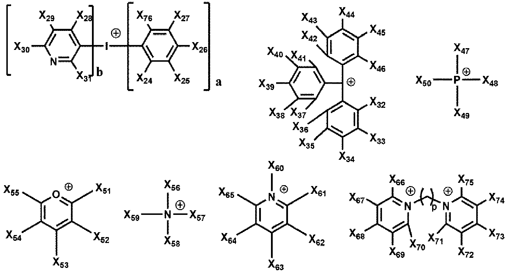
R104 Wasserstoff; Deuterium; eine substituierte oder eine unsubstituierte Alkylgruppe ist;
p eine ganze Zahl aus 0 bis 10 ist; und
a 1 oder 2 ist, b 0 oder 1 ist, und a+b=2,
worin "substituiert oder unsubstituiert" bedeutet: substituiert oder unsubstituiert mit Deuterium; einer Halogengruppe; einer Alkylgruppe; einer Cycloalkylgruppe; einer Alkoxygruppe; einer Aryloxygruppe; einer Arylgruppe; einer Amingruppe; einer Arylamingruppe; und einer härtenden Gruppe. - Ionische Verbindung gemäß Anspruch 5, worin die Kationengruppe dargestellt wird durch eine beliebige der folgenden chemischen Formeln 10 bis 15:


R104 eine substituierte oder unsubstituierte Alkylgruppe ist, worin "substituiert oder unsubstituiert" bedeutet: substituiert oder unsubstituiert mit Deuterium; einer Halogengruppe; einer Alkylgruppe; einer Cycloalkylgruppe; einer Alkoxygruppe; einer Aryloxygruppe; einer Arylgruppe; einer Amingruppe; einer Arylamingruppe; und einer härtenden Gruppe. - Ionische Verbindung gemäß Anspruch 5, worin die Kationengruppe eine beliebige ist, ausgewählt aus den folgenden Strukturformeln:
1-1 
1-6 
1-2 
1-7 
1-3 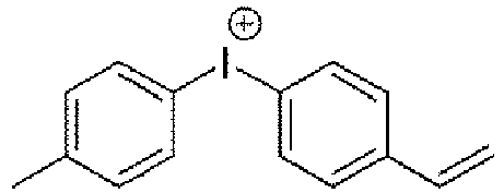
1-8 
1-4 
1-9 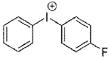
1-5 
1-10 
1-11 
1-12 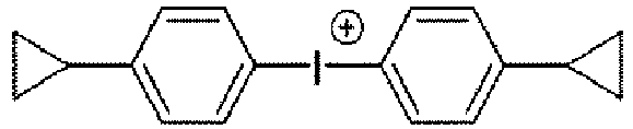
1-13 
1-14 
1-15 
1-16 
1-17 
1-18 
1-19 
3-1 
3-3 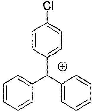
3-2 
4-1 
4-3 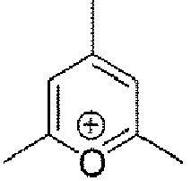
4-2 
5-1 
5-4 
5-2 
5-5 
5-3 
5-6 
6-1 
6-3 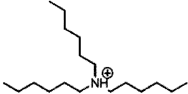
6-2 
6-4 
- Ionische Verbindung gemäß Anspruch 1, die ausgewählt ist aus den folgenden Strukturformeln:


- Beschichtungszusammensetzung, umfassend die ionische Verbindung gemäß einem beliebigen der Ansprüche 1 bis 8.
- Beschichtungszusammensetzung gemäß Anspruch 9, ferner umfassend eine Arylaminverbindung, die ein Monomer oder ein Polymer ist.
- Beschichtungszusammensetzung gemäß Anspruch 10, worin die Arylaminverbindung mindestens eine der folgenden strukturierten härtenden Gruppen einschließt:


k eine ganze Zahl aus 1 oder 2 ist, und wenn k 2 ist, die Ls unterschiedlich sind, und R21 eine substituierte oder unsubstituierte Alkylgruppe ist,
worin "substituiert oder unsubstituiert" bedeutet: substituiert oder unsubstituiert mit Deuterium; einer Halogengruppe; einer Alkylgruppe; einer Cycloalkylgruppe; einer Alkoxygruppe; einer Aryloxygruppe; einer Arylgruppe; einer Amingruppe; einer Arylamingruppe; und einer härtenden Gruppe. - Organische lichtemittierende Vorrichtung, umfassend:eine erste Elektrode;eine zweite Elektrode, die gegenüber der ersten Elektrode vorgesehen ist; undeine oder mehrere Schichten aus organischem Material, die zwischen der ersten Elektrode und der zweiten Elektrode vorgesehen sind, worin eine oder mehrere Schichten der organischen Materialschichten ein gehärtetes Material der Beschichtungszusammensetzung gemäß Anspruch 9 enthalten.
- Organische lichtemittierende Vorrichtung gemäß Anspruch 12, worin das gehärtete Material der Beschichtungszusammensetzung durch Wärmebehandlung oder Lichtbehandlung der Beschichtungszusammensetzung in einen gehärteten Zustand gebracht wurde.
- Organische lichtemittierende Vorrichtung gemäß Anspruch 12, worin die organische Materialschicht, die das gehärtete Material der Beschichtungszusammensetzung enthält, eine Defektelektrontransportschicht, eine Defektelektroninjektionsschicht oder eine Schicht, die gleichzeitig Defektelektrontransport und Defektelektroninjektion durchführt, ist.
Applications Claiming Priority (2)
| Application Number | Priority Date | Filing Date | Title |
|---|---|---|---|
| KR20160158461 | 2016-11-25 | ||
| PCT/KR2017/013549 WO2018097659A1 (ko) | 2016-11-25 | 2017-11-24 | 이온성 화합물, 이를 포함하는 코팅 조성물 및 유기 발광 소자 |
Publications (3)
| Publication Number | Publication Date |
|---|---|
| EP3524646A1 EP3524646A1 (de) | 2019-08-14 |
| EP3524646A4 EP3524646A4 (de) | 2019-11-13 |
| EP3524646B1 true EP3524646B1 (de) | 2021-07-21 |
Family
ID=62195244
Family Applications (4)
| Application Number | Title | Priority Date | Filing Date |
|---|---|---|---|
| EP17874741.6A Active EP3511382B1 (de) | 2016-11-25 | 2017-11-24 | Organische lichtemittierende diode |
| EP17874046.0A Active EP3540015B1 (de) | 2016-11-25 | 2017-11-24 | Verwendung einer beschichtungszusammensetzung und organische lichtemittierende vorrichtung |
| EP17874454.6A Active EP3524646B1 (de) | 2016-11-25 | 2017-11-24 | Ionische verbindung, beschichtungszusammensetzung damit und organische lichtemittierende diode |
| EP17872963.8A Active EP3521384B1 (de) | 2016-11-25 | 2017-11-24 | Ionische verbindung und beschichtungszusammensetzung sowie organische lichtemittierende vorrichtung damit |
Family Applications Before (2)
| Application Number | Title | Priority Date | Filing Date |
|---|---|---|---|
| EP17874741.6A Active EP3511382B1 (de) | 2016-11-25 | 2017-11-24 | Organische lichtemittierende diode |
| EP17874046.0A Active EP3540015B1 (de) | 2016-11-25 | 2017-11-24 | Verwendung einer beschichtungszusammensetzung und organische lichtemittierende vorrichtung |
Family Applications After (1)
| Application Number | Title | Priority Date | Filing Date |
|---|---|---|---|
| EP17872963.8A Active EP3521384B1 (de) | 2016-11-25 | 2017-11-24 | Ionische verbindung und beschichtungszusammensetzung sowie organische lichtemittierende vorrichtung damit |
Country Status (7)
| Country | Link |
|---|---|
| US (4) | US11165037B2 (de) |
| EP (4) | EP3511382B1 (de) |
| JP (4) | JP6749676B2 (de) |
| KR (4) | KR101948183B1 (de) |
| CN (4) | CN109804027B (de) |
| TW (3) | TWI642675B (de) |
| WO (4) | WO2018097661A1 (de) |
Families Citing this family (34)
| Publication number | Priority date | Publication date | Assignee | Title |
|---|---|---|---|---|
| KR102126602B1 (ko) * | 2016-04-22 | 2020-06-24 | 주식회사 엘지화학 | 카바졸 유도체 및 이를 이용한 유기 발광 소자 |
| CN109804027B (zh) | 2016-11-25 | 2022-03-01 | 株式会社Lg化学 | 离子化合物、包含其的涂覆组合物和有机发光二极管 |
| CN111164113B (zh) | 2018-02-28 | 2022-10-11 | 株式会社Lg化学 | 聚合物、包含其的涂覆组合物和使用其的有机发光元件 |
| WO2019225987A1 (ko) * | 2018-05-23 | 2019-11-28 | 주식회사 엘지화학 | 화합물, 이를 포함하는 코팅 조성물 및 유기 발광 소자 |
| KR102496107B1 (ko) * | 2018-07-03 | 2023-02-03 | 주식회사 엘지화학 | 이온성 화합물, 이를 포함하는 코팅 조성물 및 유기 발광 소자 |
| CN108795420A (zh) * | 2018-07-17 | 2018-11-13 | 深圳市华星光电技术有限公司 | Oled电致发光材料及其制备方法、oled显示面板 |
| KR102316066B1 (ko) | 2018-07-27 | 2021-10-21 | 주식회사 엘지화학 | 잉크 조성물, 이를 이용한 유기 발광 소자 및 이의 제조방법 |
| KR102153086B1 (ko) | 2018-07-31 | 2020-09-07 | 주식회사 엘지화학 | 신규한 고분자 및 이를 포함하는 유기 발광 소자 |
| KR102576153B1 (ko) * | 2018-09-21 | 2023-09-06 | 주식회사 엘지화학 | 신규한 공중합체 및 이를 포함하는 유기 발광 소자 |
| JP7275738B2 (ja) * | 2018-09-21 | 2023-05-18 | 三菱ケミカル株式会社 | 組成物、電荷輸送膜及び有機電界発光素子 |
| WO2020075014A1 (en) * | 2018-10-10 | 2020-04-16 | Semiconductor Energy Laboratory Co., Ltd. | Light-emitting device, light-emitting apparatus, electronic device, and lighting device |
| KR102764481B1 (ko) * | 2018-11-15 | 2025-02-05 | 주식회사 엘지화학 | 신규한 고분자 및 이를 이용한 유기발광 소자 |
| KR102252886B1 (ko) * | 2018-11-27 | 2021-05-17 | 주식회사 엘지화학 | 신규한 고분자 및 이를 이용한 유기발광 소자 |
| WO2020111603A1 (ko) * | 2018-11-27 | 2020-06-04 | 주식회사 엘지화학 | 신규한 고분자 및 이를 이용한 유기발광 소자 |
| KR102696401B1 (ko) * | 2019-03-27 | 2024-08-16 | 주식회사 엘지화학 | 유기 발광 소자의 정공 주입층 제조용 조성물 |
| CN113906577B (zh) * | 2019-08-23 | 2025-02-21 | 株式会社Lg化学 | 有机发光器件 |
| CN113841265B (zh) * | 2019-08-26 | 2023-09-22 | 株式会社Lg化学 | 有机发光器件 |
| US20230006159A1 (en) * | 2019-09-06 | 2023-01-05 | Nippon Hoso Kyokai | Organic thin film, method for producing organic thin film, organic electroluminescent element, display device, lighting device, organic thin film solar cell, thin film transistor, photoelectric conversion element, coating composition and material for organic electroluminescent elements |
| KR102799972B1 (ko) * | 2019-09-09 | 2025-04-23 | 주식회사 엘지화학 | 잉크 조성물, 이를 이용한 유기 발광 소자 및 이의 제조방법 |
| KR102678173B1 (ko) * | 2019-11-07 | 2024-06-26 | 주식회사 엘지화학 | 양자점 발광 소자 및 이를 포함하는 표시 장치 |
| KR102845761B1 (ko) * | 2020-01-08 | 2025-08-12 | 주식회사 엘지화학 | 중합체, 이를 포함하는 코팅 조성물 및 이를 이용한 유기 발광 소자 |
| CN111518280B (zh) * | 2020-04-30 | 2022-04-08 | 广州市浪奇实业股份有限公司 | 一种改性纤维素及其应用 |
| CN111518233B (zh) * | 2020-04-30 | 2022-04-29 | 广州市浪奇实业股份有限公司 | 一种阳离子表面活性剂的制备方法及其应用 |
| EP4145546B1 (de) * | 2020-08-06 | 2025-01-29 | Lg Chem, Ltd. | Organische lichtemittierende vorrichtung |
| JP7682928B2 (ja) * | 2020-08-06 | 2025-05-26 | エルジー・ケム・リミテッド | 有機発光素子 |
| KR102680194B1 (ko) | 2020-09-10 | 2024-07-01 | 주식회사 엘지화학 | 유기 발광 소자 |
| CN114335363B (zh) * | 2020-09-30 | 2024-01-30 | 江苏三月科技股份有限公司 | 一种有机电致发光器件用组合物及有机电致发光器件 |
| KR102903875B1 (ko) * | 2020-10-29 | 2025-12-23 | 주식회사 엘지화학 | 유기 발광 소자 |
| TW202242069A (zh) * | 2020-12-23 | 2022-11-01 | 日商三菱化學股份有限公司 | 有機電場發光元件、有機el顯示裝置、有機el照明及有機電場發光元件的製造方法 |
| US20240279249A1 (en) * | 2021-03-25 | 2024-08-22 | Lg Chem, Ltd. | Compound, Coating Composition Comprising Same, Organic Light-Emitting Device Using Same, and Manufacturing Method Therefor |
| JP2022164474A (ja) * | 2021-04-16 | 2022-10-27 | 三菱ケミカル株式会社 | 量子ドット発光素子、量子ドット表示装置、量子ドット照明及び量子ドット発光素子の製造方法 |
| JP2022164473A (ja) * | 2021-04-16 | 2022-10-27 | 三菱ケミカル株式会社 | 量子ドット発光素子、量子ドット表示装置、量子ドット照明及び量子ドット発光素子の製造方法 |
| JPWO2023189861A1 (de) * | 2022-03-29 | 2023-10-05 | ||
| CN116786160B (zh) * | 2023-05-25 | 2025-05-23 | 浙江理工大学嵊州创新研究院有限公司 | 一种含氟离子液体催化剂的制备及其在高效co2转化中的应用 |
Citations (2)
| Publication number | Priority date | Publication date | Assignee | Title |
|---|---|---|---|---|
| JP2016060764A (ja) * | 2014-09-16 | 2016-04-25 | 株式会社日本触媒 | ポリアクリル酸(塩)系吸水性樹脂の製造方法 |
| EP3540015A2 (de) * | 2016-11-25 | 2019-09-18 | LG Chem, Ltd. | Beschichtungszusammensetzung und organische lichtemittierende vorrichtung |
Family Cites Families (53)
| Publication number | Priority date | Publication date | Assignee | Title |
|---|---|---|---|---|
| JP3273944B2 (ja) | 1991-11-25 | 2002-04-15 | エクソンモービル・ケミカル・パテンツ・インク | ポリアニオン性遷移金属触媒組成物 |
| JPH08127611A (ja) * | 1994-11-01 | 1996-05-21 | Showa Denko Kk | ホウ素含有化合物 |
| EP0710663A1 (de) * | 1994-11-01 | 1996-05-08 | Japan Polyolefins Co., Ltd. | Borenthaltende Verbindung, sein Polymer, diese Polymer und ein Metallocen enthaltender Katalysator und ein Verfahren zur Herstellung eines Polyolefins |
| JPH08143617A (ja) | 1994-11-24 | 1996-06-04 | Showa Denko Kk | 重合触媒及びポリオレフィンの製造方法 |
| DE19613650C1 (de) * | 1996-04-04 | 1997-04-10 | Fraunhofer Ges Forschung | Hydrolisierbare, fluorierte Silane, Verfahren zu deren Herstellung und deren Verwendung zur Herstellung von Kieselsäurepolykondensaten und Kieselsäureheteropolykondensaten |
| JPH11286491A (ja) | 1998-03-31 | 1999-10-19 | Idemitsu Petrochem Co Ltd | イオン性化合物、オレフィン重合用触媒およびオレフィン系重合体の製造方法 |
| JP2000178281A (ja) | 1998-12-18 | 2000-06-27 | Idemitsu Petrochem Co Ltd | イオン性化合物、オレフィン類重合用触媒及びオレフィン系重合体の製造方法 |
| US6465385B1 (en) | 1999-02-12 | 2002-10-15 | Sunoco, Inc. (R&M) | Zwitterionic polymerization catalyst |
| AU2001264832A1 (en) * | 2000-05-23 | 2001-12-03 | Aprilis, Inc. | Data storage medium comprising colloidal metal and preparation process thereof |
| EP1217668A1 (de) | 2000-12-22 | 2002-06-26 | Covion Organic Semiconductors GmbH | Verwendung von Bor- und Aluminium-Verbindungen in Elektronik-Bauteilen |
| US7521168B2 (en) * | 2002-02-13 | 2009-04-21 | Fujifilm Corporation | Resist composition for electron beam, EUV or X-ray |
| EP2265092B1 (de) * | 2002-06-06 | 2018-03-14 | UDC Ireland Limited | Elektrolumineszierende Vorrichtung |
| US20070020479A1 (en) | 2003-05-12 | 2007-01-25 | Yasunori Uetani | Luminescent-polymer composition |
| EP2918590A1 (de) * | 2004-03-11 | 2015-09-16 | Mitsubishi Chemical Corporation | Zusammensetzung für eine ladungstransportfolie und ionenzusammensetzung, ladetransportfolie und organische elektrolumineszenzvorrichtung damit, und herstellungsverfahren der organischen elektrolumineszenzvorrichtung und herstellungsverfahren der ladungstransportfolie |
| CN100486396C (zh) * | 2004-03-11 | 2009-05-06 | 三菱化学株式会社 | 电荷输送膜用组合物和离子化合物、电荷输送膜和有机电致发光器件及其制造方法 |
| JP4692025B2 (ja) * | 2004-03-11 | 2011-06-01 | 三菱化学株式会社 | 電荷輸送膜用組成物及びイオン化合物、それを用いた電荷輸送膜及び有機電界発光素子、並びに、有機電界発光素子の製造方法及び電荷輸送膜の製造方法 |
| EP1887640A4 (de) | 2005-05-24 | 2012-04-04 | Pioneer Corp | Organisches elektrolumineszenzbauelement |
| US8222632B2 (en) * | 2005-06-22 | 2012-07-17 | Sumitomo Chemical Company, Limited | Polymeric material and polymeric luminescent element |
| JP4931827B2 (ja) | 2005-12-16 | 2012-05-16 | パイオニア株式会社 | 有機エレクトロルミネッセンス素子 |
| JP2008063329A (ja) | 2006-08-08 | 2008-03-21 | Koei Chem Co Ltd | アンモニウム塩 |
| CN101842409B (zh) * | 2007-11-01 | 2013-05-01 | 株式会社Adeka | 盐化合物、阳离子聚合引发剂及阳离子聚合性组合物 |
| JP5434088B2 (ja) * | 2008-01-22 | 2014-03-05 | 三菱化学株式会社 | 架橋性有機化合物、有機電界発光素子用組成物、有機電界発光素子および有機elディスプレイ |
| EP2291872A1 (de) | 2008-06-27 | 2011-03-09 | Universal Display Corporation | Vernetzbare ionische dotierungsstoffe |
| JP4991648B2 (ja) | 2008-06-30 | 2012-08-01 | 積水化学工業株式会社 | 有機エレクトロルミネッセンス素子封止剤 |
| KR101762964B1 (ko) | 2008-10-27 | 2017-07-28 | 닛산 가가쿠 고교 가부시키 가이샤 | 전하 주입 및 수송 층 |
| JP5884213B2 (ja) | 2009-03-13 | 2016-03-15 | 三菱化学株式会社 | 有機電界発光素子の製造方法、有機電界発光素子、有機elディスプレイ及び有機el照明 |
| JP5696662B2 (ja) * | 2009-06-01 | 2015-04-08 | 日立化成株式会社 | 有機エレクトロルミネセンス素子、表示素子、照明装置および表示装置 |
| KR101231931B1 (ko) * | 2009-11-13 | 2013-02-08 | 주식회사 엘지화학 | 신규한 축합고리 화합물 및 이를 이용한 유기전자소자 |
| TWI440238B (zh) | 2010-03-22 | 2014-06-01 | 國立成功大學 | 以四級va族離子型有機鹽類作為電子傳輸層的有機光電半導體元件及其製造方法 |
| EP2588527B1 (de) | 2010-07-02 | 2017-10-25 | Nissan Chemical Industries, Ltd. | Lochtranportzusammensetzungen, zugehörige vorrichtungen und verfahren (i) |
| KR101906284B1 (ko) | 2010-07-30 | 2018-10-11 | 고쿠리쓰다이가쿠호진 규슈다이가쿠 | 유기전계발광소자 |
| JP5918236B2 (ja) | 2010-08-20 | 2016-05-18 | ロディア オペレーションズRhodia Operations | ポリマー組成物、ポリマーフィルム、ポリマーゲル、ポリマーフォーム、並びに当該フィルム、ゲル及びフォームを含有する電子デバイス |
| KR101463298B1 (ko) | 2011-04-01 | 2014-11-20 | 주식회사 엘지화학 | 새로운 유기 발광 소자 재료 및 이를 이용한 유기 발광 소자 |
| JP2013095820A (ja) * | 2011-10-31 | 2013-05-20 | Fujifilm Corp | 導電性組成物、並びにこれを用いた導電性膜及び導電性積層体 |
| JP2013170223A (ja) * | 2012-02-21 | 2013-09-02 | Sekisui Chem Co Ltd | 蒸着用硬化性樹脂組成物、樹脂保護膜、及び、有機光デバイス |
| JP6432347B2 (ja) | 2012-05-28 | 2018-12-05 | 三菱ケミカル株式会社 | 導電性薄膜積層体の製造方法 |
| EP2750215B1 (de) * | 2012-07-18 | 2016-10-26 | LG Display Co., Ltd. | Organische lichtemittierende vorrichtung |
| WO2014038559A1 (ja) | 2012-09-04 | 2014-03-13 | 三菱化学株式会社 | 有機電界発光素子及びその製造方法 |
| CN103865220A (zh) | 2012-11-16 | 2014-06-18 | 陶氏环球技术有限责任公司 | 有机金属聚合物组合物,制备它的方法,和由其制造的有机发光二极管 |
| WO2014075298A1 (en) * | 2012-11-16 | 2014-05-22 | Dow Global Technologies Llc | Organometallic polymer composition, process for preparing the same, and oled fabricated therefrom |
| JP5830041B2 (ja) | 2013-01-24 | 2015-12-09 | 信越化学工業株式会社 | ポリシロキサン含有レジスト下層膜形成用組成物、及びこれを用いたパターン形成方法 |
| US10665786B2 (en) | 2013-03-08 | 2020-05-26 | Hitachi Chemical Company, Ltd. | Treatment liquid containing ionic compound, organic electronic element, and method for producing organic electronic element |
| JP6240409B2 (ja) * | 2013-05-31 | 2017-11-29 | サンアプロ株式会社 | スルホニウム塩および光酸発生剤 |
| JP6018984B2 (ja) * | 2013-07-31 | 2016-11-02 | 富士フイルム株式会社 | 着色組成物、硬化膜、カラーフィルタ、カラーフィルタの製造方法、固体撮像素子および画像表示装置 |
| KR102117603B1 (ko) * | 2014-02-10 | 2020-06-01 | 덕산네오룩스 주식회사 | 유기전기소자용 화합물, 이를 이용한 유기전기소자 및 그 전자 장치 |
| KR102250691B1 (ko) * | 2014-10-06 | 2021-05-13 | 덕산네오룩스 주식회사 | 유기전기 소자용 화합물, 이를 이용한 유기전기소자 및 그 전자 장치 |
| KR102554985B1 (ko) | 2015-01-16 | 2023-07-12 | 도오꾜오까고오교 가부시끼가이샤 | 레지스트 조성물 및 레지스트 패턴 형성 방법 |
| KR102408598B1 (ko) | 2015-03-31 | 2022-06-14 | 스미또모 가가꾸 가부시키가이샤 | 점착제층 부착 광학 필름 및 액정 표시 장치 |
| KR102656454B1 (ko) * | 2016-03-03 | 2024-04-12 | 닛산 가가쿠 가부시키가이샤 | 전하 수송성 바니시 |
| WO2017164268A1 (ja) * | 2016-03-24 | 2017-09-28 | 三菱化学株式会社 | 電子受容性化合物及び電荷輸送膜用組成物、それを用いた発光素子 |
| ES2969779T3 (es) | 2016-04-15 | 2024-05-22 | Becton Dickinson Co | Clasificador de gotículas cerrado, métodos de uso del mismo y kit |
| EP3463245B1 (de) | 2016-05-31 | 2021-10-20 | Koninklijke Philips N.V. | Schälkopf mit wälzkörpern |
| MX2020005067A (es) | 2017-11-15 | 2020-08-20 | Otto Ladder Safety Inc | Escalera que tiene sensor y dispositivo de computo para el mismo. |
-
2017
- 2017-11-24 CN CN201780063027.7A patent/CN109804027B/zh active Active
- 2017-11-24 TW TW106140975A patent/TWI642675B/zh active
- 2017-11-24 US US16/335,965 patent/US11165037B2/en active Active
- 2017-11-24 US US16/334,537 patent/US11765921B2/en active Active
- 2017-11-24 JP JP2019520122A patent/JP6749676B2/ja active Active
- 2017-11-24 JP JP2019540501A patent/JP6742655B2/ja active Active
- 2017-11-24 WO PCT/KR2017/013554 patent/WO2018097661A1/ko not_active Ceased
- 2017-11-24 CN CN201780072188.2A patent/CN109983087B/zh active Active
- 2017-11-24 JP JP2019516959A patent/JP6749674B2/ja active Active
- 2017-11-24 KR KR1020170158803A patent/KR101948183B1/ko active Active
- 2017-11-24 TW TW106141006A patent/TWI669305B/zh active
- 2017-11-24 WO PCT/KR2017/013559 patent/WO2018097666A2/ko not_active Ceased
- 2017-11-24 EP EP17874741.6A patent/EP3511382B1/de active Active
- 2017-11-24 KR KR1020170158816A patent/KR102002885B1/ko active Active
- 2017-11-24 US US16/335,885 patent/US11228011B2/en active Active
- 2017-11-24 WO PCT/KR2017/013558 patent/WO2018097665A2/ko not_active Ceased
- 2017-11-24 CN CN201780063044.0A patent/CN109863212B/zh active Active
- 2017-11-24 KR KR1020170158796A patent/KR101972670B1/ko active Active
- 2017-11-24 US US16/335,044 patent/US11737300B2/en active Active
- 2017-11-24 CN CN201780062601.7A patent/CN109804009B/zh active Active
- 2017-11-24 TW TW106141041A patent/TWI638823B/zh active
- 2017-11-24 EP EP17874046.0A patent/EP3540015B1/de active Active
- 2017-11-24 KR KR1020170158786A patent/KR101999708B1/ko active Active
- 2017-11-24 EP EP17874454.6A patent/EP3524646B1/de active Active
- 2017-11-24 JP JP2019517076A patent/JP6727628B2/ja active Active
- 2017-11-24 WO PCT/KR2017/013549 patent/WO2018097659A1/ko not_active Ceased
- 2017-11-24 EP EP17872963.8A patent/EP3521384B1/de active Active
Patent Citations (2)
| Publication number | Priority date | Publication date | Assignee | Title |
|---|---|---|---|---|
| JP2016060764A (ja) * | 2014-09-16 | 2016-04-25 | 株式会社日本触媒 | ポリアクリル酸(塩)系吸水性樹脂の製造方法 |
| EP3540015A2 (de) * | 2016-11-25 | 2019-09-18 | LG Chem, Ltd. | Beschichtungszusammensetzung und organische lichtemittierende vorrichtung |
Also Published As
Similar Documents
| Publication | Publication Date | Title |
|---|---|---|
| EP3524646B1 (de) | Ionische verbindung, beschichtungszusammensetzung damit und organische lichtemittierende diode | |
| EP3495344B1 (de) | Fluorenderivat, organische lichtemittierende vorrichtung damit und herstellungsverfahren dafür | |
| EP3431467B1 (de) | Carbazolderivat und organisches lichtemittierendes element damit | |
| EP3686943B1 (de) | Organische leuchtdiode | |
| JP7055486B2 (ja) | 重合体、これを含むコーティング組成物およびこれを用いた有機発光素子 | |
| EP3683208B1 (de) | Verbindung, beschichtungszusammensetzung damit und vorrichtung mit organischer lichtemittierender diode | |
| JP2020535288A (ja) | 重合体、これを含むコーティング組成物およびこれを用いた有機発光素子 | |
| KR20180099343A (ko) | 플루오렌 유도체, 플루오렌 유도체를 포함하는 코팅 조성물 및 이를 이용하는 유기 발광 소자 | |
| KR20180059043A (ko) | 아민계 화합물, 이를 이용한 유기 발광 소자 및 이의 제조방법 | |
| KR20190077999A (ko) | 코팅 조성물, 이를 이용한 유기 발광 소자의 제조방법 및 이를 이용한 유기 발광 소자 |
Legal Events
| Date | Code | Title | Description |
|---|---|---|---|
| STAA | Information on the status of an ep patent application or granted ep patent |
Free format text: STATUS: THE INTERNATIONAL PUBLICATION HAS BEEN MADE |
|
| PUAI | Public reference made under article 153(3) epc to a published international application that has entered the european phase |
Free format text: ORIGINAL CODE: 0009012 |
|
| STAA | Information on the status of an ep patent application or granted ep patent |
Free format text: STATUS: REQUEST FOR EXAMINATION WAS MADE |
|
| 17P | Request for examination filed |
Effective date: 20190510 |
|
| AK | Designated contracting states |
Kind code of ref document: A1 Designated state(s): AL AT BE BG CH CY CZ DE DK EE ES FI FR GB GR HR HU IE IS IT LI LT LU LV MC MK MT NL NO PL PT RO RS SE SI SK SM TR |
|
| AX | Request for extension of the european patent |
Extension state: BA ME |
|
| REG | Reference to a national code |
Ref country code: DE Ref legal event code: R079 Ref document number: 602017042705 Country of ref document: DE Free format text: PREVIOUS MAIN CLASS: C09D0007400000 Ipc: C07F0005020000 |
|
| A4 | Supplementary search report drawn up and despatched |
Effective date: 20191010 |
|
| RIC1 | Information provided on ipc code assigned before grant |
Ipc: C08K 5/56 20060101ALI20191004BHEP Ipc: C08K 5/36 20060101ALI20191004BHEP Ipc: C09D 7/40 20180101ALI20191004BHEP Ipc: C08K 5/55 20060101ALI20191004BHEP Ipc: C07F 5/02 20060101AFI20191004BHEP Ipc: H01L 51/50 20060101ALI20191004BHEP |
|
| DAV | Request for validation of the european patent (deleted) | ||
| DAX | Request for extension of the european patent (deleted) | ||
| STAA | Information on the status of an ep patent application or granted ep patent |
Free format text: STATUS: EXAMINATION IS IN PROGRESS |
|
| 17Q | First examination report despatched |
Effective date: 20200928 |
|
| GRAP | Despatch of communication of intention to grant a patent |
Free format text: ORIGINAL CODE: EPIDOSNIGR1 |
|
| STAA | Information on the status of an ep patent application or granted ep patent |
Free format text: STATUS: GRANT OF PATENT IS INTENDED |
|
| INTG | Intention to grant announced |
Effective date: 20210331 |
|
| GRAS | Grant fee paid |
Free format text: ORIGINAL CODE: EPIDOSNIGR3 |
|
| GRAA | (expected) grant |
Free format text: ORIGINAL CODE: 0009210 |
|
| STAA | Information on the status of an ep patent application or granted ep patent |
Free format text: STATUS: THE PATENT HAS BEEN GRANTED |
|
| AK | Designated contracting states |
Kind code of ref document: B1 Designated state(s): AL AT BE BG CH CY CZ DE DK EE ES FI FR GB GR HR HU IE IS IT LI LT LU LV MC MK MT NL NO PL PT RO RS SE SI SK SM TR |
|
| REG | Reference to a national code |
Ref country code: GB Ref legal event code: FG4D |
|
| REG | Reference to a national code |
Ref country code: CH Ref legal event code: EP |
|
| REG | Reference to a national code |
Ref country code: DE Ref legal event code: R096 Ref document number: 602017042705 Country of ref document: DE |
|
| REG | Reference to a national code |
Ref country code: AT Ref legal event code: REF Ref document number: 1412527 Country of ref document: AT Kind code of ref document: T Effective date: 20210815 |
|
| REG | Reference to a national code |
Ref country code: IE Ref legal event code: FG4D |
|
| REG | Reference to a national code |
Ref country code: LT Ref legal event code: MG9D |
|
| REG | Reference to a national code |
Ref country code: AT Ref legal event code: MK05 Ref document number: 1412527 Country of ref document: AT Kind code of ref document: T Effective date: 20210721 |
|
| PG25 | Lapsed in a contracting state [announced via postgrant information from national office to epo] |
Ref country code: HR Free format text: LAPSE BECAUSE OF FAILURE TO SUBMIT A TRANSLATION OF THE DESCRIPTION OR TO PAY THE FEE WITHIN THE PRESCRIBED TIME-LIMIT Effective date: 20210721 Ref country code: ES Free format text: LAPSE BECAUSE OF FAILURE TO SUBMIT A TRANSLATION OF THE DESCRIPTION OR TO PAY THE FEE WITHIN THE PRESCRIBED TIME-LIMIT Effective date: 20210721 Ref country code: FI Free format text: LAPSE BECAUSE OF FAILURE TO SUBMIT A TRANSLATION OF THE DESCRIPTION OR TO PAY THE FEE WITHIN THE PRESCRIBED TIME-LIMIT Effective date: 20210721 Ref country code: RS Free format text: LAPSE BECAUSE OF FAILURE TO SUBMIT A TRANSLATION OF THE DESCRIPTION OR TO PAY THE FEE WITHIN THE PRESCRIBED TIME-LIMIT Effective date: 20210721 Ref country code: SE Free format text: LAPSE BECAUSE OF FAILURE TO SUBMIT A TRANSLATION OF THE DESCRIPTION OR TO PAY THE FEE WITHIN THE PRESCRIBED TIME-LIMIT Effective date: 20210721 Ref country code: LT Free format text: LAPSE BECAUSE OF FAILURE TO SUBMIT A TRANSLATION OF THE DESCRIPTION OR TO PAY THE FEE WITHIN THE PRESCRIBED TIME-LIMIT Effective date: 20210721 Ref country code: AT Free format text: LAPSE BECAUSE OF FAILURE TO SUBMIT A TRANSLATION OF THE DESCRIPTION OR TO PAY THE FEE WITHIN THE PRESCRIBED TIME-LIMIT Effective date: 20210721 Ref country code: BG Free format text: LAPSE BECAUSE OF FAILURE TO SUBMIT A TRANSLATION OF THE DESCRIPTION OR TO PAY THE FEE WITHIN THE PRESCRIBED TIME-LIMIT Effective date: 20211021 Ref country code: PT Free format text: LAPSE BECAUSE OF FAILURE TO SUBMIT A TRANSLATION OF THE DESCRIPTION OR TO PAY THE FEE WITHIN THE PRESCRIBED TIME-LIMIT Effective date: 20211122 Ref country code: NO Free format text: LAPSE BECAUSE OF FAILURE TO SUBMIT A TRANSLATION OF THE DESCRIPTION OR TO PAY THE FEE WITHIN THE PRESCRIBED TIME-LIMIT Effective date: 20211021 Ref country code: NL Free format text: LAPSE BECAUSE OF FAILURE TO SUBMIT A TRANSLATION OF THE DESCRIPTION OR TO PAY THE FEE WITHIN THE PRESCRIBED TIME-LIMIT Effective date: 20210721 |
|
| PG25 | Lapsed in a contracting state [announced via postgrant information from national office to epo] |
Ref country code: PL Free format text: LAPSE BECAUSE OF FAILURE TO SUBMIT A TRANSLATION OF THE DESCRIPTION OR TO PAY THE FEE WITHIN THE PRESCRIBED TIME-LIMIT Effective date: 20210721 Ref country code: LV Free format text: LAPSE BECAUSE OF FAILURE TO SUBMIT A TRANSLATION OF THE DESCRIPTION OR TO PAY THE FEE WITHIN THE PRESCRIBED TIME-LIMIT Effective date: 20210721 Ref country code: GR Free format text: LAPSE BECAUSE OF FAILURE TO SUBMIT A TRANSLATION OF THE DESCRIPTION OR TO PAY THE FEE WITHIN THE PRESCRIBED TIME-LIMIT Effective date: 20211022 |
|
| REG | Reference to a national code |
Ref country code: DE Ref legal event code: R097 Ref document number: 602017042705 Country of ref document: DE |
|
| PG25 | Lapsed in a contracting state [announced via postgrant information from national office to epo] |
Ref country code: DK Free format text: LAPSE BECAUSE OF FAILURE TO SUBMIT A TRANSLATION OF THE DESCRIPTION OR TO PAY THE FEE WITHIN THE PRESCRIBED TIME-LIMIT Effective date: 20210721 |
|
| PLBE | No opposition filed within time limit |
Free format text: ORIGINAL CODE: 0009261 |
|
| STAA | Information on the status of an ep patent application or granted ep patent |
Free format text: STATUS: NO OPPOSITION FILED WITHIN TIME LIMIT |
|
| PG25 | Lapsed in a contracting state [announced via postgrant information from national office to epo] |
Ref country code: SM Free format text: LAPSE BECAUSE OF FAILURE TO SUBMIT A TRANSLATION OF THE DESCRIPTION OR TO PAY THE FEE WITHIN THE PRESCRIBED TIME-LIMIT Effective date: 20210721 Ref country code: SK Free format text: LAPSE BECAUSE OF FAILURE TO SUBMIT A TRANSLATION OF THE DESCRIPTION OR TO PAY THE FEE WITHIN THE PRESCRIBED TIME-LIMIT Effective date: 20210721 Ref country code: RO Free format text: LAPSE BECAUSE OF FAILURE TO SUBMIT A TRANSLATION OF THE DESCRIPTION OR TO PAY THE FEE WITHIN THE PRESCRIBED TIME-LIMIT Effective date: 20210721 Ref country code: EE Free format text: LAPSE BECAUSE OF FAILURE TO SUBMIT A TRANSLATION OF THE DESCRIPTION OR TO PAY THE FEE WITHIN THE PRESCRIBED TIME-LIMIT Effective date: 20210721 Ref country code: CZ Free format text: LAPSE BECAUSE OF FAILURE TO SUBMIT A TRANSLATION OF THE DESCRIPTION OR TO PAY THE FEE WITHIN THE PRESCRIBED TIME-LIMIT Effective date: 20210721 Ref country code: AL Free format text: LAPSE BECAUSE OF FAILURE TO SUBMIT A TRANSLATION OF THE DESCRIPTION OR TO PAY THE FEE WITHIN THE PRESCRIBED TIME-LIMIT Effective date: 20210721 |
|
| 26N | No opposition filed |
Effective date: 20220422 |
|
| PG25 | Lapsed in a contracting state [announced via postgrant information from national office to epo] |
Ref country code: MC Free format text: LAPSE BECAUSE OF FAILURE TO SUBMIT A TRANSLATION OF THE DESCRIPTION OR TO PAY THE FEE WITHIN THE PRESCRIBED TIME-LIMIT Effective date: 20210721 |
|
| REG | Reference to a national code |
Ref country code: CH Ref legal event code: PL |
|
| PG25 | Lapsed in a contracting state [announced via postgrant information from national office to epo] |
Ref country code: LU Free format text: LAPSE BECAUSE OF NON-PAYMENT OF DUE FEES Effective date: 20211124 Ref country code: IT Free format text: LAPSE BECAUSE OF FAILURE TO SUBMIT A TRANSLATION OF THE DESCRIPTION OR TO PAY THE FEE WITHIN THE PRESCRIBED TIME-LIMIT Effective date: 20210721 Ref country code: BE Free format text: LAPSE BECAUSE OF NON-PAYMENT OF DUE FEES Effective date: 20211130 |
|
| REG | Reference to a national code |
Ref country code: BE Ref legal event code: MM Effective date: 20211130 |
|
| PG25 | Lapsed in a contracting state [announced via postgrant information from national office to epo] |
Ref country code: LI Free format text: LAPSE BECAUSE OF NON-PAYMENT OF DUE FEES Effective date: 20211130 Ref country code: CH Free format text: LAPSE BECAUSE OF NON-PAYMENT OF DUE FEES Effective date: 20211130 |
|
| PG25 | Lapsed in a contracting state [announced via postgrant information from national office to epo] |
Ref country code: IE Free format text: LAPSE BECAUSE OF NON-PAYMENT OF DUE FEES Effective date: 20211124 |
|
| P01 | Opt-out of the competence of the unified patent court (upc) registered |
Effective date: 20230523 |
|
| PG25 | Lapsed in a contracting state [announced via postgrant information from national office to epo] |
Ref country code: CY Free format text: LAPSE BECAUSE OF FAILURE TO SUBMIT A TRANSLATION OF THE DESCRIPTION OR TO PAY THE FEE WITHIN THE PRESCRIBED TIME-LIMIT Effective date: 20210721 |
|
| PG25 | Lapsed in a contracting state [announced via postgrant information from national office to epo] |
Ref country code: HU Free format text: LAPSE BECAUSE OF FAILURE TO SUBMIT A TRANSLATION OF THE DESCRIPTION OR TO PAY THE FEE WITHIN THE PRESCRIBED TIME-LIMIT; INVALID AB INITIO Effective date: 20171124 |
|
| PG25 | Lapsed in a contracting state [announced via postgrant information from national office to epo] |
Ref country code: MK Free format text: LAPSE BECAUSE OF FAILURE TO SUBMIT A TRANSLATION OF THE DESCRIPTION OR TO PAY THE FEE WITHIN THE PRESCRIBED TIME-LIMIT Effective date: 20210721 |
|
| PG25 | Lapsed in a contracting state [announced via postgrant information from national office to epo] |
Ref country code: MT Free format text: LAPSE BECAUSE OF FAILURE TO SUBMIT A TRANSLATION OF THE DESCRIPTION OR TO PAY THE FEE WITHIN THE PRESCRIBED TIME-LIMIT Effective date: 20210721 |
|
| PG25 | Lapsed in a contracting state [announced via postgrant information from national office to epo] |
Ref country code: TR Free format text: LAPSE BECAUSE OF FAILURE TO SUBMIT A TRANSLATION OF THE DESCRIPTION OR TO PAY THE FEE WITHIN THE PRESCRIBED TIME-LIMIT Effective date: 20210721 |
|
| PGFP | Annual fee paid to national office [announced via postgrant information from national office to epo] |
Ref country code: DE Payment date: 20251020 Year of fee payment: 9 |
|
| PGFP | Annual fee paid to national office [announced via postgrant information from national office to epo] |
Ref country code: GB Payment date: 20251023 Year of fee payment: 9 |
|
| PGFP | Annual fee paid to national office [announced via postgrant information from national office to epo] |
Ref country code: FR Payment date: 20251021 Year of fee payment: 9 |