EP3648550A1 - Plasmabehandlungsvorrichtung - Google Patents
Plasmabehandlungsvorrichtung Download PDFInfo
- Publication number
- EP3648550A1 EP3648550A1 EP17915645.0A EP17915645A EP3648550A1 EP 3648550 A1 EP3648550 A1 EP 3648550A1 EP 17915645 A EP17915645 A EP 17915645A EP 3648550 A1 EP3648550 A1 EP 3648550A1
- Authority
- EP
- European Patent Office
- Prior art keywords
- electrode
- terminal
- balun
- processing apparatus
- balanced terminal
- Prior art date
- Legal status (The legal status is an assumption and is not a legal conclusion. Google has not performed a legal analysis and makes no representation as to the accuracy of the status listed.)
- Granted
Links
Images









Classifications
-
- H—ELECTRICITY
- H01—ELECTRIC ELEMENTS
- H01J—ELECTRIC DISCHARGE TUBES OR DISCHARGE LAMPS
- H01J37/00—Discharge tubes with provision for introducing objects or material to be exposed to the discharge, e.g. for the purpose of examination or processing thereof
- H01J37/32—Gas-filled discharge tubes
- H01J37/32009—Arrangements for generation of plasma specially adapted for examination or treatment of objects, e.g. plasma sources
- H01J37/32082—Radio frequency generated discharge
- H01J37/32174—Circuits specially adapted for controlling the RF discharge
-
- H—ELECTRICITY
- H01—ELECTRIC ELEMENTS
- H01J—ELECTRIC DISCHARGE TUBES OR DISCHARGE LAMPS
- H01J37/00—Discharge tubes with provision for introducing objects or material to be exposed to the discharge, e.g. for the purpose of examination or processing thereof
- H01J37/32—Gas-filled discharge tubes
- H01J37/32431—Constructional details of the reactor
- H01J37/32532—Electrodes
- H01J37/32541—Shape
-
- C—CHEMISTRY; METALLURGY
- C23—COATING METALLIC MATERIAL; COATING MATERIAL WITH METALLIC MATERIAL; CHEMICAL SURFACE TREATMENT; DIFFUSION TREATMENT OF METALLIC MATERIAL; COATING BY VACUUM EVAPORATION, BY SPUTTERING, BY ION IMPLANTATION OR BY CHEMICAL VAPOUR DEPOSITION, IN GENERAL; INHIBITING CORROSION OF METALLIC MATERIAL OR INCRUSTATION IN GENERAL
- C23C—COATING METALLIC MATERIAL; COATING MATERIAL WITH METALLIC MATERIAL; SURFACE TREATMENT OF METALLIC MATERIAL BY DIFFUSION INTO THE SURFACE, BY CHEMICAL CONVERSION OR SUBSTITUTION; COATING BY VACUUM EVAPORATION, BY SPUTTERING, BY ION IMPLANTATION OR BY CHEMICAL VAPOUR DEPOSITION, IN GENERAL
- C23C14/00—Coating by vacuum evaporation, by sputtering or by ion implantation of the coating forming material
- C23C14/22—Coating by vacuum evaporation, by sputtering or by ion implantation of the coating forming material characterised by the process of coating
- C23C14/34—Sputtering
-
- C—CHEMISTRY; METALLURGY
- C23—COATING METALLIC MATERIAL; COATING MATERIAL WITH METALLIC MATERIAL; CHEMICAL SURFACE TREATMENT; DIFFUSION TREATMENT OF METALLIC MATERIAL; COATING BY VACUUM EVAPORATION, BY SPUTTERING, BY ION IMPLANTATION OR BY CHEMICAL VAPOUR DEPOSITION, IN GENERAL; INHIBITING CORROSION OF METALLIC MATERIAL OR INCRUSTATION IN GENERAL
- C23C—COATING METALLIC MATERIAL; COATING MATERIAL WITH METALLIC MATERIAL; SURFACE TREATMENT OF METALLIC MATERIAL BY DIFFUSION INTO THE SURFACE, BY CHEMICAL CONVERSION OR SUBSTITUTION; COATING BY VACUUM EVAPORATION, BY SPUTTERING, BY ION IMPLANTATION OR BY CHEMICAL VAPOUR DEPOSITION, IN GENERAL
- C23C16/00—Chemical coating by decomposition of gaseous compounds, without leaving reaction products of surface material in the coating, i.e. chemical vapour deposition [CVD] processes
- C23C16/44—Chemical coating by decomposition of gaseous compounds, without leaving reaction products of surface material in the coating, i.e. chemical vapour deposition [CVD] processes characterised by the method of coating
- C23C16/50—Chemical coating by decomposition of gaseous compounds, without leaving reaction products of surface material in the coating, i.e. chemical vapour deposition [CVD] processes characterised by the method of coating using electric discharges
- C23C16/505—Chemical coating by decomposition of gaseous compounds, without leaving reaction products of surface material in the coating, i.e. chemical vapour deposition [CVD] processes characterised by the method of coating using electric discharges using radio frequency discharges
-
- H—ELECTRICITY
- H01—ELECTRIC ELEMENTS
- H01J—ELECTRIC DISCHARGE TUBES OR DISCHARGE LAMPS
- H01J37/00—Discharge tubes with provision for introducing objects or material to be exposed to the discharge, e.g. for the purpose of examination or processing thereof
- H01J37/02—Details
- H01J37/18—Vacuum locks ; Means for obtaining or maintaining the desired pressure within the vessel
-
- H—ELECTRICITY
- H01—ELECTRIC ELEMENTS
- H01J—ELECTRIC DISCHARGE TUBES OR DISCHARGE LAMPS
- H01J37/00—Discharge tubes with provision for introducing objects or material to be exposed to the discharge, e.g. for the purpose of examination or processing thereof
- H01J37/32—Gas-filled discharge tubes
- H01J37/32009—Arrangements for generation of plasma specially adapted for examination or treatment of objects, e.g. plasma sources
- H01J37/32082—Radio frequency generated discharge
- H01J37/32174—Circuits specially adapted for controlling the RF discharge
- H01J37/32183—Matching circuits
-
- H—ELECTRICITY
- H01—ELECTRIC ELEMENTS
- H01J—ELECTRIC DISCHARGE TUBES OR DISCHARGE LAMPS
- H01J37/00—Discharge tubes with provision for introducing objects or material to be exposed to the discharge, e.g. for the purpose of examination or processing thereof
- H01J37/32—Gas-filled discharge tubes
- H01J37/32431—Constructional details of the reactor
- H01J37/32532—Electrodes
- H01J37/3255—Material
-
- H—ELECTRICITY
- H01—ELECTRIC ELEMENTS
- H01J—ELECTRIC DISCHARGE TUBES OR DISCHARGE LAMPS
- H01J37/00—Discharge tubes with provision for introducing objects or material to be exposed to the discharge, e.g. for the purpose of examination or processing thereof
- H01J37/32—Gas-filled discharge tubes
- H01J37/32431—Constructional details of the reactor
- H01J37/32532—Electrodes
- H01J37/32568—Relative arrangement or disposition of electrodes; moving means
-
- H—ELECTRICITY
- H01—ELECTRIC ELEMENTS
- H01J—ELECTRIC DISCHARGE TUBES OR DISCHARGE LAMPS
- H01J37/00—Discharge tubes with provision for introducing objects or material to be exposed to the discharge, e.g. for the purpose of examination or processing thereof
- H01J37/32—Gas-filled discharge tubes
- H01J37/32431—Constructional details of the reactor
- H01J37/32532—Electrodes
- H01J37/32577—Electrical connecting means
-
- H—ELECTRICITY
- H01—ELECTRIC ELEMENTS
- H01J—ELECTRIC DISCHARGE TUBES OR DISCHARGE LAMPS
- H01J37/00—Discharge tubes with provision for introducing objects or material to be exposed to the discharge, e.g. for the purpose of examination or processing thereof
- H01J37/32—Gas-filled discharge tubes
- H01J37/34—Gas-filled discharge tubes operating with cathodic sputtering
- H01J37/3411—Constructional aspects of the reactor
- H01J37/3444—Associated circuits
-
- H—ELECTRICITY
- H03—ELECTRONIC CIRCUITRY
- H03H—IMPEDANCE NETWORKS, e.g. RESONANT CIRCUITS; RESONATORS
- H03H7/00—Multiple-port networks comprising only passive electrical elements as network components
- H03H7/42—Networks for transforming balanced signals into unbalanced signals and vice versa, e.g. baluns
- H03H7/425—Balance-balance networks
-
- H—ELECTRICITY
- H05—ELECTRIC TECHNIQUES NOT OTHERWISE PROVIDED FOR
- H05H—PLASMA TECHNIQUE; PRODUCTION OF ACCELERATED ELECTRICALLY-CHARGED PARTICLES OR OF NEUTRONS; PRODUCTION OR ACCELERATION OF NEUTRAL MOLECULAR OR ATOMIC BEAMS
- H05H1/00—Generating plasma; Handling plasma
- H05H1/24—Generating plasma
- H05H1/46—Generating plasma using applied electromagnetic fields, e.g. high frequency or microwave energy
-
- H—ELECTRICITY
- H01—ELECTRIC ELEMENTS
- H01J—ELECTRIC DISCHARGE TUBES OR DISCHARGE LAMPS
- H01J2237/00—Discharge tubes exposing object to beam, e.g. for analysis treatment, etching, imaging
- H01J2237/32—Processing objects by plasma generation
- H01J2237/327—Arrangements for generating the plasma
-
- H—ELECTRICITY
- H01—ELECTRIC ELEMENTS
- H01J—ELECTRIC DISCHARGE TUBES OR DISCHARGE LAMPS
- H01J2237/00—Discharge tubes exposing object to beam, e.g. for analysis treatment, etching, imaging
- H01J2237/32—Processing objects by plasma generation
- H01J2237/33—Processing objects by plasma generation characterised by the type of processing
- H01J2237/334—Etching
-
- H—ELECTRICITY
- H01—ELECTRIC ELEMENTS
- H01J—ELECTRIC DISCHARGE TUBES OR DISCHARGE LAMPS
- H01J37/00—Discharge tubes with provision for introducing objects or material to be exposed to the discharge, e.g. for the purpose of examination or processing thereof
- H01J37/32—Gas-filled discharge tubes
- H01J37/32431—Constructional details of the reactor
- H01J37/3244—Gas supply means
- H01J37/32449—Gas control, e.g. control of the gas flow
Definitions
- the present invention relates to a plasma processing apparatus.
- a plasma processing apparatus that generates plasma by applying a high frequency between two electrodes and processes a substrate by the plasma.
- Such plasma processing apparatus can operate as an etching apparatus or a sputtering apparatus by the bias and/or the area ratio of the two electrodes.
- the plasma processing apparatus configured as a sputtering apparatus includes the first electrode that holds a target and the second electrode that holds a substrate. A high frequency is applied between the first and second electrodes, and plasma is generated between the first and second electrodes (between the target and the substrate).
- a self-bias voltage is generated on the surface of the target. This causes ions to collide against the target, and the particles of a material constituting the target are discharged from the target.
- PTL 1 describes a sputtering apparatus including a grounded chamber, a target electrode connected to an RF source via impedance matching circuitry, and a substrate holding electrode grounded via a substrate electrode tuning circuit.
- the chamber can function as an anode in addition to the substrate holding electrode.
- the self-bias voltage can depend on the state of a portion that can function as a cathode and the state of a portion that can function as an anode. Therefore, if the chamber functions as an anode in addition to the substrate holding electrode, the self-bias voltage can change depending on the state of a portion of the chamber that functions as an anode. The change in self-bias voltage changes a plasma potential, and the change in plasma potential can influence the characteristic of a film to be formed.
- a film can also be formed on the inner surface of the chamber. This may change the state of the portion of the chamber that can function as an anode. Therefore, if the sputtering apparatus is continuously used, the self-bias voltage changes depending on the film formed on the inner surface of the chamber, and the plasma potential can also change. Consequently, if the sputtering apparatus is used for a long period, it is conventionally difficult to keep the characteristic of the film formed on the substrate constant.
- the self-bias voltage changes depending on the film formed on the inner surface of the chamber, and this may change the plasma potential. Consequently, it is difficult to keep the etching characteristic of the substrate constant.
- the present invention has been made based on the above problem recognition, and has as its object to provide a technique advantageous in stabilizing a plasma potential in long-term use.
- a plasma processing apparatus comprising a balun including a first unbalanced terminal, a second unbalanced terminal, a first balanced terminal, and a second balanced terminal, a grounded vacuum container, a first electrode electrically connected to the first balanced terminal, and a second electrode electrically connected to the second balanced terminal, wherein when Rp represents a resistance component between the first balanced terminal and the second balanced terminal when viewing a side of the first electrode and the second electrode from a side of the first balanced terminal and the second balanced terminal, and X represents an inductance between the first unbalanced terminal and the first balanced terminal, 1.5 ⁇ X/Rp ⁇ 5000 is satisfied.
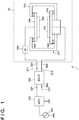
- Fig. 1 schematically shows the arrangement of a plasma processing apparatus 1 according to the first embodiment of the present invention.
- the plasma processing apparatus 1 includes a balun (balanced/unbalanced conversion circuit) 103, a vacuum container 110, a first electrode 106, and a second electrode 111.
- the plasma processing apparatus 1 includes the balun 103 and a main body 10
- the main body 10 includes the vacuum container 110, the first electrode 106, and the second electrode 111.
- the main body 10 includes a first terminal 251 and a second terminal 252.
- the balun 103 includes a first unbalanced terminal 201, a second unbalanced terminal 202, a first balanced terminal 211, and a second balanced terminal 212.
- An unbalanced circuit is connected to the first unbalanced terminal 201 and the second unbalanced terminal 202 of the balun 103, and a balanced circuit is connected to the first balanced terminal 211 and the second balanced terminal 212 of the balun 103.
- the vacuum container 110 is formed by a conductor, and is grounded.
- the first electrode 106 serves as a cathode, and holds a target 109.
- the target 109 can be, for example, an insulator material or a conductor material.
- the second electrode 111 serves as an anode, and holds a substrate 112.
- the plasma processing apparatus 1 according to the first embodiment can operate as a sputtering apparatus that forms a film on the substrate 112 by sputtering the target 109.
- the first electrode 106 is electrically connected to the first balanced terminal 211
- the second electrode 111 is electrically connected to the second balanced terminal 212.
- the above arrangement can be understood as an arrangement in which the first electrode 106 is electrically connected to the first terminal 251, the second electrode 111 is electrically connected to the second terminal 252, the first terminal 251 is electrically connected to the first balanced terminal 211, and the second terminal 252 is electrically connected to the second balanced terminal 212.
- the first electrode 106 and the first balanced terminal 211 are electrically connected via a blocking capacitor 104.
- the blocking capacitor 104 blocks a DC current between the first balanced terminal 211 and the first electrode 106 (or between the first balanced terminal 211 and the second balanced terminal 212).
- an impedance matching circuit 102 (to be described later) may be configured to block a DC current flowing between the first unbalanced terminal 201 and the second unbalanced terminal 202.
- the first electrode 106 can be supported by the vacuum container 110 via an insulator 107.
- the second electrode 111 can be supported by the vacuum container 110 via an insulator 108.
- the insulator 108 can be arranged between the second electrode 111 and the vacuum container 110.
- the plasma processing apparatus 1 can further include a high-frequency power supply 101, and the impedance matching circuit 102 arranged between the high-frequency power supply 101 and the balun 103.
- the high-frequency power supply 101 supplies a high frequency (high-frequency current, high-frequency voltage, and high-frequency power) between the first unbalanced terminal 201 and the second unbalanced terminal 202 of the balun 103 via the impedance matching circuit 102.
- the high-frequency power supply 101 supplies a high frequency (high-frequency current, high-frequency voltage, and high-frequency power) between the first electrode 106 and the second electrode 111 via the impedance matching circuit 102, the balun 103, and the blocking capacitor 104.
- the high-frequency power supply 101 can be understood to supply a high frequency between the first terminal 251 and the second terminal 252 of the main body 10 via the impedance matching circuit 102 and the balun 103.
- a gas for example, Ar, Kr, or Xe gas
- a gas supply unit (not shown) provided in the vacuum container 110.
- the high-frequency power supply 101 supplies a high frequency between the first electrode 106 and the second electrode 111 via the impedance matching circuit 102, the balun 103, and the blocking capacitor 104. This generates plasma between the first electrode 106 and the second electrode 111, and generates a self-bias voltage on the surface of the target 109 to cause ions in the plasma to collide against the surface of the target 109, thereby discharging, from the target 109, the particles of a material constituting the target 109. Then, the particles form a film on the substrate 112.
- Fig. 2A shows an example of the arrangement of the balun 103.
- the balun 103 shown in Fig. 2A includes a first coil 221 that connects the first unbalanced terminal 201 and the first balanced terminal 211, and a second coil 222 that connects the second unbalanced terminal 202 and the second balanced terminal 212.
- the first coil 221 and the second coil 222 are coils having the same number of turns, and share an iron core.
- Fig. 2B shows another example of the arrangement of the balun 103.
- the balun 103 shown in Fig. 2B includes a first coil 221 that connects the first unbalanced terminal 201 and the first balanced terminal 211, and a second coil 222 that connects the second unbalanced terminal 202 and the second balanced terminal 212.
- the first coil 221 and the second coil 222 are coils having the same number of turns, and share an iron core.
- the balun 103 shown in Fig. 2B further includes a third coil 223 and a fourth coil 224 both of which are connected between the first balanced terminal 211 and the second balanced terminal 212.
- the third coil 223 and the fourth coil 224 are configured so that the voltage of a connection node 213 of the third coil 223 and the fourth coil 224 is set as the midpoint between the voltage of the first balanced terminal 211 and that of the second balanced terminal 212.
- the third coil 223 and the fourth coil 224 are coils having the same number of turns, and share an iron core.
- the connection node 213 may be grounded, may be connected to the vacuum container 110, or may be floated.
- balun 103 The function of the balun 103 will be described with reference to Fig. 3 .
- I1 be a current flowing through the first unbalanced terminal 201
- 12 be a current flowing through the first balanced terminal 211
- 12' be a current flowing through the second unbalanced terminal 202
- 13 be a current, of the current 12, flowing to ground.
- 13 0, that is, no current flows to ground on the balanced circuit side
- the isolation performance of the balanced circuit with respect to ground is lowest.
- Rp - jXp represents an impedance (including the reactance of the blocking capacitor 104) when viewing the side of the first electrode 106 and the second electrode 111 (the side of the main body 10) from the side of the first balanced terminal 211 and the second balanced terminal 212 in a state in which plasma is generated in the internal space of the vacuum container 110.
- Rp represents a resistance component
- -Xp represents a reactance component.
- X represents the reactance component (inductance component) of the impedance of the first coil 221 of the balun 103.
- ISO has a correlation with X/Rp.
- the present inventor found that when 1.5 ⁇ X/Rp ⁇ 5000 is satisfied, the potential (plasma potential) of plasma formed in the internal space (the space between the first electrode 106 and the second electrode 111) of the vacuum container 110 is insensitive to the state of the inner surface of the vacuum container 110. When the plasma potential is insensitive to the state of the inner surface of the vacuum container 110, this indicates that it is possible to stabilize the plasma potential even if the plasma processing apparatus 1 is used for a long period.
- 1.5 ⁇ X/Rp ⁇ 5000 corresponds to -10.0 dB ⁇ ISO ⁇ -80 dB.
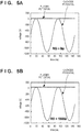
- Figs. 5A to 5D each show a result of simulating the plasma potential and the potential (cathode potential) of the first electrode 106 when 1.5 ⁇ X/Rp ⁇ 5000 is satisfied.
- Fig. 5A shows the plasma potential and the cathode potential in a state in which no film is formed on the inner surface of the vacuum container 110.
- Fig. 5B shows the plasma potential and the cathode potential in a state in which a resistive film (1,000 ⁇ ) is formed on the inner surface of the vacuum container 110.
- Fig. 5C shows the plasma potential and the cathode potential in a state in which an inductive film (0.6 ⁇ H) is formed on the inner surface of the vacuum container 110.
- Fig. 5A shows the plasma potential and the cathode potential in a state in which no film is formed on the inner surface of the vacuum container 110.
- Fig. 5B shows the plasma potential and the cathode potential in a state in which a resistive film (1,000 ⁇
- FIG. 5D shows the plasma potential and the cathode potential in a state in which a capacitive film (0.1 nF) is formed on the inner surface of the vacuum container 110.
- a capacitive film 0.1 nF
- Figs. 6A to 6D each show a result of simulating the plasma potential and the potential (cathode potential) of the first electrode 106 when 1.5 ⁇ X/Rp ⁇ 5000 is not satisfied.
- Fig. 6A shows the plasma potential and the cathode potential in a state in which no film is formed on the inner surface of the vacuum container 110.
- Fig. 6B shows the plasma potential and the cathode potential in a state in which a resistive film (1,000 ⁇ ) is formed on the inner surface of the vacuum container 110.
- Fig. 6C shows the plasma potential and the cathode potential in a state in which an inductive film (0.6 ⁇ H) is formed on the inner surface of the vacuum container 110.
- Fig. 6A shows the plasma potential and the cathode potential in a state in which no film is formed on the inner surface of the vacuum container 110.
- Fig. 6B shows the plasma potential and the cathode potential in a state in which a resistive film (1,000
- FIG. 6D shows the plasma potential and the cathode potential in a state in which a capacitive film (0.1 nF) is formed on the inner surface of the vacuum container 110.
- the plasma potential readily changes depending on the state of the inner surface of the vacuum container 110. If X/Rp > 5000 is satisfied, in a state in which no film is formed on the inner surface of the vacuum container 110, discharge occurs only between the first electrode 106 and the second electrode 111. However, if X/Rp > 5000 is satisfied, when a film starts to be formed on the inner surface of the vacuum container 110, the plasma potential sensitively reacts to this, and the results exemplified in Figs.
- the plasma processing apparatus 1 should be configured to satisfy 1.5 ⁇ X/Rp ⁇ 5000.
- a method of deciding Rp - jXp (it is desired to actually know only Rp) will be exemplified with reference to Fig. 7 .
- the balun 103 is detached from the plasma processing apparatus 1 and an output terminal 230 of the impedance matching circuit 102 is connected to the first terminal 251 (blocking capacitor 104) of the main body 10. Furthermore, the second terminal 252 (second electrode 111) of the main body 10 is grounded.
- the high-frequency power supply 101 supplies a high frequency to the first terminal 251 of the main body 10 via the impedance matching circuit 102.
- the impedance matching circuit 102 is equivalently formed by coils L1 and L2 and variable capacitors VC1 and VC2.
- the impedance of the impedance matching circuit 102 matches the impedance Rp - jXp on the side of the main body 10 (the side of the first electrode 106 and the second electrode 111) when the plasma is generated.
- the impedance of the impedance matching circuit 102 at this time is given by Rp + jXp.
- Rp - jXp (it is desired to actually know only Rp) can be obtained based on the impedance Rp + jXp of the impedance matching circuit 102 when the impedance is matched.
- Rp - jXp can be obtained by simulation based on design data.
- the reactance component (inductance component) X of the impedance of the first coil 221 of the balun 103 is decided so as to satisfy 1.5 ⁇ X/Rp ⁇ 5000.
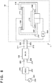
- Fig. 8 schematically shows the arrangement of a plasma processing apparatus 1 according to the second embodiment of the present invention.
- the plasma processing apparatus 1 according to the second embodiment can operate as an etching apparatus that etches a substrate 112.
- a first electrode 106 serves as a cathode, and holds the substrate 112.
- a second electrode 111 serves as an anode.
- the first electrode 106 and a first balanced terminal 211 are electrically connected via a blocking capacitor 104.
- the blocking capacitor 104 is arranged in an electrical connection path between the first electrode 106 and the first balanced terminal 211.
- Fig. 9 schematically shows the arrangement of a plasma processing apparatus 1 according to the third embodiment of the present invention.
- the plasma processing apparatus 1 according to the third embodiment is a modification of the plasma processing apparatus 1 according to the first embodiment, and further includes at least one of a mechanism for vertically moving a second electrode 111 and a mechanism for rotating the second electrode 111.
- the plasma processing apparatus 1 includes a driving mechanism 114 having both the mechanism for vertically moving the second electrode 111 and the mechanism for rotating the second electrode 111.
- a bellows 113 forming a vacuum partition can be provided between a vacuum container 110 and the driving mechanism 114.
- the plasma processing apparatus 1 can further include at least one of a mechanism for vertically moving the first electrode 106 and a mechanism for rotating the first electrode 106.
- Fig. 10 schematically shows the arrangement of a plasma processing apparatus 1 according to the fourth embodiment of the present invention. Items which are not referred to as the plasma processing apparatus 1 according to the fourth embodiment can comply with the first to third embodiments.
- the plasma processing apparatus 1 includes a first balun 103, a second balun 303, a vacuum container 110, a first electrode 106, and a second electrode 135 constituting the first pair, and a first electrode 141 and a second electrode 145 constituting the second pair.
- the plasma processing apparatus 1 includes the first balun 103, the second balun 303, and a main body 10, and the main body 10 includes the vacuum container 110, the first electrode 106 and the second electrode 135 constituting the first pair, and the first electrode 141 and the second electrode 145 constituting the second pair.
- the main body 10 includes a first terminal 251, a second terminal 252, a third terminal 451, and a fourth terminal 452.
- the first balun 103 includes a first unbalanced terminal 201, a second unbalanced terminal 202, a first balanced terminal 211, and a second balanced terminal 212.
- An unbalanced circuit is connected to the first unbalanced terminal 201 and the second unbalanced terminal 202 of the first balun 103, and a balanced circuit is connected to the first balanced terminal 211 and the second balanced terminal 212 of the first balun 103.
- the second balun 303 can have an arrangement similar to that of the first balun 103.
- the second balun 303 includes a first unbalanced terminal 401, a second unbalanced terminal 402, a first balanced terminal 411, and a second balanced terminal 412.
- An unbalanced circuit is connected to the first unbalanced terminal 401 and the second unbalanced terminal 402 of the second balun 303, and a balanced circuit is connected to the first balanced terminal 411 and the second balanced terminal 412 of the second balun 303.
- the vacuum container 110 is grounded.
- the first electrode 106 of the first pair holds a target 109.
- the target 109 can be, for example, an insulator material or a conductor material.
- the second electrode 135 of the first pair is arranged around the first electrode 106.
- the first electrode 106 of the first pair is electrically connected to the first balanced terminal 211 of the first balun 103, and the second electrode 135 of the first pair is electrically connected to the second balanced terminal 212 of the first balun 103.
- the first electrode 141 of the second pair holds a substrate 112.
- the second electrode 145 of the second pair is arranged around the first electrode 141.
- the first electrode 141 of the second pair is electrically connected to the first balanced terminal 411 of the second balun 303, and the second electrode 145 of the second pair is electrically connected to the second balanced terminal 412 of the second balun 303.
- the above arrangement can be understood as an arrangement in which the first electrode 106 of the first pair is electrically connected to the first terminal 251, the second electrode 135 of the first pair is electrically connected to the second terminal 252, the first terminal 251 is electrically connected to the first balanced terminal 211 of the first balun 103, and the second terminal 252 is electrically connected to the second balanced terminal 212 of the first balun 103.
- the above arrangement can be understood as an arrangement in which the first electrode 141 of the second pair is electrically connected to the third terminal 451, the second electrode 145 of the second pair is electrically connected to the fourth terminal 452, the third terminal 451 is electrically connected to the first balanced terminal 411 of the second balun 303, and the fourth terminal 452 is electrically connected to the second balanced terminal 412 of the second balun 303.
- the first electrode 106 of the first pair and the first balanced terminal 211 (first terminal 251) of the first balun 103 can electrically be connected via a blocking capacitor 104.
- the blocking capacitor 104 blocks a DC current between the first balanced terminal 211 of the first balun 103 and the first electrode 106 of the first pair (or between the first balanced terminal 211 and the second balanced terminal 212 of the first balun 103).
- a first impedance matching circuit 102 may be configured to block a DC current flowing between the first unbalanced terminal 201 and the second unbalanced terminal 202 of the first balun 103.
- the first electrode 106 and the second electrode 135 of the first pair can be supported by the vacuum container 110 via an insulator 132.
- the first electrode 141 of the second pair and the first balanced terminal 411 (third terminal 451) of the second balun 303 can electrically be connected via a blocking capacitor 304.
- the blocking capacitor 304 blocks a DC current between the first balanced terminal 411 of the second balun 303 and the first electrode 141 of the second pair (or between the first balanced terminal 411 and the second balanced terminal 412 of the second balun 303).
- a second impedance matching circuit 302 may be configured to block a DC current flowing between the first unbalanced terminal 201 and the second unbalanced terminal 202 of the second balun 303.
- the first electrode 141 and the second electrode 145 of the second pair can be supported by the vacuum container 110 via an insulator 142.
- the plasma processing apparatus 1 can include a first high-frequency power supply 101, and the first impedance matching circuit 102 arranged between the first high-frequency power supply 101 and the first balun 103.
- the first high-frequency power supply 101 supplies a high frequency between the first unbalanced terminal 201 and the second unbalanced terminal 202 of the first balun 103 via the first impedance matching circuit 102.
- the first high-frequency power supply 101 supplies a high frequency between the first electrode 106 and the second electrode 135 via the first impedance matching circuit 102, the first balun 103, and the blocking capacitor 104.
- the first high-frequency power supply 101 supplies a high frequency between the first terminal 251 and the second terminal 252 of the main body 10 via the first impedance matching circuit 102 and the first balun 103.
- the first balun 103 and the first electrode 106 and the second electrode 135 of the first pair form the first high-frequency supply unit that supplies a high frequency to the internal space of the vacuum container 110.
- the plasma processing apparatus 1 can include a second high-frequency power supply 301, and the second impedance matching circuit 302 arranged between the second high-frequency power supply 301 and the second balun 303.
- the second high-frequency power supply 301 supplies a high frequency between the first unbalanced terminal 401 and the second unbalanced terminal 402 of the second balun 303 via the second impedance matching circuit 302.
- the second high-frequency power supply 301 supplies a high frequency between the first electrode 141 and the second electrode 145 of the second pair via the second impedance matching circuit 302, the second balun 303, and the blocking capacitor 304.
- the second high-frequency power supply 301 supplies a high frequency between the third terminal 451 and the fourth terminal 452 of the main body 10 via the second impedance matching circuit 302 and the second balun 303.
- the second balun 303 and the first electrode 141 and the second electrode 145 of the second pair form the second high-frequency supply unit that supplies a high frequency to the internal space of the vacuum container 110.
- Rp1 - jXp1 be an impedance when viewing the side of the first electrode 106 and the second electrode 135 of the first pair (the side of the main body 10) from the side of the first balanced terminal 211 and the second balanced terminal 212 of the first balun 103 in a state in which plasma is generated in the internal space of the vacuum container 110 by supplying a high frequency from the first high-frequency power supply 101.
- X1 be the reactance component (inductance component) of the impedance of a first coil 221 of the first balun 103. In this definition, when 1.5 ⁇ X1/Rp1 ⁇ 5000 is satisfied, the potential of the plasma formed in the internal space of the vacuum container 110 can be stabilized.
- Rp2 - jXp2 be an impedance when viewing the side of the first electrode 141 and the second electrode 145 of the second pair (the side of the main body 10) from the side of the first balanced terminal 411 and the second balanced terminal 412 of the second balun 303 in a state in which plasma is generated in the internal space of the vacuum container 110 by supplying a high frequency from the second high-frequency power supply 301.
- X2 be the reactance component (inductance component) of the impedance of a first coil 221 of the second balun 303. In this definition, when 1.5 ⁇ X2/Rp2 ⁇ 5000 is satisfied, the potential of the plasma formed in the internal space of the vacuum container 110 can be stabilized.
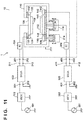
- Fig. 11 schematically shows the arrangement of a plasma processing apparatus 1 according to the fifth embodiment of the present invention.
- the apparatus 1 according to the fifth embodiment has an arrangement obtained by adding driving mechanisms 114 and 314 to the plasma processing apparatus 1 according to the fourth embodiment.
- the driving mechanism 114 can include at least one of a mechanism for vertically moving a first electrode 141 and a mechanism for rotating the first electrode 141.
- the driving mechanism 314 can include a mechanism for vertically moving a second electrode 145.
- Fig. 12 schematically shows the arrangement of a plasma processing apparatus 1 according to the sixth embodiment of the present invention. Items which are not referred to as the sixth embodiment can comply with the first to fifth embodiments.
- the plasma processing apparatus 1 according to the sixth embodiment includes a plurality of first high-frequency supply units and at least one second high-frequency supply unit.
- One of the plurality of first high-frequency supply units can include a first electrode 106a, a second electrode 135a, and a first balun 103a.
- Another one of the plurality of first high-frequency supply units can include a first electrode 106b, a second electrode 135b, and a first balun 103b.
- An example in which the plurality of first high-frequency supply units are formed by two high-frequency supply units will be described.
- the two high-frequency supply units and constituent elements associated with them are distinguished from each other using subscripts a and b.
- two targets are distinguished from each other using subscripts a and b.
- the plasma processing apparatus 1 includes the plurality of first baluns 103a and 103b, a second balun 303, a vacuum container 110, the first electrode 106a and the second electrode 135a, the first electrode 106b and the second electrode 135b, and a first electrode 141 and a second electrode 145.
- the plasma processing apparatus 1 includes the plurality of first baluns 103a and 103b, the second balun 303, and a main body 10
- the main body 10 includes the vacuum container 110, the first electrode 106a and the second electrode 135a, the first electrode 106b and the second electrode 135b, and the first electrode 141 and the second electrode 145.
- the main body 10 includes first terminals 251a and 251b, second terminals 252a and 252b, a third terminal 451, and a fourth terminal 452.
- the first balun 103a includes a first unbalanced terminal 201a, a second unbalanced terminal 202a, a first balanced terminal 211a, and a second balanced terminal 212a.
- An unbalanced circuit is connected to the first unbalanced terminal 201a and the second unbalanced terminal 202a of the first balun 103a, and a balanced circuit is connected to the first balanced terminal 211a and the second balanced terminal 212a of the first balun 103a.
- the first balun 103b includes a first unbalanced terminal 201b, a second unbalanced terminal 202b, a first balanced terminal 211b, and a second balanced terminal 212b.
- An unbalanced circuit is connected to the first unbalanced terminal 201b and the second unbalanced terminal 202b of the first balun 103b, and a balanced circuit is connected to the first balanced terminal 211b and the second balanced terminal 212b of the first balun 103b.
- the second balun 303 can have an arrangement similar to that of the first balun 103a or 103b.
- the second balun 303 includes a first unbalanced terminal 401, a second unbalanced terminal 402, a first balanced terminal 411, and a second balanced terminal 412.
- An unbalanced circuit is connected to the first unbalanced terminal 401 and the second unbalanced terminal 402 of the second balun 303, and a balanced circuit is connected to the first balanced terminal 411 and the second balanced terminal 412 of the second balun 303.
- the vacuum container 110 is grounded.
- the first electrodes 106a and 106b hold targets 109a and 109b, respectively.
- Each of the targets 109a and 109b can be, for example, an insulator material or a conductor material.
- the second electrodes 135a and 135b are arranged around the first electrodes 106a and 106b, respectively.
- the first electrodes 106a and 106b are electrically connected to the first balanced terminals 211a and 211b of the first baluns 103a and 103b, respectively, and the second electrodes 135a and 135b are electrically connected to the second balanced terminals 212a and 212b of the first baluns 103a and 103b, respectively.
- the first electrode 141 holds a substrate 112.
- the second electrode 145 is arranged around the first electrode 141.
- the first electrode 141 is electrically connected to the first balanced terminal 411 of the second balun 303, and the second electrode 145 is electrically connected to the second balanced terminal 412 of the second balun 303.
- the above arrangement can be understood as an arrangement in which the first electrodes 106a and 106b are electrically connected to the first terminals 251a and 251b, respectively, the second electrodes 135a and 135b are electrically connected to the second terminals 252a and 252b, respectively, the first terminals 251a and 251b are electrically connected to the first balanced terminals 211a and 111b of the first baluns 103a and 103b, respectively, and the second terminals 252a and 252b are electrically be connected to the second balanced terminals 212a and 212b of the first baluns 103a and 103b, respectively.
- the above arrangement can be understood as an arrangement in which the first electrode 141 is electrically connected to the third terminal 451, the second electrode 145 is electrically connected to the fourth terminal 452, the third terminal 451 is electrically connected to the first balanced terminal 411 of the second balun 303, and the fourth terminal 452 is electrically connected to the second balanced terminal 412 of the second balun 303.
- the first electrodes 106a and 106b and the first balanced terminals 211a and 211b (first terminals 251a and 251b) of the first baluns 103a and 103b can electrically be connected via blocking capacitors 104a and 104b, respectively.
- the blocking capacitors 104a and 104b block DC currents between the first electrodes 106a and 106b and the first balanced terminals 211a and 211b of the first baluns 103a and 103b (or between the first balanced terminals 211a and 211b and the second balanced terminals 212a and 212b of the first baluns 103a and 103b), respectively.
- first impedance matching circuits 102a and 102b may be configured to block DC currents flowing between the first unbalanced terminals 201a and 201b and the second unbalanced terminals 202a and 202b of the first baluns 103a and 103b, respectively.
- the blocking capacitors 104a and 104b may be arranged between the second electrodes 135a and 135b and the second balanced terminals 212a and 212b (second terminals 252a and 252b) of the first baluns 103a and 103b, respectively.
- the first electrodes 106a and 106b and the second electrodes 135a and 135b can be supported by the vacuum container 110 via insulators 132a and 132b, respectively.
- the first electrode 141 and the first balanced terminal 411 (third terminal 451) of the second balun 303 can electrically be connected via a blocking capacitor 304.
- the blocking capacitor 304 blocks a DC current between the first electrode 141 and the first balanced terminal 411 of the second balun 303 (or between the first balanced terminal 411 and the second balanced terminal 412 of the second balun 303).
- a second impedance matching circuit 302 may be configured to block a DC current flowing between the first unbalanced terminal 201 and the second unbalanced terminal 202 of the second balun 303.
- the blocking capacitor 304 may be arranged between the second electrode 145 and the second balanced terminal 412 (fourth terminal 452) of the second balun 303.
- the first electrode 141 and the second electrode 145 can be supported by the vacuum container 110 via an insulator 142.
- the plasma processing apparatus 1 can include a plurality of first high-frequency power supplies 101a and 101b, and the first impedance matching circuits 102a and 102b respectively arranged between the plurality of first high-frequency power supplies 101a and 101b and the plurality of first baluns 103a and 103b.
- the first high-frequency power supplies 101a and 101b supply high frequencies between the first unbalanced terminals 201a and 201b and the second unbalanced terminals 202a and 202b of the first baluns 103a and 103b via the first impedance matching circuits 102a and 102b, respectively.
- the first high-frequency power supplies 101a and 101b supply high frequencies between the first electrodes 106a and 106b and the second electrodes 135a and 135b via the first impedance matching circuits 102a and 102b, the first baluns 103a and 103b, and the blocking capacitors 104a and 104b, respectively.
- the first high-frequency power supplies 101a and 101b supply high frequencies between the first terminals 251a and 251b and the second terminals 252a and 252b of the main body 10 via the first impedance matching circuits 102a and 102b and the first baluns 103a and 103b.
- the plasma processing apparatus 1 can include a second high-frequency power supply 301, and the second impedance matching circuit 302 arranged between the second high-frequency power supply 301 and the second balun 303.
- the second high-frequency power supply 301 supplies a high frequency between the first unbalanced terminal 401 and the second unbalanced terminal 402 of the second balun 303 via the second impedance matching circuit 302.
- the second high-frequency power supply 301 supplies a high frequency between the first electrode 141 and the second electrode 145 via the second impedance matching circuit 302, the second balun 303, and the blocking capacitor 304.
- the second high-frequency power supply 301 supplies a high frequency between the third terminal 451 and the fourth terminal 452 of the main body 10 via the second impedance matching circuit 302 and the second balun 303.
- Fig. 13 schematically shows the arrangement of a plasma processing apparatus 1 according to the seventh embodiment of the present invention. Items which are not referred to as the sputtering apparatus 1 according to the seventh embodiment can comply with the first to sixth embodiments.
- the plasma processing apparatus 1 includes a first balun 103, a second balun 303, a vacuum container 110, a first electrode 105a and a second electrode 105b constituting the first pair, and a first electrode 141 and a second electrode 145 constituting the second pair.
- the plasma processing apparatus 1 includes the first balun 103, the second balun 303, and a main body 10, and the main body 10 includes the vacuum container 110, the first electrode 105a and the second electrode 105b constituting the first pair, and the first electrode 141 and the second electrode 145 constituting the second pair.
- the main body 10 includes a first terminal 251, a second terminal 252, a third terminal 451 and a fourth terminal 452.
- the first balun 103 includes a first unbalanced terminal 201, a second unbalanced terminal 202, a first balanced terminal 211, and a second balanced terminal 212.
- An unbalanced circuit is connected to the first unbalanced terminal 201 and the second unbalanced terminal 202 of the first balun 103, and a balanced circuit is connected to the first balanced terminal 211 and the second balanced terminal 212 of the first balun 103.
- the second balun 303 can have an arrangement similar to that of the first balun 103.
- the second balun 303 includes a first unbalanced terminal 401, a second unbalanced terminal 402, a first balanced terminal 411, and a second balanced terminal 412.
- An unbalanced circuit is connected to the first unbalanced terminal 401 and the second unbalanced terminal 402 of the second balun 303, and a balanced circuit is connected to the first balanced terminal 411 and the second balanced terminal 412 of the second balun 303.
- the vacuum container 110 is grounded.
- the first electrode 105a of the first pair holds a first target 109a, and opposes a space on the side of a substrate 112 via the first target 109a.
- the second electrode 105b of the first pair is arranged adjacent to the first electrode 105a, holds a second target 109b, and opposes the space on the side of the substrate 112 via the second target 109b.
- Each of the targets 109a and 109b can be, for example, an insulator material or a conductor material.
- the first electrode 105a of the first pair is electrically connected to the first balanced terminal 211 of the first balun 103, and the second electrode 105b of the first pair is electrically connected to the second balanced terminal 212 of the first balun 103.
- the first electrode 141 of the second pair holds the substrate 112.
- the second electrode 145 of the second pair is arranged around the first electrode 141.
- the first electrode 141 of the second pair is electrically connected to the first balanced terminal 411 of the second balun 303, and the second electrode 145 of the second pair is electrically connected to the second balanced terminal 412 of the second balun 303.
- the above arrangement can be understood as an arrangement in which the first electrode 105a of the first pair is electrically connected to the first terminal 251, the second electrode 105b of the first pair is electrically connected to the second terminal 252, the first terminal 251 is electrically connected to the first balanced terminal 211 of the first balun 103, and the second terminal 252 is connected to the second balanced terminal 212 of the first balun 103.
- the above arrangement can be understood as an arrangement in which the first electrode 141 of the second pair is electrically connected to the third terminal 451, the second electrode 145 of the second pair is electrically connected to the fourth terminal 452, the third terminal 451 is electrically connected to the first balanced terminal 411 of the second balun 303, and the fourth terminal 452 is connected to the second balanced terminal 412 of the second balun 303.
- the first electrode 105a of the first pair and the first balanced terminal 211 (first terminal 251) of the first balun 103 can electrically be connected via a blocking capacitor 104a.
- the blocking capacitor 104a blocks a DC current between the first balanced terminal 211 of the first balun 103 and the first electrode 105a of the first pair (or between the first balanced terminal 211 and the second balanced terminal 212 of the first balun 103).
- the second electrode 105b of the first pair and the second balanced terminal 212 (second terminal 252) of the first balun 103 can electrically be connected via a blocking capacitor 104b.
- the blocking capacitor 104b blocks a DC current between the second balanced terminal 212 of the first balun 103 and the second electrode 105b of the first pair (or between the first balanced terminal 211 and the second balanced terminal 212 of the first balun 103).
- the first electrode 105a and the second electrode 105b of the first pair can be supported by the vacuum container 110 via insulators 132a and 132b, respectively.
- the first electrode 141 of the second pair and the first balanced terminal 411 (third terminal 451) of the second balun 303 can electrically be connected via a blocking capacitor 304.
- the blocking capacitor 304 blocks a DC current between the first balanced terminal 411 of the second balun 303 and the first electrode 141 of the second pair (or between the first balanced terminal 411 and the second balanced terminal 412 of the second balun 303).
- a second impedance matching circuit 302 may be configured to block a DC current flowing between the first unbalanced terminal 401 and the second unbalanced terminal 402 of the second balun 303.
- the first electrode 141 and the second electrode 145 of the second pair can be supported by the vacuum container 110 via insulators 142 and 146, respectively.
- the plasma processing apparatus 1 can include a first high-frequency power supply 101, and a first impedance matching circuit 102 arranged between the first high-frequency power supply 101 and the first balun 103.
- the first high-frequency power supply 101 supplies a high frequency between the first electrode 105a and the second electrode 105b via the first impedance matching circuit 102, the first balun 103, and the blocking capacitors 104a and 104b.
- the first high-frequency power supply 101 supplies a high frequency between the first terminal 251 and the second terminal 252 of the main body 10 via the first impedance matching circuit 102 and the first balun 103.
- the first balun 103 and the first electrode 105a and the second electrode 105b of the first pair form the first high-frequency supply unit that supplies a high frequency to the internal space of the vacuum container 110.
- the plasma processing apparatus 1 can include a second high-frequency power supply 301, and the second impedance matching circuit 302 arranged between the second high-frequency power supply 301 and the second balun 303.
- the second high-frequency power supply 301 supplies a high frequency between the first unbalanced terminal 401 and the second unbalanced terminal 402 of the second balun 303 via the second impedance matching circuit 302.
- the second high-frequency power supply 301 supplies a high frequency between the first electrode 141 and the second electrode 145 of the second pair via the second impedance matching circuit 302, the second balun 303, and the blocking capacitor 304.
- the second high-frequency power supply 301 supplies a high frequency between the third terminal 451 and the fourth terminal 452 of the main body 10 via the second impedance matching circuit 302 and the second balun 303.
- the second balun 303 and the first electrode 141 and the second electrode 145 of the second pair form the second high-frequency supply unit that supplies a high frequency to the internal space of the vacuum container 110.
- Rp1 - jXp1 be an impedance when viewing the side of the first electrode 105a and the second electrode 105b of the first pair (the side of the main body 10) from the side of the first balanced terminal 211 and the second balanced terminal 212 of the first balun 103 in a state in which plasma is generated in the internal space of the vacuum container 110 by supplying a high frequency from the first high-frequency power supply 101.
- X1 be the reactance component (inductance component) of the impedance of a first coil 221 of the first balun 103. In this definition, when 1.5 ⁇ X1/Rp1 ⁇ 5000 is satisfied, the potential of the plasma formed in the internal space of the vacuum container 110 can be stabilized.
- Rp2 - jXp2 be an impedance when viewing the side of a first electrode 127 and a second electrode 130 of the second pair (the side of the main body 10) from the side of the first balanced terminal 411 and the second balanced terminal 412 of the second balun 303 in a state in which plasma is generated in the internal space of the vacuum container 110 by supplying a high frequency from the second high-frequency power supply 302.
- Let X2 be the reactance component (inductance component) of the impedance of a first coil 221 of the second balun 303. In this definition, when 1.5 ⁇ X2/Rp2 ⁇ 5000 is satisfied, the potential of the plasma formed in the internal space of the vacuum container 110 can be stabilized.
- the sputtering apparatus 1 according to the seventh embodiment can further include at least one of a mechanism for vertically moving the first electrode 141 constituting the second pair and a mechanism for rotating the first electrode 141 constituting the second pair.
- the plasma processing apparatus 1 includes a driving mechanism 114 having both the mechanism for vertically moving the first electrode 141 and the mechanism for rotating the first electrode 141.
- the plasma processing apparatus 1 includes a driving mechanism 314 for vertically moving the second electrode constituting the second pair. Bellows forming vacuum partitions can be provided between a vacuum container 113 and the driving mechanisms 114 and 314.
- Rp represents a resistance component
- -Xp represents a reactance component.
- X represents the reactance component (inductance component) of the impedance of the first coil 221 of the balun 103.
- ISO has a correlation with X/Rp.
- the relationship shown in Fig. 4 also holds in the seventh embodiment.
- the present inventor found that in the seventh embodiment as well, when 1.5 ⁇ X/Rp ⁇ 5000 is satisfied, the potential (plasma potential) of plasma formed in the internal space (the space between the first electrode 105a and the second electrode 105b) of the vacuum container 110 is insensitive to the state of the inner surface of the vacuum container 110.
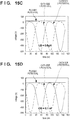
- Figs. 15A to 15D each show the plasma potential, the potential (cathode 1 potential) of the first electrode 105a, and the potential (cathode 2 potential) of the second electrode 105b when 1.5 ⁇ X/Rp ⁇ 5000 is satisfied.
- Fig. 15A shows the plasma potential, the potential (cathode 1 potential) of the first electrode 105a, and the potential (cathode 2 potential) of the second electrode 105b in a state in which a resistive film (1 m ⁇ ) is formed on the inner surface of the vacuum container 110.
- Fig. 15A shows the plasma potential, the potential (cathode 1 potential) of the first electrode 105a, and the potential (cathode 2 potential) of the second electrode 105b in a state in which a resistive film (1 m ⁇ ) is formed on the inner surface of the vacuum container 110.
- FIG. 15B shows the plasma potential, the potential (cathode 1 potential) of the first electrode 105a, and the potential (cathode 2 potential) of the second electrode 105b in a state in which a resistive film (1,000 ⁇ ) is formed on the inner surface of the vacuum container 110.
- Fig. 15C shows the plasma potential, the potential (cathode 1 potential) of the first electrode 105a, and the potential (cathode 2 potential) of the second electrode 105b in a state in which an inductive film (0.6 ⁇ H) is formed on the inner surface of the vacuum container 110.
- FIG. 15D shows the plasma potential, the potential (cathode 1 potential) of the first electrode 105a, and the potential (cathode 2 potential) of the second electrode 105b in a state in which a capacitive film (0.1 nF) is formed on the inner surface of the vacuum container 110.
- a capacitive film 0.1 nF
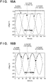
- Figs. 16A to 16D each show a result of simulating the plasma potential, the potential (cathode 1 potential) of the first electrode 105a, and the potential (cathode 2 potential) of the second electrode 105b when 1.5 ⁇ X/Rp ⁇ 5000 is not satisfied.
- Fig. 16A shows the plasma potential, the potential (cathode 1 potential) of the first electrode 105a, and the potential (cathode 2 potential) of the second electrode 105b in a state in which a resistive film (1 m ⁇ ) is formed on the inner surface of the vacuum container 110.
- FIG. 16B shows the plasma potential, the potential (cathode 1 potential) of the first electrode 105a, and the potential (cathode 2 potential) of the second electrode 105b in a state in which a resistive film (1,000 ⁇ ) is formed on the inner surface of the vacuum container 110.
- Fig. 16C shows the plasma potential, the potential (cathode 1 potential) of the first electrode 105a, and the potential (cathode 2 potential) of the second electrode 105b in a state in which an inductive film (0.6 ⁇ H) is formed on the inner surface of the vacuum container 110.
- FIG. 16D shows the plasma potential, the potential (cathode 1 potential) of the first electrode 105a, and the potential (cathode 2 potential) of the second electrode 105b in a state in which a capacitive film (0.1 nF) is formed on the inner surface of the vacuum container 110.
- a capacitive film 0.1 nF
- the plasma potential readily changes depending on the state of the inner surface of the vacuum container 110. If X/Rp > 5000 is satisfied, in a state in which no film is formed on the inner surface of the vacuum container 110, discharge occurs only between the first electrode 105a and the second electrode 105b. However, if X/Rp > 5000 is satisfied, when a film starts to be formed on the inner surface of the vacuum container 110, the plasma potential sensitively reacts to this, and the results exemplified in Figs.
- the sputtering apparatus 1 should be configured to satisfy 1.5 ⁇ X/Rp ⁇ 5000.
Landscapes
- Chemical & Material Sciences (AREA)
- Engineering & Computer Science (AREA)
- Physics & Mathematics (AREA)
- Plasma & Fusion (AREA)
- Analytical Chemistry (AREA)
- Mechanical Engineering (AREA)
- Chemical Kinetics & Catalysis (AREA)
- Materials Engineering (AREA)
- Metallurgy (AREA)
- Organic Chemistry (AREA)
- General Chemical & Material Sciences (AREA)
- Electromagnetism (AREA)
- Spectroscopy & Molecular Physics (AREA)
- Plasma Technology (AREA)
- Drying Of Semiconductors (AREA)
- Physical Vapour Deposition (AREA)
Priority Applications (1)
| Application Number | Priority Date | Filing Date | Title |
|---|---|---|---|
| PL17915645T PL3648550T3 (pl) | 2017-06-27 | 2017-06-27 | Urządzenie do przetwarzania plazmowego |
Applications Claiming Priority (1)
| Application Number | Priority Date | Filing Date | Title |
|---|---|---|---|
| PCT/JP2017/023611 WO2019003312A1 (ja) | 2017-06-27 | 2017-06-27 | プラズマ処理装置 |
Publications (3)
| Publication Number | Publication Date |
|---|---|
| EP3648550A1 true EP3648550A1 (de) | 2020-05-06 |
| EP3648550A4 EP3648550A4 (de) | 2020-06-24 |
| EP3648550B1 EP3648550B1 (de) | 2021-06-02 |
Family
ID=61195801
Family Applications (1)
| Application Number | Title | Priority Date | Filing Date |
|---|---|---|---|
| EP17915645.0A Active EP3648550B1 (de) | 2017-06-27 | 2017-06-27 | Plasmabehandlungsvorrichtung |
Country Status (9)
| Country | Link |
|---|---|
| US (1) | US11626270B2 (de) |
| EP (1) | EP3648550B1 (de) |
| JP (1) | JP6280677B1 (de) |
| KR (2) | KR102457976B1 (de) |
| CN (1) | CN110800375B (de) |
| PL (1) | PL3648550T3 (de) |
| SG (1) | SG11201912566WA (de) |
| TW (2) | TWI704844B (de) |
| WO (1) | WO2019003312A1 (de) |
Cited By (1)
| Publication number | Priority date | Publication date | Assignee | Title |
|---|---|---|---|---|
| WO2022066839A3 (en) * | 2020-09-23 | 2022-06-16 | Advanced Energy Industries, Inc. | Alternating current (ac) dual magnetron sputtering |
Families Citing this family (9)
| Publication number | Priority date | Publication date | Assignee | Title |
|---|---|---|---|---|
| JP6516951B1 (ja) * | 2017-06-27 | 2019-05-22 | キヤノンアネルバ株式会社 | プラズマ処理装置 |
| PL3648554T3 (pl) * | 2017-06-27 | 2021-11-22 | Canon Anelva Corporation | Urządzenie do przetwarzania plazmowego |
| CN114666965B (zh) * | 2017-06-27 | 2025-08-01 | 佳能安内华股份有限公司 | 等离子体处理装置 |
| EP4017223B1 (de) | 2017-06-27 | 2025-10-15 | Canon Anelva Corporation | Plasmaverarbeitungsvorrichtung |
| JP6656479B2 (ja) * | 2017-06-27 | 2020-03-04 | キヤノンアネルバ株式会社 | プラズマ処理装置および方法 |
| EP3648550B1 (de) * | 2017-06-27 | 2021-06-02 | Canon Anelva Corporation | Plasmabehandlungsvorrichtung |
| TWI690244B (zh) * | 2017-06-27 | 2020-04-01 | 日商佳能安內華股份有限公司 | 電漿處理裝置 |
| PL3817517T3 (pl) * | 2018-06-26 | 2024-10-28 | Canon Anelva Corporation | Urządzenie do obróbki plazmą, sposób obróbki plazmą, program oraz nośnik pamięci |
| KR102799065B1 (ko) | 2021-05-18 | 2025-04-23 | 캐논 아네르바 가부시키가이샤 | 적층체 및 적층체의 제조 방법 |
Family Cites Families (172)
| Publication number | Priority date | Publication date | Assignee | Title |
|---|---|---|---|---|
| US4025339A (en) | 1974-01-18 | 1977-05-24 | Coulter Information Systems, Inc. | Electrophotographic film, method of making the same and photoconductive coating used therewith |
| US4014779A (en) | 1974-11-01 | 1977-03-29 | Coulter Information Systems, Inc. | Sputtering apparatus |
| JPS53141937U (de) | 1977-04-15 | 1978-11-09 | ||
| US4170475A (en) | 1977-05-12 | 1979-10-09 | Coulter Information Systems, Inc. | High speed electrophotographic method |
| JPS53141937A (en) | 1977-05-18 | 1978-12-11 | Mitsubishi Electric Corp | Liquid fuel burner |
| US4131533A (en) | 1977-12-30 | 1978-12-26 | International Business Machines Corporation | RF sputtering apparatus having floating anode shield |
| JPS5535465A (en) | 1978-09-05 | 1980-03-12 | Hitachi Cable | Method of coloring insulated wire |
| US4284490A (en) | 1978-09-28 | 1981-08-18 | Coulter Systems Corporation | R.F. Sputtering apparatus including multi-network power supply |
| US4284489A (en) | 1978-09-28 | 1981-08-18 | Coulter Systems Corporation | Power transfer network |
| JPS57106216A (en) | 1980-12-24 | 1982-07-02 | Fujitsu Ltd | Switched capacitor filter |
| US4584079A (en) | 1983-10-11 | 1986-04-22 | Honeywell Inc. | Step shape tailoring by phase angle variation RF bias sputtering |
| JPH0639693B2 (ja) | 1985-12-05 | 1994-05-25 | 日電アネルバ株式会社 | 誘電体バイアススパツタリング装置 |
| US4887005A (en) * | 1987-09-15 | 1989-12-12 | Rough J Kirkwood H | Multiple electrode plasma reactor power distribution system |
| US5121067A (en) * | 1987-10-06 | 1992-06-09 | Board Of Regents Of Leland Stanford University | Directional sampling bridge |
| US4802080A (en) | 1988-03-18 | 1989-01-31 | American Telephone And Telegraph Company, At&T Information Systems | Power transfer circuit including a sympathetic resonator |
| US4956582A (en) * | 1988-04-19 | 1990-09-11 | The Boeing Company | Low temperature plasma generator with minimal RF emissions |
| US4871421A (en) * | 1988-09-15 | 1989-10-03 | Lam Research Corporation | Split-phase driver for plasma etch system |
| JPH02156083A (ja) * | 1988-12-09 | 1990-06-15 | Tokuda Seisakusho Ltd | スパッタ装置 |
| JPH02156082A (ja) | 1988-12-09 | 1990-06-15 | Tokuda Seisakusho Ltd | スパッタ装置 |
| JPH02156080A (ja) * | 1988-12-09 | 1990-06-15 | Tokuda Seisakusho Ltd | スパッタ装置 |
| JPH02156081A (ja) * | 1988-12-09 | 1990-06-15 | Tokuda Seisakusho Ltd | スパッタ装置 |
| JP3016821B2 (ja) * | 1990-06-15 | 2000-03-06 | 東京エレクトロン株式会社 | プラズマ処理方法 |
| US5316645A (en) * | 1990-08-07 | 1994-05-31 | Canon Kabushiki Kaisha | Plasma processing apparatus |
| DE4106770C2 (de) | 1991-03-04 | 1996-10-17 | Leybold Ag | Verrichtung zum reaktiven Beschichten eines Substrats |
| US5330578A (en) | 1991-03-12 | 1994-07-19 | Semiconductor Energy Laboratory Co., Ltd. | Plasma treatment apparatus |
| JPH04317325A (ja) | 1991-04-17 | 1992-11-09 | Nec Corp | 半導体装置の製造装置 |
| US5415757A (en) | 1991-11-26 | 1995-05-16 | Leybold Aktiengesellschaft | Apparatus for coating a substrate with electrically nonconductive coatings |
| US5286297A (en) * | 1992-06-24 | 1994-02-15 | Texas Instruments Incorporated | Multi-electrode plasma processing apparatus |
| US5698082A (en) | 1993-08-04 | 1997-12-16 | Balzers Und Leybold | Method and apparatus for coating substrates in a vacuum chamber, with a system for the detection and suppression of undesirable arcing |
| JP2642849B2 (ja) | 1993-08-24 | 1997-08-20 | 株式会社フロンテック | 薄膜の製造方法および製造装置 |
| AU2003195A (en) * | 1994-06-21 | 1996-01-04 | Boc Group, Inc., The | Improved power distribution for multiple electrode plasma systems using quarter wavelength transmission lines |
| US5830331A (en) | 1994-09-23 | 1998-11-03 | Seagate Technology, Inc. | Apparatus and method for sputtering carbon |
| DE19537212A1 (de) | 1994-10-06 | 1996-04-11 | Leybold Ag | Vorrichtung zum Beschichten von Substraten im Vakuum |
| US5989999A (en) * | 1994-11-14 | 1999-11-23 | Applied Materials, Inc. | Construction of a tantalum nitride film on a semiconductor wafer |
| DE4441206C2 (de) | 1994-11-19 | 1996-09-26 | Leybold Ag | Einrichtung für die Unterdrückung von Überschlägen in Kathoden-Zerstäubungseinrichtungen |
| EP0831679B1 (de) | 1995-06-05 | 2008-10-01 | Musashino Kikai Co., Ltd. | Leistungsversorgung für multielektroden-entladung |
| DE19540543A1 (de) | 1995-10-31 | 1997-05-07 | Leybold Ag | Vorrichtung zum Beschichten eines Substrats mit Hilfe des Chemical-Vapor-Deposition-Verfahrens |
| DE19540794A1 (de) | 1995-11-02 | 1997-05-07 | Leybold Ag | Vorrichtung zum Beschichten eines Substrats von einem elektrisch leitfähigen Target |
| US5830272A (en) | 1995-11-07 | 1998-11-03 | Sputtered Films, Inc. | System for and method of providing a controlled deposition on wafers |
| US6017221A (en) * | 1995-12-04 | 2000-01-25 | Flamm; Daniel L. | Process depending on plasma discharges sustained by inductive coupling |
| US6252354B1 (en) * | 1996-11-04 | 2001-06-26 | Applied Materials, Inc. | RF tuning method for an RF plasma reactor using frequency servoing and power, voltage, current or DI/DT control |
| DE19651811B4 (de) | 1996-12-13 | 2006-08-31 | Unaxis Deutschland Holding Gmbh | Vorrichtung zum Belegen eines Substrats mit dünnen Schichten |
| KR100252210B1 (ko) | 1996-12-24 | 2000-04-15 | 윤종용 | 반도체장치 제조용 건식식각장치 |
| JP3598717B2 (ja) | 1997-03-19 | 2004-12-08 | 株式会社日立製作所 | プラズマ処理装置 |
| DE19713637C2 (de) | 1997-04-02 | 1999-02-18 | Max Planck Gesellschaft | Teilchenmanipulierung |
| GB9714142D0 (en) | 1997-07-05 | 1997-09-10 | Surface Tech Sys Ltd | An arrangement for the feeding of RF power to one or more antennae |
| JP3356043B2 (ja) | 1997-12-26 | 2002-12-09 | 三菱電機株式会社 | レーザ加工装置用距離検出器 |
| US6273022B1 (en) * | 1998-03-14 | 2001-08-14 | Applied Materials, Inc. | Distributed inductively-coupled plasma source |
| JP3148177B2 (ja) * | 1998-04-27 | 2001-03-19 | ニチメン電子工研株式会社 | プラズマ処理装置 |
| JP2000030896A (ja) | 1998-07-10 | 2000-01-28 | Anelva Corp | プラズマ閉込め装置 |
| US6046641A (en) * | 1998-07-22 | 2000-04-04 | Eni Technologies, Inc. | Parallel HV MOSFET high power stable amplifier |
| JP3166745B2 (ja) | 1998-12-25 | 2001-05-14 | 日本電気株式会社 | プラズマ処理装置ならびにプラズマ処理方法 |
| US20020022836A1 (en) * | 1999-03-05 | 2002-02-21 | Gyrus Medical Limited | Electrosurgery system |
| JP2000294543A (ja) | 1999-04-08 | 2000-10-20 | Hitachi Ltd | エッチング方法およびエッチング装置ならびに半導体装置の製造方法 |
| KR100748798B1 (ko) | 1999-05-06 | 2007-08-13 | 동경 엘렉트론 주식회사 | 플라즈마 에칭 장치 |
| US6818103B1 (en) | 1999-10-15 | 2004-11-16 | Advanced Energy Industries, Inc. | Method and apparatus for substrate biasing in multiple electrode sputtering systems |
| JP2003512526A (ja) | 1999-10-15 | 2003-04-02 | アドバンスト・エナジー・インダストリーズ・インコーポレイテッド | 複数の電極のスパッタリングシステムにおいて基板にバイアスをかける方法および装置 |
| JP2001122690A (ja) * | 1999-10-26 | 2001-05-08 | Toyo Kohan Co Ltd | マイクロ波プラズマcvd装置及びダイヤモンド薄膜を形成する方法 |
| MXPA02004936A (es) | 1999-11-16 | 2003-06-30 | Centre D'innovation Sur Le Transport D'energie Du Quebec | Metodo y aparato para facilitar el reencendido en un horno de arco. |
| JP4601104B2 (ja) | 1999-12-20 | 2010-12-22 | キヤノンアネルバ株式会社 | プラズマ処理装置 |
| WO2001088966A2 (en) | 2000-05-12 | 2001-11-22 | Tokyo Electron Limited | Method of adjusting the thickness of an electrode in a plasma processing system |
| JP4656697B2 (ja) | 2000-06-16 | 2011-03-23 | キヤノンアネルバ株式会社 | 高周波スパッタリング装置 |
| US7294563B2 (en) * | 2000-08-10 | 2007-11-13 | Applied Materials, Inc. | Semiconductor on insulator vertical transistor fabrication and doping process |
| JP3911555B2 (ja) | 2000-08-15 | 2007-05-09 | 独立行政法人産業技術総合研究所 | シリコン系薄膜の製造法 |
| JP3807598B2 (ja) | 2001-07-23 | 2006-08-09 | 東京エレクトロン株式会社 | エッチング方法 |
| DE10154229B4 (de) | 2001-11-07 | 2004-08-05 | Applied Films Gmbh & Co. Kg | Einrichtung für die Regelung einer Plasmaimpedanz |
| JP2003155556A (ja) | 2001-11-16 | 2003-05-30 | Canon Inc | ウエッジ形状膜の製造法 |
| WO2003055286A1 (en) | 2001-12-10 | 2003-07-03 | Tokyo Electron Limited | High-frequency power source and its control method, and plasma processor |
| US7298091B2 (en) * | 2002-02-01 | 2007-11-20 | The Regents Of The University Of California | Matching network for RF plasma source |
| US6703080B2 (en) | 2002-05-20 | 2004-03-09 | Eni Technology, Inc. | Method and apparatus for VHF plasma processing with load mismatch reliability and stability |
| DE10326135B4 (de) | 2002-06-12 | 2014-12-24 | Ulvac, Inc. | Entladungsplasma-Bearbeitungsanlage |
| US7445690B2 (en) | 2002-10-07 | 2008-11-04 | Tokyo Electron Limited | Plasma processing apparatus |
| US7032536B2 (en) | 2002-10-11 | 2006-04-25 | Sharp Kabushiki Kaisha | Thin film formation apparatus including engagement members for support during thermal expansion |
| US7309998B2 (en) * | 2002-12-02 | 2007-12-18 | Burns Lawrence M | Process monitor for monitoring an integrated circuit chip |
| DE10306347A1 (de) | 2003-02-15 | 2004-08-26 | Hüttinger Elektronik GmbH & Co. KG | Leistungszufuhrregeleinheit |
| US6876205B2 (en) | 2003-06-06 | 2005-04-05 | Advanced Energy Industries, Inc. | Stored energy arc detection and arc reduction circuit |
| US6972079B2 (en) | 2003-06-25 | 2005-12-06 | Advanced Energy Industries Inc. | Dual magnetron sputtering apparatus utilizing control means for delivering balanced power |
| JP3575011B1 (ja) * | 2003-07-04 | 2004-10-06 | 村田 正義 | プラズマ表面処理装置およびプラズマ表面処理方法 |
| JP2005130376A (ja) | 2003-10-27 | 2005-05-19 | Sony Corp | バラン |
| US7126346B2 (en) | 2003-12-18 | 2006-10-24 | Agilent Technologies, Inc. | Method, apparatus, and article of manufacture for manufacturing high frequency balanced circuits |
| US7241361B2 (en) | 2004-02-20 | 2007-07-10 | Fei Company | Magnetically enhanced, inductively coupled plasma source for a focused ion beam system |
| JP4658506B2 (ja) | 2004-03-31 | 2011-03-23 | 浩史 滝川 | パルスアークプラズマ生成用電源回路及びパルスアークプラズマ処理装置 |
| JP2005303257A (ja) | 2004-10-01 | 2005-10-27 | Masayoshi Murata | 高周波プラズマ生成用平衡不平衡変換装置と、該平衡不平衡変換装置により構成されたプラズマ表面処理装置およびプラズマ表面処理方法 |
| JP4909523B2 (ja) | 2005-03-30 | 2012-04-04 | 株式会社ユーテック | スパッタリング装置及びスパッタリング方法 |
| EP1720195B1 (de) | 2005-05-06 | 2012-12-12 | HÜTTINGER Elektronik GmbH + Co. KG | Arcunterdrückungsanordnung |
| JP2006336084A (ja) | 2005-06-03 | 2006-12-14 | Canon Inc | スパッタ成膜方法 |
| CN2907173Y (zh) | 2006-02-24 | 2007-05-30 | 苏州大学 | 大面积并联高密度感应耦合等离子体源 |
| US7517437B2 (en) | 2006-03-29 | 2009-04-14 | Applied Materials, Inc. | RF powered target for increasing deposition uniformity in sputtering systems |
| US8932430B2 (en) | 2011-05-06 | 2015-01-13 | Axcelis Technologies, Inc. | RF coupled plasma abatement system comprising an integrated power oscillator |
| EP2087778A4 (de) * | 2006-08-22 | 2010-11-17 | Mattson Tech Inc | Induktive plasmaquelle mit hohem koppelwirkungsgrad |
| US10083817B1 (en) * | 2006-08-22 | 2018-09-25 | Valery Godyak | Linear remote plasma source |
| JP4768699B2 (ja) * | 2006-11-30 | 2011-09-07 | キヤノンアネルバ株式会社 | 電力導入装置及び成膜方法 |
| US7777567B2 (en) | 2007-01-25 | 2010-08-17 | Mks Instruments, Inc. | RF power amplifier stability network |
| US20170213734A9 (en) * | 2007-03-30 | 2017-07-27 | Alexei Marakhtanov | Multifrequency capacitively coupled plasma etch chamber |
| US8450635B2 (en) | 2007-03-30 | 2013-05-28 | Lam Research Corporation | Method and apparatus for inducing DC voltage on wafer-facing electrode |
| JP2008300322A (ja) | 2007-06-04 | 2008-12-11 | Canon Anelva Corp | プラズマ処理装置、プラズマ処理方法、整合器、及び整合器の動作方法 |
| US20090075597A1 (en) | 2007-09-18 | 2009-03-19 | Ofir Degani | Device, system, and method of low-noise amplifier |
| TWI440405B (zh) | 2007-10-22 | 2014-06-01 | New Power Plasma Co Ltd | 電容式耦合電漿反應器 |
| JP2009135448A (ja) | 2007-11-01 | 2009-06-18 | Semiconductor Energy Lab Co Ltd | 半導体基板の作製方法及び半導体装置の作製方法 |
| PT2211916E (pt) | 2007-11-06 | 2016-01-11 | Creo Medical Ltd | Sistema de esterilização por plasma de micro-ondas e respetivos aplicadores |
| JP5371238B2 (ja) | 2007-12-20 | 2013-12-18 | 東京エレクトロン株式会社 | プラズマ処理装置およびプラズマ処理方法 |
| CN101478857A (zh) * | 2008-01-04 | 2009-07-08 | 北京北方微电子基地设备工艺研究中心有限责任公司 | 等离子体处理装置 |
| JP5294669B2 (ja) * | 2008-03-25 | 2013-09-18 | 東京エレクトロン株式会社 | プラズマ処理装置 |
| JP2008294465A (ja) * | 2008-07-31 | 2008-12-04 | Masayoshi Murata | 電流導入端子と、該電流導入端子を備えたプラズマ表面処理装置及びプラズマ表面処理方法 |
| JP2010045664A (ja) | 2008-08-14 | 2010-02-25 | Tokyo Electron Ltd | マッチング装置、マッチング方法、プラズマ処理装置、及び記憶媒体 |
| JP2008300873A (ja) | 2008-08-26 | 2008-12-11 | Masayoshi Murata | プラズマ表面処理方法及びプラズマ表面処理装置 |
| US8438990B2 (en) | 2008-09-30 | 2013-05-14 | Applied Materials, Inc. | Multi-electrode PECVD source |
| JP4547711B2 (ja) * | 2008-10-10 | 2010-09-22 | 村田 正義 | 高周波プラズマcvd装置及び高周波プラズマcvd法 |
| JP5305287B2 (ja) | 2008-10-30 | 2013-10-02 | 芝浦メカトロニクス株式会社 | 半導体製造装置 |
| US20110300694A1 (en) | 2008-11-12 | 2011-12-08 | Ulvac, Inc. | Electrode circuit, film formation device, electrode unit, and film formation method |
| WO2010094002A2 (en) | 2009-02-13 | 2010-08-19 | Applied Materials, Inc. | Rf bus and rf return bus for plasma chamber electrode |
| JP2010255061A (ja) * | 2009-04-27 | 2010-11-11 | Canon Anelva Corp | スパッタリング装置及びスパッタリング処理方法 |
| JP2009302566A (ja) * | 2009-09-16 | 2009-12-24 | Masayoshi Murata | トランス型平衡不平衡変換装置を備えたプラズマ表面処理装置 |
| US9039864B2 (en) | 2009-09-29 | 2015-05-26 | Applied Materials, Inc. | Off-center ground return for RF-powered showerhead |
| US8755204B2 (en) * | 2009-10-21 | 2014-06-17 | Lam Research Corporation | RF isolation for power circuitry |
| US8501631B2 (en) * | 2009-11-19 | 2013-08-06 | Lam Research Corporation | Plasma processing system control based on RF voltage |
| EP2326151A1 (de) * | 2009-11-24 | 2011-05-25 | AGC Glass Europe | Verfahren und Vorrichtung zur Polarisierung einer DBD-Elektrode |
| JP2011144450A (ja) | 2009-12-16 | 2011-07-28 | Canon Anelva Corp | スパッタリング装置及びスパッタリング方法 |
| JP5606063B2 (ja) | 2009-12-28 | 2014-10-15 | 東京エレクトロン株式会社 | プラズマ処理装置 |
| DE102010031568B4 (de) | 2010-07-20 | 2014-12-11 | TRUMPF Hüttinger GmbH + Co. KG | Arclöschanordnung und Verfahren zum Löschen von Arcs |
| CN102479657A (zh) | 2010-11-26 | 2012-05-30 | 沈阳拓荆科技有限公司 | 一种多段式匹配器 |
| JP5642531B2 (ja) | 2010-12-22 | 2014-12-17 | 東京エレクトロン株式会社 | 基板処理装置及び基板処理方法 |
| JP2012142332A (ja) | 2010-12-28 | 2012-07-26 | Canon Anelva Corp | 電子部品の製造方法 |
| KR20130099151A (ko) | 2011-01-12 | 2013-09-05 | 니신 일렉트릭 컴패니 리미티드 | 플라스마 장치 |
| KR101839776B1 (ko) | 2011-02-18 | 2018-03-20 | 삼성디스플레이 주식회사 | 플라즈마 처리장치 |
| CN106024568B (zh) | 2011-03-30 | 2019-05-21 | 周星工程股份有限公司 | 等离子体发生装置及基板处理装置 |
| US20130017315A1 (en) | 2011-07-15 | 2013-01-17 | Applied Materials, Inc. | Methods and apparatus for controlling power distribution in substrate processing systems |
| JP2013098177A (ja) * | 2011-10-31 | 2013-05-20 | Semes Co Ltd | 基板処理装置及びインピーダンスマッチング方法 |
| CN103091042B (zh) * | 2011-11-07 | 2016-11-16 | 泰州市宏华冶金机械有限公司 | 重心测量装置及重心测量方法 |
| CN104024471B (zh) * | 2011-12-27 | 2016-03-16 | 佳能安内华股份有限公司 | 溅射装置 |
| US9171699B2 (en) * | 2012-02-22 | 2015-10-27 | Lam Research Corporation | Impedance-based adjustment of power and frequency |
| US10157729B2 (en) * | 2012-02-22 | 2018-12-18 | Lam Research Corporation | Soft pulsing |
| US10325759B2 (en) | 2012-02-22 | 2019-06-18 | Lam Research Corporation | Multiple control modes |
| US9197196B2 (en) * | 2012-02-22 | 2015-11-24 | Lam Research Corporation | State-based adjustment of power and frequency |
| WO2013136656A1 (ja) | 2012-03-15 | 2013-09-19 | 東京エレクトロン株式会社 | 成膜装置 |
| DE102012103938A1 (de) * | 2012-05-04 | 2013-11-07 | Reinhausen Plasma Gmbh | Plasmamodul für eine Plasmaerzeugungsvorrichtung und Plasmaerzeugungsvorrichtung |
| US20130337657A1 (en) * | 2012-06-19 | 2013-12-19 | Plasmasi, Inc. | Apparatus and method for forming thin protective and optical layers on substrates |
| CN104488065B (zh) | 2012-07-24 | 2017-09-05 | Ev 集团 E·索尔纳有限责任公司 | 永久结合晶圆的方法及装置 |
| JP2014049541A (ja) * | 2012-08-30 | 2014-03-17 | Mitsubishi Heavy Ind Ltd | 薄膜製造装置及びその電極電圧調整方法 |
| JP2014049667A (ja) * | 2012-09-03 | 2014-03-17 | Tokyo Electron Ltd | プラズマ処理装置及びこれを備えた基板処理装置 |
| US9779196B2 (en) * | 2013-01-31 | 2017-10-03 | Lam Research Corporation | Segmenting a model within a plasma system |
| US9620337B2 (en) * | 2013-01-31 | 2017-04-11 | Lam Research Corporation | Determining a malfunctioning device in a plasma system |
| KR102168064B1 (ko) * | 2013-02-20 | 2020-10-20 | 도쿄엘렉트론가부시키가이샤 | 플라즈마 처리 장치 및 플라즈마 처리 방법 |
| WO2014141601A1 (ja) | 2013-03-14 | 2014-09-18 | キヤノンアネルバ株式会社 | 成膜方法、半導体発光素子の製造方法、半導体発光素子、照明装置 |
| JP2013139642A (ja) * | 2013-04-02 | 2013-07-18 | Canon Anelva Corp | スパッタ成膜応用のためのプラズマ処理装置 |
| JP6574547B2 (ja) | 2013-12-12 | 2019-09-11 | 東京エレクトロン株式会社 | プラズマ処理装置及びプラズマ処理方法 |
| WO2015097942A1 (ja) | 2013-12-25 | 2015-07-02 | キヤノンアネルバ株式会社 | 基板加工方法及び半導体装置の製造方法 |
| US10081869B2 (en) * | 2014-06-10 | 2018-09-25 | Lam Research Corporation | Defect control in RF plasma substrate processing systems using DC bias voltage during movement of substrates |
| US10410889B2 (en) | 2014-07-25 | 2019-09-10 | Applied Materials, Inc. | Systems and methods for electrical and magnetic uniformity and skew tuning in plasma processing reactors |
| RU2735240C2 (ru) * | 2015-01-16 | 2020-10-29 | Антонио Франко СЕЛЬМО | Устройство, предназначенное по существу для резонирования, подходящее для передачи радиочастотной мощности, а также система, включающая в себя такое устройство и используемая для генерации плазмы |
| GB201502453D0 (en) | 2015-02-13 | 2015-04-01 | Spts Technologies Ltd | Plasma producing apparatus |
| US10049862B2 (en) * | 2015-04-17 | 2018-08-14 | Lam Research Corporation | Chamber with vertical support stem for symmetric conductance and RF delivery |
| JP6652635B2 (ja) | 2015-05-12 | 2020-02-26 | ラガーディア アンド アソシエイツ エルエルシー | 原子炉容器の分割のためのシステムおよび方法 |
| JP6539113B2 (ja) | 2015-05-28 | 2019-07-03 | 株式会社日立ハイテクノロジーズ | プラズマ処理装置およびプラズマ処理方法 |
| US9960009B2 (en) | 2015-07-17 | 2018-05-01 | Lam Research Corporation | Methods and systems for determining a fault in a gas heater channel |
| JP6678886B2 (ja) | 2016-05-26 | 2020-04-15 | 株式会社サムソン | 給水予熱装置の製造方法 |
| US10403476B2 (en) | 2016-11-09 | 2019-09-03 | Lam Research Corporation | Active showerhead |
| JP2018129224A (ja) * | 2017-02-09 | 2018-08-16 | 東京エレクトロン株式会社 | プラズマ処理装置 |
| US10544505B2 (en) | 2017-03-24 | 2020-01-28 | Applied Materials, Inc. | Deposition or treatment of diamond-like carbon in a plasma reactor |
| GB2562110A (en) * | 2017-05-05 | 2018-11-07 | Creo Medical Ltd | Apparatus for sterilising an instrument channel of a surgical scoping device |
| EP4017223B1 (de) | 2017-06-27 | 2025-10-15 | Canon Anelva Corporation | Plasmaverarbeitungsvorrichtung |
| PL3648554T3 (pl) * | 2017-06-27 | 2021-11-22 | Canon Anelva Corporation | Urządzenie do przetwarzania plazmowego |
| EP3648550B1 (de) * | 2017-06-27 | 2021-06-02 | Canon Anelva Corporation | Plasmabehandlungsvorrichtung |
| JP6516951B1 (ja) | 2017-06-27 | 2019-05-22 | キヤノンアネルバ株式会社 | プラズマ処理装置 |
| TWI677907B (zh) * | 2017-06-27 | 2019-11-21 | 日商佳能安內華股份有限公司 | 電漿處理裝置 |
| CN114666965B (zh) * | 2017-06-27 | 2025-08-01 | 佳能安内华股份有限公司 | 等离子体处理装置 |
| JP6309683B1 (ja) | 2017-10-31 | 2018-04-11 | キヤノンアネルバ株式会社 | プラズマ処理装置 |
| KR102697703B1 (ko) | 2018-06-14 | 2024-08-23 | 엠케이에스 인스트루먼츠 인코포레이티드 | 원격 플라즈마 공급원을 위한 라디칼 출력 모니터 및 사용 방법 |
| PL3817517T3 (pl) * | 2018-06-26 | 2024-10-28 | Canon Anelva Corporation | Urządzenie do obróbki plazmą, sposób obróbki plazmą, program oraz nośnik pamięci |
| US10354838B1 (en) * | 2018-10-10 | 2019-07-16 | Lam Research Corporation | RF antenna producing a uniform near-field Poynting vector |
| US11013075B2 (en) * | 2018-12-20 | 2021-05-18 | Nxp Usa, Inc. | RF apparatus with arc prevention using non-linear devices |
| US11232931B2 (en) * | 2019-10-21 | 2022-01-25 | Mks Instruments, Inc. | Intermodulation distortion mitigation using electronic variable capacitor |
-
2017
- 2017-06-27 EP EP17915645.0A patent/EP3648550B1/de active Active
- 2017-06-27 KR KR1020207001366A patent/KR102457976B1/ko active Active
- 2017-06-27 JP JP2017555725A patent/JP6280677B1/ja active Active
- 2017-06-27 PL PL17915645T patent/PL3648550T3/pl unknown
- 2017-06-27 WO PCT/JP2017/023611 patent/WO2019003312A1/ja not_active Ceased
- 2017-06-27 CN CN201780092518.4A patent/CN110800375B/zh active Active
- 2017-06-27 SG SG11201912566WA patent/SG11201912566WA/en unknown
- 2017-06-27 KR KR1020227006321A patent/KR20220031132A/ko not_active Ceased
-
2018
- 2018-02-14 TW TW108116911A patent/TWI704844B/zh active
- 2018-02-14 TW TW107105433A patent/TWI704842B/zh active
-
2019
- 2019-12-19 US US16/720,262 patent/US11626270B2/en active Active
Cited By (1)
| Publication number | Priority date | Publication date | Assignee | Title |
|---|---|---|---|---|
| WO2022066839A3 (en) * | 2020-09-23 | 2022-06-16 | Advanced Energy Industries, Inc. | Alternating current (ac) dual magnetron sputtering |
Also Published As
| Publication number | Publication date |
|---|---|
| KR102457976B1 (ko) | 2022-10-25 |
| TWI704844B (zh) | 2020-09-11 |
| US20200126768A1 (en) | 2020-04-23 |
| TWI704842B (zh) | 2020-09-11 |
| CN110800375B (zh) | 2021-12-28 |
| TW201933950A (zh) | 2019-08-16 |
| PL3648550T3 (pl) | 2021-11-22 |
| TW201906500A (zh) | 2019-02-01 |
| US11626270B2 (en) | 2023-04-11 |
| KR20220031132A (ko) | 2022-03-11 |
| WO2019003312A1 (ja) | 2019-01-03 |
| EP3648550B1 (de) | 2021-06-02 |
| EP3648550A4 (de) | 2020-06-24 |
| JP6280677B1 (ja) | 2018-02-14 |
| JPWO2019003312A1 (ja) | 2019-07-04 |
| SG11201912566WA (en) | 2020-01-30 |
| KR20200018654A (ko) | 2020-02-19 |
| CN110800375A (zh) | 2020-02-14 |
Similar Documents
| Publication | Publication Date | Title |
|---|---|---|
| EP3648554B1 (de) | Plasmaverarbeitungsvorrichtung | |
| EP3648550B1 (de) | Plasmabehandlungsvorrichtung | |
| EP3648551B1 (de) | Plasmabehandlungsvorrichtung | |
| TWI678425B (zh) | 電漿處理裝置 | |
| JP2019133929A (ja) | プラズマ処理装置 |
Legal Events
| Date | Code | Title | Description |
|---|---|---|---|
| STAA | Information on the status of an ep patent application or granted ep patent |
Free format text: STATUS: THE INTERNATIONAL PUBLICATION HAS BEEN MADE |
|
| PUAI | Public reference made under article 153(3) epc to a published international application that has entered the european phase |
Free format text: ORIGINAL CODE: 0009012 |
|
| STAA | Information on the status of an ep patent application or granted ep patent |
Free format text: STATUS: REQUEST FOR EXAMINATION WAS MADE |
|
| 17P | Request for examination filed |
Effective date: 20191223 |
|
| AK | Designated contracting states |
Kind code of ref document: A1 Designated state(s): AL AT BE BG CH CY CZ DE DK EE ES FI FR GB GR HR HU IE IS IT LI LT LU LV MC MK MT NL NO PL PT RO RS SE SI SK SM TR |
|
| AX | Request for extension of the european patent |
Extension state: BA ME |
|
| A4 | Supplementary search report drawn up and despatched |
Effective date: 20200525 |
|
| RIC1 | Information provided on ipc code assigned before grant |
Ipc: H01J 37/34 20060101ALI20200518BHEP Ipc: H01J 37/32 20060101ALI20200518BHEP Ipc: C23C 16/505 20060101ALI20200518BHEP Ipc: H05H 1/46 20060101AFI20200518BHEP |
|
| DAV | Request for validation of the european patent (deleted) | ||
| DAX | Request for extension of the european patent (deleted) | ||
| GRAP | Despatch of communication of intention to grant a patent |
Free format text: ORIGINAL CODE: EPIDOSNIGR1 |
|
| STAA | Information on the status of an ep patent application or granted ep patent |
Free format text: STATUS: GRANT OF PATENT IS INTENDED |
|
| INTG | Intention to grant announced |
Effective date: 20201223 |
|
| GRAS | Grant fee paid |
Free format text: ORIGINAL CODE: EPIDOSNIGR3 |
|
| GRAA | (expected) grant |
Free format text: ORIGINAL CODE: 0009210 |
|
| STAA | Information on the status of an ep patent application or granted ep patent |
Free format text: STATUS: THE PATENT HAS BEEN GRANTED |
|
| REG | Reference to a national code |
Ref country code: CH Ref legal event code: EP |
|
| AK | Designated contracting states |
Kind code of ref document: B1 Designated state(s): AL AT BE BG CH CY CZ DE DK EE ES FI FR GB GR HR HU IE IS IT LI LT LU LV MC MK MT NL NO PL PT RO RS SE SI SK SM TR |
|
| REG | Reference to a national code |
Ref country code: GB Ref legal event code: FG4D |
|
| REG | Reference to a national code |
Ref country code: AT Ref legal event code: REF Ref document number: 1399692 Country of ref document: AT Kind code of ref document: T Effective date: 20210615 |
|
| REG | Reference to a national code |
Ref country code: IE Ref legal event code: FG4D |
|
| REG | Reference to a national code |
Ref country code: DE Ref legal event code: R096 Ref document number: 602017039888 Country of ref document: DE |
|
| REG | Reference to a national code |
Ref country code: NL Ref legal event code: FP |
|
| REG | Reference to a national code |
Ref country code: FI Ref legal event code: FGE |
|
| REG | Reference to a national code |
Ref country code: LT Ref legal event code: MG9D |
|
| PG25 | Lapsed in a contracting state [announced via postgrant information from national office to epo] |
Ref country code: LT Free format text: LAPSE BECAUSE OF FAILURE TO SUBMIT A TRANSLATION OF THE DESCRIPTION OR TO PAY THE FEE WITHIN THE PRESCRIBED TIME-LIMIT Effective date: 20210602 Ref country code: HR Free format text: LAPSE BECAUSE OF FAILURE TO SUBMIT A TRANSLATION OF THE DESCRIPTION OR TO PAY THE FEE WITHIN THE PRESCRIBED TIME-LIMIT Effective date: 20210602 Ref country code: BG Free format text: LAPSE BECAUSE OF FAILURE TO SUBMIT A TRANSLATION OF THE DESCRIPTION OR TO PAY THE FEE WITHIN THE PRESCRIBED TIME-LIMIT Effective date: 20210902 |
|
| REG | Reference to a national code |
Ref country code: AT Ref legal event code: MK05 Ref document number: 1399692 Country of ref document: AT Kind code of ref document: T Effective date: 20210602 |
|
| PG25 | Lapsed in a contracting state [announced via postgrant information from national office to epo] |
Ref country code: GR Free format text: LAPSE BECAUSE OF FAILURE TO SUBMIT A TRANSLATION OF THE DESCRIPTION OR TO PAY THE FEE WITHIN THE PRESCRIBED TIME-LIMIT Effective date: 20210903 Ref country code: NO Free format text: LAPSE BECAUSE OF FAILURE TO SUBMIT A TRANSLATION OF THE DESCRIPTION OR TO PAY THE FEE WITHIN THE PRESCRIBED TIME-LIMIT Effective date: 20210902 Ref country code: LV Free format text: LAPSE BECAUSE OF FAILURE TO SUBMIT A TRANSLATION OF THE DESCRIPTION OR TO PAY THE FEE WITHIN THE PRESCRIBED TIME-LIMIT Effective date: 20210602 Ref country code: RS Free format text: LAPSE BECAUSE OF FAILURE TO SUBMIT A TRANSLATION OF THE DESCRIPTION OR TO PAY THE FEE WITHIN THE PRESCRIBED TIME-LIMIT Effective date: 20210602 Ref country code: SE Free format text: LAPSE BECAUSE OF FAILURE TO SUBMIT A TRANSLATION OF THE DESCRIPTION OR TO PAY THE FEE WITHIN THE PRESCRIBED TIME-LIMIT Effective date: 20210602 |
|
| PG25 | Lapsed in a contracting state [announced via postgrant information from national office to epo] |
Ref country code: SK Free format text: LAPSE BECAUSE OF FAILURE TO SUBMIT A TRANSLATION OF THE DESCRIPTION OR TO PAY THE FEE WITHIN THE PRESCRIBED TIME-LIMIT Effective date: 20210602 Ref country code: SM Free format text: LAPSE BECAUSE OF FAILURE TO SUBMIT A TRANSLATION OF THE DESCRIPTION OR TO PAY THE FEE WITHIN THE PRESCRIBED TIME-LIMIT Effective date: 20210602 Ref country code: ES Free format text: LAPSE BECAUSE OF FAILURE TO SUBMIT A TRANSLATION OF THE DESCRIPTION OR TO PAY THE FEE WITHIN THE PRESCRIBED TIME-LIMIT Effective date: 20210602 Ref country code: EE Free format text: LAPSE BECAUSE OF FAILURE TO SUBMIT A TRANSLATION OF THE DESCRIPTION OR TO PAY THE FEE WITHIN THE PRESCRIBED TIME-LIMIT Effective date: 20210602 Ref country code: RO Free format text: LAPSE BECAUSE OF FAILURE TO SUBMIT A TRANSLATION OF THE DESCRIPTION OR TO PAY THE FEE WITHIN THE PRESCRIBED TIME-LIMIT Effective date: 20210602 Ref country code: PT Free format text: LAPSE BECAUSE OF FAILURE TO SUBMIT A TRANSLATION OF THE DESCRIPTION OR TO PAY THE FEE WITHIN THE PRESCRIBED TIME-LIMIT Effective date: 20211004 Ref country code: CZ Free format text: LAPSE BECAUSE OF FAILURE TO SUBMIT A TRANSLATION OF THE DESCRIPTION OR TO PAY THE FEE WITHIN THE PRESCRIBED TIME-LIMIT Effective date: 20210602 Ref country code: AT Free format text: LAPSE BECAUSE OF FAILURE TO SUBMIT A TRANSLATION OF THE DESCRIPTION OR TO PAY THE FEE WITHIN THE PRESCRIBED TIME-LIMIT Effective date: 20210602 |
|
| REG | Reference to a national code |
Ref country code: DE Ref legal event code: R097 Ref document number: 602017039888 Country of ref document: DE |
|
| REG | Reference to a national code |
Ref country code: BE Ref legal event code: MM Effective date: 20210630 |
|
| PG25 | Lapsed in a contracting state [announced via postgrant information from national office to epo] |
Ref country code: MC Free format text: LAPSE BECAUSE OF FAILURE TO SUBMIT A TRANSLATION OF THE DESCRIPTION OR TO PAY THE FEE WITHIN THE PRESCRIBED TIME-LIMIT Effective date: 20210602 Ref country code: LU Free format text: LAPSE BECAUSE OF NON-PAYMENT OF DUE FEES Effective date: 20210627 |
|
| PLBE | No opposition filed within time limit |
Free format text: ORIGINAL CODE: 0009261 |
|
| STAA | Information on the status of an ep patent application or granted ep patent |
Free format text: STATUS: NO OPPOSITION FILED WITHIN TIME LIMIT |
|
| PG25 | Lapsed in a contracting state [announced via postgrant information from national office to epo] |
Ref country code: IE Free format text: LAPSE BECAUSE OF NON-PAYMENT OF DUE FEES Effective date: 20210627 Ref country code: DK Free format text: LAPSE BECAUSE OF FAILURE TO SUBMIT A TRANSLATION OF THE DESCRIPTION OR TO PAY THE FEE WITHIN THE PRESCRIBED TIME-LIMIT Effective date: 20210602 |
|
| 26N | No opposition filed |
Effective date: 20220303 |
|
| PG25 | Lapsed in a contracting state [announced via postgrant information from national office to epo] |
Ref country code: AL Free format text: LAPSE BECAUSE OF FAILURE TO SUBMIT A TRANSLATION OF THE DESCRIPTION OR TO PAY THE FEE WITHIN THE PRESCRIBED TIME-LIMIT Effective date: 20210602 |
|
| PG25 | Lapsed in a contracting state [announced via postgrant information from national office to epo] |
Ref country code: IT Free format text: LAPSE BECAUSE OF FAILURE TO SUBMIT A TRANSLATION OF THE DESCRIPTION OR TO PAY THE FEE WITHIN THE PRESCRIBED TIME-LIMIT Effective date: 20210602 Ref country code: BE Free format text: LAPSE BECAUSE OF NON-PAYMENT OF DUE FEES Effective date: 20210630 |
|
| PG25 | Lapsed in a contracting state [announced via postgrant information from national office to epo] |
Ref country code: CY Free format text: LAPSE BECAUSE OF FAILURE TO SUBMIT A TRANSLATION OF THE DESCRIPTION OR TO PAY THE FEE WITHIN THE PRESCRIBED TIME-LIMIT Effective date: 20210602 |
|
| PG25 | Lapsed in a contracting state [announced via postgrant information from national office to epo] |
Ref country code: HU Free format text: LAPSE BECAUSE OF FAILURE TO SUBMIT A TRANSLATION OF THE DESCRIPTION OR TO PAY THE FEE WITHIN THE PRESCRIBED TIME-LIMIT; INVALID AB INITIO Effective date: 20170627 |
|
| PG25 | Lapsed in a contracting state [announced via postgrant information from national office to epo] |
Ref country code: MK Free format text: LAPSE BECAUSE OF FAILURE TO SUBMIT A TRANSLATION OF THE DESCRIPTION OR TO PAY THE FEE WITHIN THE PRESCRIBED TIME-LIMIT Effective date: 20210602 |
|
| PG25 | Lapsed in a contracting state [announced via postgrant information from national office to epo] |
Ref country code: TR Free format text: LAPSE BECAUSE OF FAILURE TO SUBMIT A TRANSLATION OF THE DESCRIPTION OR TO PAY THE FEE WITHIN THE PRESCRIBED TIME-LIMIT Effective date: 20210602 |
|
| PG25 | Lapsed in a contracting state [announced via postgrant information from national office to epo] |
Ref country code: MT Free format text: LAPSE BECAUSE OF FAILURE TO SUBMIT A TRANSLATION OF THE DESCRIPTION OR TO PAY THE FEE WITHIN THE PRESCRIBED TIME-LIMIT Effective date: 20210602 |
|
| PGFP | Annual fee paid to national office [announced via postgrant information from national office to epo] |
Ref country code: NL Payment date: 20250516 Year of fee payment: 9 |
|
| PGFP | Annual fee paid to national office [announced via postgrant information from national office to epo] |
Ref country code: FI Payment date: 20250620 Year of fee payment: 9 |
|
| PGFP | Annual fee paid to national office [announced via postgrant information from national office to epo] |
Ref country code: DE Payment date: 20250429 Year of fee payment: 9 Ref country code: PL Payment date: 20250502 Year of fee payment: 9 |
|
| PGFP | Annual fee paid to national office [announced via postgrant information from national office to epo] |
Ref country code: GB Payment date: 20250508 Year of fee payment: 9 |
|
| PGFP | Annual fee paid to national office [announced via postgrant information from national office to epo] |
Ref country code: FR Payment date: 20250508 Year of fee payment: 9 |
|
| PGFP | Annual fee paid to national office [announced via postgrant information from national office to epo] |
Ref country code: CH Payment date: 20250701 Year of fee payment: 9 |