EP3780073A1 - Elektrodenstruktur - Google Patents
Elektrodenstruktur Download PDFInfo
- Publication number
- EP3780073A1 EP3780073A1 EP19785253.6A EP19785253A EP3780073A1 EP 3780073 A1 EP3780073 A1 EP 3780073A1 EP 19785253 A EP19785253 A EP 19785253A EP 3780073 A1 EP3780073 A1 EP 3780073A1
- Authority
- EP
- European Patent Office
- Prior art keywords
- semiconductor device
- thickness
- electrode
- resin
- electrode structure
- Prior art date
- Legal status (The legal status is an assumption and is not a legal conclusion. Google has not performed a legal analysis and makes no representation as to the accuracy of the status listed.)
- Pending
Links
Images


Classifications
-
- G—PHYSICS
- G06—COMPUTING OR CALCULATING; COUNTING
- G06K—GRAPHICAL DATA READING; PRESENTATION OF DATA; RECORD CARRIERS; HANDLING RECORD CARRIERS
- G06K19/00—Record carriers for use with machines and with at least a part designed to carry digital markings
- G06K19/06—Record carriers for use with machines and with at least a part designed to carry digital markings characterised by the kind of the digital marking, e.g. shape, nature, code
- G06K19/067—Record carriers with conductive marks, printed circuits or semiconductor circuit elements, e.g. credit or identity cards also with resonating or responding marks without active components
- G06K19/07—Record carriers with conductive marks, printed circuits or semiconductor circuit elements, e.g. credit or identity cards also with resonating or responding marks without active components with integrated circuit chips
- G06K19/077—Constructional details, e.g. mounting of circuits in the carrier
-
- G—PHYSICS
- G01—MEASURING; TESTING
- G01N—INVESTIGATING OR ANALYSING MATERIALS BY DETERMINING THEIR CHEMICAL OR PHYSICAL PROPERTIES
- G01N27/00—Investigating or analysing materials by the use of electric, electrochemical, or magnetic means
- G01N27/26—Investigating or analysing materials by the use of electric, electrochemical, or magnetic means by investigating electrochemical variables; by using electrolysis or electrophoresis
- G01N27/28—Electrolytic cell components
- G01N27/283—Means for supporting or introducing electrochemical probes
-
- G—PHYSICS
- G01—MEASURING; TESTING
- G01N—INVESTIGATING OR ANALYSING MATERIALS BY DETERMINING THEIR CHEMICAL OR PHYSICAL PROPERTIES
- G01N27/00—Investigating or analysing materials by the use of electric, electrochemical, or magnetic means
- G01N27/26—Investigating or analysing materials by the use of electric, electrochemical, or magnetic means by investigating electrochemical variables; by using electrolysis or electrophoresis
- G01N27/28—Electrolytic cell components
- G01N27/30—Electrodes, e.g. test electrodes; Half-cells
- G01N27/333—Ion-selective electrodes or membranes
-
- G—PHYSICS
- G01—MEASURING; TESTING
- G01N—INVESTIGATING OR ANALYSING MATERIALS BY DETERMINING THEIR CHEMICAL OR PHYSICAL PROPERTIES
- G01N27/00—Investigating or analysing materials by the use of electric, electrochemical, or magnetic means
- G01N27/26—Investigating or analysing materials by the use of electric, electrochemical, or magnetic means by investigating electrochemical variables; by using electrolysis or electrophoresis
- G01N27/416—Systems
-
- G—PHYSICS
- G06—COMPUTING OR CALCULATING; COUNTING
- G06K—GRAPHICAL DATA READING; PRESENTATION OF DATA; RECORD CARRIERS; HANDLING RECORD CARRIERS
- G06K19/00—Record carriers for use with machines and with at least a part designed to carry digital markings
-
- G—PHYSICS
- G06—COMPUTING OR CALCULATING; COUNTING
- G06K—GRAPHICAL DATA READING; PRESENTATION OF DATA; RECORD CARRIERS; HANDLING RECORD CARRIERS
- G06K19/00—Record carriers for use with machines and with at least a part designed to carry digital markings
- G06K19/04—Record carriers for use with machines and with at least a part designed to carry digital markings characterised by the shape
- G06K19/041—Constructional details
- G06K19/042—Constructional details the record carrier having a form factor of a credit card and including a small sized disc, e.g. a CD or DVD
-
- H—ELECTRICITY
- H10—SEMICONDUCTOR DEVICES; ELECTRIC SOLID-STATE DEVICES NOT OTHERWISE PROVIDED FOR
- H10W—GENERIC PACKAGES, INTERCONNECTIONS, CONNECTORS OR OTHER CONSTRUCTIONAL DETAILS OF DEVICES COVERED BY CLASS H10
- H10W74/00—Encapsulations, e.g. protective coatings
-
- H—ELECTRICITY
- H10—SEMICONDUCTOR DEVICES; ELECTRIC SOLID-STATE DEVICES NOT OTHERWISE PROVIDED FOR
- H10W—GENERIC PACKAGES, INTERCONNECTIONS, CONNECTORS OR OTHER CONSTRUCTIONAL DETAILS OF DEVICES COVERED BY CLASS H10
- H10W74/00—Encapsulations, e.g. protective coatings
- H10W74/01—Manufacture or treatment
- H10W74/016—Manufacture or treatment using moulds
-
- H—ELECTRICITY
- H10—SEMICONDUCTOR DEVICES; ELECTRIC SOLID-STATE DEVICES NOT OTHERWISE PROVIDED FOR
- H10W—GENERIC PACKAGES, INTERCONNECTIONS, CONNECTORS OR OTHER CONSTRUCTIONAL DETAILS OF DEVICES COVERED BY CLASS H10
- H10W74/00—Encapsulations, e.g. protective coatings
- H10W74/10—Encapsulations, e.g. protective coatings characterised by their shape or disposition
- H10W74/111—Encapsulations, e.g. protective coatings characterised by their shape or disposition the semiconductor body being completely enclosed
Definitions
- the present invention relates to an electrode structure.
- an analyzer for clinical examination it is required to record information such as an individual identification code, a period of use, a state of use, and the like for a purpose of reducing medical mistakes and quickly responding to occurrence of mistakes.
- an electrode on which a semiconductor device such as a memory card for recording this information is mounted, has been proposed (see PTL 1).
- the semiconductor device As a technique for miniaturizing the electrode on which the semiconductor device is mounted, a method of insert-molding the semiconductor device during injection-molding has been proposed.
- the semiconductor device and an electrode housing are integrated without any gap, and the electrode is miniaturized while maintaining characteristics of the semiconductor device.
- the semiconductor device such as a memory card may be bent and destructed by a pressure of a molten resin.
- a method of preventing deformation by supporting a bending side with a jig or the like has been proposed (see PTL 2).
- An object of the invention is to provide an electrode structure capable of preventing destruction of a semiconductor device without increasing a development period and a development cost.
- An electrode structure is an electrode formed by resin molding a semiconductor device, and includes a first resin mold portion formed on a front surface of the semiconductor device and having a first thickness, a second resin mold portion formed on a back surface of the semiconductor device and having a second thickness greater than the first thickness, and an exposed portion formed in a part of the first resin mold portion corresponding to an end of the semiconductor device.
- An electrode structure is an electrode formed by resin molding a semiconductor device, and includes a first resin mold portion formed on a front surface of the semiconductor device and having a first thickness, a second resin mold portion formed on a back surface of the semiconductor device and having a second thickness greater than the first thickness, and an exposed portion formed in a part of the first resin mold portion corresponding to an end of the semiconductor device.
- the exposed portion is formed by bringing the end of the semiconductor device into contact with a part of a mold used when the electrode is formed by resin molding the semiconductor device.
- the electrode structure capable of preventing destruction of the semiconductor device without increasing the development period and the development cost.
- An electrolyte analyzer is a device for measuring concentrations of various ions contained in a specimen separated from blood or urine for analysis of human health.
- electrolyte analyzers there are various types of electrolyte analyzers, one of which is a method of indirectly measuring an ion concentration by using an ion-selective electrode.
- the ion-selective electrode structurally has a flow path through which the specimen flows, and a part of the flow path is formed of an ion-selective membrane that captures only specific ions.
- the ion-selective electrode has an external terminal and the ion-selective membrane is electrically connected to the external terminal, so that an electromotive force corresponding to an amount of ions captured by the ion-selective membrane is transmitted to the external terminal.
- the specimen flows through the flow path of the electrode, and the ion concentration is estimated by measuring a potential change of the external terminal according to the ion concentration of potassium or sodium in the specimen.
- the ion selective electrode is manufactured by the following method.
- An electrode housing including a specimen flow path is injection-molded with thermoplastic resin. At this time, a flow path is formed in which a part thereof is opened, or the opening is performed by cutting or the like afterward, and then an ion-selective membrane is adhered to the opening portion, such that the part of the flow path serves as the ion-selective membrane.
- An analog terminal is inserted into the electrode housing at a predetermined position and electrically connected to the ion selective membrane.
- Ion concentration measurement using the ion-selective electrode is highly accurate, but when the electrode vibrates, the electromotive force changes, albeit slightly. This can be interpreted as influence of a change in specimen ion concentration distribution near the ion-selective membrane due to the vibration. When the vibration is significant, the vibration becomes noise and hinders stability of the measurement. However, when the vibration is below a certain level, the change in the electromotive force is so small that the change can be ignored. There is a method of mounting an acceleration sensor on the electrode and measuring and analyzing the vibration of the electrode, in order to investigate magnitude of the vibration.
- Examples of a method of mounting a sensor or a memory on the ion-selective electrode include adhesion using an adhesive agent or screwing.
- the electrode housing provided with a space for storing the sensor and the memory is injection-molded, the adhesive agent is applied to the space, the sensor or the memory, and then the sensor or the memory is inserted and fixed in the space.
- the acceleration sensor moves (vibrates) integrally with the electrode to be sensed. Due to the adhesive agent, the vibration is absorbed and correct acceleration cannot be obtained. In addition, even when an adhesive force is reduced due to the vibration or deterioration over time and peeling off thereof occurs, the correct acceleration cannot be obtained.
- the electrode housing provided with a space for storing a sensor and a through hole or notch connected to the space is injection-molded.
- a pressing plate that has the same through hole (notch) is prepared.
- the sensor is provided in the space inside the electrode housing, the sensor is sandwiched between the pressing plate and the housing, and tightened with a bolt having a head larger than the through hole and a nut.
- the sensor does not vibrate integrally with the electrode, and the correct acceleration cannot be obtained.
- the sensor, the memory, and the electrode housing can be integrated without a gap, and the electrode can be miniaturized while maintaining characteristics of the sensor and the memory.
- the procedure of insert-molding the sensor will be described below.
- the sensor is provided in a mold having a space (cavity) in a form of the electrode housing.
- a portion of the sensor such as the external terminal, which should not be resin molded, is isolated so that the resin cannot enter the portion by providing a region for contacting the mold so as to go around a certain cross section of the sensor.
- the molten resin is injected into the mold, heat is taken by the mold to cool and solidify the molten resin, and then the mold is opened and the electrode housing is taken out.
- a small electrode housing on which the sensor is mounted can be obtained without using an adhesive agent or screws.
- the portion of the sensor that contacts the mold so as to go around the certain cross section of the sensor is grasped by the mold, the portion is referred to as a clamp portion.
- a problem here is destruction of the sensor due to a pressure when the molten resin is injected.
- the sensor is a flat card type
- a bending force acts on the card with a clamp end as a fulcrum.
- the bending force exceeds an allowable value, the card will break.
- a wall thickness difference is provided on a front and a back of a semiconductor device such as a memory card, and a bending force acts from a thick wall side regardless of variations in a thickness of the semiconductor device.
- the bending can be prevented by supporting an end of the card on a thin wall side with a mold.
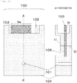
- an electrode structure which is an electrode 100 formed by resin molding a semiconductor device 103, includes a first resin mold portion formed on a front surface of the semiconductor device 103 and having a first thickness (t1), a second resin mold portion formed on a back surface of the semiconductor device 103 and having a second thickness (t2) greater than the first thickness, and an exposed portion 105 formed in a part of the first resin mold portion corresponding to an end of the semiconductor device.
- the insert-molding can be performed without destructing a semiconductor device such as a sensor and a memory.
- a semiconductor device such as a sensor and a memory.
- the embodiment has the following forms.
- the ion-selective electrode 100 includes a specimen flow path 101 and an external terminal 102 electrically connected to the specimen flow path 101 via an ion-selective membrane (not shown) .
- the flat semiconductor device 103 is molded with the resin 104.
- the semiconductor device 103 is, for example, a sensor or a memory.
- the thickness t1 of the front mold portion and the thickness t2 of the back mold portion of the semiconductor device 103 are different, and the end of the semiconductor device on the side of the smaller wall thickness is exposed at the exposed portion 105.
- the ion-selective electrode 100 of the first embodiment is an electrode formed by molding the semiconductor device 103 with the resin 104.
- the electrode 100 includes the first resin mold portion formed on the front surface of the semiconductor device 103 and having the first thickness (t1), and the second resin mold portion formed on the back surface of the semiconductor device 103 and having the second thickness (t2) greater than the first thickness.
- the electrode 100 includes the exposed portion 105 formed in a part of the first resin mold portion corresponding to the end of the semiconductor device 103.
- the exposed portion 105 is formed so that the mold resin cannot enter by contacting the mold during resin molding.
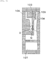
- FIG. 2 is a schematic diagram of a cross section of FIG. 1 taken along AA' during filling of the molten resin at the time of the insert-molding.
- a difference is provided between maximum wall thicknesses t1 and t2 on the front and back of the semiconductor device 103, and as shown in FIG. 2 , resin filling is promoted on a t2 side where the maximum wall thickness is greater.
- a speed at a resin tip end during filling is proportional to a cube of the wall thickness.
- a difference D between resin-filled regions occurs, and a bending force F due to a resin pressure acts from the t2 side with the larger maximum wall thickness toward a t1 side with a clamp end 109 as a fulcrum.
- the end on the t1 side having a smaller maximum wall thickness is supported by the mold 106. Therefore, displacement of the end of the semiconductor device 103 and bending deformation of the semiconductor device 103 can be prevented. Further, since both ends of the semiconductor device 103 are exposed, temperature control efficiency of the semiconductor device 103 (which generates heat during operation) using a blower or the like is improved. As a result, measurement accuracy of the ion-selective electrode 100 in which a potential measurement error with respect to temperature noise is large can be improved.
- the insert-molding was possible in the nondestructive manner. It is considered that this is because the large ratio of the cross-sectional width Tw to the thickness Ts strongly influences deformation of the semiconductor device 103 dominated by bending in a thickness direction, and high sensitivity of the speed of the resin tip end during filling to the wall thickness.
- the insert-molding was possible in the nondestructive manner. Further, the distance te from the end of the semiconductor device 103 to the end of the exposed portion 105 was smaller than the thickness ts (the minimum thickness for those with a distribution in thickness) of the semiconductor device 103. When the distance te was not smaller that the thickness ts, bending occurred on an end side of the semiconductor device 103 with respect to the exposed portion 105.
- the structure provides the resin gate 113, so that the shortest resin flow path (h1 + h2 of FIG. 6 ) to the t1 side with the smaller maximum wall thickness and the shortest resin flow path (h1' of FIG. 6 ) to the t2 side with a larger maximum wall thickness are equal, or the shortest resin flow path to the side with the larger average wall thickness becomes shorter.
- the molten resin 108 was more quickly and stably filled into the side with the larger average wall thickness, and nondestructive insert-molding was possible even when the maximum wall thickness difference was reduced to 10%.
- the shortest resin flow path is a sum of line segments from a center point of the gate 113 to end points of the front and back resin mold portions of the semiconductor device 103 through a mold cavity 107.
- the shortest resin flow path is also referred to as a shortest path when the end points of the resin mold portions of the semiconductor device 103 is stretched from the gate 113 in the mold cavity 107 with a thread.
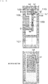
- a structure of an ion-selective electrode of the second embodiment will be described with reference to FIGS. 3A and 3B .
- a difference from the structure of the ion-selective electrode 100 of the first embodiment is that the protrusion 110 is provided at the end and the upper surface and a part of the side surface of the protrusion 110 are exposed.
- the other structure is almost the same as the structure of the ion-selective electrode 100 of the first embodiment, and the description thereof is omitted.
- the deformation of the semiconductor device 103 when the molten resin is filled can be further reduced. The reason for this will be described below.
- the protrusion 110 is caught (or by friction) and resistance is generated, and as a result, the displacement is further prevented.
- the protrusion 100 had a deformation preventing effect.
- a structure of an ion-selective electrode of the third embodiment will be described with reference to FIGS. 4A and 4B .
- a difference from the structure of the ion-selective electrode 100 of the first embodiment is that the spacer 111 whose softening temperature is equal to or higher than that of the mold resin is provided at the end of the semiconductor device 103 on a side having the smaller maximum wall thickness .
- the other structure is almost the same as the structure of the ion-selective electrode 100 of the first embodiment, and the description thereof is omitted.
- the bending force F due to the resin pressure when the molten resin is filled acts from the t2 side with the larger maximum wall thickness toward the t1 side with the clamp end as the fulcrum.
- the end on the t1 side with the smaller maximum wall thickness is supported by the mold 106 via the spacer 111 whose softening temperature is equal to or higher than that of the mold resin, displacement of the end of the semiconductor device 103 and bending deformation of the semiconductor device 103 can be prevented.
- the insert-molding was possible in the nondestructive manner.
- the insert-molding was possible in the nondestructive manner.
- a distance from the end of the semiconductor device 103 to an end of the spacer 111 was smaller than the thickness ts (the minimum thickness for those with a distribution in thickness) of the semiconductor device 103.
- a resin gate was provided, so that a shortest resin flow path to the t1 side with a smaller maximum wall thickness and a shortest resin flow path to the t2 side with a larger maximum wall thickness are equal, or a shortest resin flow path to the side with the larger maximum wall thickness becomes shorter.
- the resin was more quickly and stably filled into the side with the larger maximum wall thickness, and the nondestructive insert-molding was possible even when the maximum wall thickness difference was reduced to 10%.
- the semiconductor device 103 is not exposed, and a material of the spacer 111 is set to have a higher softening point than the mold resin, so that the semiconductor device 103 is not exposed.
- a risk of damage to the semiconductor device 103 due to direct contact with a rod or a pointed object is reduced, and the electrode 100 having excellent ion selectivity in terms of reliability can be obtained.
- Examples of the material of the spacer 111 include resin and ceramics.
- the convex portion or the concave portion 112 is provided on the front surface of the spacer 111, and a concave portion or a convex portion matching the convex portion or the concave portion 112 is provided on the mold 106.
- movement of the spacer 111 in a direction perpendicular to the thickness thereof can be restricted, and the positional deviation of the spacer 111 when the molten resin is filled can be prevented to improve the molding yield.
- the spacer 111 can be prevented from peeling off due to vibration, impact, or the like after the electrode housing is molded.
- the invention is not limited to the ion-selective electrode, but can be widely applied to semiconductor devices in which the semiconductor device 103 is insert-molded.
Landscapes
- Health & Medical Sciences (AREA)
- Life Sciences & Earth Sciences (AREA)
- Chemical & Material Sciences (AREA)
- General Physics & Mathematics (AREA)
- Physics & Mathematics (AREA)
- Electrochemistry (AREA)
- Pathology (AREA)
- Analytical Chemistry (AREA)
- Biochemistry (AREA)
- General Health & Medical Sciences (AREA)
- Molecular Biology (AREA)
- Immunology (AREA)
- Chemical Kinetics & Catalysis (AREA)
- Engineering & Computer Science (AREA)
- Theoretical Computer Science (AREA)
- Computer Hardware Design (AREA)
- Microelectronics & Electronic Packaging (AREA)
- Encapsulation Of And Coatings For Semiconductor Or Solid State Devices (AREA)
- Moulds For Moulding Plastics Or The Like (AREA)
- Structures Or Materials For Encapsulating Or Coating Semiconductor Devices Or Solid State Devices (AREA)
- Semiconductor Memories (AREA)
Applications Claiming Priority (2)
| Application Number | Priority Date | Filing Date | Title |
|---|---|---|---|
| JP2018075095A JP7117885B2 (ja) | 2018-04-10 | 2018-04-10 | 半導体装置 |
| PCT/JP2019/015335 WO2019198670A1 (ja) | 2018-04-10 | 2019-04-08 | 電極構造 |
Publications (2)
| Publication Number | Publication Date |
|---|---|
| EP3780073A1 true EP3780073A1 (de) | 2021-02-17 |
| EP3780073A4 EP3780073A4 (de) | 2021-12-29 |
Family
ID=68164128
Family Applications (1)
| Application Number | Title | Priority Date | Filing Date |
|---|---|---|---|
| EP19785253.6A Pending EP3780073A4 (de) | 2018-04-10 | 2019-04-08 | Elektrodenstruktur |
Country Status (5)
| Country | Link |
|---|---|
| US (1) | US11953461B2 (de) |
| EP (1) | EP3780073A4 (de) |
| JP (1) | JP7117885B2 (de) |
| CN (1) | CN111902921B (de) |
| WO (1) | WO2019198670A1 (de) |
Family Cites Families (17)
| Publication number | Priority date | Publication date | Assignee | Title |
|---|---|---|---|---|
| JPH042152A (ja) * | 1990-04-19 | 1992-01-07 | Mitsubishi Electric Corp | 樹脂封止型半導体装置及びその製造方法 |
| JPH04196141A (ja) * | 1990-11-26 | 1992-07-15 | Sony Corp | 半導体装置モールド方法 |
| JP2927660B2 (ja) * | 1993-01-25 | 1999-07-28 | シャープ株式会社 | 樹脂封止型半導体装置の製造方法 |
| US5690893A (en) | 1994-06-10 | 1997-11-25 | Hitachi, Ltd. | Analyzer having sensor with memory device |
| JP3564743B2 (ja) * | 1994-08-08 | 2004-09-15 | 日立化成工業株式会社 | 半導体素子封止用金型 |
| US5665653A (en) | 1995-03-29 | 1997-09-09 | Unifet, Incorporated | Method for encapsulating an electrochemical sensor |
| JPH09222413A (ja) * | 1996-02-16 | 1997-08-26 | Hitachi Ltd | 塩素イオンセンサ |
| JP2982952B2 (ja) * | 1996-03-21 | 1999-11-29 | 株式会社日立製作所 | 半導体装置 |
| JPH1187385A (ja) | 1997-09-10 | 1999-03-30 | Omron Corp | 樹脂モールド型電子部品の製造方法、成形金型、リードフレーム |
| WO2011034170A1 (ja) | 2009-09-18 | 2011-03-24 | 日立化成工業株式会社 | イオン選択性電極カートリッジ |
| JP2012151404A (ja) * | 2011-01-21 | 2012-08-09 | Yazaki Corp | 射出成形方法、射出成形装置及び電子装置 |
| JP2013050458A (ja) * | 2012-10-18 | 2013-03-14 | Hitachi Automotive Systems Ltd | 流量センサとその製造方法、及び流量センサモジュール |
| US20140132274A1 (en) | 2012-11-13 | 2014-05-15 | Awareness Technology Inc. | Method and apparatus for providing information in an electrolyte measurment system |
| JP6067498B2 (ja) * | 2013-07-08 | 2017-01-25 | 日立オートモティブシステムズ株式会社 | 流量センサ |
| US9281219B2 (en) * | 2013-09-18 | 2016-03-08 | Suprasensor Technologies, Llc | Molecular receptor-based chemical field-effect transistor (CHEMFET) devices, systems, and methods for in-situ nitrate monitoring in field soils |
| JP6678395B2 (ja) * | 2015-05-07 | 2020-04-08 | 株式会社日立ハイテク | イオンセンサ |
| JP6594431B2 (ja) * | 2015-08-20 | 2019-10-23 | 株式会社日立ハイテクノロジーズ | イオン濃度測定装置 |
-
2018
- 2018-04-10 JP JP2018075095A patent/JP7117885B2/ja active Active
-
2019
- 2019-04-08 US US17/045,826 patent/US11953461B2/en active Active
- 2019-04-08 EP EP19785253.6A patent/EP3780073A4/de active Pending
- 2019-04-08 WO PCT/JP2019/015335 patent/WO2019198670A1/ja not_active Ceased
- 2019-04-08 CN CN201980021113.0A patent/CN111902921B/zh active Active
Also Published As
| Publication number | Publication date |
|---|---|
| WO2019198670A1 (ja) | 2019-10-17 |
| JP2019186372A (ja) | 2019-10-24 |
| US11953461B2 (en) | 2024-04-09 |
| CN111902921A (zh) | 2020-11-06 |
| JP7117885B2 (ja) | 2022-08-15 |
| EP3780073A4 (de) | 2021-12-29 |
| CN111902921B (zh) | 2024-03-12 |
| US20210140913A1 (en) | 2021-05-13 |
Similar Documents
| Publication | Publication Date | Title |
|---|---|---|
| US8845966B2 (en) | Method for measuring analysis object and measuring device | |
| EP1455182B1 (de) | Ausfallbeurteilungsverfahren und analysierer | |
| US5821399A (en) | Automatic test parameters compensation of a real time fluid analysis sensing device | |
| CN101750160B (zh) | 用于监测测量单元的热耦合的方法 | |
| EP3067664B1 (de) | Sensor für rotationswinkelerfassung | |
| US20170350838A1 (en) | Electric measuring cartridge, biological sample electric measuring device, and biological sample electric measuring method | |
| EP2306182B1 (de) | Ionensensor, Ionensensormodul und Herstellungsverfahren für einen Ionensensor | |
| KR20150036605A (ko) | 사용되고 건조된 센서들을 검출하는 시스템 및 방법 | |
| JP2015148594A (ja) | 電気的測定用カートリッジ、並びに電気的測定装置及び電気的測定方法 | |
| US11953461B2 (en) | Electrode structure | |
| KR20060121710A (ko) | 검출 장치 및 그 제조 방법 | |
| JP6404049B2 (ja) | 流路一体型センサ | |
| US11892333B2 (en) | Flow-rate measuring device | |
| JP4901535B2 (ja) | 生体関連物質測定装置 | |
| JP2015169432A (ja) | 電気的測定用カートリッジ、並びに電気的測定装置及び電気的測定方法 | |
| JPH10197474A (ja) | 電気化学検出器用比較電極 | |
| JP3245687B2 (ja) | 熱放散定数の調整方法 | |
| CN112534287B (zh) | 传感器元件的安装结构、移动量检测装置及其制造方法 | |
| JP6876911B2 (ja) | 電気的測定用カートリッジ、電気的測定装置及び電気的測定方法 | |
| JP2000346731A (ja) | センサ | |
| CN118362912A (zh) | 电池传感器和用于制造电池传感器的方法 | |
| HK1141583B (en) | Method for monitoring the thermal coupling of measuring cell | |
| WO1995002827A1 (en) | Automatic test parameters compensation of a real time fluid analysis sensing device |
Legal Events
| Date | Code | Title | Description |
|---|---|---|---|
| STAA | Information on the status of an ep patent application or granted ep patent |
Free format text: STATUS: THE INTERNATIONAL PUBLICATION HAS BEEN MADE |
|
| PUAI | Public reference made under article 153(3) epc to a published international application that has entered the european phase |
Free format text: ORIGINAL CODE: 0009012 |
|
| STAA | Information on the status of an ep patent application or granted ep patent |
Free format text: STATUS: REQUEST FOR EXAMINATION WAS MADE |
|
| 17P | Request for examination filed |
Effective date: 20200928 |
|
| AK | Designated contracting states |
Kind code of ref document: A1 Designated state(s): AL AT BE BG CH CY CZ DE DK EE ES FI FR GB GR HR HU IE IS IT LI LT LU LV MC MK MT NL NO PL PT RO RS SE SI SK SM TR |
|
| AX | Request for extension of the european patent |
Extension state: BA ME |
|
| DAV | Request for validation of the european patent (deleted) | ||
| DAX | Request for extension of the european patent (deleted) | ||
| A4 | Supplementary search report drawn up and despatched |
Effective date: 20211129 |
|
| RIC1 | Information provided on ipc code assigned before grant |
Ipc: H01L 23/31 20060101ALN20211123BHEP Ipc: G06K 19/077 20060101ALI20211123BHEP Ipc: H01L 21/56 20060101ALI20211123BHEP Ipc: G06K 19/04 20060101ALI20211123BHEP Ipc: G01N 27/333 20060101AFI20211123BHEP |