EP3807367B1 - Formulation d'un matériau fonctionnel organique - Google Patents
Formulation d'un matériau fonctionnel organique Download PDFInfo
- Publication number
- EP3807367B1 EP3807367B1 EP19729300.4A EP19729300A EP3807367B1 EP 3807367 B1 EP3807367 B1 EP 3807367B1 EP 19729300 A EP19729300 A EP 19729300A EP 3807367 B1 EP3807367 B1 EP 3807367B1
- Authority
- EP
- European Patent Office
- Prior art keywords
- organic
- derivatives
- materials
- compounds
- formulation according
- Prior art date
- Legal status (The legal status is an assumption and is not a legal conclusion. Google has not performed a legal analysis and makes no representation as to the accuracy of the status listed.)
- Active
Links
Images


Classifications
-
- C—CHEMISTRY; METALLURGY
- C09—DYES; PAINTS; POLISHES; NATURAL RESINS; ADHESIVES; COMPOSITIONS NOT OTHERWISE PROVIDED FOR; APPLICATIONS OF MATERIALS NOT OTHERWISE PROVIDED FOR
- C09D—COATING COMPOSITIONS, e.g. PAINTS, VARNISHES OR LACQUERS; FILLING PASTES; CHEMICAL PAINT OR INK REMOVERS; INKS; CORRECTING FLUIDS; WOODSTAINS; PASTES OR SOLIDS FOR COLOURING OR PRINTING; USE OF MATERIALS THEREFOR
- C09D11/00—Inks
- C09D11/02—Printing inks
- C09D11/03—Printing inks characterised by features other than the chemical nature of the binder
- C09D11/033—Printing inks characterised by features other than the chemical nature of the binder characterised by the solvent
-
- C—CHEMISTRY; METALLURGY
- C09—DYES; PAINTS; POLISHES; NATURAL RESINS; ADHESIVES; COMPOSITIONS NOT OTHERWISE PROVIDED FOR; APPLICATIONS OF MATERIALS NOT OTHERWISE PROVIDED FOR
- C09D—COATING COMPOSITIONS, e.g. PAINTS, VARNISHES OR LACQUERS; FILLING PASTES; CHEMICAL PAINT OR INK REMOVERS; INKS; CORRECTING FLUIDS; WOODSTAINS; PASTES OR SOLIDS FOR COLOURING OR PRINTING; USE OF MATERIALS THEREFOR
- C09D11/00—Inks
- C09D11/30—Inkjet printing inks
- C09D11/36—Inkjet printing inks based on non-aqueous solvents
-
- C—CHEMISTRY; METALLURGY
- C09—DYES; PAINTS; POLISHES; NATURAL RESINS; ADHESIVES; COMPOSITIONS NOT OTHERWISE PROVIDED FOR; APPLICATIONS OF MATERIALS NOT OTHERWISE PROVIDED FOR
- C09D—COATING COMPOSITIONS, e.g. PAINTS, VARNISHES OR LACQUERS; FILLING PASTES; CHEMICAL PAINT OR INK REMOVERS; INKS; CORRECTING FLUIDS; WOODSTAINS; PASTES OR SOLIDS FOR COLOURING OR PRINTING; USE OF MATERIALS THEREFOR
- C09D11/00—Inks
- C09D11/30—Inkjet printing inks
- C09D11/38—Inkjet printing inks characterised by non-macromolecular additives other than solvents, pigments or dyes
-
- C—CHEMISTRY; METALLURGY
- C09—DYES; PAINTS; POLISHES; NATURAL RESINS; ADHESIVES; COMPOSITIONS NOT OTHERWISE PROVIDED FOR; APPLICATIONS OF MATERIALS NOT OTHERWISE PROVIDED FOR
- C09D—COATING COMPOSITIONS, e.g. PAINTS, VARNISHES OR LACQUERS; FILLING PASTES; CHEMICAL PAINT OR INK REMOVERS; INKS; CORRECTING FLUIDS; WOODSTAINS; PASTES OR SOLIDS FOR COLOURING OR PRINTING; USE OF MATERIALS THEREFOR
- C09D11/00—Inks
- C09D11/50—Sympathetic, colour changing or similar inks
-
- C—CHEMISTRY; METALLURGY
- C09—DYES; PAINTS; POLISHES; NATURAL RESINS; ADHESIVES; COMPOSITIONS NOT OTHERWISE PROVIDED FOR; APPLICATIONS OF MATERIALS NOT OTHERWISE PROVIDED FOR
- C09D—COATING COMPOSITIONS, e.g. PAINTS, VARNISHES OR LACQUERS; FILLING PASTES; CHEMICAL PAINT OR INK REMOVERS; INKS; CORRECTING FLUIDS; WOODSTAINS; PASTES OR SOLIDS FOR COLOURING OR PRINTING; USE OF MATERIALS THEREFOR
- C09D11/00—Inks
- C09D11/52—Electrically conductive inks
-
- H—ELECTRICITY
- H10—SEMICONDUCTOR DEVICES; ELECTRIC SOLID-STATE DEVICES NOT OTHERWISE PROVIDED FOR
- H10K—ORGANIC ELECTRIC SOLID-STATE DEVICES
- H10K71/00—Manufacture or treatment specially adapted for the organic devices covered by this subclass
- H10K71/10—Deposition of organic active material
- H10K71/12—Deposition of organic active material using liquid deposition, e.g. spin coating
- H10K71/13—Deposition of organic active material using liquid deposition, e.g. spin coating using printing techniques, e.g. ink-jet printing or screen printing
- H10K71/135—Deposition of organic active material using liquid deposition, e.g. spin coating using printing techniques, e.g. ink-jet printing or screen printing using ink-jet printing
-
- H—ELECTRICITY
- H10—SEMICONDUCTOR DEVICES; ELECTRIC SOLID-STATE DEVICES NOT OTHERWISE PROVIDED FOR
- H10K—ORGANIC ELECTRIC SOLID-STATE DEVICES
- H10K71/00—Manufacture or treatment specially adapted for the organic devices covered by this subclass
- H10K71/10—Deposition of organic active material
- H10K71/12—Deposition of organic active material using liquid deposition, e.g. spin coating
- H10K71/15—Deposition of organic active material using liquid deposition, e.g. spin coating characterised by the solvent used
-
- H—ELECTRICITY
- H10—SEMICONDUCTOR DEVICES; ELECTRIC SOLID-STATE DEVICES NOT OTHERWISE PROVIDED FOR
- H10K—ORGANIC ELECTRIC SOLID-STATE DEVICES
- H10K50/00—Organic light-emitting devices
- H10K50/10—OLEDs or polymer light-emitting diodes [PLED]
- H10K50/17—Carrier injection layers
Definitions
- the present invention relates to a formulation as defined in claim 1 containing at least one organic functional material and at least three different organic solvents, selected from at least two different organic solvents A and at least one organic solvent B, as well as to electroluminescent devices prepared by using these formulations.
- OLEDs Organic Light Emitting Devices
- Other techniques such as inkjet printing have been recently thoroughly investigated because of their advantages such as cost savings and scale-up possibilities.
- One of the main challenges in multi-layer printing is to identify the relevant parameters to obtain a homogeneous deposition of inks on the substrate. To trigger these parameters, such as surface tension, viscosity or boiling point, some additives can be added to the formulation.
- One object of the present invention is to provide a formulation of an organic semiconductor which allows a controlled deposition to form organic semiconductor layers having good properties and efficient performance.
- a further object of the present invention is to provide a formulation of an organic semiconductor which allows an excellent film uniformity when deposited and dried on a substrate using e.g. an inkjet printing method thereby giving good layer properties and efficient performance.
- a solute composed of the constituent material or its precursor of the functional layer, dissolved in a first and second solvent, wherein the first solvent has a first solubility parameter and a first boiling point and the second solvent has a smaller second solubility parameter than the first solubility parameter and a second lower boiling point than the first boiling point, the first boiling point is ⁇ 250°C and the second boiling point is ⁇ 170°C, the difference between the second and the first boiling point is ⁇ 40°C and the second solubility parameter is 9.0 (cal/cm 3 ) 1/2 or less.
- an ink for functional layer formation comprising a first component that is a solute, a second component that has a boiling point in the range from 280 to 350°C, is a good solvent for the first component, and is at least one type selected from the group consisting of an aromatic hydrocarbon including at least two aromatic rings, aromatic glycol ether, aliphatic glycol ether, aliphatic acetate, and aliphatic ester, and a third component that has a boiling point in the range from 200 to 300°C, is a good solvent for the first component, and is at least one type selected from the group consisting of an aromatic hydrocarbon, an aromatic ether, and an aliphatic ether, wherein the proportion of the second component in a mixed solvent including the second component and the third component is 10 wt% or greater.
- a function layer ink for forming a functional layer by a liquid coating method wherein the function layer material contains a macromolecular or low-molecular-weight material, and a mixed solvent containing 0.1 % by weight or more of solvent A having a viscosity in the range from 0.01 to 0.05 Pas, and solvent B having a viscosity of less than 0.01 Pas and a lower boiling point than the solvent A, the mixed solvent has a viscosity of less than 0.02 Pas and a boiling point in the range from 200 to 350°C.
- solutions of at least one organic semiconductor containing at least one high-molecular weight constituent in a solvent mixture of at least three different solvents A, B and C are disclosed.
- Solvents A and B are good solvents for the organic semiconductor
- the solvent C is a bad solvent for the organic semiconductor.
- compositions comprising at least one organic semiconductor which comprises at least one high-molecular-weight component, and at least one organic solvent A which is a good solvent for the organic semiconductor, and at least one organic solvent B which is a poor solvent for the organic semiconductor, characterised in that the following applies to the boiling points (b.p.) of solvents A and B: b.p.(A) > b.p.(B).
- a formulation as defined in claim 1 comprising at least one organic functional material and at least three different organic solvents, selected from at least two different organic solvents A and at least one organic solvent B.
- the inventors have surprisingly found that the use of the formulations of the present invention allows an effective ink deposition to form uniform and well-defined organic layers of functional materials which have good performance. More specifically, the formulations of the present invention lead to a very flat layer profile within the pixel and to a reduced material accumulation (also called pile-up) at the border of the pixel. Absence of pile-up in this pixel area is a very strong asset, especially e.g. for applications in top-emission devices.
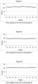
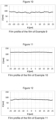
- Figures 1 to 17 show the film profiles of the films prepared in the Reference Example ( Fig. 1 ), the working examples 1 to 13 ( Fig. 2 to 14 ), the comparative examples 1 and 2 ( Fig. 15 and 16 ) as well as in the working example 14 ( Fig. 17 ).
- the present invention relates to a formulation containing at least one organic functional material and at least three different organic solvents, selected from at least two different organic solvents A and at least one organic solvent B, characterized in that at least one of the first organic solvents A has a boiling point in the range from 250 to 350°C and a viscosity of ⁇ 15 mPas, the second organic solvent B has a boiling point in the range from 200 to 350°C and a viscosity of ⁇ 10 mPas and the solubility of the at least one organic functional material in the second organic solvent B is ⁇ 5 g/l.
- the formulation is characterized in that at least two of the organic solvents A have a boiling point in the range from 250 to 350°C and a viscosity of ⁇ 15 mPas.
- the formulation is characterized in that at least one of the organic solvents A is selected from naphthalene derivatives, partially hydrogenated naphthalene derivatives, e.g. tetrahydronaphthalene derivatives, fully hydrogenated naphthalene derivatives, e.g. decahydronapthalene derivatives, indane derivatives and fully hydrogenated anthracene derivatives having a viscosity of ⁇ 15 mPas.
- the organic solvents A is selected from naphthalene derivatives, partially hydrogenated naphthalene derivatives, e.g. tetrahydronaphthalene derivatives, fully hydrogenated naphthalene derivatives, e.g. decahydronapthalene derivatives, indane derivatives and fully hydrogenated anthracene derivatives having a viscosity of ⁇ 15 mPas.
- the formulation is characterized in that at least two of the organic solvents A are selected from naphthalene derivatives, partially hydrogenated naphthalene derivatives, fully hydrogenated naphthalene derivatives, indane derivatives and fully hydrogenated anthracene derivatives having a viscosity of ⁇ 15 mPas.
- the expression "derivatives" as used above and below in the present application means that the core structure, e.g. the naphthalene core or the partially/fully hydrogenated naphthalene core, is substituted at least by one substituent R.
- R is identical or different at each occurence, either
- the formulation is characterized in that at least one of the organic solvents A is selected from naphthalene derivatives, tetrahydronaphthalene derivatives and decahydronaphthalene derivatives having a viscosity of ⁇ 15 mPas.
- the formulation is characterized in that at least two of the organic solvents A are selected from naphthalene derivatives, tetrahydronaphthalene derivatives and decahydronaphthalene derivatives having a viscosity of ⁇ 15 mPas.
- At least one organic solvent A is a naphthalene derivative, it is preferably a solvent according to general formula (I) wherein
- the naphthalene derivative is either 1-cyclohexyl-naphthalene or 1-phenyl-naphthalene.
- At least one organic solvent A is a tetrahydronaphthalene derivative, it is preferably a solvent according to general formula (II) or (III) wherein R can have the meanings as given above with respect to formula (I).
- the tetrahydronaphthalene derivative is 1-phenyl-1,2,3,4-tetrahydronaphthalene.
- At least one organic solvent A is a decahydronaphthalene derivative, it is preferably a solvent according to general formula (IV) wherein R can have the meanings as given above with respect to formula (I).
- the decahydronaphthalene derivative is either 1-cyclohexyl-decahydronaphthalene or 1-phenyl-decahydronaphthalene.
- At least one of the organic solvents A has a boiling point in the range from 250 to 350°C, preferably in the range from 260 to 340°C and most preferably in the range from 270 to 330°C.
- the total content of the at least two different organic solvents A is from 0,1 to 50 vol.-%, more preferably from 0,1 to ⁇ 40 vol.-%, based on the total amount of organic solvents in the formulation.
- the content of each of the at least two different organic solvents A is from 0,1 to 40 vol.-%.
- the viscosity of at least one organic solvent A is ⁇ 15 mPas.
- the viscosity of at least one solvent A is preferably ⁇ 20 mPas, more preferably ⁇ 25 mPas and most preferably ⁇ 50 mPas.
- the formulations of the present invention comprise at least one organic solvent B which is different from the organic solvents A.
- the organic solvent B is employed together with the at least two organic solvents A.
- Suitable organic solvents B are preferably organic solvents which include inter alia, ketones, ethers, esters, amides such as di-C 1-2 -alkylformamides, sulfur compounds, nitro compounds, hydrocarbons, halogenated hydrocarbons (e.g. chlorinated hydrocarbons), aromatic or heteroaromatic hydrocarbons (e.g. naphthalene derivatives) and halogenated aromatic or heteroaromatic hydrocarbons.
- organic solvents which include inter alia, ketones, ethers, esters, amides such as di-C 1-2 -alkylformamides, sulfur compounds, nitro compounds, hydrocarbons, halogenated hydrocarbons (e.g. chlorinated hydrocarbons), aromatic or heteroaromatic hydrocarbons (e.g. naphthalene derivatives) and halogenated aromatic or heteroaromatic hydrocarbons.
- the second organic solvent B can be chosen from one of the following groups: substituted and non-substituted, aromatic or aliphatic, cyclic or linear ethers such as 3-phenoxytoluene or anisole; substituted or non-substituted arene derivatives such as cyclohexylbenzene; substituted or non-substituted indanes; substituted and non-substituted, aromatic or aliphatic, cyclic or linear ketones such as dicyclohexylmethanone; substituted and non-substituted heterocycles such as pyrrolidinones, pyridines, pyrazines; other fluorinated or chlorinated aromatic hydrocarbons, substituted or non-substituted naphthalenes such as alkyl substituted naphthalenes, such as 1-ethyl naphthalene.
- Particularly preferred second organic solvents B are, for example, 1-ethyl-naphthalene, 2-ethylnaphthalene, 2-propylnaphthalene, 2-(1-methylethyl)-naphthalene, 1-(1-methylethyl)-naphthalene, 1,6-dimethylnaphthalene, 2,2'-dimethylbiphenyl, 3,3'-dimethylbiphenyl, 1 -acetylnaphthalene,1,2,3,4-tetramethylbenzene, 1,2,3,5-tetramethyl-benzene, 1,2,4,5-tetramethylbenzene, 1,2,4-trichlorobenzene, 1,2-dihydronaphthalene, 1,2-dimethylnaphthalene, 1,3-benzodioxole, 1,3-diisopropylbenzene, 1,3-dimethylnaphthalene, 1,4-benzodioxane,
- the organic solvent B has a boiling point in the range from 200 to 350°C, preferably in the range from 225 to 325°C and most preferably in the range from 250 to 300°C.
- the content of the at least one organic solvent B is preferably in the range from 50 to 99,9 vol.-%, more preferably in the range from 60 to 99,9 vol.-%, based on the total amount of organic solvents in the formulation.
- the at least one organic functional material has a solubility in the at least one organic solvent B which is ⁇ 5 g/l, preferably ⁇ 10 g/l.
- Table 2 Preferred organic solvents B and their boiling points (BP) and melting points (MP) at 760 mm Hg.
- Solvent B BP (°C) MP(°C) CAS 3586-14-9 3-Phenoxytoluene 271 Liquid at RT CAS 136-60-7 Butylbenzoate 249 Liquid at RT CAS 827-52-1 Cyclohexylbenzene 239 Liquid at RT CAS 1127-76-0 1-Ethylnaphthalene 258 -15 CAS 7774-44-9 Cyclohexylisovalerate 223 Liquid at RT CAS 16409-46-4 Menthylisovalerate 270 Liquid at RT CAS 6243-10-3 Cyclohexylhexanoate 255 Liquid at RT CAS 103-93-5 p -Tolylisobutyrate 237 Liquid at RT CAS 605-39-0 2,2'-Dimethylbiphenyl 259 18 CAS 571-58-4 1,4-Dimethylnaphthalene 267 -18 CAS 612-75-9 3,3
- the formulations of the present application optionally can comprise at least a further organic solvent C which is different from the organic solvents A and B.
- the at least one organic solvent C is employed together with the at least two organic solvents A and the at least one organic solvent B.
- Suitable organic solvents C are preferably organic solvents which include inter alia, ketones, ethers, esters, amides such as di-C 1-2 -alkylformamides, sulfur compounds, nitro compounds, hydrocarbons, halogenated hydrocarbons, aromatic or heteroaromatic hydrocarbons and halogenated aromatic or heteroaromatic hydrocarbons.
- the organic solvent C can be chosen from one of the following groups: substituted and non-substituted, aromatic or aliphatic, cyclic or linear ethers, such as 3-phenoxytoluene or anisole; substituted or non-substituted arene derivatives such as cyclohexylbenzene or pentylbenzene; substituted or non-substituted indanes; substituted and non-substituted aromatic or aliphatic, cyclic or linear ketones, such as dicyclohexylmethanone; substituted and non-substituted heterocycles such as pyrrolidinones, pyridines, pyrazines; other fluorinated or chlorinated aromatic hydrocarbons, substituted or non-substituted naphthalenes such as alkyl substituted naphthalenes.
- substituted and non-substituted, aromatic or aliphatic, cyclic or linear ethers such as
- organic solvents C are, for example, pentyl benzene, hexylbenzene, heptylbenzene, octylbenzene, nonylbenzene, decylbenzene, 1-ethyl-naphthalene, 2-ethylnaphthalene, 2-propylnaphthalene, 2-(1-methylethyl)-naphthalene, 1-(1-methylethyl)-naphthalene, 2-butyl naphthalene, 1,6-dimethylnaphthalene, 2,2'-dimethylbiphenyl, 3,3'-dimethylbiphenyl, 1 -acetylnaphthalene,1,2,3,4-tetramethylbenzene, 1,2,3,5-tetramethyl-benzene, 1,2,4,5-tetramethylbenzene, 1,2,4-trichlorobenzene, 1,2-dihydronaphthalene,
- the organic solvent C has a boiling point in the range from 150 to 300°C, preferably in the range from 175 to 275°C and most preferably in the range from 200 to 250°C.
- the boiling point of solvent C is lower than the boiling point of the at least one solvent B, preferably at least 10°C lower, more preferably at least 20°C lower.
- the content of the at least one organic solvent C is preferably in the range from 0 to 30 vol.-%, more preferably in the range from 1 to 25 vol.-%, and most preferably in the range from 5 to 20 vol.-%, based on the total amount of organic solvents in the formulation.
- the content of the at least one organic functional material in the formulation is in the range from 0.001 to 20 weight-%, preferably in the range from 0.01 to 10 weight-%, more preferably in the range from 0.1 to 5 weight-% and most preferably in the range from 0.3 to 5 weight-%, based on the total weight of the formulation.
- the formulation of the present invention has a viscosity preferably in the range from 0.8 to 50 mPas, more preferably in the range from 1 to 40 mPas, and most preferably in the range from 1 to 15 mPas.
- the viscosity of the formulations and solvents according to the present invention is measured with a 1° cone-plate rotational rheometer of the type Discovery AR3 (Thermo Scientific). The equipment allows a precise control of the temperature and sheer rate. Measurement of viscosity is carried out at a temperature of 25.0°C (+/- 0.2°C) and a sheer rate of 500 s -1 . Each sample is measured three times and the obtained values are averaged.
- the formulation of the present invention has a surface tension preferably in the range from 10 to 70 mN/m, more preferably in the range from 15 to 50 mN/m and most preferably in the range from 20 to 40 mN/m.
- the organic solvent blend comprises a surface tension in the range from 10 to 70 mN/m, more preferably in the range from 15 to 50 mN/m and most preferably in the range from 20 to 40 mN/m.
- the surface tension can be measured using a FTA (First Ten Angstrom) 1000 contact angle goniometer at 20°C. Details of the method are available from First Ten Angstrom as published by Roger P. Woodward, Ph.D. "Surface Tension Measurements Using the Drop Shape Method" .
- the pendant drop method can be used to determine surface tension. This measurement technique dispenses a drop from a needle in a bulk liquid or gaseous phase. The droplet shape results from the relationship between surface-tension, gravity and density differences.
- surface tension is calculated from the shadow image of a pendant drop using http://www.kruss.de/services/education-theory/glossary/drop-shape-analysis.
- a commonly used and commercially available high precision drop shape analysis tool namely FTA1000 from First Ten Angstrom, was used to perform all surface tension measurements.
- Surface tension is determined by the software FTA1000. All measurements were performed at room temperature which is in the range between 20°C and 25°C.
- the procedure includes determination of the surface tension of each formulation using a fresh disposable drop dispensing system (syringe and needle). Each drop is measured over the duration of one minute with sixty measurements which are later on averaged. For each formulation three drops are measured. The final value is averaged over said measurements.
- the tool is regularly cross-checked against various liquids having well known surface tensions.
- the formulation according to the present invention comprises at least one organic functional material which can be employed for the production of functional layers of electronic devices.
- Functional materials are generally the organic materials which are introduced between the anode and the cathode of an electronic device.
- organic functional material denotes, inter alia, organic conductors, organic semiconductors, organic fluorescent compounds, organic phosphorescent compounds, organic light-absorbent compounds, organic light-sensitive compounds, organic photosensitisation agents and other organic photoactive compounds.
- organic functional material furthermore encompasses organometallic complexes of transition metals, rare earths, lanthanides and actinides.
- the organic functional material is selected from the group consisting of fluorescent emitters, phosphorescent emitters, host materials, matrix materials, exciton-blocking materials, electron-transport materials, electron-injection materials, hole-conductor materials, hole-injection materials, n-dopants, p-dopants, wide-band-gap materials, electron-blocking materials and hole-blocking materials.
- the organic functional material is an organic semiconductor selected from the group consisting of hole-injecting, hole-transporting, emitting, electron-transporting and electron-injecting materials.
- the organic functional material can be a compound having a low molecular weight, a polymer, an oligomer or a dendrimer, where the organic functional material may also be in the form of a mixture.
- the formulations according to the present invention may comprise two or more different compounds having a low molecular weight, one compound having a low molecular weight and one polymer or two polymers (blend).
- Organic functional materials are frequently described via the properties of the frontier orbitals, which are described in greater detail below.
- Molecular orbitals in particular also the highest occupied molecular orbital (HOMO) and the lowest unoccupied molecular orbital (LUMO), their energy levels and the energy of the lowest triplet state T 1 or of the lowest excited singlet state S 1 of the materials can be estimated based on quantum-chemical calculations.
- HOMO highest occupied molecular orbital
- LUMO lowest unoccupied molecular orbital
- their energy levels and the energy of the lowest triplet state T 1 or of the lowest excited singlet state S 1 of the materials can be estimated based on quantum-chemical calculations.
- a geometry optimisation is carried out using the "Ground State/Semi-empirical/Default Spin/AM1/Charge 0/Spin Singlet" method.
- An energy calculation is subsequently carried out on the basis of the optimised geometry.
- the "TD-SCF/DFT/Default Spin/B3PW91" method with the "6-31G(d)" base set (charge 0, spin singlet) is used here.
- the geometry is optimised via the "Ground State/Hartree-Fock/Default Spin/LanL2MB/Charge 0/Spin Singlet” method.
- the energy calculation is carried out analogously to the above-described method for the organic substances, with the difference that the "LanL2DZ" base set is used for the metal atom and the "6-31G(d)" base set is used for the ligands.
- the energy calculation gives the HOMO energy level HEh or LUMO energy level LEh in hartree units.
- these values are to be regarded as HOMO and LUMO energy levels respectively of the materials.
- the lowest triplet state T 1 is defined as the energy of the triplet state having the lowest energy which arises from the quantum-chemical calculation described.
- the lowest excited singlet state S 1 is defined as the energy of the excited singlet state having the lowest energy which arises from the quantum-chemical calculation described.
- a hole-injection material has an HOMO level which is in the region of or above the level of the anode, i.e. in general is at least -5.3 eV.
- hole-transport materials are capable of transporting holes, i.e. positive charges, which are generally injected from the anode or an adjacent layer, for example a hole-injection layer.
- a hole-transport material generally has a high HOMO level of preferably at least -5.4 eV.
- phenylenediamine derivatives US 3615404
- arylamine derivatives US 3567450
- amino-substituted chalcone derivatives US 3526501
- styrylanthracene derivatives JP-A-56-46234
- polycyclic aromatic compounds EP 1009041
- polyarylalkane derivatives US 3615402
- fluorenone derivatives JP-A-54-110837
- hydrazone derivatives US 3717462
- acylhydrazones stilbene derivatives
- silazane derivatives US 4950950
- polysilanes JP-A-2-204996
- aniline copolymers JP-A-2-282263
- thiophene oligomers JP Heisei 1 (1989) 211399
- polythiophenes polythiophenes
- arylamine dendrimers JP Heisei 8 (1996) 193191
- monomeric triarylamines US 3180730
- triarylamines containing one or more vinyl radicals and/or at least one functional group containing active hydrogen US 3567450 and US 3658520
- tetraaryldiamines the two tertiary amine units are connected via an aryl group.
- More triarylamino groups may also be present in the molecule.
- Phthalocyanine derivatives such as, for example, dipyrazino[2,3-f:2',3'-h]quinoxalinehexacarbonitrile, are also suitable.
- arylamines and heterocycles which are generally employed as hole-injection and/or hole-transport materials preferably result in an HOMO in the polymer of greater than -5.8 eV (vs. vacuum level), particularly preferably greater than -5.5 eV.
- LUMO lowest unoccupied molecular orbital
- Particularly suitable compounds for electron-transporting and electron-injecting layers are metal chelates of 8-hydroxyquinoline (for example LiQ, AlQ 3 , GaQ 3 , MgQ 2 , ZnQ 2 , InQ 3 , ZrQ 4 ), BAlQ, Ga oxinoid complexes, 4-azaphenanthren-5-ol-Be complexes ( US 5529853 A , cf. formula ET-1), butadiene derivatives ( US 4356429 ), heterocyclic optical brighteners ( US 4539507 ), benzimidazole derivatives ( US 2007/0273272 A1 ), such as, for example, TPBI ( US 5766779 , cf.
- 8-hydroxyquinoline for example LiQ, AlQ 3 , GaQ 3 , MgQ 2 , ZnQ 2 , InQ 3 , ZrQ 4
- BAlQ Ga oxinoid complexes
- 4-azaphenanthren-5-ol-Be complexes US 5
- 1,3,5-triazines for example spirobifluorenyltriazine derivatives (for example in accordance with DE 102008064200 ), pyrenes, anthracenes, tetracenes, fluorenes, spiro-fluorenes, dendrimers, tetracenes (for example rubrene derivatives), 1,10-phenanthroline derivatives ( JP 2003-115387 , JP 2004-311184 , JP 2001-267080 , WO 02/043449 ), silacyclopentadiene derivatives ( EP 1480280 , EP 1478032 , EP 1469533 ), borane derivatives, such as, for example, tri-arylborane derivatives containing Si ( US 2007/0087219 A1 , cf.
- formula ET-3 pyridine derivatives ( JP 2004-200162 ), phenanthrolines, especially 1,10-phenanthroline derivatives, such as, for example, BCP and Bphen, also several phenanthrolines connected via biphenyl or other aromatic groups ( US 2007-0252517 A1 ) or phenanthrolines connected to anthracene ( US 2007-0122656 A1 , cf. formulae ET-4 and ET-5).
- phenanthrolines especially 1,10-phenanthroline derivatives, such as, for example, BCP and Bphen, also several phenanthrolines connected via biphenyl or other aromatic groups ( US 2007-0252517 A1 ) or phenanthrolines connected to anthracene ( US 2007-0122656 A1 , cf. formulae ET-4 and ET-5).
- heterocyclic organic compounds such as, for example, thiopyran dioxides, oxazoles, triazoles, imidazoles or oxadiazoles.
- heterocyclic organic compounds such as, for example, thiopyran dioxides, oxazoles, triazoles, imidazoles or oxadiazoles.
- five-membered rings containing N such as, for example, oxazoles, preferably 1,3,4-oxadiazoles, for example compounds of the formulae ET-6, ET-7, ET-8 and ET-9, which are disclosed, inter alia, in US 2007/0273272 A1 ; thiazoles, oxadiazoles, thiadiazoles, triazoles, inter alia, see US 2008/0102311 A1 and Y.A. Levin, M.S.
- organic compounds such as fluorenones, fluorenylidenemethanes, perylenetetracarbonic acids, anthraquinone-dimethanes, diphenoquinones, anthrones and anthraquinonediethylene-diamines and derivatives thereof.
- the compounds which are able to generate electron-injection and/or electron-transport properties preferably result in an LUMO of less than -2.5 eV (vs. vacuum level), particularly preferably less than -2.7 eV.
- the present formulations may comprise emitters.
- emitter denotes a material which, after excitation, which can take place by transfer of any type of energy, allows a radiative transition into a ground state with emission of light.
- two classes of emitter are known, namely fluorescent and phosphorescent emitters.
- fluorescent emitter denotes materials or compounds in which a radiative transition from an excited singlet state into the ground state takes place.
- phosphorescent emitter preferably denotes luminescent materials or compounds which contain transition metals.
- Emitters are frequently also called dopants if the dopants cause the properties described above in a system.
- a dopant in a system comprising a matrix material and a dopant is taken to mean the component whose proportion in the mixture is the smaller.
- a matrix material in a system comprising a matrix material and a dopant is taken to mean the component whose proportion in the mixture is the greater.
- the term phosphorescent emitter can also be taken to mean, for example, phosphorescent dopant.
- Compounds which are able to emit light include, inter alia, fluorescent emitters and phosphorescent emitters. These include, inter alia, compounds containing stilbene, stilbenamine, styrylamine, coumarine, rubrene, rhodamine, thiazole, thiadiazole, cyanine, thiophene, paraphenylene, perylene, phtalocyanine, porphyrin, ketone, quinoline, imine, anthracene and/or pyrene structures. Particular preference is given to compounds which are able to emit light from the triplet state with high efficiency, even at room temperature, i.e. exhibit electrophosphorescence instead of electro-fluorescence, which frequently causes an increase in the energy efficiency.
- Suitable for this purpose are firstly compounds which contain heavy atoms having an atomic number of greater than 36. Preference is given to compounds which contain d- or f-transition metals which satisfy the above-mentioned condition. Particular preference is given here to corresponding compounds which contain elements from group 8 to 10 (Ru, Os, Rh, Ir, Pd, Pt).
- Suitable functional compounds here are, for example, various complexes, as described, for example, in WO 02/068435 A1 , WO 02/081488 A1 , EP 1239526 A2 and WO 2004/026886 A2 .
- Preferred compounds which can serve as fluorescent emitters are described by way of example below.
- Preferred fluorescent emitters are selected from the class of the monostyrylamines, the distyrylamines, the tristyrylamines, the tetrastyrylamines, the styrylphosphines, the styryl ethers and the arylamines.
- a monostyrylamine is taken to mean a compound which contains one substituted or unsubstituted styryl group and at least one, preferably aromatic, amine.
- a distyrylamine is taken to mean a compound which contains two substituted or unsubstituted styryl groups and at least one, preferably aromatic, amine.
- a tristyrylamine is taken to mean a compound which contains three substituted or unsubstituted styryl groups and at least one, preferably aromatic, amine.
- a tetrastyrylamine is taken to mean a compound which contains four substituted or unsubstituted styryl groups and at least one, preferably aromatic, amine.
- the styryl groups are particularly preferably stilbenes, which may also be further substituted.
- Corresponding phosphines and ethers are defined analogously to the amines.
- An arylamine or an aromatic amine in the sense of the present invention is taken to mean a compound which contains three substituted or unsubstituted aromatic or heteroaromatic ring systems bonded directly to the nitrogen. At least one of these aromatic or heteroaromatic ring systems is preferably a condensed ring system, preferably having at least 14 aromatic ring atoms.
- aromatic anthracenamines are taken to mean a compound in which one diarylamino group is bonded directly to an anthracene group, preferably in the 9-position.
- aromatic anthracenediamine is taken to mean a compound in which two diarylamino groups are bonded directly to an anthracene group, preferably in the 2,6- or 9,10-position.
- Aromatic pyrenamines, pyrenediamines, chrysenamines and chrysenediamines are defined analogously thereto, where the diarylamino groups are preferably bonded to the pyrene in the 1-position or in the 1,6-position.
- fluorescent emitters are selected from indenofluoren-amines or indenofluorenediamines, which are described, inter alia, in WO 2006/122630 ; benzoindenofluorenamines or benzoindenofluorenedi-amines, which are described, inter alia, in WO 2008/006449 ; and dibenzo-indenofluorenamines or dibenzoindenofluorenediamines, which are described, inter alia, in WO 2007/140847 .
- Examples of compounds from the class of the styrylamines which can be employed as fluorescent emitters are substituted or unsubstituted tristilben-amines or the dopants described in WO 2006/000388 , WO 2006/058737 , WO 2006/000389 , WO 2007/065549 and WO 2007/115610 .
- Distyryl-benzene and distyrylbiphenyl derivatives are described in US 5121029 . Further styrylamines can be found in US 2007/0122656 A1 .
- Particularly preferred styrylamine compounds are the compounds of the formula EM-1 described in US 7250532 B2 and the compounds of the formula EM-2 described in DE 10 2005 058557 A1 :
- triarylamine compounds are compounds of the formulae EM-3 to EM-15 disclosed in CN 1583691 A , JP 08/053397 A and US 6251531 B1 , EP 1957606 A1 , US 2008/0113101 A1 , US 2006/210830 A , WO 2008/006449 and DE 102008035413 and derivatives thereof:
- Further preferred compounds which can be employed as fluorescent emitters are selected from derivatives of naphthalene, anthracene, tetracene, benzanthracene, benzophenanthrene ( DE 10 2009 005746 ), fluorene, fluoranthene, periflanthene, indenoperylene, phenanthrene, perylene ( US 2007/0252517 A1 ), pyrene, chrysene, decacyclene, coronene, tetraphenylcyclopentadiene, pentaphenylcyclopentadiene, fluorene, spirofluorene, rubrene, coumarine ( US 4769292 , US 6020078 , US 2007/ 0252517 A1 ), pyran, oxazole, benzoxazole, benzothiazole, benzimidazole, pyrazine, cinnamic acid esters, diketopyrrol
- anthracene compounds particular preference is given to 9,10-substituted anthracenes, such as, for example, 9,10-diphenylanthracene and 9,10-bis(phenylethynyl)anthracene.
- 9,10-substituted anthracenes such as, for example, 9,10-diphenylanthracene and 9,10-bis(phenylethynyl)anthracene.
- 1,4-Bis(9'-ethynylanthracenyl)-benzene is also a preferred dopant.
- DMQA N,N'-dimethylquinacri-done
- thiopyran polymethine
- pyrylium and thiapyrylium salts periflanthene and
- Blue fluorescent emitters are preferably polyaromatic compounds, such as, for example, 9,10-di(2-naphthylanthracene) and other anthracene derivatives, derivatives of tetracene, xanthene, perylene, such as, for example, 2,5,8,11-tetra-t-butylperylene, phenylene, for example 4,4'-bis(9-ethyl-3-carbazovinylene)-1,1'-biphenyl, fluorene, fluoranthene, arylpyrenes ( US 2006/0222886 A1 ), arylenevinylenes ( US 5121029 , US 5130603 ), bis-(azinyl)imine-boron compounds ( US 2007/0092753 A1 ), bis(azinyl)methene compounds and carbostyryl compounds.
- polyaromatic compounds such as, for example, 9,10-di(2-naphthylanth
- Ar 1 , Ar 2 and X here together form a five-membered ring or a six-membered ring, and Ar 2 , Ar 3 and X together form a five-membered ring or a six-membered ring, with the proviso that either all symbols X in the compound of the formula (1) are bound in a five-membered ring or all symbols X in the compound of the formula (1) are bound in a six-membered ring;
- Preferred compounds which can serve as phosphorescent emitters are described below by way of example.
- Examples of phosphorescent emitters are revealed by WO 00/70655 , WO 01/41512 , WO 02/02714 , WO 02/15645 , EP 1191613 , EP 1191612 , EP 1191614 and WO 2005/033244 .
- all phosphorescent complexes as are used in accordance with the prior art for phosphorescent OLEDs and as are known to the person skilled in the art in the area of organic electroluminescence are suitable, and the person skilled in the art will be able to use further phosphorescent complexes without inventive step.
- Phosphorescent metal complexes preferably contain Ir, Ru, Pd, Pt, Os or Re, more preferably Ir.
- Preferred ligands are 2-phenylpyridine derivatives, 7,8-benzoquinoline derivatives, 2-(2-thienyl)pyridine derivatives, 2-(1-naphthyl)pyridine derivatives, 1-phenylisoquinoline derivatives, 3-phenylisoquinoline derivatives or 2-phenylquinoline derivatives. All these compounds may be substituted, for example by fluoro, cyano and/or trifluoromethyl substituents for blue.
- Auxiliary ligands are preferably acetylacetonate or picolinic acid.
- Particularly preferred compounds which are used as phosphorescent dopants are, inter alia, the compounds of the formula EM-17 described, inter alia, in US 2001/0053462 A1 and Inorg. Chem. 2001, 40(7), 1704-1711 , JACS 2001, 123(18), 4304-4312 , and derivatives thereof.
- Quantum dots can likewise be employed as emitters, these materials being disclosed in detail in WO 2011/076314 A1 .
- Compounds which are employed as host materials, in particular together with emitting compounds, include materials from various classes of substances.
- Host materials generally have larger band gaps between HOMO and LUMO than the emitter materials employed.
- preferred host materials exhibit properties of either a hole- or electron-transport material.
- host materials can have both electron- and hole-transport properties.
- Host materials are in some cases also called matrix material, in particular if the host material is employed in combination with a phosphorescent emitter in an OLED.
- Particularly preferred compounds which can serve as host materials or co-host materials are selected from the classes of the oligoarylenes, comprising anthracene, benzanthracene and/or pyrene, or atropisomers of these compounds.
- An oligoarylene in the sense of the present invention is intended to be taken to mean a compound in which at least three aryl or arylene groups are bonded to one another.
- the group Ar 5 particularly preferably stands for anthracene, and the groups Ar 4 and Ar 6 are bonded in the 9- and 10-position, where these groups may optionally be substituted.
- at least one of the groups Ar 4 and/or Ar 6 is a condensed aryl group selected from 1- or 2-naphthyl, 2-, 3- or 9-phenanthrenyl or 2-, 3-, 4-, 5-, 6- or 7-benzanthracenyl.
- Anthracene-based compounds are described in US 2007/0092753 A1 and US 2007/0252517 A1 , for example 2-(4-methylphenyl)-9,10-di-(2-naphthyl)anthracene, 9-(2-naphthyl)-10-(1,1'-biphenyl)anthracene and 9,10-bis[4-(2,2-diphenylethenyl)phenyl]anthracene, 9,10-diphenylanthracene, 9,10-bis(phenylethynyl)anthracene and 1,4-bis(9'-ethynylanthracenyl)benzene.
- arylamine styrylamine, fluorescein, diphenylbutadiene, tetraphenylbutadiene, cyclopentadiene, tetraphenylcyclopentadiene, pentaphenylcyclopentadiene, coumarine, oxadiazole, bisbenzoxazoline, oxazole, pyridine, pyrazine, imine, benzothiazole, benzoxazole, benzimidazole ( US 2007/0092753 A1 ), for example 2,2',2"-(1,3,5-phenylene)tris[1-phenyl-1H-benzimidazole], aldazine, stilbene, styrylarylene derivatives, for example 9,10-bis[4-(2,2-diphenyl-ethenyl)phenyl]anthracene, and distyrylarylene derivatives ( US 5121029 ), diphenylamine, styryl
- TNB 4,4'-bis[N-(1-naphthyl)-N-(2-naphthyl)amino]biphenyl.
- Metal-oxinoid complexes such as LiQ or AlQ 3 , can be used as co-hosts.
- Preferred compounds with oligoarylene as matrix are disclosed in US 2003/ 0027016 A1 , US 7326371 B2 , US 2006/043858 A , WO 2007/114358 , WO 2008/145239 , JP 3148176 B2 , EP 1009044 , US 2004/018383 , WO 2005/061656 A1 , EP 0681019B1 , WO 2004/013073A1 , US 5077142 , WO 2007/065678 and DE 102009005746 , where particularly preferred compounds are described by the formulae H-2 to H-8.
- compounds which can be employed as host or matrix include materials which are employed together with phosphorescent emitters.
- CBP N,N-biscarbazolylbiphenyl
- carbazole derivatives for example in accordance with WO 2005/039246 , US 2005/0069729 ,
- Preferred tetraaryl-Si compounds are disclosed, for example, in US 2004/ 0209115 , US 2004/0209116 , US 2007/0087219 A1 and in H. Gilman, E.A. Zuech, Chemistry & Industry (London, United Kingdom), 1960, 120 .
- Particularly preferred compounds from group 4 for the preparation of the matrix for phosphorescent dopants are disclosed, inter alia, in DE 102009022858 , DE 102009023155 , EP 652273 B1 , WO 2007/063754 and WO 2008/056746 , where particularly preferred compounds are described by the formulae H-22 to H-25.
- a plurality of different matrix materials as a mixture, in particular at least one electron-conducting matrix material and at least one hole-conducting matrix material.
- n-Dopants herein are taken to mean reducing agents, i.e. electron donors.
- formulations may comprise a wide-band-gap material as functional material.
- Wide-band-gap material is taken to mean a material in the sense of the disclosure content of US 7,294,849 . These systems exhibit particularly advantageous performance data in electroluminescent devices.
- the compound employed as wide-band-gap material can preferably have a band gap of 2.5 eV or more, preferably 3.0 eV or more, particularly preferably 3.5 eV or more.
- the band gap can be calculated, inter alia, by means of the energy levels of the highest occupied molecular orbital (HOMO) and the lowest unoccupied molecular orbital (LUMO).
- the formulations may comprise a hole-blocking material (HBM) as functional material.
- HBM hole-blocking material
- a hole-blocking material denotes a material which prevents or minimises the transmission of holes (positive charges) in a multilayer system, in particular if this material is arranged in the form of a layer adjacent to an emission layer or a hole-conducting layer.
- a hole-blocking material has a lower HOMO level than the hole-transport material in the adjacent layer.
- Hole-blocking layers are frequently arranged between the light-emitting layer and the electron-transport layer in OLEDs.
- advantageous hole-blocking materials are metal complexes ( US 2003/0068528 ), such as, for example, bis(2-methyl-8-quinolinolato)(4-phenylphenolato)aluminium(III) (BAIQ). Fac-tris(1-phenylpyrazolato-N,C2)-iridium(III) (Ir(ppz) 3 ) is likewise employed for this purpose ( US 2003/ 0175553 A1 ). Phenanthroline derivatives, such as, for example, BCP, or phthalimides, such as, for example, TMPP, can likewise be employed.
- the formulations may comprise an electron-blocking material (EBM) as functional material.
- EBM electron-blocking material
- An electron-blocking material denotes a material which prevents or minimises the transmission of electrons in a multilayer system, in particular if this material is arranged in the form of a layer adjacent to an emission layer or an electron-conducting layer.
- an electron-blocking material has a higher LUMO level than the electron-transport material in the adjacent layer.
- advantageous electron-blocking materials are transition-metal complexes, such as, for example, Ir(ppz) 3 ( US 2003/ 0175553 ).
- the electron-blocking material can preferably be selected from amines, tri-arylamines and derivatives thereof.
- the functional compounds which can be employed as organic functional materials in the formulations preferably have, if they are low-molecular-weight compounds, a molecular weight of ⁇ 3,000 g/mol, more preferably ⁇ 2,000 g/mol and most preferably ⁇ 1,000 g/mol.
- particularly preferred functional compounds which can be employed as organic functional material in the formulations are those which have a glass-transition temperature of ⁇ 70°C, preferably ⁇ 100°C, more preferably ⁇ 125°C and most preferably ⁇ 150°C, determined in accordance with DIN 51005.
- the formulations may also comprise polymers as organic functional materials.
- the compounds described above as organic functional materials which frequently have a relatively low molecular weight, can also be mixed with a polymer. It is likewise possible to incorporate these compounds covalently into a polymer. This is possible, in particular, with compounds which are substituted by reactive leaving groups, such as bromine, iodine, chlorine, boronic acid or boronic acid ester, or by reactive, polymerisable groups, such as olefins or oxetanes. These can be used as monomers for the production of corresponding oligomers, dendrimers or polymers.
- the oligomerisation or polymerisation here preferably takes place via the halogen functionality or the boronic acid functionality or via the polymerisable group. It is furthermore possible to crosslink the polymers via groups of this type.
- the compounds and polymers according to the invention can be employed as crosslinked or uncrosslinked layer.
- Polymers which can be employed as organic functional materials frequently contain units or structural elements which have been described in the context of the compounds described above, inter alia those as disclosed and extensively listed in WO 02/077060 A1 , in WO 2005/014689 A2 and in WO 2011/076314 A1 .
- the functional materials can originate, for example, from the following classes: Group 1: structural elements which are able to generate hole-injection and/or hole-transport properties; Group 2: structural elements which are able to generate electron-injection and/or electron-transport properties; Group 3: structural elements which combine the properties described in relation to groups 1 and 2; Group 4: structural elements which have light-emitting properties, in particular phosphorescent groups; Group 5: structural elements which improve the transition from the so-called singlet state to the triplet state; Group 6: structural elements which influence the morphology or also the emission colour of the resultant polymers; Group 7: structural elements which are typically used as backbone.
- Group 1 structural elements which are able to generate hole-injection and/or hole-transport properties
- Group 2 structural elements which are able to generate electron-injection and/or electron-transport properties
- Group 3 structural elements which combine the properties described in relation to groups 1 and 2
- Group 4 structural elements which have light-emitting properties, in particular phosphorescent groups
- Group 5 structural elements which improve the
- the structural elements here may also have various functions, so that a clear assignment need not be advantageous.
- a structural element of group 1 may likewise serve as backbone.
- the polymer having hole-transport or hole-injection properties employed as organic functional material, containing structural elements from group 1, may preferably contain units which correspond to the hole-transport or hole-injection materials described above.
- group 1 is, for example, triaryl-amines, benzidines, tetraaryl-para-phenylenediamines, carbazoles, azulenes, thiophenes, pyrroles and furanes and derivatives thereof and further O-, S- or N-containing heterocycles having a high HOMO.
- arylamines and heterocycles preferably have an HOMO of above -5.8 eV (against vacuum level), particularly preferably above -5.5 eV.
- HTP-1 which are selected from the group consisting of units of the formulae HTP-1A to HTP-1C: in which the symbols have the following meaning:
- Preferred examples of polymers having hole-transport or hole-injection properties are described, inter alia, in WO 2007/131582 A1 and WO 2008/ 009343 A1 .
- the polymer having electron-injection and/or electron-transport properties employed as organic functional material, containing structural elements from group 2, may preferably contain units which correspond to the electron-injection and/or electron-transport materials described above.
- group 2 which have electron-injection and/or electron-transport properties are derived, for example, from pyridines, pyrimidines, pyridazines, pyrazines, oxadiazoles, quinolines, quinoxalines and phenazines and derivatives thereof, but also triarylboranes or further O-, S- or N-containing heterocycles having a low LUMO level.
- These structural elements of group 2 preferably have an LUMO of below -2.7 eV (against vacuum level), particularly preferably below -2.8 eV.
- the organic functional material can preferably be a polymer which contains structural elements from group 3, where structural elements which improve the hole and electron mobility (i.e. structural elements from groups 1 and 2) are connected directly to one another. Some of these structural elements can serve as emitters here, where the emission colours may be shifted, for example, into the green, red or yellow. Their use is therefore advantageous, for example, for the generation of other emission colours or a broad-band emission by polymers which originally emit in blue.
- the polymer having light-emitting properties employed as organic functional material, containing structural elements from group 4 may preferably contain units which correspond to the emitter materials described above. Preference is given here to polymers containing phosphorescent groups, in particular the emitting metal complexes described above which contain corresponding units containing elements from groups 8 to 10 (Ru, Os, Rh, Ir, Pd, Pt).
- the polymer employed as organic functional material containing units of group 5 which improve the transition from the so-called singlet state to the triplet state can preferably be employed in support of phosphorescent compounds, preferably the polymers containing structural elements of group 4 described above.
- a polymeric triplet matrix can be used here.
- Suitable for this purpose are, in particular, carbazole and connected carbazole dimer units, as described, for example, in DE 10304819 A1 and DE 10328627 A1 . Also suitable for this purpose are ketone, phosphine oxide, sulfoxide, sulfone and silane derivatives and similar compounds, as described, for example, in DE 10349033 A1 . Furthermore, preferred structural units can be derived from compounds which have been described above in connection with the matrix materials employed together with phosphorescent compounds.
- the further organic functional material is preferably a polymer containing units of group 6 which influence the morphology and/or the emission colour of the polymers.
- these are those which have at least one further aromatic or another conjugated structure which do not count amongst the above-mentioned groups. These groups accordingly have only little or no effect on the charge-carrier mobilities, the non-organometallic complexes or the singlet-triplet transition.
- Structural units of this type are able to influence the morphology and/or the emission colour of the resultant polymers. Depending on the structural unit, these polymers can therefore also be used as emitters.
- aromatic structural elements having 6 to 40 C atoms or also tolan, stilbene or bisstyrylarylene derivative units, each of which may be substituted by one or more radicals.
- Particular preference is given here to the use of groups derived from 1,4-phenylene, 1,4-naphthylene, 1,4- or 9,10-anthrylene, 1,6-, 2,7- or 4,9-pyrenylene, 3,9- or 3,10-perylenylene, 4,4'-biphenylene, 4,4"-terphenylylene, 4,4'-bi-1,1'-naphthylylene, 4,4'-tolanylene, 4,4'-stilbenylene or 4,4"-bisstyrylarylene derivatives.
- the polymer employed as organic functional material preferably contains units of group 7, which preferably contain aromatic structures having 6 to 40 C atoms which are frequently used as backbone.
- 4,5-dihydropyrene derivatives 4,5,9,10-tetra-hydropyrene derivatives, fluorene derivatives, which are disclosed, for example, in US 5962631 , WO 2006/052457 A2 and WO 2006/118345 A1 , 9,9-spirobifluorene derivatives, which are disclosed, for example, in WO 2003/020790 A1 , 9,10-phenanthrene derivatives, which are disclosed, for example, in WO 2005/104264 A1 , 9,10-dihydrophenanthrene derivatives, which are disclosed, for example, in WO 2005/014689 A2 , 5,7-dihydrodibenzoxepine derivatives and cis- and trans-indenofluorene derivatives, which are disclosed, for example, in WO 2004/041901 A1 and WO 2004/113412 A2 , and binaphthylene derivatives, which are disclosed, for example, in
- group 7 which are selected from fluorene derivatives, which are disclosed, for example, in US 5,962,631 , WO 2006/052457 A2 and WO 2006/118345 A1 , spirobifluorene derivatives, which are disclosed, for example, in WO 2003/ 020790 A1 , benzofluorene, dibenzofluorene, benzothiophene and dibenzofluorene groups and derivatives thereof, which are disclosed, for example, in WO 2005/056633 A1 , EP 1344788 A1 and WO 2007/043495 A1 .
- PB-1 Especially preferred structural elements of group 7 are represented by the general formula PB-1: in which the symbols and indices have the following meanings:
- this group preferably represents a spirobifluorene.
- recurring units of the formula PB-1 which are selected from the group consisting of units of the formulae PB-1A to PB-1E: where R c has the meaning described above for formula PB-1, r is 0, 1, 2, 3 or 4, and R e has the same meaning as the radical R c .
- polymers which contain more than one of the structural elements of groups 1 to 7 described above. It may furthermore be provided that the polymers preferably contain more than one of the structural elements from one group described above, i.e. comprise mixtures of structural elements selected from one group.
- polymers which, besides at least one structural element which has light-emitting properties (group 4), preferably at least one phosphorescent group, additionally contain at least one further structural element of groups 1 to 3, 5 or 6 described above, where these are preferably selected from groups 1 to 3.
- the proportion of the various classes of groups, if present in the polymer can be in broad ranges, where these are known to the person skilled in the art. Surprising advantages can be achieved if the proportion of one class present in a polymer, which is in each case selected from the structural elements of groups 1 to 7 described above, is preferably in each case ⁇ 5 mol%, particularly preferably in each case ⁇ 10 mol%.
- the polymers may contain corresponding groups. It may preferably be provided that the polymers contain substituents, so that on average at least 2 non-aromatic carbon atoms, particularly preferably at least 4 and especially preferably at least 8 non-aromatic carbon atoms are present per recurring unit, where the average relates to the number average. Individual carbon atoms here may be replaced, for example, by O or S. However, it is possible for a certain proportion, optionally all recurring units, to contain no substituents which contain non-aromatic carbon atoms. Short-chain substituents are preferred here, since long-chain substituents can have adverse effects on layers which can be obtained using organic functional materials.
- the substituents preferably contain at most 12 carbon atoms, preferably at most 8 carbon atoms and particularly preferably at most 6 carbon atoms in a linear chain.
- the polymer employed in accordance with the invention as organic functional material can be a random, alternating or regioregular copolymer, a block copolymer or a combination of these copolymer forms.
- the polymer employed as organic functional material can be a non-conjugated polymer having side chains, where this embodiment is particularly important for phosphorescent OLEDs based on polymers.
- phosphorescent polymers can be obtained by free-radical copolymerisation of vinyl compounds, where these vinyl compounds contain at least one unit having a phosphorescent emitter and/or at least one charge-transport unit, as is disclosed, inter alia, in US 7250226 B2 . Further phosphorescent polymers are described, inter alia, in JP 2007/ 211243 A2 , JP 2007/197574 A2 , US 7250226 B2 and JP 2007/059939 A .
- the non-conjugated polymers contain backbone units, which are connected to one another by spacer units.
- Examples of such triplet emitters which are based on non-conjugated polymers based on backbone units are disclosed, for example, in DE 102009023154 .
- the non-conjugated polymer can be designed as fluorescent emitter.
- Preferred fluorescent emitters which are based on non-conjugated polymers having side chains contain anthracene or benzanthracene groups or derivatives of these groups in the side chain, where these polymers are disclosed, for example, in JP 2005/108556 , JP 2005/285661 and JP 2003/338375 .
- These polymers can frequently be employed as electron- or hole-transport materials, where these polymers are preferably designed as non-conjugated polymers.
- the functional compounds employed as organic functional materials in the formulations preferably have, in the case of polymeric compounds, a molecular weight M w of ⁇ 10,000 g/mol, particularly preferably ⁇ 20,000 g/mol and especially preferably ⁇ 40,000 g/mol.
- the molecular weight M w of the polymers here is preferably in the range from 10,000 to 2,000,000 g/mol, particularly preferably in the range from 20,000 to 1,000,000 g/mol and very particularly preferably in the range from 40,000 to 300,000 g/mol.
- the formulations according to the invention may comprise all organic functional materials which are necessary for the production of the respective functional layer of the electronic device. If, for example, a hole-transport, hole-injection, electron-transport or electron-injection layer is built up precisely from one functional compound, the formulation comprises precisely this compound as organic functional material. If an emission layer comprises, for example, an emitter in combination with a matrix or host material, the formulation comprises, as organic functional material, precisely the mixture of emitter and matrix or host material, as described in greater detail elsewhere in the present application.
- the formulation according to the invention may comprise further additives and processing assistants.
- additives and processing assistants include, inter alia, surface-active substances (surfactants), lubricants and greases, additives which modify the viscosity, additives which increase the conductivity, dispersants, hydrophobicising agents, adhesion promoters, flow improvers, antifoams, deaerating agents, diluents, which may be reactive or unreactive, fillers, assistants, processing assistants, dyes, pigments, stabilisers, sensitisers, nanoparticles and inhibitors.
- surfactants surface-active substances
- lubricants and greases additives which modify the viscosity
- additives which increase the conductivity additives which increase the conductivity
- dispersants hydrophobicising agents
- adhesion promoters adhesion promoters
- flow improvers antifoams
- deaerating agents deaerating agents
- diluents which may be reactive or unreactive
- the present invention also relates to a formulation comprising at least one quantum material as dissolved functional material.
- the present invention further relates to a formulation comprising at least one organic functional material and at least one quantum material.
- Quantum materials are well known to one skilled in the art. Quantum materials are also known as quantum sized particles, nanocrystal materials, semiconducting light emitting nanoparticles, quantum dots and quantum rods. Quantum materials can be employed as photoluminescent materials or as electroluminescent materials. Generally, quantum materials are characterized in that they exhibit a narrow size distribution and have narrow emission spectra.
- Quantum materials typically comprise a core and one or more shell layers as well as ligands that are attached to the outermost surface of the material.
- quantum materials Preferably, quantum materials have an average particle diameter in the range between 0.1 and 999 nm, preferably in the range between 1 to 150 nm and more preferably in the range between 3 to 100 nm, wherein the ligand sphere of a quantum material is not considered.
- the present invention furthermore relates to a process for the preparation of a formulation according to the present invention, wherein the at least one organic functional material, which can be employed for the production of functional layers of electronic devices, and the at least two different organic solvents A and the at least one solvent B are mixed.
- a formulation in accordance with the present invention can be employed for the production of a layer or multilayered structure in which the organic functional materials are present in layers, as are required for the production of preferred electronic or opto-electronic components, such as OLEDs.
- the formulation of the present invention can preferably be employed for the formation of functional layers on a substrate or one of the layers applied to the substrate.
- the substrates can either have bank structures or not.
- the present invention likewise relates to a process for the production of an electronic device in which a formulation according to the present invention is applied to a substrate and dried.
- the functional layers can be produced, for example, by flood coating, dip coating, spray coating, spin coating, screen printing, relief printing, gravure printing, rotary printing, roller coating, flexographic printing, offset printing or nozzle printing, preferably ink-jet printing on a substrate or one of the layers applied to the substrate.
- a drying step can be carried out in order to remove the solvents from the continuous phase described above.
- the drying can preferably be carried out at relatively low temperature and over a relatively long period in order to avoid bubble formation and to obtain a uniform coating.
- the drying here can preferably be carried out at a pressure in the range from 10 -6 mbar to 2 bar, more preferably in the range from 10 -2 mbar to 1 bar and most preferably in the range from 10 -1 mbar to 100 mbar.
- the temperature of the substrates can be vary from -15°C to 250°C. The duration of the drying depends on the degree of drying to be achieved.
- Small amounts of water or residual organic solvent can optionally be removed at relatively high temperature and in combination with crosslinking or sintering, which is preferably to be carried out.
- the crosslinking or sintering can preferably be carried out at a temperature in the range from 80 to 300°C, more preferably 150 to 250°C and most preferably 160 to 200°C.
- the process is repeated a number of times, with formation of different or identical functional layers.
- Crosslinking of the functional layer formed can take place here in order to prevent dissolution thereof, as is disclosed, for example, in EP 0 637 899 A1 .
- the present invention also relates to an electronic device obtainable by a process for the production of an electronic device.
- the present invention furthermore relates to an electronic device having at least one functional layer comprising at least one organic functional material which is obtainable by the above-mentioned process for the production of an electronic device.
- An electronic device is taken to mean a device which comprises anode, cathode and at least one functional layer in between, where this functional layer comprises at least one organic or organometallic compound.
- the organic electronic device is preferably an organic electroluminescent device (OLED), a polymeric electroluminescent device (PLED), an organic integrated circuit (O-IC), an organic field-effect transistor (O-FET), an organic thin-film transistor (O-TFT), an organic, light-emitting transistor (O-LET), an organic solar cell (O-SC), an organic photovoltaic (OPV) cell, an organic, optical detector, an organic photoreceptor, an organic field-quench device (O-FQD), an organic electrical sensor, a light-emitting electrochemical cell (LEC) or an organic laser diode (O-laser), more preferably an organic electroluminescent device (OLED) or a polymeric electroluminescent device (PLED).
- OLED organic electroluminescent device
- PLED polymeric electroluminescent device
- O-IC organic integrated circuit
- O-FET organic field-effect transistor
- OF-TFT organic thin-film transistor
- O-LET organic, light-emitting transistor
- Active components are generally the organic or inorganic materials which are introduced between the anode and the cathode, where these active components effect, maintain and/or improve the properties of the electronic device, for example its performance and/or its lifetime, for example charge-injection, charge-transport or charge-blocking materials, but in particular emission materials and matrix materials.
- the organic functional material which can be employed for the production of functional layers of electronic devices accordingly preferably comprises an active component of the electronic device.
- Organic electroluminescent devices are a preferred embodiment of the present invention.
- the organic electroluminescent device comprises a cathode, an anode and at least one emitting layer.
- triplet emitter having the shorter-wave emission spectrum serves as co-matrix here for the triplet emitter having the longer-wave emission spectrum.
- the proportion of the matrix material in the emitting layer in this case is preferably between 50 and 99.9% by vol., more preferably between 80 and 99.5% by vol. and most preferably between 92 and 99.5% by vol. for fluorescent emitting layers and between 85 and 97% by vol. for phosphorescent emitting layers.
- the proportion of the dopant is preferably between 0.1 and 50% by vol., more preferably between 0.5 and 20% by vol. and most preferably between 0.5 and 8% by vol. for fluorescent emitting layers and between 3 and 15% by vol. for phosphorescent emitting layers.
- An emitting layer of an organic electroluminescent device may also encompass systems which comprise a plurality of matrix materials (mixed-matrix systems) and/or a plurality of dopants.
- the dopants are generally the materials whose proportion in the system is the smaller and the matrix materials are the materials whose proportion in the system is the greater.
- the proportion of an individual matrix material in the system may be smaller than the proportion of an individual dopant.
- the mixed-matrix systems preferably comprise two or three different matrix materials, more preferably two different matrix materials.
- One of the two materials here is preferably a material having hole-transporting properties and the other material is a material having electron-transporting properties.
- the desired electron-transporting and hole-transporting properties of the mixed-matrix components may also be combined principally or completely in a single mixed-matrix component, where the further mixed-matrix component(s) fulfil(s) other functions.
- the two different matrix materials may be present here in a ratio of 1:50 to 1:1, preferably 1:20 to 1:1, more preferably 1:10 to 1:1 and most preferably 1:4 to 1:1.
- Mixed-matrix systems are preferably employed in phosphorescent organic electroluminescent devices. Further details on mixed-matrix systems can be found, for example, in WO 2010/108579 .
- an organic electroluminescent device may also comprise further layers, for example in each case one or more hole-injection layers, hole-transport layers, hole-blocking layers, electron-transport layers, electron-injection layers, exciton-blocking layers, electron-blocking layers, charge-generation layers (IDMC 2003, Taiwan; Session 21 OLED (5), T. Matsumoto, T. Nakada, J. Endo, K. Mori, N. Kawamura, A. Yokoi, J. Kido, Multiphoton Organic EL Device Having Charge Generation Layer ) and/or organic or inorganic p/n junctions.
- IDMC 2003 Taiwan
- Session 21 OLED (5) T. Matsumoto, T. Nakada, J. Endo, K. Mori, N. Kawamura, A. Yokoi, J. Kido, Multiphoton Organic EL Device Having Charge Generation Layer
- organic or inorganic p/n junctions for example in each case one or more hole-injection layers, hole-transport
- one or more hole-transport layers can be p-doped, for example with metal oxides, such as MoOs or WO 3 , or with (per)fluorinated electron-deficient aromatic compounds, and/or for one or more electron-transport layers to be n-doped.
- interlayers which have, for example, an exciton-blocking function and/or control the charge balance in the electroluminescent device, to be introduced between two emitting layers.
- each of these layers does not necessarily have to be present. These layers may likewise be present on use of the formulations according to the invention, as defined above.
- the device comprises a plurality of layers.
- the formulation according to the present invention can preferably be employed here for the production of a hole-transport, hole-injection, electron-transport, electron-injection and/or emission layer.
- the present invention accordingly also relates to an electronic device which comprises at least three layers, but in a preferred embodiment all said layers, from hole-injection, hole-transport, emission, electron-transport, electron-injection, charge-blocking and/or charge-generation layer and in which at least one layer has been obtained by means of a formulation to be employed in accordance with the present invention.
- the thickness of the layers for example the hole-transport and/or hole-injection layer, can preferably be in the range from 1 to 500 nm, more preferably in the range from 2 to 200 nm.
- the device may furthermore comprise layers built up from further low-molecular-weight compounds or polymers which have not been applied by the use of formulations according to the present invention. These can also be produced by evaporation of low-molecular-weight compounds in a high vacuum.
- the formulations according to the invention comprise organic functional materials which are employed as host materials or matrix materials in an emitting layer.
- the formulation here may comprise the emitters described above in addition to the host materials or matrix materials.
- the organic electroluminescent device here may comprise one or more emitting layers. If a plurality of emission layers are present, these preferably have a plurality of emission maxima between 380 nm and 750 nm, resulting overall in white emission, i.e. various emitting compounds which are able to fluoresce or phosphoresce are used in the emitting layers. Very particular preference is given to three-layer systems, where the three layers exhibit blue, green and orange or red emission (for the basic structure see, for example, WO 2005/ 011013 ).
- White-emitting devices are suitable, for example, as backlighting of LCD displays or for general lighting applications.
- the final organic layer on the light-exit side in OLEDs can, for example, also be in the form of a nano-foam, resulting in a reduction in the proportion of total reflection.
- one or more layers of an electronic device according to the present invention are applied by means of the OVPD (organic vapour phase deposition) process or with the aid of carrier-gas sublimation, in which the materials are applied at a pressure between 10 -5 mbar and 1 bar.
- OVPD organic vapour phase deposition
- one or more layers of an electronic device according to the present invention are produced from solution, such as, for example, by spin coating, or by means of any desired printing process, such as, for example, screen printing, flexographic printing or offset printing, but particularly preferably LITI (light induced thermal imaging, thermal transfer printing) or ink-jet printing.
- LITI light induced thermal imaging, thermal transfer printing
- the device usually comprises a cathode and an anode (electrodes).
- the electrodes are selected for the purposes of the present invention in such a way that their band energies correspond as closely as possible to those of the adjacent, organic layers in order to ensure highly efficient electron or hole injection.
- the cathode preferably comprises metal complexes, metals having a low work function, metal alloys or multilayered structures comprising various metals, such as, for example, alkaline-earth metals, alkali metals, main-group metals or lanthanoids (for example Ca, Ba, Mg, Al, In, Mg, Yb, Sm, etc.).
- metals such as, for example, alkaline-earth metals, alkali metals, main-group metals or lanthanoids (for example Ca, Ba, Mg, Al, In, Mg, Yb, Sm, etc.).
- further metals which have a relatively high work function such as, for example, Ag and Ag nanowire (Ag NW) can also be used in addition to the said metals, in which case combinations of the metals, such as, for example, Ca/Ag or Ba/Ag, are generally used.
- a thin interlayer of a material having a high dielectric constant between a metallic cathode and the organic semiconductor may also be preferred.
- Suitable for this purpose are, for example, alkali-metal or alkaline-earth metal fluorides, but also the corresponding oxides (for example LiF, Li 2 O, BaF 2 , MgO, NaF, etc.).
- the layer thickness of this layer is preferably between 0.1 and 10 nm, more preferably between 0.2 and 8 nm, and most preferably between 0.5 and 5 nm.
- the anode preferably comprises materials having a high work function.
- the anode preferably has a potential greater than 4.5 eV vs. vacuum. Suitable for this purpose are on the one hand metals having a high redox potential, such as, for example, Ag, Pt or Au.
- metal/metal oxide electrodes for example Al/Ni/NiO x , Al/PtO x ) may also be preferred.
- at least one of the electrodes must be transparent in order to facilitate either irradiation of the organic material (O-SCs) or the coupling-out of light (OLEDs/PLEDs, O-lasers).
- a preferred structure uses a transparent anode.
- Preferred anode materials here are conductive, mixed metal oxides. Particular preference is given to indium tin oxide (ITO) or indium zinc oxide (IZO). Preference is furthermore given to conductive, doped organic materials, in particular conductive, doped polymers, such as, for example, poly(ethylenedioxythiophene) (PEDOT) and polyaniline (PANI) or derivatives of these polymers. It is furthermore preferred for a p-doped hole-transport material to be applied as hole-injection layer to the anode, where suitable p-dopants are metal oxides, for example MoOs or WO 3 , or (per)fluorinated electron-deficient aromatic compounds.
- ITO indium tin oxide
- IZO indium zinc oxide
- conductive, doped organic materials in particular conductive, doped polymers, such as, for example, poly(ethylenedioxythiophene) (PEDOT) and polyaniline (PANI) or derivatives of these polymers. It is furthermore
- HAT-CN hexacyanohexaazatriphenylene
- NDP9 the compound NDP9 from Novaled.
- a layer of this type simplifies hole injection in materials having a low HOMO, i.e. an HOMO with a large value.
- the device is correspondingly structured in a manner known per se, depending on the application, provided with contacts and finally hermetically sealed, since the lifetime of such devices is drastically shortened in the presence of water and/or air.
- Glass substrates covered with pre-structured ITO and bank material were cleaned using ultrasonication in isopropanol followed by de-ionized water, then dried using an air-gun and a subsequent annealing on a hot-plate at 230°C for 2 hours.
- HIL hole-injection layer
- HIL hole-injection layer
- the hole-injection layer (HIL) using a hole-transporting, cross-linkable polymer and a p-doping salt was inkjet-printed onto the substrate and dried in vacuum.
- Corresponding materials have been described, amongst others, in WO 2016/107668 , WO 2013/081052 and EP 2325190 .
- HIL inks were prepared using either solvent 3-Phenoxytoluene in the reference or the solvent blend of Examples 1 to 13. The HIL was then annealed at 200°C for 30 minutes in air.
- the inks were ink-jet printed and film profiles were measured after drying and annealing.
- a profile-meter Alpha-step D120 from KLA-Tencor Corporation with a 2 ⁇ m stylus was used to measure the film profiles.
- the film is considered as flat when the flatness factor is equal or smaller than 10%.
- the solvent 3-phenoxy toluene was chosen as a Reference Example and shows a U-shape film profile in HIL (Table 1).
- HIL HIL
- two solvents having a viscosity higher than 15 mPa.s (1-phenyl-naphthalene and cyclohexyldecahydronaphthalene) in combination with a solvent showing very good dissolution properties (1-ethyl-naphthalene)
- the film profile shows a significant improvement and a flat film can be achieved (Example 1 of Table 1).
- An additional solvent like pentyl benzene can be added to reduce the overall ink viscosity for a better jetting.
- the resulting film profile still shows very good flatness (Example 7 of Table 1).
- the solvent 1-ethyl naphthalene can be replaced by any other solvent with similar dissolution properties such as 2-methylbiphenyl (Example 3 of Table 1) or 1,4-dimethyl naphthalene (Example 5 of Table 1) or 1,4-dimethyl naphthalene (Example 9 of Table 1) or 3,3-dimethyl biphenyl (Example 13 of Table 1), the film flatness is maintained.
- Table 1 show that it is possible to slightly change the ratio of each solvent for a same solvent mixture and still get a flat film.
- Table 1 Solvent systems used and their corresponding film profiles. Solvent(s) Ratio (%) Film profile shown in Fig.
- This example shows a profile comparison between an HIL ink containing a mixture of one solvent A plus one solvent B (cyclohexyldecahydronaphthalene/1-ethylnaphthalene) (Comparative Example 1), an HIL ink containing a mixture of one solvent A plus one solvent B (1-phenyl-naphthalene/1-ethylnaphthalene) (Comparative Example 2) and an HIL ink containing a mixture of two solvents A (cyclohexyldecahydronaphthalene/1-phenylnaphthalene) plus one solvent B (1-ethyl-naphthalene) (Example 14).
Landscapes
- Chemical & Material Sciences (AREA)
- Engineering & Computer Science (AREA)
- Life Sciences & Earth Sciences (AREA)
- Materials Engineering (AREA)
- Wood Science & Technology (AREA)
- Organic Chemistry (AREA)
- Manufacturing & Machinery (AREA)
- Chemical Kinetics & Catalysis (AREA)
- General Chemical & Material Sciences (AREA)
- Electroluminescent Light Sources (AREA)
- Inks, Pencil-Leads, Or Crayons (AREA)
- Organic Low-Molecular-Weight Compounds And Preparation Thereof (AREA)
Claims (21)
- Formulation contenant au moins un matériau fonctionnel organique et au moins trois solvants organiques différents, choisis parmi au moins deux solvants organiques différents A et au moins un solvant organique B, caractérisée en ce que- au moins deux parmi les solvants organiques A présentent un point d'ébullition dans la plage allant de 250 à 350°C et une viscosité ≥ 15 mPa.s, mesurée à une température de 25,0°C (+/- 0,2°C) et un taux de cisaillement de 500 s-1,- le solvant organique B présente un point d'ébullition dans la plage allant de 200 à 350°C et une viscosité ≤ 10 mPa.s, mesurée à une température de 25,0°C (+/- 0,2°C) et un taux de cisaillement de 500 s-1,- la solubilité du au moins un matériau fonctionnel organique dans le solvant organique B est ≥ 5 g/l, et- au moins l'un des solvants organiques A est choisi parmi les dérivés de naphtalène, les dérivés de naphtalène partiellement hydrogénés, les dérivés de naphtalène totalement hydrogénés, les dérivés d'indane et les dérivés d'anthracène totalement hydrogénés.
- Formulation selon la revendication 1, caractérisée en ce qu'au moins deux parmi les solvants organiques A sont choisis parmi les dérivés de naphtalène, les dérivés de naphtalène partiellement hydrogénés, les dérivés de naphtalène totalement hydrogénés, les dérivés d'indane et les dérivés d'anthracène totalement hydrogénés.
- Formulation selon la revendication 1 ou 2, caractérisée en ce que la teneur totale des au moins deux solvants organiques A se trouve dans la plage allant de 0,1 à 50% vol., sur la base de la quantité totale de solvants dans la formulation.
- Formulation selon l'une ou plusieurs parmi les revendications 1 à 3, caractérisée en ce qu'au moins l'un des solvants organiques A présente un point d'ébullition dans la plage allant de 260 à 340°C.
- Formulation selon l'une ou plusieurs parmi les revendications 1 à 4, caractérisée en ce qu'au moins l'un des solvants organiques A présente une viscosité ≥ 20 mPa.s, préférablement ≥ 25 mPa.s et plus préférablement ≥ 50 mPa.s, mesurée à une température de 25,0°C (+/- 0,2°C) et un taux de cisaillement de 500 s-1.
- Formulation selon l'une ou plusieurs parmi les revendications 1 à 5, caractérisée en ce que la teneur du au moins un solvant organique B se trouve dans la plage allant de 50 à 99,9% vol., sur la base de la quantité totale de solvants dans la formulation.
- Formulation selon l'une ou plusieurs parmi les revendications 1 à 6, caractérisée en ce que le au moins un solvant organique B présente un point d'ébullition dans la plage allant de 225 à 325°C.
- Formulation selon l'une ou plusieurs parmi les revendications 1 à 7, caractérisée en ce que la formulation comprend au moins un solvant organique C, qui est différent des au moins deux solvants organiques A et du au moins un solvant organique B.
- Formulation selon la revendication 8, caractérisée en ce que le point d'ébullition du au moins un solvant C est inférieur au point d'ébullition du au moins un solvant organique B, préférablement inférieur d'au moins 10°C et plus préférablement inférieur d'au moins 20°C.
- Formulation selon l'une ou plusieurs parmi les revendications 1 à 9, caractérisée en ce que la formulation présente une tension superficielle dans la plage allant de 10 à 70 mN/m, mesurée à température ambiante.
- Formulation selon l'une ou plusieurs parmi les revendications 1 à 10, caractérisée en ce que la formulation présente une viscosité dans la plage allant de 0,8 à 50 mPa.s, mesurée à une température de 25,0°C (+/- 0,2°C) et un taux de cisaillement de 500 s-1.
- Formulation selon l'une ou plusieurs parmi les revendications 1 à 11, caractérisée en ce que la teneur du au moins un matériau fonctionnel organique dans la formulation se trouve dans la plage allant de 0,001 à 20% en poids, sur la base du poids total de la formulation.
- Formulation selon l'une ou plusieurs parmi les revendications 1 à 12, caractérisée en ce que le au moins un matériau fonctionnel organique est choisi dans le groupe constitué par les conducteurs organiques, les semi-conducteurs organiques, les composés organiques fluorescents, les composés organiques phosphorescents, les composés organiques absorbant la lumière, les composés organiques sensibles à la lumière, les agents organiques de photosensibilisation et autres composés organiques photo-actifs tels que les complexes organométalliques de métaux de transition, de terres rares, de lanthanides et d'actinides.
- Formulation selon la revendication 13, caractérisée en ce que le au moins un matériau fonctionnel organique est choisi dans le groupe constitué par les émetteurs fluorescents, les émetteurs phosphorescents, les matériaux hôtes, les matériaux de matrice, les matériaux de blocage d'excitons, les matériaux de transport d'électrons, les matériaux d'injection d'électrons, les matériaux de transport de trous, les matériaux d'injection de trous, les dopants de type N, les dopants de type P, les matériaux à large bande interdite, les matériaux de blocage d'électrons et les matériaux de blocage de trous.
- Formulation selon la revendication 14, caractérisée en ce que le au moins un matériau fonctionnel organique est un semi-conducteur organique choisi dans le groupe constitué par les matériaux d'injection de trous, de transport de trous, émetteurs, de transport d'électrons et d'injection d'électrons.
- Formulation selon la revendication 15, caractérisée en ce que le au moins un semi-conducteur organique est choisi dans le groupe constitué par les matériaux d'injection de trous, de transport de trous et émetteurs.
- Formulation selon la revendication 15 ou 16, caractérisée en ce que le matériau d'injection de trous et de transport de trous est un composé polymère ou un mélange d'un composé polymère et d'un composé non polymère.
- Formulation selon la revendication 15 ou 16, caractérisée en ce que le au moins un matériau émetteur est un mélange de deux, ou plus, composés différents ayant un faible poids moléculaire.
- Procédé de préparation d'une formulation selon l'une ou plusieurs parmi les revendications 1 à 18, caractérisé en ce que le au moins un matériau fonctionnel organique et les au moins trois solvants différents sont mélangés.
- Procédé de préparation d'un dispositif électroluminescent, caractérisé en ce qu'au moins une couche du dispositif électroluminescent est préparée, en ce qu'une formulation selon l'une ou plusieurs parmi les revendications 1 à 18 est déposée, préférablement imprimée, plus préférablement imprimée au jet d'encre, sur une surface puis séchée.
- Dispositif électroluminescent, caractérisé en ce qu'au moins une couche est préparée, en ce qu'une formulation selon l'une ou plusieurs parmi les revendications 1 à 18 est déposée, préférablement imprimée, plus préférablement imprimée au jet d'encre, sur une surface puis séchée.
Applications Claiming Priority (2)
| Application Number | Priority Date | Filing Date | Title |
|---|---|---|---|
| EP18177916 | 2018-06-15 | ||
| PCT/EP2019/065395 WO2019238782A1 (fr) | 2018-06-15 | 2019-06-12 | Formulation d'un matériau fonctionnel organique |
Publications (2)
| Publication Number | Publication Date |
|---|---|
| EP3807367A1 EP3807367A1 (fr) | 2021-04-21 |
| EP3807367B1 true EP3807367B1 (fr) | 2023-07-19 |
Family
ID=62684656
Family Applications (1)
| Application Number | Title | Priority Date | Filing Date |
|---|---|---|---|
| EP19729300.4A Active EP3807367B1 (fr) | 2018-06-15 | 2019-06-12 | Formulation d'un matériau fonctionnel organique |
Country Status (7)
| Country | Link |
|---|---|
| US (1) | US11603479B2 (fr) |
| EP (1) | EP3807367B1 (fr) |
| JP (1) | JP7379389B2 (fr) |
| KR (1) | KR20210022046A (fr) |
| CN (1) | CN112236488A (fr) |
| TW (1) | TWI835803B (fr) |
| WO (1) | WO2019238782A1 (fr) |
Families Citing this family (3)
| Publication number | Priority date | Publication date | Assignee | Title |
|---|---|---|---|---|
| TW201815998A (zh) * | 2016-06-28 | 2018-05-01 | 德商麥克專利有限公司 | 有機功能材料之調配物 |
| US20230151235A1 (en) * | 2020-04-21 | 2023-05-18 | Merck Patent Gmbh | Formulation of an organic functional material |
| KR20230044081A (ko) | 2021-09-24 | 2023-04-03 | 삼성디스플레이 주식회사 | 잉크 조성물, 발광 소자 및 그 발광 소자의 제조 방법 |
Family Cites Families (211)
| Publication number | Priority date | Publication date | Assignee | Title |
|---|---|---|---|---|
| NL250330A (fr) | 1959-04-09 | |||
| US3526501A (en) | 1967-02-03 | 1970-09-01 | Eastman Kodak Co | 4-diarylamino-substituted chalcone containing photoconductive compositions for use in electrophotography |
| US3567450A (en) | 1968-02-20 | 1971-03-02 | Eastman Kodak Co | Photoconductive elements containing substituted triarylamine photoconductors |
| US3658520A (en) | 1968-02-20 | 1972-04-25 | Eastman Kodak Co | Photoconductive elements containing as photoconductors triarylamines substituted by active hydrogen-containing groups |
| US3615404A (en) | 1968-04-25 | 1971-10-26 | Scott Paper Co | 1 3-phenylenediamine containing photoconductive materials |
| US3717462A (en) | 1969-07-28 | 1973-02-20 | Canon Kk | Heat treatment of an electrophotographic photosensitive member |
| BE756943A (fr) | 1969-10-01 | 1971-03-16 | Eastman Kodak Co | Nouvelles compositions photoconductrices et produits les contenant, utilisables notamment en electrophotographie |
| US3729238A (en) | 1971-09-13 | 1973-04-24 | Us Navy | Self-aligning, adjustable anchor pin assembly |
| US4127412A (en) | 1975-12-09 | 1978-11-28 | Eastman Kodak Company | Photoconductive compositions and elements |
| JPS54110837A (en) | 1978-02-17 | 1979-08-30 | Ricoh Co Ltd | Electrophotographic photoreceptor |
| JPS5646234A (en) | 1979-09-21 | 1981-04-27 | Ricoh Co Ltd | Electrophotographic receptor |
| US4356429A (en) | 1980-07-17 | 1982-10-26 | Eastman Kodak Company | Organic electroluminescent cell |
| US4539507A (en) | 1983-03-25 | 1985-09-03 | Eastman Kodak Company | Organic electroluminescent devices having improved power conversion efficiencies |
| JPS61210363A (ja) | 1985-03-15 | 1986-09-18 | Canon Inc | 電子写真感光体 |
| US4720432A (en) | 1987-02-11 | 1988-01-19 | Eastman Kodak Company | Electroluminescent device with organic luminescent medium |
| US4769292A (en) | 1987-03-02 | 1988-09-06 | Eastman Kodak Company | Electroluminescent device with modified thin film luminescent zone |
| US5121029A (en) | 1987-12-11 | 1992-06-09 | Idemitsu Kosan Co., Ltd. | Electroluminescence device having an organic electroluminescent element |
| JPH01211399A (ja) | 1988-02-19 | 1989-08-24 | Toshiba Corp | スキャン機能付きダイナミックシフトレジスタ |
| JPH02282263A (ja) | 1988-12-09 | 1990-11-19 | Nippon Oil Co Ltd | ホール輸送材料 |
| JP2727620B2 (ja) | 1989-02-01 | 1998-03-11 | 日本電気株式会社 | 有機薄膜el素子 |
| US5130603A (en) | 1989-03-20 | 1992-07-14 | Idemitsu Kosan Co., Ltd. | Organic electroluminescence device |
| US5077142A (en) | 1989-04-20 | 1991-12-31 | Ricoh Company, Ltd. | Electroluminescent devices |
| US4950950A (en) | 1989-05-18 | 1990-08-21 | Eastman Kodak Company | Electroluminescent device with silazane-containing luminescent zone |
| US5061569A (en) | 1990-07-26 | 1991-10-29 | Eastman Kodak Company | Electroluminescent device with organic electroluminescent medium |
| JP3016896B2 (ja) | 1991-04-08 | 2000-03-06 | パイオニア株式会社 | 有機エレクトロルミネッセンス素子 |
| US5529853A (en) | 1993-03-17 | 1996-06-25 | Sanyo Electric Co., Ltd. | Organic electroluminescent element |
| DE4325885A1 (de) | 1993-08-02 | 1995-02-09 | Basf Ag | Elektrolumineszierende Anordnung |
| JP3295088B2 (ja) | 1993-09-29 | 2002-06-24 | 出光興産株式会社 | 有機エレクトロルミネッセンス素子 |
| DE69412567T2 (de) | 1993-11-01 | 1999-02-04 | Hodogaya Chemical Co., Ltd., Tokio/Tokyo | Aminverbindung und sie enthaltende Elektrolumineszenzvorrichtung |
| JPH07133483A (ja) | 1993-11-09 | 1995-05-23 | Shinko Electric Ind Co Ltd | El素子用有機発光材料及びel素子 |
| DE59510315D1 (de) | 1994-04-07 | 2002-09-19 | Covion Organic Semiconductors | Spiroverbindungen und ihre Verwendung als Elektrolumineszenzmaterialien |
| EP0681019B1 (fr) | 1994-04-26 | 1999-09-01 | TDK Corporation | Dérivé de phenylanthracène et élément organique électroluminescent |
| JP2686418B2 (ja) | 1994-08-12 | 1997-12-08 | 東洋インキ製造株式会社 | ジアリールアミン誘導体、その製造方法及び用途 |
| JP3306735B2 (ja) | 1995-01-19 | 2002-07-24 | 出光興産株式会社 | 有機電界発光素子及び有機薄膜 |
| JPH08292586A (ja) | 1995-04-21 | 1996-11-05 | Hodogaya Chem Co Ltd | 電子写真用感光体 |
| US5708130A (en) | 1995-07-28 | 1998-01-13 | The Dow Chemical Company | 2,7-aryl-9-substituted fluorenes and 9-substituted fluorene oligomers and polymers |
| EP0765106B1 (fr) | 1995-09-25 | 2002-11-27 | Toyo Ink Manufacturing Co., Ltd. | Substance émettant de la lumière pour dispositif organique électroluminescent, et dispositif organique électroluminescent pour lequel la substance est adaptée |
| US5766779A (en) | 1996-08-20 | 1998-06-16 | Eastman Kodak Company | Electron transporting materials for organic electroluminescent devices |
| DE19646119A1 (de) | 1996-11-08 | 1998-05-14 | Hoechst Ag | Elektrolumineszenzvorrichtung |
| EP0891121B8 (fr) | 1996-12-28 | 2013-01-02 | Futaba Corporation | Elements electroluminescents organiques |
| JP3148176B2 (ja) | 1998-04-15 | 2001-03-19 | 日本電気株式会社 | 有機エレクトロルミネッセンス素子 |
| CN1213127C (zh) | 1998-09-09 | 2005-08-03 | 出光兴产株式会社 | 有机电致发光器件与苯二胺衍生物 |
| US6830828B2 (en) | 1998-09-14 | 2004-12-14 | The Trustees Of Princeton University | Organometallic complexes as phosphorescent emitters in organic LEDs |
| US6465115B2 (en) | 1998-12-09 | 2002-10-15 | Eastman Kodak Company | Electroluminescent device with anthracene derivatives hole transport layer |
| US6361886B2 (en) | 1998-12-09 | 2002-03-26 | Eastman Kodak Company | Electroluminescent device with improved hole transport layer |
| US6020078A (en) | 1998-12-18 | 2000-02-01 | Eastman Kodak Company | Green organic electroluminescent devices |
| CN101312235B (zh) | 1999-05-13 | 2010-06-09 | 普林斯顿大学理事会 | 基于电致磷光的极高效有机发光器件 |
| JP4357781B2 (ja) | 1999-12-01 | 2009-11-04 | ザ、トラスティーズ オブ プリンストン ユニバーシティ | 有機led用燐光性ドーパントとしての式l2mxの錯体 |
| US6821645B2 (en) | 1999-12-27 | 2004-11-23 | Fuji Photo Film Co., Ltd. | Light-emitting material comprising orthometalated iridium complex, light-emitting device, high efficiency red light-emitting device, and novel iridium complex |
| JP4876311B2 (ja) | 2000-01-14 | 2012-02-15 | 東レ株式会社 | 発光素子 |
| US6660410B2 (en) | 2000-03-27 | 2003-12-09 | Idemitsu Kosan Co., Ltd. | Organic electroluminescence element |
| JP4024009B2 (ja) | 2000-04-21 | 2007-12-19 | Tdk株式会社 | 有機el素子 |
| JP4048521B2 (ja) | 2000-05-02 | 2008-02-20 | 富士フイルム株式会社 | 発光素子 |
| US6645645B1 (en) | 2000-05-30 | 2003-11-11 | The Trustees Of Princeton University | Phosphorescent organic light emitting devices |
| US20020121638A1 (en) | 2000-06-30 | 2002-09-05 | Vladimir Grushin | Electroluminescent iridium compounds with fluorinated phenylpyridines, phenylpyrimidines, and phenylquinolines and devices made with such compounds |
| JP5241053B2 (ja) | 2000-08-11 | 2013-07-17 | ザ、トラスティーズ オブ プリンストン ユニバーシティ | 有機金属化合物及び放射移行有機電気燐光体 |
| JP4154138B2 (ja) | 2000-09-26 | 2008-09-24 | キヤノン株式会社 | 発光素子、表示装置及び金属配位化合物 |
| JP4154140B2 (ja) | 2000-09-26 | 2008-09-24 | キヤノン株式会社 | 金属配位化合物 |
| JP4154139B2 (ja) | 2000-09-26 | 2008-09-24 | キヤノン株式会社 | 発光素子 |
| WO2002043449A1 (fr) | 2000-11-24 | 2002-05-30 | Toray Industries, Inc. | Materiau luminescent et element luminescent contenant celui-ci |
| CN1285601C (zh) | 2000-11-30 | 2006-11-22 | 佳能株式会社 | 发光器件和显示器 |
| DE10109027A1 (de) | 2001-02-24 | 2002-09-05 | Covion Organic Semiconductors | Rhodium- und Iridium-Komplexe |
| JP4438042B2 (ja) | 2001-03-08 | 2010-03-24 | キヤノン株式会社 | 金属配位化合物、電界発光素子及び表示装置 |
| AU2002306698A1 (en) | 2001-03-14 | 2002-09-24 | The Trustees Of Princeton University | Materials and devices for blue phosphorescence based organic light emitting diodes |
| KR20030093240A (ko) | 2001-03-16 | 2003-12-06 | 이데미쓰 고산 가부시키가이샤 | 방향족 아미노 화합물의 제조방법 |
| JP4259875B2 (ja) | 2001-03-24 | 2009-04-30 | メルク パテント ゲーエムベーハー | スピロビフルオレン単位およびフルオレン単位を含む共役ポリマーおよびその使用 |
| DE10116962A1 (de) | 2001-04-05 | 2002-10-10 | Covion Organic Semiconductors | Rhodium- und Iridium-Komplexe |
| US7071615B2 (en) | 2001-08-20 | 2006-07-04 | Universal Display Corporation | Transparent electrodes |
| AU2002329813A1 (en) | 2001-08-29 | 2003-03-18 | The Trustees Of Princeton University | Organic light emitting devices having carrier blocking layers comprising metal complexes |
| JP4629643B2 (ja) | 2001-08-31 | 2011-02-09 | 日本放送協会 | 有機発光素子及び表示装置 |
| US7250226B2 (en) | 2001-08-31 | 2007-07-31 | Nippon Hoso Kyokai | Phosphorescent compound, a phosphorescent composition and an organic light-emitting device |
| DE10143353A1 (de) | 2001-09-04 | 2003-03-20 | Covion Organic Semiconductors | Konjugierte Polymere enthaltend Spirobifluoren-Einheiten und deren Verwendung |
| JP2003115387A (ja) | 2001-10-04 | 2003-04-18 | Junji Kido | 有機発光素子及びその製造方法 |
| US6835469B2 (en) | 2001-10-17 | 2004-12-28 | The University Of Southern California | Phosphorescent compounds and devices comprising the same |
| US6863997B2 (en) | 2001-12-28 | 2005-03-08 | The Trustees Of Princeton University | White light emitting OLEDs from combined monomer and aggregate emission |
| JP2003253145A (ja) | 2002-02-28 | 2003-09-10 | Jsr Corp | 発光性組成物 |
| JP4256182B2 (ja) | 2002-03-14 | 2009-04-22 | Tdk株式会社 | 有機el素子 |
| SG128438A1 (en) | 2002-03-15 | 2007-01-30 | Sumitomo Chemical Co | Polymer compound and polymer light emitting deviceusing the same |
| EP2169028B1 (fr) | 2002-03-22 | 2018-11-21 | Idemitsu Kosan Co., Ltd. | Matériau pour dispositifs électroluminescents organiques et dispositifs électroluminescents organiques l'utilisant |
| WO2003099901A1 (fr) | 2002-05-28 | 2003-12-04 | Sumitomo Chemical Company, Limited | Polymere et element luminescent polymere contenant ce polymere |
| US7169482B2 (en) | 2002-07-26 | 2007-01-30 | Lg.Philips Lcd Co., Ltd. | Display device with anthracene and triazine derivatives |
| JP4025137B2 (ja) | 2002-08-02 | 2007-12-19 | 出光興産株式会社 | アントラセン誘導体及びそれを利用した有機エレクトロルミネッセンス素子 |
| EP1553154B2 (fr) | 2002-08-23 | 2022-08-03 | Idemitsu Kosan Co., Ltd. | Dispositif organique electroluminescent et derive d'anthracene |
| DE10238903A1 (de) | 2002-08-24 | 2004-03-04 | Covion Organic Semiconductors Gmbh | Rhodium- und Iridium-Komplexe |
| KR101016164B1 (ko) | 2002-10-09 | 2011-02-17 | 이데미쓰 고산 가부시키가이샤 | 유기 전기발광 소자 |
| JP4142404B2 (ja) | 2002-11-06 | 2008-09-03 | 出光興産株式会社 | 芳香族アミン誘導体及びそれを用いた有機エレクトロルミネッセンス素子 |
| GB0226010D0 (en) | 2002-11-08 | 2002-12-18 | Cambridge Display Tech Ltd | Polymers for use in organic electroluminescent devices |
| JP2004200162A (ja) | 2002-12-05 | 2004-07-15 | Toray Ind Inc | 発光素子 |
| EP1578885A2 (fr) | 2002-12-23 | 2005-09-28 | Covion Organic Semiconductors GmbH | Element electroluminescent organique |
| DE10304819A1 (de) | 2003-02-06 | 2004-08-19 | Covion Organic Semiconductors Gmbh | Carbazol-enthaltende konjugierte Polymere und Blends, deren Darstellung und Verwendung |
| DE10310887A1 (de) | 2003-03-11 | 2004-09-30 | Covion Organic Semiconductors Gmbh | Matallkomplexe |
| JP4185097B2 (ja) | 2003-03-13 | 2008-11-19 | 出光興産株式会社 | 新規含窒素複素環誘導体及びそれを用いた有機エレクトロルミネッセンス素子 |
| JP4411851B2 (ja) | 2003-03-19 | 2010-02-10 | コニカミノルタホールディングス株式会社 | 有機エレクトロルミネッセンス素子 |
| JP2004311184A (ja) | 2003-04-04 | 2004-11-04 | Junji Kido | 多核型フェナントロリン誘導体よりなる電子輸送材料、電荷制御材料およびそれを用いた有機発光素子 |
| KR20040089567A (ko) | 2003-04-14 | 2004-10-21 | 가부시키가이샤 도요다 지도숏키 | 자외선의 생성을 억제하는 유기 전계발광소자 및 이 유기전계발광소자를 가진 조명 시스템 |
| EP1717291A3 (fr) | 2003-04-15 | 2007-03-21 | Merck Patent GmbH | Mélanges de semi-conducteurs organiques aptes à l'émission et de matières matricielles, leur utilisation et composants électroniques contenant ces mélanges |
| US20040209115A1 (en) | 2003-04-21 | 2004-10-21 | Thompson Mark E. | Organic light emitting devices with wide gap host materials |
| US20040209116A1 (en) | 2003-04-21 | 2004-10-21 | Xiaofan Ren | Organic light emitting devices with wide gap host materials |
| EP1617711B1 (fr) | 2003-04-23 | 2016-08-17 | Konica Minolta Holdings, Inc. | Dispositif organique électroluminescent et affichage |
| US7122958B2 (en) | 2003-05-16 | 2006-10-17 | Kabushiki Kaisha Toyota Jidoshokki | Light-emitting apparatus and method for forming the same |
| JP2004349138A (ja) | 2003-05-23 | 2004-12-09 | Toyota Industries Corp | 有機電界発光素子及びその製造方法 |
| EP1491568A1 (fr) | 2003-06-23 | 2004-12-29 | Covion Organic Semiconductors GmbH | Polymères semi-conducteurs |
| DE10328627A1 (de) | 2003-06-26 | 2005-02-17 | Covion Organic Semiconductors Gmbh | Neue Materialien für die Elektrolumineszenz |
| US8592614B2 (en) | 2003-07-07 | 2013-11-26 | Merck Patent Gmbh | Mixtures of organic emissive semiconductors and matrix materials, their use and electronic components comprising said materials |
| DE10333232A1 (de) | 2003-07-21 | 2007-10-11 | Merck Patent Gmbh | Organisches Elektrolumineszenzelement |
| DE10337346A1 (de) | 2003-08-12 | 2005-03-31 | Covion Organic Semiconductors Gmbh | Konjugierte Polymere enthaltend Dihydrophenanthren-Einheiten und deren Verwendung |
| DE10343606A1 (de) | 2003-09-20 | 2005-04-14 | Covion Organic Semiconductors Gmbh | Weiß emittierende Copolymere, deren Darstellung und Verwendung |
| JP2005108556A (ja) | 2003-09-29 | 2005-04-21 | Tdk Corp | 有機el素子及び有機elディスプレイ |
| DE10345572A1 (de) | 2003-09-29 | 2005-05-19 | Covion Organic Semiconductors Gmbh | Metallkomplexe |
| US7795801B2 (en) | 2003-09-30 | 2010-09-14 | Konica Minolta Holdings, Inc. | Organic electroluminescent element, illuminator, display and compound |
| WO2005033174A1 (fr) | 2003-10-01 | 2005-04-14 | Sumitomo Chemical Company, Limited | Matiere electroluminescente polymere et dispositif electroluminescent polymere |
| US7659540B2 (en) | 2003-10-22 | 2010-02-09 | Merck Patent Gmbh | Materials for electroluminescence and the utilization thereof |
| DE10349033A1 (de) | 2003-10-22 | 2005-05-25 | Covion Organic Semiconductors Gmbh | Neue Materialien für die Elektrolumineszenz und deren Verwendung |
| US6824895B1 (en) | 2003-12-05 | 2004-11-30 | Eastman Kodak Company | Electroluminescent device containing organometallic compound with tridentate ligand |
| TW201235442A (en) | 2003-12-12 | 2012-09-01 | Sumitomo Chemical Co | Polymer and light-emitting element using said polymer |
| CN1914293B (zh) | 2003-12-19 | 2010-12-01 | 出光兴产株式会社 | 有机电致发光器件用发光材料、使用该材料的有机电致发光器件以及有机电致发光器件用材料 |
| WO2005063920A1 (fr) | 2003-12-26 | 2005-07-14 | Idemitsu Kosan Co., Ltd. | Materiau pour dispositif electroluminescent organique et dispositif electroluminescent organique utilisant ce materiau |
| DE102004007777A1 (de) | 2004-02-18 | 2005-09-08 | Covion Organic Semiconductors Gmbh | Lösungen organischer Halbleiter |
| DE102004008304A1 (de) | 2004-02-20 | 2005-09-08 | Covion Organic Semiconductors Gmbh | Organische elektronische Vorrichtungen |
| DE102004010954A1 (de) | 2004-03-03 | 2005-10-06 | Novaled Gmbh | Verwendung eines Metallkomplexes als n-Dotand für ein organisches halbleitendes Matrixmaterial, organisches Halbleitermaterial und elektronisches Bauteil |
| KR100834327B1 (ko) | 2004-03-11 | 2008-06-02 | 미쓰비시 가가꾸 가부시키가이샤 | 전하 수송막용 조성물 및 이온 화합물, 이를 이용한 전하수송막 및 유기 전계 발광 장치, 및 유기 전계 발광 장치의제조 방법 및 전하 수송막의 제조 방법 |
| US7326371B2 (en) | 2004-03-25 | 2008-02-05 | Eastman Kodak Company | Electroluminescent device with anthracene derivative host |
| JP4466160B2 (ja) | 2004-03-30 | 2010-05-26 | Tdk株式会社 | 有機el素子及び有機elディスプレイ |
| US7790890B2 (en) | 2004-03-31 | 2010-09-07 | Konica Minolta Holdings, Inc. | Organic electroluminescence element material, organic electroluminescence element, display device and illumination device |
| KR100573137B1 (ko) | 2004-04-02 | 2006-04-24 | 삼성에스디아이 주식회사 | 플루오렌계 화합물 및 이를 이용한 유기 전계 발광 소자 |
| KR100787425B1 (ko) | 2004-11-29 | 2007-12-26 | 삼성에스디아이 주식회사 | 페닐카바졸계 화합물 및 이를 이용한 유기 전계 발광 소자 |
| DE102004020298A1 (de) | 2004-04-26 | 2005-11-10 | Covion Organic Semiconductors Gmbh | Elektrolumineszierende Polymere und deren Verwendung |
| DE102004023276A1 (de) | 2004-05-11 | 2005-12-01 | Covion Organic Semiconductors Gmbh | Lösungen organischer Halbleiter |
| DE102004023277A1 (de) | 2004-05-11 | 2005-12-01 | Covion Organic Semiconductors Gmbh | Neue Materialmischungen für die Elektrolumineszenz |
| JP4862248B2 (ja) | 2004-06-04 | 2012-01-25 | コニカミノルタホールディングス株式会社 | 有機エレクトロルミネッセンス素子、照明装置及び表示装置 |
| CN100368363C (zh) | 2004-06-04 | 2008-02-13 | 友达光电股份有限公司 | 蒽化合物以及包括此蒽化合物的有机电致发光装置 |
| DE102004031000A1 (de) | 2004-06-26 | 2006-01-12 | Covion Organic Semiconductors Gmbh | Organische Elektrolumineszenzvorrichtungen |
| TW200613515A (en) | 2004-06-26 | 2006-05-01 | Merck Patent Gmbh | Compounds for organic electronic devices |
| US20060094859A1 (en) | 2004-11-03 | 2006-05-04 | Marrocco Matthew L Iii | Class of bridged biphenylene polymers |
| EP1655359A1 (fr) | 2004-11-06 | 2006-05-10 | Covion Organic Semiconductors GmbH | Dispositif organique électroluminescent |
| TW200639140A (en) | 2004-12-01 | 2006-11-16 | Merck Patent Gmbh | Compounds for organic electronic devices |
| TW200639193A (en) | 2004-12-18 | 2006-11-16 | Merck Patent Gmbh | Electroluminescent polymers and their use |
| KR101239462B1 (ko) | 2005-01-05 | 2013-03-06 | 이데미쓰 고산 가부시키가이샤 | 방향족 아민 유도체 및 이를 이용한 유기 전기발광 소자 |
| KR100803125B1 (ko) | 2005-03-08 | 2008-02-14 | 엘지전자 주식회사 | 적색 인광 화합물 및 이를 사용한 유기전계발광소자 |
| JP4263700B2 (ja) | 2005-03-15 | 2009-05-13 | 出光興産株式会社 | 芳香族アミン誘導体及びそれを用いた有機エレクトロルミネッセンス素子 |
| JP4358884B2 (ja) | 2005-03-18 | 2009-11-04 | 出光興産株式会社 | 芳香族アミン誘導体及びそれを用いた有機エレクトロルミネッセンス素子 |
| US20060222886A1 (en) | 2005-04-04 | 2006-10-05 | Raymond Kwong | Arylpyrene compounds |
| WO2006118345A1 (fr) | 2005-04-28 | 2006-11-09 | Sumitomo Chemical Company, Limited | Composes a masse moleculaire elevee et leur utilisation dans des dispositifs luminescents a masse moleculaire elevee les utilisant |
| EP1888706B1 (fr) | 2005-05-03 | 2017-03-01 | Merck Patent GmbH | Dispositif electroluminescent organique, et derives d'acide boronique et d'acide borinique utilises pour produire ce dispositif electroluminescent organique |
| DE102005023437A1 (de) | 2005-05-20 | 2006-11-30 | Merck Patent Gmbh | Verbindungen für organische elektronische Vorrichtungen |
| US7982212B2 (en) | 2005-10-07 | 2011-07-19 | Sumitomo Chemical Company, Limited | Copolymer and polymer light emitting device using the same |
| US7588839B2 (en) | 2005-10-19 | 2009-09-15 | Eastman Kodak Company | Electroluminescent device |
| US20070092753A1 (en) | 2005-10-26 | 2007-04-26 | Eastman Kodak Company | Organic element for low voltage electroluminescent devices |
| US20070092755A1 (en) | 2005-10-26 | 2007-04-26 | Eastman Kodak Company | Organic element for low voltage electroluminescent devices |
| US7553558B2 (en) | 2005-11-30 | 2009-06-30 | Eastman Kodak Company | Electroluminescent device containing an anthracene derivative |
| EP1956022B1 (fr) | 2005-12-01 | 2012-07-25 | Nippon Steel Chemical Co., Ltd. | Compose pour element electroluminescent organique et element electroluminescent organique |
| DE102005058557A1 (de) | 2005-12-08 | 2007-06-14 | Merck Patent Gmbh | Organische Elektrolumineszenzvorrichtung |
| DE102005058543A1 (de) | 2005-12-08 | 2007-06-14 | Merck Patent Gmbh | Organische Elektrolumineszenzvorrichtungen |
| US7709105B2 (en) | 2005-12-14 | 2010-05-04 | Global Oled Technology Llc | Electroluminescent host material |
| US7919010B2 (en) | 2005-12-22 | 2011-04-05 | Novaled Ag | Doped organic semiconductor material |
| JP4879591B2 (ja) | 2006-01-26 | 2012-02-22 | 昭和電工株式会社 | 高分子発光材料、有機エレクトロルミネッセンス素子および表示装置 |
| DE102006003710A1 (de) | 2006-01-26 | 2007-08-02 | Merck Patent Gmbh | Elektrolumineszierende Materialien und deren Verwendung |
| EP1837927A1 (fr) | 2006-03-22 | 2007-09-26 | Novaled AG | Utilisation de radicaux hétérocycliques pour doper des semiconducteurs organiques |
| EP1837926B1 (fr) | 2006-03-21 | 2008-05-07 | Novaled AG | Radicaux ou diradicaux hétérocycliques, leur dimères, oligomères, polymères, composés spiro et polycycliques. Leur usage dans des semi-conducteurs organiques et dispositifs électroniques. |
| DE102006015183A1 (de) | 2006-04-01 | 2007-10-04 | Merck Patent Gmbh | Materialien für organische Elektrolumineszenzvorrichtungen |
| JP4995475B2 (ja) | 2006-04-03 | 2012-08-08 | 出光興産株式会社 | ベンズアントラセン誘導体、及びそれを用いた有機エレクトロルミネッセンス素子 |
| US20070252517A1 (en) | 2006-04-27 | 2007-11-01 | Eastman Kodak Company | Electroluminescent device including an anthracene derivative |
| CN101443928A (zh) | 2006-05-12 | 2009-05-27 | 默克专利有限公司 | 茚并芴聚合物基有机半导体材料 |
| DE102006025777A1 (de) | 2006-05-31 | 2007-12-06 | Merck Patent Gmbh | Neue Materialien für organische Elektrolumineszenzvorrichtungen |
| DE102006025846A1 (de) | 2006-06-02 | 2007-12-06 | Merck Patent Gmbh | Neue Materialien für organische Elektrolumineszenzvorrichtungen |
| DE102006031990A1 (de) | 2006-07-11 | 2008-01-17 | Merck Patent Gmbh | Neue Materialien für organische Elektrolumineszenzvorrichtungen |
| WO2008009343A1 (fr) | 2006-07-21 | 2008-01-24 | Merck Patent Gmbh | Copolymères d'indénofluorène et de thiophène |
| WO2008016018A1 (fr) | 2006-08-04 | 2008-02-07 | Idemitsu Kosan Co., Ltd. | Matériau de composant organique électroluminescent et composant organique électroluminescent utilisant celui-ci |
| JP2008124156A (ja) | 2006-11-09 | 2008-05-29 | Idemitsu Kosan Co Ltd | 有機el材料含有溶液、有機el材料の薄膜形成方法、有機el材料の薄膜、有機el素子 |
| EP2080762B1 (fr) | 2006-11-09 | 2016-09-14 | Nippon Steel & Sumikin Chemical Co., Ltd. | Composé pour un dispositif électroluminescent organique et dispositif électroluminescent organique |
| JP5294872B2 (ja) | 2006-11-20 | 2013-09-18 | 出光興産株式会社 | 有機エレクトロルミネッセンス素子 |
| DE102007002714A1 (de) | 2007-01-18 | 2008-07-31 | Merck Patent Gmbh | Neue Materialien für organische Elektrolumineszenzvorrichtungen |
| JP4902381B2 (ja) | 2007-02-07 | 2012-03-21 | 昭和電工株式会社 | 重合性化合物の重合体 |
| DE102007024850A1 (de) | 2007-05-29 | 2008-12-04 | Merck Patent Gmbh | Neue Materialien für organische Elektrolumineszenzvorrichtungen |
| EP2009014B1 (fr) | 2007-06-22 | 2018-10-24 | Novaled GmbH | Utilisation d'un précurseur d'un n-dopant destiné au dopage d'un matériau semi-conducteur organique, précurseur et composant électronique ou optoélectronique |
| WO2009008198A1 (fr) | 2007-07-07 | 2009-01-15 | Idemitsu Kosan Co., Ltd. | Dérivé de naphtalène, matière pour un élément électroluminescent organique, et élément électroluminescent organique utilisant la matière |
| US7645142B2 (en) | 2007-09-05 | 2010-01-12 | Vivant Medical, Inc. | Electrical receptacle assembly |
| JPWO2009041635A1 (ja) | 2007-09-28 | 2011-01-27 | 出光興産株式会社 | 有機el素子 |
| US8507106B2 (en) | 2007-11-29 | 2013-08-13 | Idemitsu Kosan Co., Ltd. | Benzophenanthrene derivative and organic electroluminescent device employing the same |
| DE102008017591A1 (de) | 2008-04-07 | 2009-10-08 | Merck Patent Gmbh | Neue Materialien für organische Elektrolumineszenzvorrichtungen |
| DE102008033943A1 (de) | 2008-07-18 | 2010-01-21 | Merck Patent Gmbh | Neue Materialien für organische Elektrolumineszenzvorrichtungen |
| DE102008035413A1 (de) | 2008-07-29 | 2010-02-04 | Merck Patent Gmbh | Verbindungen für organische elektronische Vorrichtungen |
| DE102008036982A1 (de) | 2008-08-08 | 2010-02-11 | Merck Patent Gmbh | Organische Elektrolumineszenzvorrichtung |
| DE102009022858A1 (de) | 2009-05-27 | 2011-12-15 | Merck Patent Gmbh | Organische Elektrolumineszenzvorrichtungen |
| DE102008064200A1 (de) | 2008-12-22 | 2010-07-01 | Merck Patent Gmbh | Organische Elektrolumineszenzvorrichtung |
| DE102009005746A1 (de) | 2009-01-23 | 2010-07-29 | Merck Patent Gmbh | Materialien für organische Elektrolumineszenzvorrichtungen |
| DE102009014513A1 (de) | 2009-03-23 | 2010-09-30 | Merck Patent Gmbh | Organische Elektrolumineszenzvorrichtung |
| DE102009023155A1 (de) | 2009-05-29 | 2010-12-02 | Merck Patent Gmbh | Materialien für organische Elektrolumineszenzvorrichtungen |
| DE102009023154A1 (de) | 2009-05-29 | 2011-06-16 | Merck Patent Gmbh | Zusammensetzung, enthaltend mindestens eine Emitterverbindung und mindestens ein Polymer mit konjugationsunterbrechenden Einheiten |
| DE102009031021A1 (de) | 2009-06-30 | 2011-01-05 | Merck Patent Gmbh | Materialien für organische Elektrolumineszenzvorrichtungen |
| EP2517278B1 (fr) | 2009-12-22 | 2019-07-17 | Merck Patent GmbH | Formulations électroluminescentes |
| KR101646799B1 (ko) * | 2010-07-01 | 2016-08-08 | 가부시키가이샤 제이올레드 | 유기 발광 소자용 잉크, 유기 발광 소자의 제조 방법, 유기 표시 패널, 유기 표시 장치, 유기 발광 장치, 잉크, 기능층의 형성 방법, 및 유기 발광 소자 |
| WO2012031735A1 (fr) | 2010-09-10 | 2012-03-15 | Novaled Ag | Composés pour dispositifs photovoltaïques organiques |
| EP2452946B1 (fr) | 2010-11-16 | 2014-05-07 | Novaled AG | Oxides de pyridylphosphine pour dispositif électronique organique et dispositif électronique organique |
| EP2463927B1 (fr) | 2010-12-08 | 2013-08-21 | Novaled AG | Matériau pour dispositif électronique organique et dispositif électronique organique |
| US9142781B2 (en) | 2011-06-09 | 2015-09-22 | Novaled Ag | Compound for organic electronic device |
| US20140203254A1 (en) | 2011-06-22 | 2014-07-24 | Max-Planck-Gesellschaft Zur Foerderung Der Wissenschaften E.V. | Organic Electronic Component |
| US9502660B2 (en) | 2011-06-22 | 2016-11-22 | Novaled Gmbh | Electronic device and compound |
| WO2013081052A1 (fr) | 2011-11-30 | 2013-06-06 | 日立化成株式会社 | Matière électronique organique, composition d'encre et élément électronique organique |
| JP6015073B2 (ja) | 2012-04-02 | 2016-10-26 | セイコーエプソン株式会社 | 機能層形成用インク、発光素子の製造方法 |
| JP2015005618A (ja) | 2013-06-20 | 2015-01-08 | セイコーエプソン株式会社 | 有機半導体膜の製造方法、有機半導体膜、薄膜トランジスタ、アクティブマトリクス装置、電気光学装置および電子機器 |
| CN105636944B (zh) | 2013-10-14 | 2019-03-01 | 默克专利有限公司 | 用于电子器件的材料 |
| JP2015165529A (ja) | 2014-02-28 | 2015-09-17 | セイコーエプソン株式会社 | 有機半導体膜の製造方法、有機半導体膜、薄膜トランジスタ、アクティブマトリクス装置、電気光学装置および電子機器 |
| JP6578629B2 (ja) | 2014-03-24 | 2019-09-25 | セイコーエプソン株式会社 | 機能層形成用インク、発光素子の製造方法 |
| JP6531347B2 (ja) | 2014-03-28 | 2019-06-19 | セイコーエプソン株式会社 | 機能層形成用インクおよび発光素子の製造方法 |
| US10862038B2 (en) | 2014-12-30 | 2020-12-08 | Merck Patent Gmbh | Compositions comprising at least one polymer and at least one salt, and electroluminescent devices containing said compositions |
| JP6645132B2 (ja) | 2015-11-13 | 2020-02-12 | セイコーエプソン株式会社 | インク組成物 |
| US11407916B2 (en) * | 2015-12-16 | 2022-08-09 | Merck Patent Gmbh | Formulations containing a mixture of at least two different solvents |
| TW201815998A (zh) * | 2016-06-28 | 2018-05-01 | 德商麥克專利有限公司 | 有機功能材料之調配物 |
| CN109890939B (zh) | 2016-10-31 | 2023-07-11 | 默克专利有限公司 | 有机功能材料的制剂 |
| CN109863223B (zh) | 2016-10-31 | 2023-06-20 | 默克专利有限公司 | 有机功能材料的制剂 |
-
2019
- 2019-06-12 EP EP19729300.4A patent/EP3807367B1/fr active Active
- 2019-06-12 KR KR1020217001006A patent/KR20210022046A/ko not_active Ceased
- 2019-06-12 JP JP2020570059A patent/JP7379389B2/ja active Active
- 2019-06-12 TW TW108120237A patent/TWI835803B/zh active
- 2019-06-12 CN CN201980037551.6A patent/CN112236488A/zh active Pending
- 2019-06-12 WO PCT/EP2019/065395 patent/WO2019238782A1/fr not_active Ceased
- 2019-06-12 US US17/252,376 patent/US11603479B2/en active Active
Also Published As
| Publication number | Publication date |
|---|---|
| US20210277266A1 (en) | 2021-09-09 |
| US11603479B2 (en) | 2023-03-14 |
| WO2019238782A1 (fr) | 2019-12-19 |
| TW202000807A (zh) | 2020-01-01 |
| CN112236488A (zh) | 2021-01-15 |
| EP3807367A1 (fr) | 2021-04-21 |
| JP2021527738A (ja) | 2021-10-14 |
| TWI835803B (zh) | 2024-03-21 |
| JP7379389B2 (ja) | 2023-11-14 |
| KR20210022046A (ko) | 2021-03-02 |
Similar Documents
| Publication | Publication Date | Title |
|---|---|---|
| EP3391428B1 (fr) | Esters contenant des groupes aromatiques comme solvants pour formulations électroniques organiques | |
| EP3532566B1 (fr) | Formulation d'une matière organique fonctionnelle | |
| EP3581633B1 (fr) | Esters contenant des cycles non aromatiques en tant que solvants pour des formulations de diodes électroluminescentes organiques (oled) | |
| EP3417033B1 (fr) | Formulation de substance fonctionnelle organique | |
| EP3475372B1 (fr) | Formulation de matériau fonctionnel organique | |
| EP3532565B1 (fr) | Formulation d'un matériau fonctionnel organique | |
| EP3278377B1 (fr) | Formulation de materiau fonctionnel organique comprenant un solvant siloxane | |
| EP3552252B1 (fr) | Procédé de préparation d'un dispositif électronique | |
| EP3359623B1 (fr) | Formulations contenant des solvants n,n-dialkylaniline | |
| EP3341981B1 (fr) | Formulation d'un matériau fonctionnel organique comprenant un solvant contenant un groupe époxy | |
| EP3807367B1 (fr) | Formulation d'un matériau fonctionnel organique | |
| KR102374183B1 (ko) | 유기 기능성 재료의 제형 | |
| EP3390549B1 (fr) | Formulations contenant un solvant solide | |
| WO2024126635A1 (fr) | Formulation d'un matériau fonctionnel organique | |
| EP4139408A1 (fr) | Formulation d'un matériau fonctionnel organique | |
| WO2017216129A1 (fr) | Formulation de matiere fonctionnelle organique | |
| WO2019016184A1 (fr) | Formulation d'un matériau fonctionnel organique | |
| WO2018202603A1 (fr) | Formulation d'un matériau fonctionnel organique |
Legal Events
| Date | Code | Title | Description |
|---|---|---|---|
| STAA | Information on the status of an ep patent application or granted ep patent |
Free format text: STATUS: UNKNOWN |
|
| STAA | Information on the status of an ep patent application or granted ep patent |
Free format text: STATUS: THE INTERNATIONAL PUBLICATION HAS BEEN MADE |
|
| PUAI | Public reference made under article 153(3) epc to a published international application that has entered the european phase |
Free format text: ORIGINAL CODE: 0009012 |
|
| STAA | Information on the status of an ep patent application or granted ep patent |
Free format text: STATUS: REQUEST FOR EXAMINATION WAS MADE |
|
| 17P | Request for examination filed |
Effective date: 20201210 |
|
| AK | Designated contracting states |
Kind code of ref document: A1 Designated state(s): AL AT BE BG CH CY CZ DE DK EE ES FI FR GB GR HR HU IE IS IT LI LT LU LV MC MK MT NL NO PL PT RO RS SE SI SK SM TR |
|
| AX | Request for extension of the european patent |
Extension state: BA ME |
|
| DAV | Request for validation of the european patent (deleted) | ||
| DAX | Request for extension of the european patent (deleted) | ||
| RIC1 | Information provided on ipc code assigned before grant |
Ipc: C09K 11/06 20060101ALI20230222BHEP Ipc: C09D 11/52 20140101ALI20230222BHEP Ipc: C09D 11/50 20140101ALI20230222BHEP Ipc: C09D 11/38 20140101ALI20230222BHEP Ipc: C09D 11/36 20140101ALI20230222BHEP Ipc: C09D 11/033 20140101AFI20230222BHEP |
|
| GRAP | Despatch of communication of intention to grant a patent |
Free format text: ORIGINAL CODE: EPIDOSNIGR1 |
|
| STAA | Information on the status of an ep patent application or granted ep patent |
Free format text: STATUS: GRANT OF PATENT IS INTENDED |
|
| INTG | Intention to grant announced |
Effective date: 20230405 |
|
| GRAS | Grant fee paid |
Free format text: ORIGINAL CODE: EPIDOSNIGR3 |
|
| GRAA | (expected) grant |
Free format text: ORIGINAL CODE: 0009210 |
|
| STAA | Information on the status of an ep patent application or granted ep patent |
Free format text: STATUS: THE PATENT HAS BEEN GRANTED |
|
| P01 | Opt-out of the competence of the unified patent court (upc) registered |
Effective date: 20230519 |
|
| AK | Designated contracting states |
Kind code of ref document: B1 Designated state(s): AL AT BE BG CH CY CZ DE DK EE ES FI FR GB GR HR HU IE IS IT LI LT LU LV MC MK MT NL NO PL PT RO RS SE SI SK SM TR |
|
| REG | Reference to a national code |
Ref country code: GB Ref legal event code: FG4D |
|
| REG | Reference to a national code |
Ref country code: CH Ref legal event code: EP |
|
| REG | Reference to a national code |
Ref country code: DE Ref legal event code: R096 Ref document number: 602019033036 Country of ref document: DE |
|
| REG | Reference to a national code |
Ref country code: IE Ref legal event code: FG4D |
|
| REG | Reference to a national code |
Ref country code: LT Ref legal event code: MG9D |
|
| REG | Reference to a national code |
Ref country code: NL Ref legal event code: MP Effective date: 20230719 |
|
| REG | Reference to a national code |
Ref country code: AT Ref legal event code: MK05 Ref document number: 1589462 Country of ref document: AT Kind code of ref document: T Effective date: 20230719 |
|
| PG25 | Lapsed in a contracting state [announced via postgrant information from national office to epo] |
Ref country code: NL Free format text: LAPSE BECAUSE OF FAILURE TO SUBMIT A TRANSLATION OF THE DESCRIPTION OR TO PAY THE FEE WITHIN THE PRESCRIBED TIME-LIMIT Effective date: 20230719 |
|
| PG25 | Lapsed in a contracting state [announced via postgrant information from national office to epo] |
Ref country code: GR Free format text: LAPSE BECAUSE OF FAILURE TO SUBMIT A TRANSLATION OF THE DESCRIPTION OR TO PAY THE FEE WITHIN THE PRESCRIBED TIME-LIMIT Effective date: 20231020 |
|
| PG25 | Lapsed in a contracting state [announced via postgrant information from national office to epo] |
Ref country code: IS Free format text: LAPSE BECAUSE OF FAILURE TO SUBMIT A TRANSLATION OF THE DESCRIPTION OR TO PAY THE FEE WITHIN THE PRESCRIBED TIME-LIMIT Effective date: 20231119 |
|
| PG25 | Lapsed in a contracting state [announced via postgrant information from national office to epo] |
Ref country code: SE Free format text: LAPSE BECAUSE OF FAILURE TO SUBMIT A TRANSLATION OF THE DESCRIPTION OR TO PAY THE FEE WITHIN THE PRESCRIBED TIME-LIMIT Effective date: 20230719 Ref country code: RS Free format text: LAPSE BECAUSE OF FAILURE TO SUBMIT A TRANSLATION OF THE DESCRIPTION OR TO PAY THE FEE WITHIN THE PRESCRIBED TIME-LIMIT Effective date: 20230719 Ref country code: PT Free format text: LAPSE BECAUSE OF FAILURE TO SUBMIT A TRANSLATION OF THE DESCRIPTION OR TO PAY THE FEE WITHIN THE PRESCRIBED TIME-LIMIT Effective date: 20231120 Ref country code: NO Free format text: LAPSE BECAUSE OF FAILURE TO SUBMIT A TRANSLATION OF THE DESCRIPTION OR TO PAY THE FEE WITHIN THE PRESCRIBED TIME-LIMIT Effective date: 20231019 Ref country code: LV Free format text: LAPSE BECAUSE OF FAILURE TO SUBMIT A TRANSLATION OF THE DESCRIPTION OR TO PAY THE FEE WITHIN THE PRESCRIBED TIME-LIMIT Effective date: 20230719 Ref country code: LT Free format text: LAPSE BECAUSE OF FAILURE TO SUBMIT A TRANSLATION OF THE DESCRIPTION OR TO PAY THE FEE WITHIN THE PRESCRIBED TIME-LIMIT Effective date: 20230719 Ref country code: IS Free format text: LAPSE BECAUSE OF FAILURE TO SUBMIT A TRANSLATION OF THE DESCRIPTION OR TO PAY THE FEE WITHIN THE PRESCRIBED TIME-LIMIT Effective date: 20231119 Ref country code: HR Free format text: LAPSE BECAUSE OF FAILURE TO SUBMIT A TRANSLATION OF THE DESCRIPTION OR TO PAY THE FEE WITHIN THE PRESCRIBED TIME-LIMIT Effective date: 20230719 Ref country code: GR Free format text: LAPSE BECAUSE OF FAILURE TO SUBMIT A TRANSLATION OF THE DESCRIPTION OR TO PAY THE FEE WITHIN THE PRESCRIBED TIME-LIMIT Effective date: 20231020 Ref country code: FI Free format text: LAPSE BECAUSE OF FAILURE TO SUBMIT A TRANSLATION OF THE DESCRIPTION OR TO PAY THE FEE WITHIN THE PRESCRIBED TIME-LIMIT Effective date: 20230719 Ref country code: AT Free format text: LAPSE BECAUSE OF FAILURE TO SUBMIT A TRANSLATION OF THE DESCRIPTION OR TO PAY THE FEE WITHIN THE PRESCRIBED TIME-LIMIT Effective date: 20230719 |
|
| PG25 | Lapsed in a contracting state [announced via postgrant information from national office to epo] |
Ref country code: PL Free format text: LAPSE BECAUSE OF FAILURE TO SUBMIT A TRANSLATION OF THE DESCRIPTION OR TO PAY THE FEE WITHIN THE PRESCRIBED TIME-LIMIT Effective date: 20230719 |
|
| REG | Reference to a national code |
Ref country code: DE Ref legal event code: R097 Ref document number: 602019033036 Country of ref document: DE |
|
| PG25 | Lapsed in a contracting state [announced via postgrant information from national office to epo] |
Ref country code: ES Free format text: LAPSE BECAUSE OF FAILURE TO SUBMIT A TRANSLATION OF THE DESCRIPTION OR TO PAY THE FEE WITHIN THE PRESCRIBED TIME-LIMIT Effective date: 20230719 |
|
| PG25 | Lapsed in a contracting state [announced via postgrant information from national office to epo] |
Ref country code: SM Free format text: LAPSE BECAUSE OF FAILURE TO SUBMIT A TRANSLATION OF THE DESCRIPTION OR TO PAY THE FEE WITHIN THE PRESCRIBED TIME-LIMIT Effective date: 20230719 Ref country code: RO Free format text: LAPSE BECAUSE OF FAILURE TO SUBMIT A TRANSLATION OF THE DESCRIPTION OR TO PAY THE FEE WITHIN THE PRESCRIBED TIME-LIMIT Effective date: 20230719 Ref country code: ES Free format text: LAPSE BECAUSE OF FAILURE TO SUBMIT A TRANSLATION OF THE DESCRIPTION OR TO PAY THE FEE WITHIN THE PRESCRIBED TIME-LIMIT Effective date: 20230719 Ref country code: EE Free format text: LAPSE BECAUSE OF FAILURE TO SUBMIT A TRANSLATION OF THE DESCRIPTION OR TO PAY THE FEE WITHIN THE PRESCRIBED TIME-LIMIT Effective date: 20230719 Ref country code: DK Free format text: LAPSE BECAUSE OF FAILURE TO SUBMIT A TRANSLATION OF THE DESCRIPTION OR TO PAY THE FEE WITHIN THE PRESCRIBED TIME-LIMIT Effective date: 20230719 Ref country code: CZ Free format text: LAPSE BECAUSE OF FAILURE TO SUBMIT A TRANSLATION OF THE DESCRIPTION OR TO PAY THE FEE WITHIN THE PRESCRIBED TIME-LIMIT Effective date: 20230719 Ref country code: SK Free format text: LAPSE BECAUSE OF FAILURE TO SUBMIT A TRANSLATION OF THE DESCRIPTION OR TO PAY THE FEE WITHIN THE PRESCRIBED TIME-LIMIT Effective date: 20230719 |
|
| PLBE | No opposition filed within time limit |
Free format text: ORIGINAL CODE: 0009261 |
|
| STAA | Information on the status of an ep patent application or granted ep patent |
Free format text: STATUS: NO OPPOSITION FILED WITHIN TIME LIMIT |
|
| PG25 | Lapsed in a contracting state [announced via postgrant information from national office to epo] |
Ref country code: IT Free format text: LAPSE BECAUSE OF FAILURE TO SUBMIT A TRANSLATION OF THE DESCRIPTION OR TO PAY THE FEE WITHIN THE PRESCRIBED TIME-LIMIT Effective date: 20230719 |
|
| 26N | No opposition filed |
Effective date: 20240422 |
|
| PGFP | Annual fee paid to national office [announced via postgrant information from national office to epo] |
Ref country code: DE Payment date: 20240328 Year of fee payment: 6 |
|
| PG25 | Lapsed in a contracting state [announced via postgrant information from national office to epo] |
Ref country code: SI Free format text: LAPSE BECAUSE OF FAILURE TO SUBMIT A TRANSLATION OF THE DESCRIPTION OR TO PAY THE FEE WITHIN THE PRESCRIBED TIME-LIMIT Effective date: 20230719 |
|
| PG25 | Lapsed in a contracting state [announced via postgrant information from national office to epo] |
Ref country code: BG Free format text: LAPSE BECAUSE OF FAILURE TO SUBMIT A TRANSLATION OF THE DESCRIPTION OR TO PAY THE FEE WITHIN THE PRESCRIBED TIME-LIMIT Effective date: 20230719 |
|
| PG25 | Lapsed in a contracting state [announced via postgrant information from national office to epo] |
Ref country code: BG Free format text: LAPSE BECAUSE OF FAILURE TO SUBMIT A TRANSLATION OF THE DESCRIPTION OR TO PAY THE FEE WITHIN THE PRESCRIBED TIME-LIMIT Effective date: 20230719 |
|
| PG25 | Lapsed in a contracting state [announced via postgrant information from national office to epo] |
Ref country code: MC Free format text: LAPSE BECAUSE OF FAILURE TO SUBMIT A TRANSLATION OF THE DESCRIPTION OR TO PAY THE FEE WITHIN THE PRESCRIBED TIME-LIMIT Effective date: 20230719 |
|
| REG | Reference to a national code |
Ref country code: CH Ref legal event code: PL |
|
| PG25 | Lapsed in a contracting state [announced via postgrant information from national office to epo] |
Ref country code: LU Free format text: LAPSE BECAUSE OF NON-PAYMENT OF DUE FEES Effective date: 20240612 |
|
| GBPC | Gb: european patent ceased through non-payment of renewal fee |
Effective date: 20240612 |
|
| PG25 | Lapsed in a contracting state [announced via postgrant information from national office to epo] |
Ref country code: IE Free format text: LAPSE BECAUSE OF NON-PAYMENT OF DUE FEES Effective date: 20240612 |
|
| PG25 | Lapsed in a contracting state [announced via postgrant information from national office to epo] |
Ref country code: BE Free format text: LAPSE BECAUSE OF NON-PAYMENT OF DUE FEES Effective date: 20240630 Ref country code: CH Free format text: LAPSE BECAUSE OF NON-PAYMENT OF DUE FEES Effective date: 20240630 |
|
| PG25 | Lapsed in a contracting state [announced via postgrant information from national office to epo] |
Ref country code: FR Free format text: LAPSE BECAUSE OF NON-PAYMENT OF DUE FEES Effective date: 20240630 |
|
| PG25 | Lapsed in a contracting state [announced via postgrant information from national office to epo] |
Ref country code: GB Free format text: LAPSE BECAUSE OF NON-PAYMENT OF DUE FEES Effective date: 20240612 |
|
| REG | Reference to a national code |
Ref country code: BE Ref legal event code: MM Effective date: 20240630 |
|
| PG25 | Lapsed in a contracting state [announced via postgrant information from national office to epo] |
Ref country code: CY Free format text: LAPSE BECAUSE OF FAILURE TO SUBMIT A TRANSLATION OF THE DESCRIPTION OR TO PAY THE FEE WITHIN THE PRESCRIBED TIME-LIMIT; INVALID AB INITIO Effective date: 20190612 |
|
| REG | Reference to a national code |
Ref country code: DE Ref legal event code: R119 Ref document number: 602019033036 Country of ref document: DE |
|
| PG25 | Lapsed in a contracting state [announced via postgrant information from national office to epo] |
Ref country code: HU Free format text: LAPSE BECAUSE OF FAILURE TO SUBMIT A TRANSLATION OF THE DESCRIPTION OR TO PAY THE FEE WITHIN THE PRESCRIBED TIME-LIMIT; INVALID AB INITIO Effective date: 20190612 |
|
| PG25 | Lapsed in a contracting state [announced via postgrant information from national office to epo] |
Ref country code: DE Free format text: LAPSE BECAUSE OF NON-PAYMENT OF DUE FEES Effective date: 20260101 |