EP3853773B1 - Verfahren zur herstellung eines elektronischen moduls für ein tragbares objekt - Google Patents
Verfahren zur herstellung eines elektronischen moduls für ein tragbares objekt Download PDFInfo
- Publication number
- EP3853773B1 EP3853773B1 EP19763008.0A EP19763008A EP3853773B1 EP 3853773 B1 EP3853773 B1 EP 3853773B1 EP 19763008 A EP19763008 A EP 19763008A EP 3853773 B1 EP3853773 B1 EP 3853773B1
- Authority
- EP
- European Patent Office
- Prior art keywords
- electrically conductive
- integrated circuit
- substrate
- electronic module
- connection
- Prior art date
- Legal status (The legal status is an assumption and is not a legal conclusion. Google has not performed a legal analysis and makes no representation as to the accuracy of the status listed.)
- Active
Links
Images



Classifications
-
- G—PHYSICS
- G06—COMPUTING OR CALCULATING; COUNTING
- G06K—GRAPHICAL DATA READING; PRESENTATION OF DATA; RECORD CARRIERS; HANDLING RECORD CARRIERS
- G06K19/00—Record carriers for use with machines and with at least a part designed to carry digital markings
- G06K19/06—Record carriers for use with machines and with at least a part designed to carry digital markings characterised by the kind of the digital marking, e.g. shape, nature, code
- G06K19/067—Record carriers with conductive marks, printed circuits or semiconductor circuit elements, e.g. credit or identity cards also with resonating or responding marks without active components
- G06K19/07—Record carriers with conductive marks, printed circuits or semiconductor circuit elements, e.g. credit or identity cards also with resonating or responding marks without active components with integrated circuit chips
- G06K19/077—Constructional details, e.g. mounting of circuits in the carrier
- G06K19/07745—Mounting details of integrated circuit chips
-
- G—PHYSICS
- G06—COMPUTING OR CALCULATING; COUNTING
- G06K—GRAPHICAL DATA READING; PRESENTATION OF DATA; RECORD CARRIERS; HANDLING RECORD CARRIERS
- G06K19/00—Record carriers for use with machines and with at least a part designed to carry digital markings
- G06K19/06—Record carriers for use with machines and with at least a part designed to carry digital markings characterised by the kind of the digital marking, e.g. shape, nature, code
- G06K19/067—Record carriers with conductive marks, printed circuits or semiconductor circuit elements, e.g. credit or identity cards also with resonating or responding marks without active components
- G06K19/07—Record carriers with conductive marks, printed circuits or semiconductor circuit elements, e.g. credit or identity cards also with resonating or responding marks without active components with integrated circuit chips
- G06K19/077—Constructional details, e.g. mounting of circuits in the carrier
- G06K19/07749—Constructional details, e.g. mounting of circuits in the carrier the record carrier being capable of non-contact communication, e.g. constructional details of the antenna of a non-contact smart card
- G06K19/07766—Constructional details, e.g. mounting of circuits in the carrier the record carrier being capable of non-contact communication, e.g. constructional details of the antenna of a non-contact smart card comprising at least a second communication arrangement in addition to a first non-contact communication arrangement
- G06K19/07769—Constructional details, e.g. mounting of circuits in the carrier the record carrier being capable of non-contact communication, e.g. constructional details of the antenna of a non-contact smart card comprising at least a second communication arrangement in addition to a first non-contact communication arrangement the further communication means being a galvanic interface, e.g. hybrid or mixed smart cards having a contact and a non-contact interface
-
- G—PHYSICS
- G06—COMPUTING OR CALCULATING; COUNTING
- G06K—GRAPHICAL DATA READING; PRESENTATION OF DATA; RECORD CARRIERS; HANDLING RECORD CARRIERS
- G06K19/00—Record carriers for use with machines and with at least a part designed to carry digital markings
- G06K19/06—Record carriers for use with machines and with at least a part designed to carry digital markings characterised by the kind of the digital marking, e.g. shape, nature, code
- G06K19/067—Record carriers with conductive marks, printed circuits or semiconductor circuit elements, e.g. credit or identity cards also with resonating or responding marks without active components
- G06K19/07—Record carriers with conductive marks, printed circuits or semiconductor circuit elements, e.g. credit or identity cards also with resonating or responding marks without active components with integrated circuit chips
- G06K19/077—Constructional details, e.g. mounting of circuits in the carrier
- G06K19/07749—Constructional details, e.g. mounting of circuits in the carrier the record carrier being capable of non-contact communication, e.g. constructional details of the antenna of a non-contact smart card
- G06K19/0775—Constructional details, e.g. mounting of circuits in the carrier the record carrier being capable of non-contact communication, e.g. constructional details of the antenna of a non-contact smart card arrangements for connecting the integrated circuit to the antenna
- G06K19/07756—Constructional details, e.g. mounting of circuits in the carrier the record carrier being capable of non-contact communication, e.g. constructional details of the antenna of a non-contact smart card arrangements for connecting the integrated circuit to the antenna the connection being non-galvanic, e.g. capacitive
-
- G—PHYSICS
- G06—COMPUTING OR CALCULATING; COUNTING
- G06K—GRAPHICAL DATA READING; PRESENTATION OF DATA; RECORD CARRIERS; HANDLING RECORD CARRIERS
- G06K19/00—Record carriers for use with machines and with at least a part designed to carry digital markings
- G06K19/06—Record carriers for use with machines and with at least a part designed to carry digital markings characterised by the kind of the digital marking, e.g. shape, nature, code
- G06K19/067—Record carriers with conductive marks, printed circuits or semiconductor circuit elements, e.g. credit or identity cards also with resonating or responding marks without active components
- G06K19/07—Record carriers with conductive marks, printed circuits or semiconductor circuit elements, e.g. credit or identity cards also with resonating or responding marks without active components with integrated circuit chips
- G06K19/077—Constructional details, e.g. mounting of circuits in the carrier
- G06K19/07749—Constructional details, e.g. mounting of circuits in the carrier the record carrier being capable of non-contact communication, e.g. constructional details of the antenna of a non-contact smart card
- G06K19/07773—Antenna details
-
- G—PHYSICS
- G06—COMPUTING OR CALCULATING; COUNTING
- G06K—GRAPHICAL DATA READING; PRESENTATION OF DATA; RECORD CARRIERS; HANDLING RECORD CARRIERS
- G06K19/00—Record carriers for use with machines and with at least a part designed to carry digital markings
- G06K19/06—Record carriers for use with machines and with at least a part designed to carry digital markings characterised by the kind of the digital marking, e.g. shape, nature, code
- G06K19/067—Record carriers with conductive marks, printed circuits or semiconductor circuit elements, e.g. credit or identity cards also with resonating or responding marks without active components
- G06K19/07—Record carriers with conductive marks, printed circuits or semiconductor circuit elements, e.g. credit or identity cards also with resonating or responding marks without active components with integrated circuit chips
- G06K19/077—Constructional details, e.g. mounting of circuits in the carrier
- G06K19/07749—Constructional details, e.g. mounting of circuits in the carrier the record carrier being capable of non-contact communication, e.g. constructional details of the antenna of a non-contact smart card
- G06K19/07773—Antenna details
- G06K19/07777—Antenna details the antenna being of the inductive type
- G06K19/07779—Antenna details the antenna being of the inductive type the inductive antenna being a coil
- G06K19/07783—Antenna details the antenna being of the inductive type the inductive antenna being a coil the coil being planar
-
- G—PHYSICS
- G06—COMPUTING OR CALCULATING; COUNTING
- G06K—GRAPHICAL DATA READING; PRESENTATION OF DATA; RECORD CARRIERS; HANDLING RECORD CARRIERS
- G06K19/00—Record carriers for use with machines and with at least a part designed to carry digital markings
- G06K19/06—Record carriers for use with machines and with at least a part designed to carry digital markings characterised by the kind of the digital marking, e.g. shape, nature, code
- G06K19/067—Record carriers with conductive marks, printed circuits or semiconductor circuit elements, e.g. credit or identity cards also with resonating or responding marks without active components
- G06K19/07—Record carriers with conductive marks, printed circuits or semiconductor circuit elements, e.g. credit or identity cards also with resonating or responding marks without active components with integrated circuit chips
- G06K19/077—Constructional details, e.g. mounting of circuits in the carrier
- G06K19/07749—Constructional details, e.g. mounting of circuits in the carrier the record carrier being capable of non-contact communication, e.g. constructional details of the antenna of a non-contact smart card
- G06K19/07773—Antenna details
- G06K19/07777—Antenna details the antenna being of the inductive type
- G06K19/07784—Antenna details the antenna being of the inductive type the inductive antenna consisting of a plurality of coils stacked on top of one another
-
- G—PHYSICS
- G06—COMPUTING OR CALCULATING; COUNTING
- G06K—GRAPHICAL DATA READING; PRESENTATION OF DATA; RECORD CARRIERS; HANDLING RECORD CARRIERS
- G06K19/00—Record carriers for use with machines and with at least a part designed to carry digital markings
- G06K19/06—Record carriers for use with machines and with at least a part designed to carry digital markings characterised by the kind of the digital marking, e.g. shape, nature, code
- G06K19/067—Record carriers with conductive marks, printed circuits or semiconductor circuit elements, e.g. credit or identity cards also with resonating or responding marks without active components
- G06K19/07—Record carriers with conductive marks, printed circuits or semiconductor circuit elements, e.g. credit or identity cards also with resonating or responding marks without active components with integrated circuit chips
- G06K19/077—Constructional details, e.g. mounting of circuits in the carrier
- G06K19/07749—Constructional details, e.g. mounting of circuits in the carrier the record carrier being capable of non-contact communication, e.g. constructional details of the antenna of a non-contact smart card
- G06K19/07773—Antenna details
- G06K19/07794—Antenna details the record carrier comprising a booster or auxiliary antenna in addition to the antenna connected directly to the integrated circuit
Definitions
- the invention relates to a method for manufacturing an electronic module for a portable object comprising a contact function and/or a contactless function.
- the cards obtained can be used in the field of identity, health, transport, etc.
- An electronic module generally designates an integrated circuit chip fixed on the hidden face (face opposite to the face of the module in contact with a reader) of a connection box by means of an adhesive.
- Electronic modules are generally made on flexible printed circuits with one or two etched and metallized copper layers.
- the pads of the integrated circuit chip are electrically connected to the contact plates of the connection box by means of conductive wires.
- the electronic module further comprises an antenna or a pair of contact plates internal to the chip, arranged on the hidden face of the connection box.
- the antenna is electrically linked to the chip via pads and by means of conducting wires (a technique known by the Anglo-Saxon term “wire bonding”). or by a direct connection technique using conductive protrusions or "bump” (technique known by the Anglo-Saxon term “flip chip”).
- This type of technology for manufacturing a micromodule has the disadvantage of being expensive.
- the document EP2825001 discloses a technique for manufacturing an electronic module in order to ensure sufficient rigidity at all the places of the module which have weak mechanical strength.
- the object of the invention is in particular to reduce the manufacturing cost of an electronic module while ensuring the functions with contact and/or without contact for a given use.
- a low-cost flexible substrate is used which will be secured to an electrically conductive support to form a connection box for an electronic module for a card comprising a contact function and/or a contactless function.
- the flexible substrate is assembled to the electrically conductive support before perforating the assembly formed by the substrate and the adhesive layer.
- the electrically conductive zone consists of several turns forming an antenna.
- the coils can be made of aluminium, made of copper or even of a printed electrically conductive material.
- the electrically conductive zone is formed, for example, of at least two zones of conductive material arranged around the integrated circuit.
- the support used is for example a polyethylene terephthalate (PET) or polyvinyl chloride (PVC) substrate.
- PET polyethylene terephthalate
- PVC polyvinyl chloride
- the invention also relates to an electronic module according to claim 9.
- the substrate is, for example, made of polyethylene terephthalate PET or polyvinyl chloride PVC.
- the electrically conductive zone is an antenna formed by at least one turn deposited on at least one face of the substrate.
- the electrically conductive zone can be formed from at least two zones of conductive material arranged around the integrated circuit.
- the invention also relates to a portable object such as a card comprising an electronic module according to the invention, the module being arranged in a cavity of the card, and an antenna deposited in the body of the card.
- FIG 1 represents a top view of an electrically conductive support or grid 1 designed to support contact pads on a first face 1a, such as ISO contacts 2, allowing dialogue between a chip and an external reader (not shown for reasons of simplification), the ISO contacts being connected via connection wells, 3, to the chip.
- the electrically conductive support can be of the rigid support type such as a lead frame known by the English expression “lead frame”.
- the metal of the grid is for example a copper alloy.
- Grid 1 can also be made of aluminum, having better resistance to corrosion and good compatibility with wire connection methods used to electrically connect connection pads with ISO contacts.
- the contact face 1a of the grid (external face) making contact with the claws of a card reader can be easily metallized with an essentially chemical metallization process of the “electroless” type.
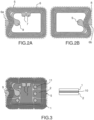
- FIG 2A represents a low-cost flexible plastic support type substrate 6 comprising on a first face 6a an antenna 5 (electrically conductive zone).
- the low cost carrier can be made of polyethylene terephthalate or PET, or polyvinyl chloride or PVC.
- the antenna 5 in this example has several turns of conductive material produced by etching or by an additive process (process where the surface of the desired pattern is activated to allow the growth of the conductor in a second step or the direct transfer of the conductor, by screen printing or transfer, for example).
- the first face 6a comprising the antenna 5 comprises two connection pads 7 which will be used to connect a chip 12 to provide a contactless function. The coupling between the electronic module and an antenna buried in the card will be done in this case by inductive coupling ( figure 5B ).
- FIG 2B represents a second antenna 8 deposited on the face 6b opposite the first face 6a of the substrate 6.
- the second antenna 8 is itself composed of several turns in this example.
- the two antennas 5, 8 double-sided antenna
- the two faces of the substrate are electrically connected by crimping 9 between jaws with force and ultrasound, known by the English expression “crimp”.
- the technology for making antennas can be the large-width engraving (a few tens of cm to several meters) of a two-layer aluminum complex on a PET dielectric.
- the two conductive layers will then be interconnected by "crimp".
- antennas It is possible to use copper or silver ink as conductive materials.
- the realization of the antennas will be done, for example, by additive growth of the conductive material according to the model (pattern) chosen or any other available technology.
- a layer of adhesive 10 is deposited on the low-cost substrate in order to allow it to be fixed on the grid.
- the assembly formed by the “adhesive-coated” support is then perforated with several orifices 11 or solder wells which will be used to connect the chip to the ISO pads of the gate, providing a contact function.
- the perforation step can be carried out before or after the deposition of the adhesive layer.
- the adhesive layer When the adhesive layer is deposited after perforation of the substrate, the adhesive layer will be pre-perforated.
- the position of the orifices is chosen according to the position of the contacts arranged on the external face of the grid.
- the number of orifices 11 is five for the contact function and the number of connection pads (without contact) 7 is two for the contactless function.
- the number of connection pads is chosen according to the application.
- the "adhesive" and perforated support is then glued to the hidden face 1b of the grid, the face which does not include the finish for the ISO connection.
- the adhesive layer 10 optionally multi-layered, with a resistant core, makes it possible in particular to electrically insulate the metal (ISO layer) from the antenna in the case of a double-sided antenna.
- the etching varnish may have been kept at least for this face in order to ensure its electrical insulation.
- the holes 11 reveal the wiring areas to form solder wells for the electrical connection of the chip 12.
- FIG 4 illustrates an example of several positions of the grid on a support in continuous format of the S35 type, Super 35mm format, known from skilled in the art, on which we will come to transfer a flexible film with its conductors, pierced and inexpensive according to the method described above.
- the next step, figure 5A consists in bonding an integrated circuit or chip 12 on the flexible substrate or at the level of the flexible substrate according to principles known to those skilled in the art.
- the chip 12 could be positioned at the level of an opening 15 (shown in dotted lines in figure 5B ) in the plastic support in order to gain thickness.
- the chip 12 is then connected to the connection pads 7 corresponding to the ends of the antenna in order to ensure the function without contact and via the solder wells 11 with the contact pads 12p of the chip in order to ensure the function with contact.
- An encapsulation 13 and protection resin is deposited, in order to encompass the chip and the connections.
- FIG. 5B shows in section the positioning of an electronic module manufactured by the method of the invention above a cavity of a card 21 comprising an antenna 22 (electric circuit) placed on a support 23 in order to provide a contactless function.
- the geometry and the dimensions of the cavity 24 are chosen for example according to the dimension of the electronic module.
- the support of the electronic module has a certain thickness, for example 350-400 ⁇ m, allowing the presence of two electrically conductive zones 31 (metallic material) replacing the antenna 5 in the form of turns of the electronic module.
- the coupling between the electronic module and the antenna buried in a card is then done by capacitive coupling.
- the contacts in the example given verify ISO standards, but could also be other contacts suitable for other applications.
- the antenna is replaced by two connection pads adapted to be connected to the antenna located in a card body.
- Different technologies can be used, for example, conventional technologies with anisotropic conductive embedding adhesive film or ACF, or with conductive bump or bump, or even by using a conductive glue, or a solder, between the metal surfaces 31 and the terminals of the core antenna in the card body.
- the steps described are carried out for the manufacture of modules for dual or hybrid cards comprising a chip and used for banking transactions.
- the method according to the invention and the module obtained can also be used in the field of identity, for passports for example, or in any other field using such portable objects.
- the electronic module obtained by the invention has a low manufacturing cost.
- the product can be flexibly adapted to be compatible with all known dual interface board manufacturing technologies.
Landscapes
- Engineering & Computer Science (AREA)
- Microelectronics & Electronic Packaging (AREA)
- Computer Hardware Design (AREA)
- Physics & Mathematics (AREA)
- General Physics & Mathematics (AREA)
- Theoretical Computer Science (AREA)
- Computer Networks & Wireless Communication (AREA)
- Credit Cards Or The Like (AREA)
- Printing Elements For Providing Electric Connections Between Printed Circuits (AREA)
Claims (13)
- - Verfahren zur Herstellung eines oder mehrerer elektronischer Module (20), dadurch gekennzeichnet, dass es mindestens die folgenden Schritte umfasst:Die Benutzung:Eines flexiblen Substrats (6) mit mehreren durchgehenden Anschlussöffnungen (11), einer ersten Seite (6a) mit mindestens einem elektrisch leitfähigen Bereich (5), an dessen Enden sich eine oder mehrere Anschlussflächen (7) befinden, und einer zweiten Seite (6b), undEines elektrisch leitfähigen Trägers (1), der eine erste Seite (1a) mit einem oder mehreren Anschlussbereichen (3) und eine zweite Seite (1b) umfasst,Das Zusammenfügen der zweiten Seite (6b) des flexiblen Substrats (6) und der zweiten Seite (1b) des elektrisch leitfähigen Trägers (1) mittels einer Klebeschicht,Das Positionieren eines integrierten Schaltkreises (12) auf oder an der ersten Seite (6a) des Substrats (6),Das Anschließen eines oder mehrerer Kontakte (12p) des integrierten Schaltkreises (12) an dem oder den Anschlussbereich(en) (3) über die Anschlussöffnungen (11), und an den Anschlussflächen (7),Das Auftragen einer Schutzschicht (13) auf den integrierten Schaltkreis.
- - Herstellungsverfahren nach Anspruch 1, dadurch gekennzeichnet, dass man das flexible Substrat und den elektrisch leitenden Träger zusammenfügt, bevor man die aus dem Substrat und der Klebeschicht gebildete Einheit perforiert.
- - Verfahren nach einem der Ansprüche 1 oder 2, dadurch gekennzeichnet, dass der elektrisch leitfähige Bereich (5) aus mehreren Windungen besteht, die eine Antenne bilden.
- - Verfahren nach Anspruch 3, dadurch gekennzeichnet, dass die Windungen aus Aluminium bestehen.
- - Verfahren nach Anspruch 3, dadurch gekennzeichnet, dass die Windungen aus Kupfer bestehen.
- - Verfahren nach Anspruch 3, dadurch gekennzeichnet, dass die Windungen aus gedrucktem, elektrisch leitfähigem Material bestehen.
- - Verfahren nach einem der Ansprüche 1 oder 2, dadurch gekennzeichnet, dass der elektrisch leitfähige Bereich (5) aus mindestens zwei Bereichen aus leitfähigem Material (31) gebildet wird, die um den integrierten Schaltkreis herum angeordnet sind.
- - Verfahren nach einem der vorhergehenden Ansprüche, dadurch gekennzeichnet, dass ein Substrat aus Polyethylenterephthalat (PET) oder Polyvinylchlorid (PVC) verwendet wird.
- - Elektronisches Modul, dadurch gekennzeichnet, dass es mindestens die folgenden Elemente umfasst:• Ein flexibles Substrat (6) mit einer ersten Seite (6a) mit mindestens einem elektrisch leitfähigen Bereich (5), an dessen Enden sich eine oder mehrere Anschlussflächen (7) befinden, und einer zweiten Seite (6b), wobei es mehrere durchgehende Anschlussöffnungen (11) umfasst,• Einen elektrisch leitfähigen Träger (1), der eine erste Seite (1a) mit einem oder mehreren Anschlussbereichen (3) und eine zweite Seite (1b) umfasst,• Das flexible Substrat (6) wird über die zweite Seite (6b) mittels einer Klebeschicht an der zweiten Seite (1b) des elektrisch leitfähigen Trägers (1) befestigt,• Einen integrierten Schaltkreis (12), der auf oder an der ersten Seite (6a) des Substrats (6) angeordnet ist, wobei der integrierte Schaltkreis (12) über einen oder mehrere Kontakte (12p) mit dem mindestens einen elektrisch leitfähigen Bereich (5) über die Anschlussöffnungen (11) verbunden ist,• Eine Schutzschicht (13) zumindest auf dem integrierten Schaltkreis.
- - Elektronisches Modul nach Anspruch 9, dadurch gekennzeichnet, dass das Substrat aus Polyethylenterephthalat (PET) oder aus Polyvinylchlorid (PVC) besteht.
- - Elektronisches Modul nach einem der Ansprüche 9 oder 10, dadurch gekennzeichnet, dass der elektrisch leitfähige Bereich (5) eine Antenne ist, die durch mindestens eine Windung gebildet wird, die auf mindestens einer Seite des Substrats angebracht ist.
- - Elektronisches Modul nach einem der Ansprüche 9 oder 10, dadurch gekennzeichnet, dass der elektrisch leitfähige Bereich (5) aus mindestens zwei Bereichen aus leitfähigem Material (31) gebildet wird, die um den integrierten Schaltkreis herum angeordnet sind.
- - Karte mit einem elektronischen Modul nach einem der Ansprüche 9 bis 12, das in einem Hohlraum (13) der Karte angeordnet ist, und einer Antenne, die im Körper der Karte angebracht ist.
Applications Claiming Priority (2)
| Application Number | Priority Date | Filing Date | Title |
|---|---|---|---|
| FR1858425A FR3086098B1 (fr) | 2018-09-18 | 2018-09-18 | Procede de fabrication d'un module electronique pour objet portatif |
| PCT/EP2019/074069 WO2020058036A1 (fr) | 2018-09-18 | 2019-09-10 | Procede de fabrication d'un module electronique pour objet portatif |
Publications (2)
| Publication Number | Publication Date |
|---|---|
| EP3853773A1 EP3853773A1 (de) | 2021-07-28 |
| EP3853773B1 true EP3853773B1 (de) | 2023-07-26 |
Family
ID=65201497
Family Applications (1)
| Application Number | Title | Priority Date | Filing Date |
|---|---|---|---|
| EP19763008.0A Active EP3853773B1 (de) | 2018-09-18 | 2019-09-10 | Verfahren zur herstellung eines elektronischen moduls für ein tragbares objekt |
Country Status (5)
| Country | Link |
|---|---|
| EP (1) | EP3853773B1 (de) |
| KR (1) | KR20210060476A (de) |
| CN (1) | CN112703510B (de) |
| FR (1) | FR3086098B1 (de) |
| WO (1) | WO2020058036A1 (de) |
Families Citing this family (1)
| Publication number | Priority date | Publication date | Assignee | Title |
|---|---|---|---|---|
| EP4490655B1 (de) * | 2023-03-22 | 2025-12-03 | Smartflex Technology Pte Ltd | Herstellungsartikel in bezug auf ic-module und chipkarten |
Family Cites Families (14)
| Publication number | Priority date | Publication date | Assignee | Title |
|---|---|---|---|---|
| FR2880160B1 (fr) * | 2004-12-28 | 2007-03-30 | K Sa As | Module electronique double face pour carte a puce hybride |
| JP4952266B2 (ja) * | 2007-01-18 | 2012-06-13 | 大日本印刷株式会社 | デュアルインターフェースicカードとその製造方法、接触・非接触兼用icモジュール |
| WO2009078810A1 (en) * | 2007-12-19 | 2009-06-25 | Linda Seah | Contact-less and dual interface inlays and methods for producing the same |
| CN101350073B (zh) * | 2008-08-20 | 2010-06-23 | 北京握奇数据系统有限公司 | 双界面智能卡的生产方法、双界面智能卡及其天线层 |
| CN102663480B (zh) * | 2012-03-24 | 2016-05-25 | 上海仪电智能电子有限公司 | 一种双界面智能卡 |
| FR2992761B1 (fr) * | 2012-07-02 | 2015-05-29 | Inside Secure | Procede de fabrication d'un microcircuit sans contact |
| FR2996944B1 (fr) * | 2012-10-15 | 2018-05-04 | Smart Packaging Solutions Sps | Module electronique simplifie pour carte a puce a double interface de communication |
| EP2825001A1 (de) * | 2013-07-10 | 2015-01-14 | Gemalto SA | Elektronisches Modul mit klebende dielektrische Beschichtung, und sein Herstellungsverfahren |
| US10091883B2 (en) * | 2013-07-10 | 2018-10-02 | Gemalto Sa | Dielectric filmless electronic module and method for manufacturing same |
| EP2871595A1 (de) * | 2013-11-12 | 2015-05-13 | Gemalto SA | Chipkarte, die ein elektronisches Modul umfasst, das elektrisch an einen Stromkreis angeschlossen ist |
| WO2015157659A1 (en) * | 2014-04-10 | 2015-10-15 | American Banknote Corporation | Integrated circuit module for a dual-interface smart card |
| FR3021145B1 (fr) * | 2014-05-14 | 2018-08-31 | Linxens Holding | Procede de fabrication d'un circuit pour module de carte a puce et circuit pour module de carte a puce |
| EP3159831B1 (de) * | 2015-10-21 | 2018-10-03 | Nxp B.V. | Dual-interface ic-karte |
| FR3047101B1 (fr) * | 2016-01-26 | 2022-04-01 | Linxens Holding | Procede de fabrication d’un module de carte a puce et d’une carte a puce |
-
2018
- 2018-09-18 FR FR1858425A patent/FR3086098B1/fr not_active Expired - Fee Related
-
2019
- 2019-09-10 EP EP19763008.0A patent/EP3853773B1/de active Active
- 2019-09-10 WO PCT/EP2019/074069 patent/WO2020058036A1/fr not_active Ceased
- 2019-09-10 CN CN201980060756.6A patent/CN112703510B/zh not_active Expired - Fee Related
- 2019-09-10 KR KR1020217008059A patent/KR20210060476A/ko not_active Ceased
Also Published As
| Publication number | Publication date |
|---|---|
| KR20210060476A (ko) | 2021-05-26 |
| FR3086098A1 (fr) | 2020-03-20 |
| FR3086098B1 (fr) | 2020-12-04 |
| CN112703510B (zh) | 2024-02-20 |
| WO2020058036A1 (fr) | 2020-03-26 |
| CN112703510A (zh) | 2021-04-23 |
| EP3853773A1 (de) | 2021-07-28 |
Similar Documents
| Publication | Publication Date | Title |
|---|---|---|
| EP0671705B1 (de) | Herstellungsverfahren einer Kombi-Karte | |
| EP3567527B1 (de) | Herstellungsverfahren eines schaltkreises für chipkartenmodul, und schaltkreis für chipkartenmodul | |
| EP3877909B1 (de) | Elektronisches modul für chipkarte | |
| EP3574451B1 (de) | Rfid-vorrichtung und verfahren zur herstellung davon | |
| EP3956815A1 (de) | Biometrisches sensormodul für eine chipkarte und verfahren zur herstellung eines solchen moduls | |
| FR3003723A1 (fr) | Procede de fabrication d'un circuit imprime flexible, circuit imprime flexible obtenu par ce procede et module de carte a puce comportant un tel circuit imprime flexible | |
| WO2014191428A1 (fr) | Procédé de fabrication d'un circuit imprimé, circuit imprimé obtenu par ce procédé et module électronique comportant un tel circuit imprimé | |
| EP3092604B1 (de) | Elektronisches modul, sein herstellungsverfahren und dieses modul umfassende elektronische vorrichtung | |
| WO2020058036A1 (fr) | Procede de fabrication d'un module electronique pour objet portatif | |
| EP2915104B1 (de) | Verfahren zur herstellung einer anschlussvorrichtung für das modul einer smart card, durch das verfahren erhaltene anschlussvorrichtung und modul mit smart card anschlussvorrichtung | |
| FR3083892A1 (fr) | Carte a puce a double interface de communication et son procede de fabrication | |
| EP3853775B1 (de) | Verfahren zur herstellung eines kartenmoduls und hergestelltes modul | |
| EP2866173A1 (de) | Verfahren zur Erzeugung eines elektrischen Schaltkreises, und mit diesem Verfahren erzeugter Schaltkreis | |
| FR2795202A1 (fr) | Carte et procede de fabrication de cartes ayant une interface de communication a contact et sans contact | |
| EP3020068B1 (de) | Elektronisches modul und verfahren zur herstellung davon | |
| EP4193423B1 (de) | Elektronisches modul für eine karte mit mindestens einer antenne und herstellungsverfahren dafür | |
| FR3005391A1 (fr) | Procede de fabrication d'un circuit flexible pour module de carte a puce, circuit flexible de carte a puce otenu par ce procede et module de carte a puce comportant un tel circuit flexible | |
| EP1190379A1 (de) | Verfahren zur herstellung einer chip-karte mit kontakten mit kostengünstigem dielektrikum | |
| WO2017153353A1 (fr) | Procede de fabrication de module a puce de circuit integre et dispositif comprenant un tel module |
Legal Events
| Date | Code | Title | Description |
|---|---|---|---|
| STAA | Information on the status of an ep patent application or granted ep patent |
Free format text: STATUS: UNKNOWN |
|
| STAA | Information on the status of an ep patent application or granted ep patent |
Free format text: STATUS: THE INTERNATIONAL PUBLICATION HAS BEEN MADE |
|
| PUAI | Public reference made under article 153(3) epc to a published international application that has entered the european phase |
Free format text: ORIGINAL CODE: 0009012 |
|
| STAA | Information on the status of an ep patent application or granted ep patent |
Free format text: STATUS: REQUEST FOR EXAMINATION WAS MADE |
|
| 17P | Request for examination filed |
Effective date: 20210225 |
|
| AK | Designated contracting states |
Kind code of ref document: A1 Designated state(s): AL AT BE BG CH CY CZ DE DK EE ES FI FR GB GR HR HU IE IS IT LI LT LU LV MC MK MT NL NO PL PT RO RS SE SI SK SM TR |
|
| DAV | Request for validation of the european patent (deleted) | ||
| DAX | Request for extension of the european patent (deleted) | ||
| GRAP | Despatch of communication of intention to grant a patent |
Free format text: ORIGINAL CODE: EPIDOSNIGR1 |
|
| STAA | Information on the status of an ep patent application or granted ep patent |
Free format text: STATUS: GRANT OF PATENT IS INTENDED |
|
| INTG | Intention to grant announced |
Effective date: 20230214 |
|
| GRAS | Grant fee paid |
Free format text: ORIGINAL CODE: EPIDOSNIGR3 |
|
| GRAA | (expected) grant |
Free format text: ORIGINAL CODE: 0009210 |
|
| STAA | Information on the status of an ep patent application or granted ep patent |
Free format text: STATUS: THE PATENT HAS BEEN GRANTED |
|
| AK | Designated contracting states |
Kind code of ref document: B1 Designated state(s): AL AT BE BG CH CY CZ DE DK EE ES FI FR GB GR HR HU IE IS IT LI LT LU LV MC MK MT NL NO PL PT RO RS SE SI SK SM TR |
|
| REG | Reference to a national code |
Ref country code: CH Ref legal event code: EP |
|
| REG | Reference to a national code |
Ref country code: DE Ref legal event code: R096 Ref document number: 602019033602 Country of ref document: DE |
|
| REG | Reference to a national code |
Ref country code: IE Ref legal event code: FG4D Free format text: LANGUAGE OF EP DOCUMENT: FRENCH |
|
| REG | Reference to a national code |
Ref country code: LT Ref legal event code: MG9D |
|
| REG | Reference to a national code |
Ref country code: NL Ref legal event code: MP Effective date: 20230726 |
|
| REG | Reference to a national code |
Ref country code: AT Ref legal event code: MK05 Ref document number: 1592789 Country of ref document: AT Kind code of ref document: T Effective date: 20230726 |
|
| PG25 | Lapsed in a contracting state [announced via postgrant information from national office to epo] |
Ref country code: NL Free format text: LAPSE BECAUSE OF FAILURE TO SUBMIT A TRANSLATION OF THE DESCRIPTION OR TO PAY THE FEE WITHIN THE PRESCRIBED TIME-LIMIT Effective date: 20230726 |
|
| PG25 | Lapsed in a contracting state [announced via postgrant information from national office to epo] |
Ref country code: GR Free format text: LAPSE BECAUSE OF FAILURE TO SUBMIT A TRANSLATION OF THE DESCRIPTION OR TO PAY THE FEE WITHIN THE PRESCRIBED TIME-LIMIT Effective date: 20231027 |
|
| PGFP | Annual fee paid to national office [announced via postgrant information from national office to epo] |
Ref country code: GB Payment date: 20231121 Year of fee payment: 5 |
|
| PG25 | Lapsed in a contracting state [announced via postgrant information from national office to epo] |
Ref country code: IS Free format text: LAPSE BECAUSE OF FAILURE TO SUBMIT A TRANSLATION OF THE DESCRIPTION OR TO PAY THE FEE WITHIN THE PRESCRIBED TIME-LIMIT Effective date: 20231126 |
|
| PG25 | Lapsed in a contracting state [announced via postgrant information from national office to epo] |
Ref country code: SE Free format text: LAPSE BECAUSE OF FAILURE TO SUBMIT A TRANSLATION OF THE DESCRIPTION OR TO PAY THE FEE WITHIN THE PRESCRIBED TIME-LIMIT Effective date: 20230726 Ref country code: RS Free format text: LAPSE BECAUSE OF FAILURE TO SUBMIT A TRANSLATION OF THE DESCRIPTION OR TO PAY THE FEE WITHIN THE PRESCRIBED TIME-LIMIT Effective date: 20230726 Ref country code: PT Free format text: LAPSE BECAUSE OF FAILURE TO SUBMIT A TRANSLATION OF THE DESCRIPTION OR TO PAY THE FEE WITHIN THE PRESCRIBED TIME-LIMIT Effective date: 20231127 Ref country code: NO Free format text: LAPSE BECAUSE OF FAILURE TO SUBMIT A TRANSLATION OF THE DESCRIPTION OR TO PAY THE FEE WITHIN THE PRESCRIBED TIME-LIMIT Effective date: 20231026 Ref country code: LV Free format text: LAPSE BECAUSE OF FAILURE TO SUBMIT A TRANSLATION OF THE DESCRIPTION OR TO PAY THE FEE WITHIN THE PRESCRIBED TIME-LIMIT Effective date: 20230726 Ref country code: LT Free format text: LAPSE BECAUSE OF FAILURE TO SUBMIT A TRANSLATION OF THE DESCRIPTION OR TO PAY THE FEE WITHIN THE PRESCRIBED TIME-LIMIT Effective date: 20230726 Ref country code: IS Free format text: LAPSE BECAUSE OF FAILURE TO SUBMIT A TRANSLATION OF THE DESCRIPTION OR TO PAY THE FEE WITHIN THE PRESCRIBED TIME-LIMIT Effective date: 20231126 Ref country code: HR Free format text: LAPSE BECAUSE OF FAILURE TO SUBMIT A TRANSLATION OF THE DESCRIPTION OR TO PAY THE FEE WITHIN THE PRESCRIBED TIME-LIMIT Effective date: 20230726 Ref country code: GR Free format text: LAPSE BECAUSE OF FAILURE TO SUBMIT A TRANSLATION OF THE DESCRIPTION OR TO PAY THE FEE WITHIN THE PRESCRIBED TIME-LIMIT Effective date: 20231027 Ref country code: FI Free format text: LAPSE BECAUSE OF FAILURE TO SUBMIT A TRANSLATION OF THE DESCRIPTION OR TO PAY THE FEE WITHIN THE PRESCRIBED TIME-LIMIT Effective date: 20230726 Ref country code: AT Free format text: LAPSE BECAUSE OF FAILURE TO SUBMIT A TRANSLATION OF THE DESCRIPTION OR TO PAY THE FEE WITHIN THE PRESCRIBED TIME-LIMIT Effective date: 20230726 |
|
| PGFP | Annual fee paid to national office [announced via postgrant information from national office to epo] |
Ref country code: FR Payment date: 20231121 Year of fee payment: 5 Ref country code: DE Payment date: 20231120 Year of fee payment: 5 |
|
| PG25 | Lapsed in a contracting state [announced via postgrant information from national office to epo] |
Ref country code: PL Free format text: LAPSE BECAUSE OF FAILURE TO SUBMIT A TRANSLATION OF THE DESCRIPTION OR TO PAY THE FEE WITHIN THE PRESCRIBED TIME-LIMIT Effective date: 20230726 |
|
| PG25 | Lapsed in a contracting state [announced via postgrant information from national office to epo] |
Ref country code: ES Free format text: LAPSE BECAUSE OF FAILURE TO SUBMIT A TRANSLATION OF THE DESCRIPTION OR TO PAY THE FEE WITHIN THE PRESCRIBED TIME-LIMIT Effective date: 20230726 |
|
| REG | Reference to a national code |
Ref country code: DE Ref legal event code: R097 Ref document number: 602019033602 Country of ref document: DE |
|
| PG25 | Lapsed in a contracting state [announced via postgrant information from national office to epo] |
Ref country code: SM Free format text: LAPSE BECAUSE OF FAILURE TO SUBMIT A TRANSLATION OF THE DESCRIPTION OR TO PAY THE FEE WITHIN THE PRESCRIBED TIME-LIMIT Effective date: 20230726 Ref country code: RO Free format text: LAPSE BECAUSE OF FAILURE TO SUBMIT A TRANSLATION OF THE DESCRIPTION OR TO PAY THE FEE WITHIN THE PRESCRIBED TIME-LIMIT Effective date: 20230726 Ref country code: ES Free format text: LAPSE BECAUSE OF FAILURE TO SUBMIT A TRANSLATION OF THE DESCRIPTION OR TO PAY THE FEE WITHIN THE PRESCRIBED TIME-LIMIT Effective date: 20230726 Ref country code: EE Free format text: LAPSE BECAUSE OF FAILURE TO SUBMIT A TRANSLATION OF THE DESCRIPTION OR TO PAY THE FEE WITHIN THE PRESCRIBED TIME-LIMIT Effective date: 20230726 Ref country code: DK Free format text: LAPSE BECAUSE OF FAILURE TO SUBMIT A TRANSLATION OF THE DESCRIPTION OR TO PAY THE FEE WITHIN THE PRESCRIBED TIME-LIMIT Effective date: 20230726 Ref country code: CZ Free format text: LAPSE BECAUSE OF FAILURE TO SUBMIT A TRANSLATION OF THE DESCRIPTION OR TO PAY THE FEE WITHIN THE PRESCRIBED TIME-LIMIT Effective date: 20230726 Ref country code: SK Free format text: LAPSE BECAUSE OF FAILURE TO SUBMIT A TRANSLATION OF THE DESCRIPTION OR TO PAY THE FEE WITHIN THE PRESCRIBED TIME-LIMIT Effective date: 20230726 |
|
| REG | Reference to a national code |
Ref country code: CH Ref legal event code: PL |
|
| PG25 | Lapsed in a contracting state [announced via postgrant information from national office to epo] |
Ref country code: LU Free format text: LAPSE BECAUSE OF NON-PAYMENT OF DUE FEES Effective date: 20230910 |
|
| REG | Reference to a national code |
Ref country code: BE Ref legal event code: MM Effective date: 20230930 |
|
| PG25 | Lapsed in a contracting state [announced via postgrant information from national office to epo] |
Ref country code: LU Free format text: LAPSE BECAUSE OF NON-PAYMENT OF DUE FEES Effective date: 20230910 Ref country code: IT Free format text: LAPSE BECAUSE OF FAILURE TO SUBMIT A TRANSLATION OF THE DESCRIPTION OR TO PAY THE FEE WITHIN THE PRESCRIBED TIME-LIMIT Effective date: 20230726 Ref country code: MC Free format text: LAPSE BECAUSE OF FAILURE TO SUBMIT A TRANSLATION OF THE DESCRIPTION OR TO PAY THE FEE WITHIN THE PRESCRIBED TIME-LIMIT Effective date: 20230726 |
|
| PLBE | No opposition filed within time limit |
Free format text: ORIGINAL CODE: 0009261 |
|
| STAA | Information on the status of an ep patent application or granted ep patent |
Free format text: STATUS: NO OPPOSITION FILED WITHIN TIME LIMIT |
|
| 26N | No opposition filed |
Effective date: 20240429 |
|
| REG | Reference to a national code |
Ref country code: IE Ref legal event code: MM4A |
|
| PG25 | Lapsed in a contracting state [announced via postgrant information from national office to epo] |
Ref country code: IE Free format text: LAPSE BECAUSE OF NON-PAYMENT OF DUE FEES Effective date: 20230910 |
|
| PG25 | Lapsed in a contracting state [announced via postgrant information from national office to epo] |
Ref country code: CH Free format text: LAPSE BECAUSE OF NON-PAYMENT OF DUE FEES Effective date: 20230930 |
|
| PG25 | Lapsed in a contracting state [announced via postgrant information from national office to epo] |
Ref country code: IE Free format text: LAPSE BECAUSE OF NON-PAYMENT OF DUE FEES Effective date: 20230910 Ref country code: CH Free format text: LAPSE BECAUSE OF NON-PAYMENT OF DUE FEES Effective date: 20230930 Ref country code: SI Free format text: LAPSE BECAUSE OF FAILURE TO SUBMIT A TRANSLATION OF THE DESCRIPTION OR TO PAY THE FEE WITHIN THE PRESCRIBED TIME-LIMIT Effective date: 20230726 |
|
| PG25 | Lapsed in a contracting state [announced via postgrant information from national office to epo] |
Ref country code: BE Free format text: LAPSE BECAUSE OF NON-PAYMENT OF DUE FEES Effective date: 20230930 |
|
| PG25 | Lapsed in a contracting state [announced via postgrant information from national office to epo] |
Ref country code: BG Free format text: LAPSE BECAUSE OF FAILURE TO SUBMIT A TRANSLATION OF THE DESCRIPTION OR TO PAY THE FEE WITHIN THE PRESCRIBED TIME-LIMIT Effective date: 20230726 |
|
| PG25 | Lapsed in a contracting state [announced via postgrant information from national office to epo] |
Ref country code: BG Free format text: LAPSE BECAUSE OF FAILURE TO SUBMIT A TRANSLATION OF THE DESCRIPTION OR TO PAY THE FEE WITHIN THE PRESCRIBED TIME-LIMIT Effective date: 20230726 |
|
| REG | Reference to a national code |
Ref country code: DE Ref legal event code: R119 Ref document number: 602019033602 Country of ref document: DE |
|
| GBPC | Gb: european patent ceased through non-payment of renewal fee |
Effective date: 20240910 |
|
| PG25 | Lapsed in a contracting state [announced via postgrant information from national office to epo] |
Ref country code: DE Free format text: LAPSE BECAUSE OF NON-PAYMENT OF DUE FEES Effective date: 20250401 |
|
| PG25 | Lapsed in a contracting state [announced via postgrant information from national office to epo] |
Ref country code: GB Free format text: LAPSE BECAUSE OF NON-PAYMENT OF DUE FEES Effective date: 20240910 |
|
| PG25 | Lapsed in a contracting state [announced via postgrant information from national office to epo] |
Ref country code: FR Free format text: LAPSE BECAUSE OF NON-PAYMENT OF DUE FEES Effective date: 20240930 |
|
| PG25 | Lapsed in a contracting state [announced via postgrant information from national office to epo] |
Ref country code: CY Free format text: LAPSE BECAUSE OF FAILURE TO SUBMIT A TRANSLATION OF THE DESCRIPTION OR TO PAY THE FEE WITHIN THE PRESCRIBED TIME-LIMIT; INVALID AB INITIO Effective date: 20190910 |
|
| PG25 | Lapsed in a contracting state [announced via postgrant information from national office to epo] |
Ref country code: HU Free format text: LAPSE BECAUSE OF FAILURE TO SUBMIT A TRANSLATION OF THE DESCRIPTION OR TO PAY THE FEE WITHIN THE PRESCRIBED TIME-LIMIT; INVALID AB INITIO Effective date: 20190910 |
|
| PG25 | Lapsed in a contracting state [announced via postgrant information from national office to epo] |
Ref country code: TR Free format text: LAPSE BECAUSE OF FAILURE TO SUBMIT A TRANSLATION OF THE DESCRIPTION OR TO PAY THE FEE WITHIN THE PRESCRIBED TIME-LIMIT Effective date: 20230726 |