EP3877909B1 - Elektronisches modul für chipkarte - Google Patents
Elektronisches modul für chipkarte Download PDFInfo
- Publication number
- EP3877909B1 EP3877909B1 EP19780270.5A EP19780270A EP3877909B1 EP 3877909 B1 EP3877909 B1 EP 3877909B1 EP 19780270 A EP19780270 A EP 19780270A EP 3877909 B1 EP3877909 B1 EP 3877909B1
- Authority
- EP
- European Patent Office
- Prior art keywords
- substrate
- electrically conductive
- film
- areas
- integrated circuit
- Prior art date
- Legal status (The legal status is an assumption and is not a legal conclusion. Google has not performed a legal analysis and makes no representation as to the accuracy of the status listed.)
- Active
Links
Images


Classifications
-
- G—PHYSICS
- G06—COMPUTING OR CALCULATING; COUNTING
- G06K—GRAPHICAL DATA READING; PRESENTATION OF DATA; RECORD CARRIERS; HANDLING RECORD CARRIERS
- G06K19/00—Record carriers for use with machines and with at least a part designed to carry digital markings
- G06K19/06—Record carriers for use with machines and with at least a part designed to carry digital markings characterised by the kind of the digital marking, e.g. shape, nature, code
- G06K19/067—Record carriers with conductive marks, printed circuits or semiconductor circuit elements, e.g. credit or identity cards also with resonating or responding marks without active components
- G06K19/07—Record carriers with conductive marks, printed circuits or semiconductor circuit elements, e.g. credit or identity cards also with resonating or responding marks without active components with integrated circuit chips
- G06K19/077—Constructional details, e.g. mounting of circuits in the carrier
- G06K19/07745—Mounting details of integrated circuit chips
-
- G—PHYSICS
- G06—COMPUTING OR CALCULATING; COUNTING
- G06K—GRAPHICAL DATA READING; PRESENTATION OF DATA; RECORD CARRIERS; HANDLING RECORD CARRIERS
- G06K19/00—Record carriers for use with machines and with at least a part designed to carry digital markings
- G06K19/06—Record carriers for use with machines and with at least a part designed to carry digital markings characterised by the kind of the digital marking, e.g. shape, nature, code
- G06K19/067—Record carriers with conductive marks, printed circuits or semiconductor circuit elements, e.g. credit or identity cards also with resonating or responding marks without active components
- G06K19/07—Record carriers with conductive marks, printed circuits or semiconductor circuit elements, e.g. credit or identity cards also with resonating or responding marks without active components with integrated circuit chips
- G06K19/077—Constructional details, e.g. mounting of circuits in the carrier
- G06K19/07749—Constructional details, e.g. mounting of circuits in the carrier the record carrier being capable of non-contact communication, e.g. constructional details of the antenna of a non-contact smart card
- G06K19/0775—Constructional details, e.g. mounting of circuits in the carrier the record carrier being capable of non-contact communication, e.g. constructional details of the antenna of a non-contact smart card arrangements for connecting the integrated circuit to the antenna
-
- G—PHYSICS
- G06—COMPUTING OR CALCULATING; COUNTING
- G06K—GRAPHICAL DATA READING; PRESENTATION OF DATA; RECORD CARRIERS; HANDLING RECORD CARRIERS
- G06K19/00—Record carriers for use with machines and with at least a part designed to carry digital markings
- G06K19/06—Record carriers for use with machines and with at least a part designed to carry digital markings characterised by the kind of the digital marking, e.g. shape, nature, code
- G06K19/067—Record carriers with conductive marks, printed circuits or semiconductor circuit elements, e.g. credit or identity cards also with resonating or responding marks without active components
- G06K19/07—Record carriers with conductive marks, printed circuits or semiconductor circuit elements, e.g. credit or identity cards also with resonating or responding marks without active components with integrated circuit chips
- G06K19/077—Constructional details, e.g. mounting of circuits in the carrier
- G06K19/07749—Constructional details, e.g. mounting of circuits in the carrier the record carrier being capable of non-contact communication, e.g. constructional details of the antenna of a non-contact smart card
- G06K19/0775—Constructional details, e.g. mounting of circuits in the carrier the record carrier being capable of non-contact communication, e.g. constructional details of the antenna of a non-contact smart card arrangements for connecting the integrated circuit to the antenna
- G06K19/07754—Constructional details, e.g. mounting of circuits in the carrier the record carrier being capable of non-contact communication, e.g. constructional details of the antenna of a non-contact smart card arrangements for connecting the integrated circuit to the antenna the connection being galvanic
-
- G—PHYSICS
- G06—COMPUTING OR CALCULATING; COUNTING
- G06K—GRAPHICAL DATA READING; PRESENTATION OF DATA; RECORD CARRIERS; HANDLING RECORD CARRIERS
- G06K19/00—Record carriers for use with machines and with at least a part designed to carry digital markings
- G06K19/06—Record carriers for use with machines and with at least a part designed to carry digital markings characterised by the kind of the digital marking, e.g. shape, nature, code
- G06K19/067—Record carriers with conductive marks, printed circuits or semiconductor circuit elements, e.g. credit or identity cards also with resonating or responding marks without active components
- G06K19/07—Record carriers with conductive marks, printed circuits or semiconductor circuit elements, e.g. credit or identity cards also with resonating or responding marks without active components with integrated circuit chips
- G06K19/077—Constructional details, e.g. mounting of circuits in the carrier
- G06K19/07749—Constructional details, e.g. mounting of circuits in the carrier the record carrier being capable of non-contact communication, e.g. constructional details of the antenna of a non-contact smart card
- G06K19/07766—Constructional details, e.g. mounting of circuits in the carrier the record carrier being capable of non-contact communication, e.g. constructional details of the antenna of a non-contact smart card comprising at least a second communication arrangement in addition to a first non-contact communication arrangement
- G06K19/07769—Constructional details, e.g. mounting of circuits in the carrier the record carrier being capable of non-contact communication, e.g. constructional details of the antenna of a non-contact smart card comprising at least a second communication arrangement in addition to a first non-contact communication arrangement the further communication means being a galvanic interface, e.g. hybrid or mixed smart cards having a contact and a non-contact interface
-
- G—PHYSICS
- G06—COMPUTING OR CALCULATING; COUNTING
- G06K—GRAPHICAL DATA READING; PRESENTATION OF DATA; RECORD CARRIERS; HANDLING RECORD CARRIERS
- G06K19/00—Record carriers for use with machines and with at least a part designed to carry digital markings
- G06K19/06—Record carriers for use with machines and with at least a part designed to carry digital markings characterised by the kind of the digital marking, e.g. shape, nature, code
- G06K19/067—Record carriers with conductive marks, printed circuits or semiconductor circuit elements, e.g. credit or identity cards also with resonating or responding marks without active components
- G06K19/07—Record carriers with conductive marks, printed circuits or semiconductor circuit elements, e.g. credit or identity cards also with resonating or responding marks without active components with integrated circuit chips
- G06K19/077—Constructional details, e.g. mounting of circuits in the carrier
- G06K19/07749—Constructional details, e.g. mounting of circuits in the carrier the record carrier being capable of non-contact communication, e.g. constructional details of the antenna of a non-contact smart card
- G06K19/07773—Antenna details
- G06K19/07775—Antenna details the antenna being on-chip
Definitions
- the invention relates to an electronic module for a portable object having a dual function, with contact and without contact, for example a smart card.
- Electronic modules are generally produced on flexible printed circuits with one or two layers of etched and metallized copper.
- the pads of the integrated circuit chip are electrically connected to the contact plates of the connection housing by means of conductive wires.
- the electronic module also comprises an antenna or a pair of contact plates internal to the chip, arranged on the hidden face of the connection housing.
- the antenna is electrically connected to the chip via pads and by means of conductive wires (wire bonding) or by a direct connection technique using conductive bosses or "bumps".
- the type of substrate used is generally quite expensive.
- an antenna is integrated into the module and allows electromagnetic coupling with a “booster” antenna incorporated in the rigid support of the card.
- the patent application WO 2011/157693 discloses a multilayer printed circuit composed of a stack of several electrical layers and insulating layers.
- the object of the invention is to propose a new electronic module for a smart card and a new manufacturing method which makes it possible to offer flexibility in the design of the antenna and also to reduce manufacturing costs by combining a single-sided film comprising the contacts and a complex comprising at least one electrically conductive zone such as an antenna, while ensuring the usual functions with contact and/or without contact.
- a substrate comprising at least one electrically conductive zone consisting of turns forming an antenna and at least one contact pad located at at least one end of the antenna.
- At least one of said electrically conductive zones consists of at least one surface of conductive material.
- one or more orifices are made at the substrate level, the orifices corresponding to the orifices located in the film. in order to form solder wells between the integrated circuit and the contact areas.
- a substrate having one or more electrically conductive areas of aluminum is used to form the antenna or the conductive material surfaces.
- the pattern of the electrically conductive area or the conductive material surfaces can be made using an etching technique, an additive process by screen printing or transfer.
- the substrate comprises, for example, at least one of said electrically conductive zones in the form of turns comprising at one end a connection pad.
- It may also comprise at least one of said electrically conductive zones consisting of at least one surface of conductive material.
- the substrate may also include one or more perforations corresponding to the holes in the single-sided film in order to achieve the connection of the integrated circuit to the contact areas.
- the dielectric and/or substrate are selected from the following list: glass-epoxy, Polyethylene Naphthalate PEN, Polyethylene Terephthalate PET, or Polyvinyl Chloride PVC and the substrate carrying the antenna in PET or PVC.
- the figures represent a single module, knowing that the antennas will, in most cases, be manufactured on a large width strip (a few tens of cm to several meters), allowing a larger production.
- FIG. 1 illustrates a smart card 1 comprising at least one electronic module 2 obtained by implementing the method according to the invention.
- the electronic module 2 integrated in the smart card 1 has contacts 3 or contact zones at the surface of the front face of the card in order to allow its electrical connection with a card reader, not shown for reasons of simplification of drawings.
- FIG 2 illustrates the single-sided film 4 with contact via its upper face, the face which will be in contact with the reader.
- the single-sided film 4 supports the contacts 3 which are made on one face 4a and a dielectric 5 on the other face 4b. Openings 50 are made in the dielectric 5 to give access to all or part of the contacts.
- the position and dimensions of the contacts of the module are defined by the standard associated with the use of the card, for example, the ISO standard.
- the dielectric layer can also be a polyimide or PI layer.
- Materials such as PEN (Polyethylene Naphthalate), PET (Polyethylene terephthalate) or PVC (Polyvinyl chloride) can be used.
- PEN Polyethylene Naphthalate
- PET Polyethylene terephthalate
- PVC Polyvinyl chloride
- antenna 7 ( Figures 3A, 3B ) is done separately from the manufacture of the film comprising the contacts.
- the substrate 6 carrying the antenna will then be laminated onto the film carrying the contacts.
- a single substrate will be used
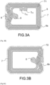
- FIGS 3A and 3B respectively illustrate a first face 6a and a second face 6b of a substrate 6 supporting one or more electrically conductive zones such as two antennas 71, 72 (constituting the two faces of an antenna).
- the antenna 71 comprises two pads 7p1, 7p2, for the connection.
- the Figures 3A and 3B illustrate an “antenna module” that can be produced on a flexible support in wide width as is known to those skilled in the art.
- the antenna is produced using, for example, an etching technique or an additive process, a process where the surface of the desired pattern is activated to allow the growth of the conductor or the direct transfer of the conductor, by screen printing or transfer, for example.
- the material used to make the antenna will be, for example, aluminum or any other electrically conductive metallic material with equivalent properties and which will be compatible with the adhesive material used to secure the contact film to the substrate carrying the antenna.
- the substrate carrying the antenna is a low-cost flexible support of the PET or PVC type or made from one of the aforementioned materials for the dielectric.
- the two antennas 71, 72 are connected by crimp 8 (electrical connection by crimping between jaws with force and ultrasound).
- the crimp zones can be in the form of zones circular. The area around the edge of the module can be cut out when cutting the module.
- FIG. 3C illustrates an alternative embodiment in which the antenna of the Figure 3A is replaced by at least one electrically conductive, metallic surface enabling communication for a contactless function of the portable object.
- the metallic pad may consist of two electrically conductive, metallic surfaces 75, 76, as illustrated in Figure 3C The two surfaces form two connection pads for a contactless function or allow capacitive coupling with a booster antenna integrated in the card body.
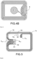
- FIGS. 4A And 4B illustrate a second variant embodiment which is not according to the invention in which the crimp zones 8 have a larger surface area, thus increasing the performance of the electrical connection.
- FIG 5 schematizes another variant embodiment, with a double-sided antenna 71, 72, one of the faces 72 of the antenna being illustrated by dotted lines.
- the interconnection of the two antennas is achieved by the use of a wire or "strap" 51 passing through a first opening 52 or via.
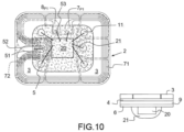
- the chip 20 ( figure 10 ) will be connected to one end of the antenna 71 located on a first face by means of a connection pad 7p1 and to a pad 8p1 of the antenna 72 located on the second face, through an orifice 53 or via.
- the vias 52, 53 may be made at the same time as the antenna is made, for example by laser scanning.
- a crimp (identical to that of the Figure 3A ) to connect the two antennas 71, 72 constituting the antenna.
- Two areas of the rear metal face are uncovered and cleaned by a combination of processes which may include laser, plasma, a chemical technique.
- the support carrying the contacts shown in the figure 1 and the substrate carrying the antenna are then laminated together.
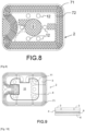
- an adhesive means 9 (adhesive layer) is deposited on one side of the substrate 6 carrying the antenna. figure 9 ) to secure it to the rear face 4b of the contact film 4.
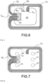
- a part 10 is cut out in the center of the antenna in order to allow the direct gluing of a chip 20 ( figure 10 ).
- the cutting of the opening can be done using a laser technique and simultaneously with that of the uncovered areas illustrated in the figure 5 .
- This type of cutting will allow the chip to be glued (soldered) directly onto the dielectric (rear face 4b - figure 1 ) of the contact-carrying film.
- the adhesion of the chip will not be dampened by the additional dielectric and adhesive layers.
- the final thickness of the product will be reduced due to the absence of intermediate layers between the chip and the contact film.
- this cutout forms an area which serves as a visual reference and physically delimits the deposition of the protective layer 21 for the chip and the connections.
- the resin or the coating material will benefit from good adhesion on the dielectrics known to those skilled in the art and controlled by the type of film.
- the dielectric is open only at the weld wells.
- figure 7 illustrates the perforations 11 made at the substrate level revealing solder wells. The latter will be used to connect the chip to the contact pads according to a technique known to those skilled in the art. The number of solder wells will be chosen according to the application.
- FIG 8 illustrates another variant which is not according to the invention where the perforations 12 are distributed around a central crimp 8.
- the antennas thus formed can be glued to the contact film, as illustrated in figure 9
- the support is cut to the format compatible with the assembly, Super 35mm film format known to those skilled in the art for example, to constitute the Dual Interface film.
- the steps described above can be adapted by a person skilled in the art in the case of a single-sided antenna.
- the single-sided film can be a simple grid complexed with a dielectric.
- the antenna can also be made up of two surfaces with a geometry and dimensions chosen to achieve capacitive coupling with a booster antenna placed at the heart of the card.
- the areas will be positioned for example around the integrated circuit or chip.
- the method according to the invention as well as the electronic module obtained by its implementation have in particular the advantage of reducing manufacturing costs and flexibility in the design of the antennas.
Landscapes
- Engineering & Computer Science (AREA)
- Microelectronics & Electronic Packaging (AREA)
- Computer Hardware Design (AREA)
- Physics & Mathematics (AREA)
- General Physics & Mathematics (AREA)
- Theoretical Computer Science (AREA)
- Computer Networks & Wireless Communication (AREA)
- Details Of Aerials (AREA)
- Printing Elements For Providing Electric Connections Between Printed Circuits (AREA)
Claims (11)
- - Verfahren zur Herstellung eines elektronischen Moduls, das zur Implementierung in ein duales tragbares Objekt bestimmt ist, wobei das Verfahren mindestens die folgenden Schritte umfasst:- die Verwendung einer einseitigen Folie (4), die aus einem oder mehreren Kontaktbereichen (3) und einer dielektrischen Schicht (5) mit einer oder mehreren Öffnungen (50) besteht,- die Verwendung eines einzelnen Substrats (6), das einen oder mehrere elektrisch leitende Bereiche (7) für die kontaktlose Kommunikation des Objekts und mindestens ein Kontaktpad (7p1, 7p2) umfasst,- die feste Verbindung der einseitigen Folie (4) mit dem Substrat (6) über eine Klebschicht (9), um einen Trägerstapel (4, 6, 9) des Moduls zu bilden, wobei der Trägerstapel (4, 6, 9) aus der einseitigen Folie (4), dem Substrat (6) und der Klebschicht (9) besteht,- die Positionierung einer integrierten Schaltung (20) und deren Verbindung mit den Kontaktbereichen (3) der einseitigen Folie und mindestens einem Kontaktpad (7p1, 7p2) von mindestens einem der elektrisch leitenden Bereiche (7),- das Aufbringen einer Schutzschicht (21) zumindest auf die integrierte Schaltung,- dadurch gekennzeichnet, dass man einen Bereich (10) in der Mitte von mindestens einem der elektrisch leitenden Bereiche (7) des Substrats (6) ausschneidet und die integrierte Schaltung (20) direkt auf die Rückseite (4b) der Folie (4) gegenüber der Seite (4a) der Folie mit den Kontakten (3) klebt.
- - Verfahren nach Anspruch 1, dadurch gekennzeichnet, dass das Substrat (6) mindestens einen elektrisch leitenden Bereich (7) umfasst, der aus Windungen besteht, wobei diese eine Antenne (71, 72) bilden und das mindestens eine Kontaktpad (7p1, 7p2) an mindestens einem Ende der Antenne angeordnet ist.
- - Verfahren nach Anspruch 1, dadurch gekennzeichnet, dass mindestens einer der elektrisch leitenden Bereiche (7) aus mindestens einer Leitermaterialfläche besteht.
- - Verfahren nach einem der vorhergehenden Ansprüche, dadurch gekennzeichnet, dass im Substrat (6) eine oder mehrere Öffnungen (52, 53) hergestellt werden, die den Öffnungen (50) in der Folie (4) entsprechen, um Lötvertiefungen zwischen der integrierten Schaltung (20) und den Kontaktbereichen (3) zu bilden.
- - Verfahren nach einem der Ansprüche 2 bis 4, dadurch gekennzeichnet, dass das Substrat (6) einen oder mehrere elektrisch leitende Bereiche (7) aus Aluminium aufweist, um die Antenne oder die Leitermaterialfläche zu bilden.
- - Verfahren nach einem der vorhergehenden Ansprüche, dadurch gekennzeichnet, dass das Muster des elektrisch leitenden Bereichs oder die Leitermaterialflächen unter Verwendung einer Ätztechnik, eines additiven Siebdruckverfahrens oder eines Übertragungsverfahrens hergestellt werden.
- - Elektronisches Modul (2), das dazu bestimmt ist, in einem tragbaren Gegenstand mit Kontaktfunktion implementiert zu werden, wobei das elektronische Modul mindestens folgende Elemente umfasst:• eine einseitige Folie (4) bestehend aus einem oder mehreren Kontaktbereichen (3) und einer dielektrischen Schicht (5) mit einer oder mehreren Öffnungen (50),• ein einzelnes Substrat (6) mit einem oder mehreren elektrisch leitenden Bereichen (7) für eine kontaktlose Kommunikation, wobei das Substrat (6) über eine Klebschicht (9) fest mit der einseitigen Folie (4) verbunden ist, um einen Trägerstapel (4, 6, 9) des Moduls zu bilden, wobei der Trägerstapel (4, 6, 9) aus der einseitigen Folie (4) und dem Substrat (6) und der Klebschicht (9) besteht;• mindestens einen elektrisch leitenden Bereich (7) mit mindestens einem Kontaktpad (7p1, 7p2, 8p1);• eine integrierte Schaltung (20), die mit den Kontaktbereichen (3) der einseitigen Folie (4) und mindestens einem Kontaktpad (7p1, 7p2) mindestens eines der elektrisch leitenden Bereiche (7) verbunden ist;• eine Schutzschicht (21) zumindest auf der integrierten Schaltung,• dadurch gekennzeichnet, dass das Substrat (6) in der Mitte des mindestens einen der elektrisch leitenden Bereiche (7) einen ausgesparten zentralen Bereich (10) mit einer Geometrie umfasst, die geeignet ist, die integrierte Schaltung (20) und die Schutzschicht (21) aufzunehmen, und dadurch dass die integrierte Schaltung (20) direkt auf die Rückseite (4b) der Folie (4) gegenüber der Seite (4a) der Folie (4) mit den Kontakten (3) geklebt ist.
- - Modul nach Anspruch 7, dadurch gekennzeichnet, dass mindestens einer der elektrisch leitenden Bereiche (7) in Form von Windungen (71, 72) vorliegt und sich darin das mindestens eine Anschlusspad (7p1, 7p2) an einem Ende befindet.
- - Modul nach Anspruch 7, dadurch gekennzeichnet, dass mindestens einer der elektrisch leitenden Bereiche (7) aus mindestens einer Leitermaterialfläche (75, 76) besteht.
- - Modul nach einem der Ansprüche 7 bis 9, dadurch gekennzeichnet, dass das Substrat (6) eine oder mehrere Perforationen (52, 53) den Öffnungen der einseitigen Folie entsprechend umfasst (4), um die Verbindung der integrierten Schaltung (20) mit den Kontaktbereichen herzustellen.
- - Modul nach einem der Ansprüche 7 bis 10, dadurch gekennzeichnet, dass die dielektrische Schicht (5) und/oder das Substrat (6) ausgewählt sind aus: Epoxydglasfaser, Polyethylen-Naphthalat PEN, Polyethylen-Terephthalat PET oder Polyvinylchlorid PVC.
Applications Claiming Priority (2)
| Application Number | Priority Date | Filing Date | Title |
|---|---|---|---|
| FR1860297A FR3088515B1 (fr) | 2018-11-08 | 2018-11-08 | Module electronique pour carte a puce |
| PCT/EP2019/077275 WO2020094320A1 (fr) | 2018-11-08 | 2019-10-09 | Module electronique pour carte a puce |
Publications (2)
| Publication Number | Publication Date |
|---|---|
| EP3877909A1 EP3877909A1 (de) | 2021-09-15 |
| EP3877909B1 true EP3877909B1 (de) | 2024-09-25 |
Family
ID=66286386
Family Applications (1)
| Application Number | Title | Priority Date | Filing Date |
|---|---|---|---|
| EP19780270.5A Active EP3877909B1 (de) | 2018-11-08 | 2019-10-09 | Elektronisches modul für chipkarte |
Country Status (10)
| Country | Link |
|---|---|
| US (1) | US12505329B2 (de) |
| EP (1) | EP3877909B1 (de) |
| JP (1) | JP7474251B2 (de) |
| KR (1) | KR20210087944A (de) |
| CN (1) | CN112930540A (de) |
| BR (1) | BR112021005517A2 (de) |
| ES (1) | ES3009672T3 (de) |
| FR (1) | FR3088515B1 (de) |
| SG (1) | SG11202103548XA (de) |
| WO (1) | WO2020094320A1 (de) |
Families Citing this family (5)
| Publication number | Priority date | Publication date | Assignee | Title |
|---|---|---|---|---|
| KR102914017B1 (ko) * | 2020-09-08 | 2026-01-19 | 엘지이노텍 주식회사 | 스마트 ic 기판, 스마트 ic 모듈 및 이를 포함하는 ic 카드 |
| JP7487401B2 (ja) * | 2021-02-17 | 2024-05-20 | 富士通フロンテック株式会社 | Rfidタグ |
| FR3131412B1 (fr) * | 2021-12-24 | 2024-01-05 | Wisekey Semiconductors | Module sans contact ayant une bobine d'antenne configurable |
| FR3131411B1 (fr) * | 2021-12-24 | 2024-01-05 | Wisekey Semiconductors | Procédé de fabrication d’un module sans contact ayant une bobine d'antenne à inductance finement ajustable |
| FR3150614A1 (fr) * | 2023-06-29 | 2025-01-03 | Paragon Identification | Radio-étiquette UHF et procédé de fabrication associé |
Family Cites Families (26)
| Publication number | Priority date | Publication date | Assignee | Title |
|---|---|---|---|---|
| US5483100A (en) * | 1992-06-02 | 1996-01-09 | Amkor Electronics, Inc. | Integrated circuit package with via interconnections formed in a substrate |
| FR2769390B1 (fr) * | 1997-10-08 | 2003-02-14 | Gemplus Card Int | Procede de fabrication de cartes a puce aptes a assurer un fonctionnement a contact et sans contact, et de cartes a puce sans contact |
| FR2801707B1 (fr) | 1999-11-29 | 2002-02-15 | A S K | Procede de fabrication d'une carte a puce hybride contact- sans contact avec un support d'antenne en materiau fibreux |
| JP4684433B2 (ja) * | 2001-02-07 | 2011-05-18 | 大日本印刷株式会社 | 接触・非接触兼用型icモジュールとその製造方法 |
| JP4734742B2 (ja) * | 2001-03-29 | 2011-07-27 | 大日本印刷株式会社 | Icモジュールとその製造方法 |
| JP4783997B2 (ja) * | 2001-05-11 | 2011-09-28 | 大日本印刷株式会社 | 接触・非接触兼用型icモジュールとその製造方法 |
| FR2829857B1 (fr) * | 2001-09-14 | 2004-09-17 | A S K | Carte a puce sans contact ou hybride contact-sans contact a tenue renforcee du module electronique |
| KR20030024132A (ko) * | 2001-09-17 | 2003-03-26 | (주)제이티 | 점착성 기판을 이용한 비접촉 ic 카드 및 그 제조방법 |
| DE10356153B4 (de) | 2003-12-02 | 2010-01-14 | Infineon Technologies Ag | Modul für kontaktlose Chipkarten oder Identifizierungssysteme |
| JP4387887B2 (ja) * | 2004-07-08 | 2009-12-24 | 株式会社ティーアイビーシー | 接触式icカード用テープキャリア |
| US8030746B2 (en) * | 2008-02-08 | 2011-10-04 | Infineon Technologies Ag | Integrated circuit package |
| WO2011157693A1 (en) * | 2010-06-18 | 2011-12-22 | Fci | Multi-layered flexible printed circuit and method of manufacture |
| EP2463809A1 (de) * | 2010-12-07 | 2012-06-13 | NagraID S.A. | Elektronische Karte mit elektrischem Kontakt, die eine elektronische Einheit und/oder eine Antenne umfasst |
| US9622359B2 (en) * | 2011-08-08 | 2017-04-11 | Féinics Amatech Teoranta | RFID transponder chip modules |
| US11928537B2 (en) * | 2013-01-18 | 2024-03-12 | Amatech Group Limited | Manufacturing metal inlays for dual interface metal cards |
| US11386317B2 (en) * | 2013-01-18 | 2022-07-12 | Amatech Group Limited | Transponder chip module with module antenna(s) and coupling frame(s) |
| US11341389B2 (en) * | 2013-01-18 | 2022-05-24 | Amatech Group Limited | Manufacturing metal inlays for dual interface metal cards |
| US11551051B2 (en) * | 2013-01-18 | 2023-01-10 | Amatech Group Limiied | Coupling frames for smartcards with various module opening shapes |
| FR3006551B1 (fr) * | 2013-05-30 | 2016-12-09 | Linxens Holding | Procede de fabrication d'un circuit imprime, circuit imprime obtenu par ce procede et module electronique comportant un tel circuit imprime |
| EP2811428A1 (de) * | 2013-06-07 | 2014-12-10 | Gemalto SA | Herstellungsverfahren einer Funkvorrichtung mit Aufrechterhaltung einer anisotropen Verbindung |
| US9424507B2 (en) * | 2014-04-01 | 2016-08-23 | Nxp B.V. | Dual interface IC card components and method for manufacturing the dual-interface IC card components |
| DE102014106062B4 (de) * | 2014-04-30 | 2018-11-22 | Infineon Technologies Ag | Chipkartenmodul, Chipkartenkörper, Chipkarte und Chipkartenherstellungsverfahren |
| JP2015219878A (ja) * | 2014-05-21 | 2015-12-07 | 凸版印刷株式会社 | 複合icカード及びそれに用いる複合icカード用モジュール |
| FR3026529B1 (fr) * | 2014-09-30 | 2017-12-29 | Linxens Holding | Procede de fabrication de carte a puce et carte a puce obtenue par ce procede. |
| JP2016212778A (ja) * | 2015-05-13 | 2016-12-15 | 凸版印刷株式会社 | デュアルインターフェース通信媒体 |
| DE102016114199B4 (de) * | 2016-08-01 | 2021-07-22 | Infineon Technologies Ag | Chipkartenmodul, chipkarte, chipkartenanordnung, verfahren zum ausbilden eines chipkartenmoduls und verfahren zum ausbilden einer chipkarte |
-
2018
- 2018-11-08 FR FR1860297A patent/FR3088515B1/fr active Active
-
2019
- 2019-10-09 SG SG11202103548XA patent/SG11202103548XA/en unknown
- 2019-10-09 US US17/292,235 patent/US12505329B2/en active Active
- 2019-10-09 WO PCT/EP2019/077275 patent/WO2020094320A1/fr not_active Ceased
- 2019-10-09 KR KR1020217013471A patent/KR20210087944A/ko not_active Ceased
- 2019-10-09 ES ES19780270T patent/ES3009672T3/es active Active
- 2019-10-09 JP JP2021525330A patent/JP7474251B2/ja active Active
- 2019-10-09 BR BR112021005517-7A patent/BR112021005517A2/pt unknown
- 2019-10-09 EP EP19780270.5A patent/EP3877909B1/de active Active
- 2019-10-09 CN CN201980071664.8A patent/CN112930540A/zh active Pending
Also Published As
| Publication number | Publication date |
|---|---|
| CN112930540A (zh) | 2021-06-08 |
| SG11202103548XA (en) | 2021-05-28 |
| BR112021005517A2 (pt) | 2021-06-29 |
| WO2020094320A1 (fr) | 2020-05-14 |
| US20210406636A1 (en) | 2021-12-30 |
| ES3009672T3 (en) | 2025-03-31 |
| JP2022507119A (ja) | 2022-01-18 |
| FR3088515B1 (fr) | 2022-01-28 |
| JP7474251B2 (ja) | 2024-04-24 |
| FR3088515A1 (fr) | 2020-05-15 |
| EP3877909A1 (de) | 2021-09-15 |
| US12505329B2 (en) | 2025-12-23 |
| KR20210087944A (ko) | 2021-07-13 |
Similar Documents
| Publication | Publication Date | Title |
|---|---|---|
| WO2020094320A1 (fr) | Module electronique pour carte a puce | |
| EP3567527B1 (de) | Herstellungsverfahren eines schaltkreises für chipkartenmodul, und schaltkreis für chipkartenmodul | |
| EP0424263B1 (de) | Chipkartensystem mit getrennter tragbarer elektronischer Einheit | |
| FR3003723A1 (fr) | Procede de fabrication d'un circuit imprime flexible, circuit imprime flexible obtenu par ce procede et module de carte a puce comportant un tel circuit imprime flexible | |
| EP3005846A1 (de) | Verfahren zur herstellung einer bestückten schaltung, in diesem verfahren hergestellte bestückte schaltung und elektronisches modul mit solch einer bestückten schaltung | |
| EP3408799B1 (de) | Verfahren zur herstellung eines chipkartenmoduls und chipkarte | |
| WO2014111656A1 (fr) | Systeme d'antenne pour microcircuit sans contact | |
| EP2915104B1 (de) | Verfahren zur herstellung einer anschlussvorrichtung für das modul einer smart card, durch das verfahren erhaltene anschlussvorrichtung und modul mit smart card anschlussvorrichtung | |
| WO1998057298A1 (fr) | Procede de fabrication de carte a puce sans contact | |
| EP3853773B1 (de) | Verfahren zur herstellung eines elektronischen moduls für ein tragbares objekt | |
| EP3391460A1 (de) | Einseitiges antennenmodul mit cms-vorrichtung | |
| FR3083892A1 (fr) | Carte a puce a double interface de communication et son procede de fabrication | |
| EP3853775B1 (de) | Verfahren zur herstellung eines kartenmoduls und hergestelltes modul | |
| EP3853774B1 (de) | Verfahren zum verbinden einer integrierten schaltung mit einer elektrischen schaltung | |
| FR2795202A1 (fr) | Carte et procede de fabrication de cartes ayant une interface de communication a contact et sans contact | |
| EP2608114A1 (de) | Verfahren zur Herstellung eines durch ein Plättchen geschützten Chip-Moduls eines integrierten Schaltkreises | |
| WO2014075869A1 (fr) | Procede de fabrication d'un module a puce electronique anti-charge electrostatique | |
| EP2631849A1 (de) | Verfahren zur Herstellung einer Vorrichtung, die ein mit einem elektrischen und/oder elektronischen Schaltkreis ausgestattetes Modul umfasst | |
| FR3005391A1 (fr) | Procede de fabrication d'un circuit flexible pour module de carte a puce, circuit flexible de carte a puce otenu par ce procede et module de carte a puce comportant un tel circuit flexible | |
| EP2189928A1 (de) | Vorrichtung mit integriertem Schaltkreis, die mit verschiedenen Kontaktflächen ausgestattet ist |
Legal Events
| Date | Code | Title | Description |
|---|---|---|---|
| STAA | Information on the status of an ep patent application or granted ep patent |
Free format text: STATUS: UNKNOWN |
|
| STAA | Information on the status of an ep patent application or granted ep patent |
Free format text: STATUS: THE INTERNATIONAL PUBLICATION HAS BEEN MADE |
|
| PUAI | Public reference made under article 153(3) epc to a published international application that has entered the european phase |
Free format text: ORIGINAL CODE: 0009012 |
|
| STAA | Information on the status of an ep patent application or granted ep patent |
Free format text: STATUS: REQUEST FOR EXAMINATION WAS MADE |
|
| 17P | Request for examination filed |
Effective date: 20210416 |
|
| AK | Designated contracting states |
Kind code of ref document: A1 Designated state(s): AL AT BE BG CH CY CZ DE DK EE ES FI FR GB GR HR HU IE IS IT LI LT LU LV MC MK MT NL NO PL PT RO RS SE SI SK SM TR |
|
| DAV | Request for validation of the european patent (deleted) | ||
| DAX | Request for extension of the european patent (deleted) | ||
| STAA | Information on the status of an ep patent application or granted ep patent |
Free format text: STATUS: EXAMINATION IS IN PROGRESS |
|
| 17Q | First examination report despatched |
Effective date: 20220513 |
|
| GRAP | Despatch of communication of intention to grant a patent |
Free format text: ORIGINAL CODE: EPIDOSNIGR1 |
|
| STAA | Information on the status of an ep patent application or granted ep patent |
Free format text: STATUS: GRANT OF PATENT IS INTENDED |
|
| INTG | Intention to grant announced |
Effective date: 20240426 |
|
| GRAS | Grant fee paid |
Free format text: ORIGINAL CODE: EPIDOSNIGR3 |
|
| GRAA | (expected) grant |
Free format text: ORIGINAL CODE: 0009210 |
|
| STAA | Information on the status of an ep patent application or granted ep patent |
Free format text: STATUS: THE PATENT HAS BEEN GRANTED |
|
| AK | Designated contracting states |
Kind code of ref document: B1 Designated state(s): AL AT BE BG CH CY CZ DE DK EE ES FI FR GB GR HR HU IE IS IT LI LT LU LV MC MK MT NL NO PL PT RO RS SE SI SK SM TR |
|
| REG | Reference to a national code |
Ref country code: GB Ref legal event code: FG4D Free format text: NOT ENGLISH |
|
| REG | Reference to a national code |
Ref country code: CH Ref legal event code: EP |
|
| REG | Reference to a national code |
Ref country code: DE Ref legal event code: R096 Ref document number: 602019059468 Country of ref document: DE |
|
| REG | Reference to a national code |
Ref country code: IE Ref legal event code: FG4D Free format text: LANGUAGE OF EP DOCUMENT: FRENCH |
|
| REG | Reference to a national code |
Ref country code: LT Ref legal event code: MG9D |
|
| PG25 | Lapsed in a contracting state [announced via postgrant information from national office to epo] |
Ref country code: NO Free format text: LAPSE BECAUSE OF FAILURE TO SUBMIT A TRANSLATION OF THE DESCRIPTION OR TO PAY THE FEE WITHIN THE PRESCRIBED TIME-LIMIT Effective date: 20241225 |
|
| PG25 | Lapsed in a contracting state [announced via postgrant information from national office to epo] |
Ref country code: GR Free format text: LAPSE BECAUSE OF FAILURE TO SUBMIT A TRANSLATION OF THE DESCRIPTION OR TO PAY THE FEE WITHIN THE PRESCRIBED TIME-LIMIT Effective date: 20241226 Ref country code: FI Free format text: LAPSE BECAUSE OF FAILURE TO SUBMIT A TRANSLATION OF THE DESCRIPTION OR TO PAY THE FEE WITHIN THE PRESCRIBED TIME-LIMIT Effective date: 20240925 |
|
| PG25 | Lapsed in a contracting state [announced via postgrant information from national office to epo] |
Ref country code: BG Free format text: LAPSE BECAUSE OF FAILURE TO SUBMIT A TRANSLATION OF THE DESCRIPTION OR TO PAY THE FEE WITHIN THE PRESCRIBED TIME-LIMIT Effective date: 20240925 |
|
| PG25 | Lapsed in a contracting state [announced via postgrant information from national office to epo] |
Ref country code: LV Free format text: LAPSE BECAUSE OF FAILURE TO SUBMIT A TRANSLATION OF THE DESCRIPTION OR TO PAY THE FEE WITHIN THE PRESCRIBED TIME-LIMIT Effective date: 20240925 |
|
| PG25 | Lapsed in a contracting state [announced via postgrant information from national office to epo] |
Ref country code: RS Free format text: LAPSE BECAUSE OF FAILURE TO SUBMIT A TRANSLATION OF THE DESCRIPTION OR TO PAY THE FEE WITHIN THE PRESCRIBED TIME-LIMIT Effective date: 20241225 |
|
| REG | Reference to a national code |
Ref country code: NL Ref legal event code: MP Effective date: 20240925 |
|
| PG25 | Lapsed in a contracting state [announced via postgrant information from national office to epo] |
Ref country code: RS Free format text: LAPSE BECAUSE OF FAILURE TO SUBMIT A TRANSLATION OF THE DESCRIPTION OR TO PAY THE FEE WITHIN THE PRESCRIBED TIME-LIMIT Effective date: 20241225 Ref country code: NO Free format text: LAPSE BECAUSE OF FAILURE TO SUBMIT A TRANSLATION OF THE DESCRIPTION OR TO PAY THE FEE WITHIN THE PRESCRIBED TIME-LIMIT Effective date: 20241225 Ref country code: LV Free format text: LAPSE BECAUSE OF FAILURE TO SUBMIT A TRANSLATION OF THE DESCRIPTION OR TO PAY THE FEE WITHIN THE PRESCRIBED TIME-LIMIT Effective date: 20240925 Ref country code: GR Free format text: LAPSE BECAUSE OF FAILURE TO SUBMIT A TRANSLATION OF THE DESCRIPTION OR TO PAY THE FEE WITHIN THE PRESCRIBED TIME-LIMIT Effective date: 20241226 Ref country code: FI Free format text: LAPSE BECAUSE OF FAILURE TO SUBMIT A TRANSLATION OF THE DESCRIPTION OR TO PAY THE FEE WITHIN THE PRESCRIBED TIME-LIMIT Effective date: 20240925 Ref country code: BG Free format text: LAPSE BECAUSE OF FAILURE TO SUBMIT A TRANSLATION OF THE DESCRIPTION OR TO PAY THE FEE WITHIN THE PRESCRIBED TIME-LIMIT Effective date: 20240925 |
|
| PG25 | Lapsed in a contracting state [announced via postgrant information from national office to epo] |
Ref country code: NL Free format text: LAPSE BECAUSE OF FAILURE TO SUBMIT A TRANSLATION OF THE DESCRIPTION OR TO PAY THE FEE WITHIN THE PRESCRIBED TIME-LIMIT Effective date: 20240925 |
|
| REG | Reference to a national code |
Ref country code: ES Ref legal event code: FG2A Ref document number: 3009672 Country of ref document: ES Kind code of ref document: T3 Effective date: 20250331 |
|
| PG25 | Lapsed in a contracting state [announced via postgrant information from national office to epo] |
Ref country code: IS Free format text: LAPSE BECAUSE OF FAILURE TO SUBMIT A TRANSLATION OF THE DESCRIPTION OR TO PAY THE FEE WITHIN THE PRESCRIBED TIME-LIMIT Effective date: 20250125 Ref country code: PT Free format text: LAPSE BECAUSE OF FAILURE TO SUBMIT A TRANSLATION OF THE DESCRIPTION OR TO PAY THE FEE WITHIN THE PRESCRIBED TIME-LIMIT Effective date: 20250127 |
|
| PG25 | Lapsed in a contracting state [announced via postgrant information from national office to epo] |
Ref country code: RO Free format text: LAPSE BECAUSE OF FAILURE TO SUBMIT A TRANSLATION OF THE DESCRIPTION OR TO PAY THE FEE WITHIN THE PRESCRIBED TIME-LIMIT Effective date: 20240925 Ref country code: SM Free format text: LAPSE BECAUSE OF FAILURE TO SUBMIT A TRANSLATION OF THE DESCRIPTION OR TO PAY THE FEE WITHIN THE PRESCRIBED TIME-LIMIT Effective date: 20240925 |
|
| PG25 | Lapsed in a contracting state [announced via postgrant information from national office to epo] |
Ref country code: EE Free format text: LAPSE BECAUSE OF FAILURE TO SUBMIT A TRANSLATION OF THE DESCRIPTION OR TO PAY THE FEE WITHIN THE PRESCRIBED TIME-LIMIT Effective date: 20240925 |
|
| PG25 | Lapsed in a contracting state [announced via postgrant information from national office to epo] |
Ref country code: CZ Free format text: LAPSE BECAUSE OF FAILURE TO SUBMIT A TRANSLATION OF THE DESCRIPTION OR TO PAY THE FEE WITHIN THE PRESCRIBED TIME-LIMIT Effective date: 20240925 Ref country code: PL Free format text: LAPSE BECAUSE OF FAILURE TO SUBMIT A TRANSLATION OF THE DESCRIPTION OR TO PAY THE FEE WITHIN THE PRESCRIBED TIME-LIMIT Effective date: 20240925 |
|
| PG25 | Lapsed in a contracting state [announced via postgrant information from national office to epo] |
Ref country code: SK Free format text: LAPSE BECAUSE OF FAILURE TO SUBMIT A TRANSLATION OF THE DESCRIPTION OR TO PAY THE FEE WITHIN THE PRESCRIBED TIME-LIMIT Effective date: 20240925 |
|
| REG | Reference to a national code |
Ref country code: CH Ref legal event code: PL |
|
| REG | Reference to a national code |
Ref country code: DE Ref legal event code: R097 Ref document number: 602019059468 Country of ref document: DE |
|
| PG25 | Lapsed in a contracting state [announced via postgrant information from national office to epo] |
Ref country code: MC Free format text: LAPSE BECAUSE OF FAILURE TO SUBMIT A TRANSLATION OF THE DESCRIPTION OR TO PAY THE FEE WITHIN THE PRESCRIBED TIME-LIMIT Effective date: 20240925 |
|
| PG25 | Lapsed in a contracting state [announced via postgrant information from national office to epo] |
Ref country code: DK Free format text: LAPSE BECAUSE OF FAILURE TO SUBMIT A TRANSLATION OF THE DESCRIPTION OR TO PAY THE FEE WITHIN THE PRESCRIBED TIME-LIMIT Effective date: 20240925 |
|
| PG25 | Lapsed in a contracting state [announced via postgrant information from national office to epo] |
Ref country code: LU Free format text: LAPSE BECAUSE OF NON-PAYMENT OF DUE FEES Effective date: 20241009 Ref country code: BE Free format text: LAPSE BECAUSE OF NON-PAYMENT OF DUE FEES Effective date: 20241031 |
|
| PG25 | Lapsed in a contracting state [announced via postgrant information from national office to epo] |
Ref country code: CH Free format text: LAPSE BECAUSE OF NON-PAYMENT OF DUE FEES Effective date: 20241031 |
|
| PLBE | No opposition filed within time limit |
Free format text: ORIGINAL CODE: 0009261 |
|
| STAA | Information on the status of an ep patent application or granted ep patent |
Free format text: STATUS: NO OPPOSITION FILED WITHIN TIME LIMIT |
|
| REG | Reference to a national code |
Ref country code: BE Ref legal event code: MM Effective date: 20241031 |
|
| 26N | No opposition filed |
Effective date: 20250626 |
|
| PG25 | Lapsed in a contracting state [announced via postgrant information from national office to epo] |
Ref country code: SE Free format text: LAPSE BECAUSE OF FAILURE TO SUBMIT A TRANSLATION OF THE DESCRIPTION OR TO PAY THE FEE WITHIN THE PRESCRIBED TIME-LIMIT Effective date: 20240925 |
|
| PGFP | Annual fee paid to national office [announced via postgrant information from national office to epo] |
Ref country code: IT Payment date: 20250923 Year of fee payment: 7 |
|
| REG | Reference to a national code |
Ref country code: AT Ref legal event code: UEP Ref document number: 1727270 Country of ref document: AT Kind code of ref document: T Effective date: 20240925 |
|
| PGFP | Annual fee paid to national office [announced via postgrant information from national office to epo] |
Ref country code: GB Payment date: 20250923 Year of fee payment: 7 |
|
| PGFP | Annual fee paid to national office [announced via postgrant information from national office to epo] |
Ref country code: FR Payment date: 20250923 Year of fee payment: 7 |
|
| PG25 | Lapsed in a contracting state [announced via postgrant information from national office to epo] |
Ref country code: IE Free format text: LAPSE BECAUSE OF NON-PAYMENT OF DUE FEES Effective date: 20241009 |
|
| PGFP | Annual fee paid to national office [announced via postgrant information from national office to epo] |
Ref country code: DE Payment date: 20250923 Year of fee payment: 7 |
|
| PGFP | Annual fee paid to national office [announced via postgrant information from national office to epo] |
Ref country code: AT Payment date: 20250926 Year of fee payment: 7 |
|
| PG25 | Lapsed in a contracting state [announced via postgrant information from national office to epo] |
Ref country code: HR Free format text: LAPSE BECAUSE OF FAILURE TO SUBMIT A TRANSLATION OF THE DESCRIPTION OR TO PAY THE FEE WITHIN THE PRESCRIBED TIME-LIMIT Effective date: 20240925 |
|
| PG25 | Lapsed in a contracting state [announced via postgrant information from national office to epo] |
Ref country code: CY Free format text: LAPSE BECAUSE OF FAILURE TO SUBMIT A TRANSLATION OF THE DESCRIPTION OR TO PAY THE FEE WITHIN THE PRESCRIBED TIME-LIMIT; INVALID AB INITIO Effective date: 20191009 |
|
| PGFP | Annual fee paid to national office [announced via postgrant information from national office to epo] |
Ref country code: ES Payment date: 20251103 Year of fee payment: 7 |
|
| PG25 | Lapsed in a contracting state [announced via postgrant information from national office to epo] |
Ref country code: HU Free format text: LAPSE BECAUSE OF FAILURE TO SUBMIT A TRANSLATION OF THE DESCRIPTION OR TO PAY THE FEE WITHIN THE PRESCRIBED TIME-LIMIT; INVALID AB INITIO Effective date: 20191009 |