EP4002486A1 - Verfahren zur herstellung eines mit einer mikroelektronischen vorrichtung dotierten bereichs - Google Patents
Verfahren zur herstellung eines mit einer mikroelektronischen vorrichtung dotierten bereichs Download PDFInfo
- Publication number
- EP4002486A1 EP4002486A1 EP21208507.0A EP21208507A EP4002486A1 EP 4002486 A1 EP4002486 A1 EP 4002486A1 EP 21208507 A EP21208507 A EP 21208507A EP 4002486 A1 EP4002486 A1 EP 4002486A1
- Authority
- EP
- European Patent Office
- Prior art keywords
- active layer
- modified
- semiconductor material
- layer
- doped zone
- Prior art date
- Legal status (The legal status is an assumption and is not a legal conclusion. Google has not performed a legal analysis and makes no representation as to the accuracy of the status listed.)
- Pending
Links
Images
Classifications
-
- H—ELECTRICITY
- H10—SEMICONDUCTOR DEVICES; ELECTRIC SOLID-STATE DEVICES NOT OTHERWISE PROVIDED FOR
- H10D—INORGANIC ELECTRIC SEMICONDUCTOR DEVICES
- H10D30/00—Field-effect transistors [FET]
- H10D30/01—Manufacture or treatment
- H10D30/021—Manufacture or treatment of FETs having insulated gates [IGFET]
- H10D30/031—Manufacture or treatment of FETs having insulated gates [IGFET] of thin-film transistors [TFT]
- H10D30/0321—Manufacture or treatment of FETs having insulated gates [IGFET] of thin-film transistors [TFT] comprising silicon, e.g. amorphous silicon or polysilicon
- H10D30/0323—Manufacture or treatment of FETs having insulated gates [IGFET] of thin-film transistors [TFT] comprising silicon, e.g. amorphous silicon or polysilicon comprising monocrystalline silicon
-
- H—ELECTRICITY
- H10—SEMICONDUCTOR DEVICES; ELECTRIC SOLID-STATE DEVICES NOT OTHERWISE PROVIDED FOR
- H10P—GENERIC PROCESSES OR APPARATUS FOR THE MANUFACTURE OR TREATMENT OF DEVICES COVERED BY CLASS H10
- H10P32/00—Diffusion of dopants within, into or out of wafers, substrates or parts of devices
- H10P32/10—Diffusion of dopants within, into or out of semiconductor bodies or layers
- H10P32/17—Diffusion of dopants within, into or out of semiconductor bodies or layers characterised by the semiconductor material
- H10P32/171—Diffusion of dopants within, into or out of semiconductor bodies or layers characterised by the semiconductor material being group IV material
-
- H—ELECTRICITY
- H10—SEMICONDUCTOR DEVICES; ELECTRIC SOLID-STATE DEVICES NOT OTHERWISE PROVIDED FOR
- H10D—INORGANIC ELECTRIC SEMICONDUCTOR DEVICES
- H10D30/00—Field-effect transistors [FET]
- H10D30/60—Insulated-gate field-effect transistors [IGFET]
- H10D30/67—Thin-film transistors [TFT]
- H10D30/6704—Thin-film transistors [TFT] having supplementary regions or layers in the thin films or in the insulated bulk substrates for controlling properties of the device
- H10D30/6713—Thin-film transistors [TFT] having supplementary regions or layers in the thin films or in the insulated bulk substrates for controlling properties of the device characterised by the properties of the source or drain regions, e.g. compositions or sectional shapes
-
- H—ELECTRICITY
- H10—SEMICONDUCTOR DEVICES; ELECTRIC SOLID-STATE DEVICES NOT OTHERWISE PROVIDED FOR
- H10D—INORGANIC ELECTRIC SEMICONDUCTOR DEVICES
- H10D30/00—Field-effect transistors [FET]
- H10D30/60—Insulated-gate field-effect transistors [IGFET]
- H10D30/67—Thin-film transistors [TFT]
- H10D30/674—Thin-film transistors [TFT] characterised by the active materials
- H10D30/6741—Group IV materials, e.g. germanium or silicon carbide
- H10D30/6743—Silicon
- H10D30/6744—Monocrystalline silicon
-
- H—ELECTRICITY
- H10—SEMICONDUCTOR DEVICES; ELECTRIC SOLID-STATE DEVICES NOT OTHERWISE PROVIDED FOR
- H10P—GENERIC PROCESSES OR APPARATUS FOR THE MANUFACTURE OR TREATMENT OF DEVICES COVERED BY CLASS H10
- H10P14/00—Formation of materials, e.g. in the shape of layers or pillars
- H10P14/60—Formation of materials, e.g. in the shape of layers or pillars of insulating materials
- H10P14/69—Inorganic materials
- H10P14/692—Inorganic materials composed of oxides, glassy oxides or oxide-based glasses
- H10P14/6921—Inorganic materials composed of oxides, glassy oxides or oxide-based glasses containing silicon
- H10P14/69215—Inorganic materials composed of oxides, glassy oxides or oxide-based glasses containing silicon the material being a silicon oxide, e.g. SiO2
-
- H—ELECTRICITY
- H10—SEMICONDUCTOR DEVICES; ELECTRIC SOLID-STATE DEVICES NOT OTHERWISE PROVIDED FOR
- H10P—GENERIC PROCESSES OR APPARATUS FOR THE MANUFACTURE OR TREATMENT OF DEVICES COVERED BY CLASS H10
- H10P32/00—Diffusion of dopants within, into or out of wafers, substrates or parts of devices
- H10P32/10—Diffusion of dopants within, into or out of semiconductor bodies or layers
- H10P32/14—Diffusion of dopants within, into or out of semiconductor bodies or layers within a single semiconductor body or layer in a solid phase; between different semiconductor bodies or layers, both in a solid phase
- H10P32/1408—Diffusion of dopants within, into or out of semiconductor bodies or layers within a single semiconductor body or layer in a solid phase; between different semiconductor bodies or layers, both in a solid phase from or through or into an external applied layer, e.g. photoresist or nitride layers
- H10P32/141—Diffusion of dopants within, into or out of semiconductor bodies or layers within a single semiconductor body or layer in a solid phase; between different semiconductor bodies or layers, both in a solid phase from or through or into an external applied layer, e.g. photoresist or nitride layers the applied layer comprising oxides only
- H10P32/1412—Diffusion of dopants within, into or out of semiconductor bodies or layers within a single semiconductor body or layer in a solid phase; between different semiconductor bodies or layers, both in a solid phase from or through or into an external applied layer, e.g. photoresist or nitride layers the applied layer comprising oxides only through the applied layer
-
- H—ELECTRICITY
- H10—SEMICONDUCTOR DEVICES; ELECTRIC SOLID-STATE DEVICES NOT OTHERWISE PROVIDED FOR
- H10P—GENERIC PROCESSES OR APPARATUS FOR THE MANUFACTURE OR TREATMENT OF DEVICES COVERED BY CLASS H10
- H10P32/00—Diffusion of dopants within, into or out of wafers, substrates or parts of devices
- H10P32/10—Diffusion of dopants within, into or out of semiconductor bodies or layers
- H10P32/14—Diffusion of dopants within, into or out of semiconductor bodies or layers within a single semiconductor body or layer in a solid phase; between different semiconductor bodies or layers, both in a solid phase
- H10P32/1408—Diffusion of dopants within, into or out of semiconductor bodies or layers within a single semiconductor body or layer in a solid phase; between different semiconductor bodies or layers, both in a solid phase from or through or into an external applied layer, e.g. photoresist or nitride layers
- H10P32/1414—Diffusion of dopants within, into or out of semiconductor bodies or layers within a single semiconductor body or layer in a solid phase; between different semiconductor bodies or layers, both in a solid phase from or through or into an external applied layer, e.g. photoresist or nitride layers the applied layer being silicon, silicide or SIPOS, e.g. polysilicon or porous silicon
Definitions
- the present invention relates to the field of microelectronics. It finds for particularly advantageous application the production of sources and drains in transistors requiring low thermal budgets, in particular in the field of monolithic 3D integration.
- CoolCube TM integration process proposes to form transistors on top of each other in a sequential manner.
- a problem of this method concerns the management of the thermal budget during the formation of the upper layers of transistors.
- the formation of doped areas on either side of the transistor channel, typically the source and drain areas of the transistor conventionally requires a step of activation and/or diffusion of the dopants, after ion implantation of doping species.
- a conventional solution for the activation of dopants in the context of a planar technology consists in carrying out a high temperature thermal annealing, typically at a temperature T>1000° C., after implantation of the dopants.
- An existing solution for the activation of dopants within the framework of a 3D integration technology consists in amorphizing part of the semiconductor layer intended to form the source and drain zones, before or during the implantation of the dopants. .
- the activation of the dopants takes place during the solid phase recrystallization of the amorphous semiconductor layer. This recrystallization/activation step can be done at a lower temperature, typically at a temperature T ⁇ 600°C.
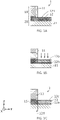
- the Figures 1A-1C present the stages of such a recrystallization process called SPER (acronym for “solid-phase epitaxial regrowth” according to the English terminology).
- the Figure 1A illustrates a device 1 intended to form a transistor and comprising a gate pattern 10 flanked by a spacer 11 on a substrate 20 of SOI type (acronym for “Silicon on Insulator” or “silicon on insulator” in French).
- the spacer 11 generally has dimensions ranging from 6 nm to 40 nm.
- the figure 1B illustrates a bombardment of ions at the edge of the spacer 11, suitable for partially amorphizing the upper silicon layer 12 (topSi) of the SOI substrate, and for implanting dopants in this amorphous part 12a.
- a crystalline part 12b of topSi layer 12 is retained after this bombardment, so as to form a seed for future recrystallization.
- the figure 1C illustrates the partial recrystallization of topSi from this seed 12b. During recrystallization, the dopants are incorporated and activated. This recrystallization ultimately makes it possible to obtain a doped zone 13.
- a drawback of this solution based on the SPER recrystallization process is that there is an undoped zone 12d between the channel 15 and the doped zone 13, under the spacer 11.
- This undoped zone 12d has a dimension along the axis y substantially identical to that of spacer 11.
- the presence of this undoped zone 12d has the effect of increasing the access resistance of the transistor.
- Another drawback is the presence of the undoped seed 12b underlying the doped zone 13. This further increases the access resistance of the transistor.
- good control of the depth of amorphization becomes essential. The implementation of the SPER process is therefore complex.
- the recrystallization of the amorphous part 12a of the topSi is generally not complete. A non-crystallized superficial residual layer 12c remains, it is then necessary to provide an etching to eliminate it.
- An object of the present invention is to overcome at least in part some of the drawbacks mentioned above.
- an object of the present invention is to provide a method of forming a doped zone improving the access resistance of a microelectronic device.
- the modification of the active layer is carried out so as to form a modified portion extending in at least one region of the active layer not surmounted by the grid pattern and extending as far as plumb with the at least a side flank of the grid pattern.
- the region of the active layer which is for its part surmounted by the grid pattern forms an unmodified portion.
- the interface between the modified portion and the unmodified portion is located to the right of the flank of the grid pattern.
- the modification of a portion of the active layer is carried out before the formation of the spacer. Consequently, no active layer portion is masked by the spacer during this modification.
- the interface between the modified portion and the unmodified portion plumb with the gate pattern extends substantially in extension of the sidewall, in the active layer. After removal of the modified portion, this interface forms the edge of the unmodified portion. The formation of the doped zone is done from this edge.
- the interface between the unmodified portion and the modified portion thus becomes a junction between the unmodified portion, typically the channel of the transistor, and the doped zone, typically the source or the drain of the transistor. This junction is preferably abrupt.
- Such a method advantageously eliminates the residual undoped zone which is located directly above the spacer, between the channel and the doped zone, when the known methods are implemented.
- the junction thus obtained makes it possible to reduce the access resistance of the transistor.
- a bombardment carried out within the framework of the known solutions does not make it possible to make the undoped zone disappear, even if this bombardment were modified so as to tilt the direction of bombardment.
- the formation of the doped zone by lateral epitaxy that is to say from the edge of the unmodified portion, also makes it possible to dispense with the need to keep an epitaxy seed under the modified portion.
- the modification can be carried out over the entire thickness of the active layer, so that the modified portion has a thickness equal to that of the active layer, and that, consequently, the doped zone has a thickness equal to that of the active layer. It is therefore not necessary to precisely control an implantation depth, unlike the known methods. This simplifies the process.
- a doped zone extending along the entire height of the active layer also makes it possible to reduce the access resistance of the transistor.
- Such a process can advantageously be implemented at low temperature, typically for temperatures T ⁇ 600°C. This process is thus compatible with a 3D integration technology.
- the term “over”, “overcomes”, “covers” or “underlying” or their equivalents do not necessarily mean “in contact with”.
- the deposition of a first layer on a second layer does not necessarily mean that the two layers are directly in contact with each other, but it does mean that the first layer at least partially covers the second layer. by being either directly in contact with it or by being separated from it by at least one other layer or at least one other element.
- a layer can also be composed of several sub-layers of the same material or of different materials.
- a substrate, a layer, a device, "based" on a material M is understood to mean a substrate, a layer, a device comprising: only this material M or this material M and possibly other materials, for example alloying elements, impurities or doping elements.
- a spacer based on silicon nitride SiN can for example comprise non-stoichiometric silicon nitride (SiN), or stoichiometric silicon nitride (Si3N4), or else a silicon oxy-nitride (SiON).
- a spacer forms a ring around the grid, with a closed contour; the description of a spacer preferably means this single spacer around the grid; however, the sectional illustrative drawings, generally along a plane transverse to the longitudinal direction of the grids, show two spacer parts on either side of the sides of the grid. By extension, these two spacer parts are often referred to as “the spacers”. This last terminology may possibly be adopted in this application. Furthermore, the invention extends to embodiments in which at least two discontinuous spacers cover a grid pattern.
- the present invention notably allows the manufacture of at least one transistor or of a plurality of transistors on a substrate.
- This substrate can be solid or "bulk” according to the English terminology, or even of the semiconductor on insulator type, for example a silicon on insulator SOI substrate (acronym for "silicon on insulator) or a germanium substrate on GeOI insulator (acronym for "germanium on insulator”).
- the invention can also be implemented more broadly for various microelectronic devices or components.
- microelectronic device any type of element made with the means of microelectronics.
- These devices include in particular, in addition to devices for purely electronic purposes, micromechanical or electromechanical devices (MEMS, NEMS, etc.) as well as optical or optoelectronic devices (MOEMS, etc.).
- MEMS micromechanical or electromechanical devices
- MOEMS optical or optoelectronic devices
- successive steps of the manufacturing process are described below.
- the adjective “successive” does not necessarily imply, even if this is generally preferred, that the stages follow each other immediately, intermediate stages possibly separating them.
- the term “step” means the performance of part of the method, and can designate a set of sub-steps.
- dielectric qualifies a material whose electrical conductivity is low enough in the given application to serve as an insulator.
- a dielectric material preferably has a dielectric constant of less than 7.
- the spacers are typically formed from a dielectric material.
- the modified semiconductor material is said to be different from the semiconductor material.
- selective etching with respect to or “etching having selectivity with respect to” an etching configured to remove a material A or a layer A with respect to a material B or d layer B, and having an etching speed of material A greater than the etching speed of material B.
- the selectivity is the ratio between the etching speed of material A over the etching speed of material B.
- thickness for a layer height for a device (transistor or gate for example) and depth for a cavity or an etching.
- the thickness is taken according to a direction normal to the main extension plane of the layer, the height and the depth are taken according to a direction normal to the base plane of the substrate.
- the main extension plane of the layer, respectively the base plane of the substrate is generally parallel to a lower face or an upper face of this layer, respectively of this substrate.
- a preferably orthonormal reference frame formed by the x, y, z axes is shown in the accompanying drawings.
- the substrate more precisely its lower face and/or its upper face, extend in the basal plane xy.
- the length is taken according to the direction carried by the x axis and the width is taken according to the direction carried by the y axis.
- An element located “straight from” or “straight from” another element means that these two elements are both located on the same line perpendicular to the basal plane, or on the same line oriented along the z axis in the figures.
- An element located “as an extension” of another element means that these two elements are both oriented in the same direction or the same plane, and preferably continuous with one another.
- “Horizontal” means an orientation parallel to an xy plane. “Vertical” means an orientation parallel to the z axis.
- a direction substantially normal to a plane means a direction having an angle of 90 ⁇ 10° relative to the plane.
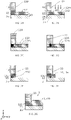
- FIG. 2A-2G A first embodiment of the method is illustrated in Figures 2A-2G .
- This method is preferably implemented on an initial structure comprising a grid pattern 10 and a substrate 20, as illustrated in figure 2A for example.
- the substrate 20 can typically be a substrate of the semiconductor on insulator type, for example a silicon on insulator SOI (acronym for the English "silicon on insulator) substrate or a germanium on insulator GeOI (acronym for the English "germanium on insulator).
- SOI silicon on insulator
- GeOI germanium on insulator
- the upper face 121 of the active layer 12 is surmounted by a grid stack or grid pattern 10.
- the grid pattern 10 may successively have the following layers arranged from the active layer 12: a layer of interface oxide (often referred to as gate oxide), a polycrystalline silicon gate called polySi and a hard mask.
- this gate pattern may comprise a layer with a high dielectric constant, called a “high k” layer surmounted by a metal gate.
- the grid pattern 10 typically has a height, along z, of several tens of nanometers to several hundreds of nanometers.
- the grid pattern will simply be designated grid 10.
- the invention also covers an alternative embodiment for which the grid pattern 10 is a sacrificial pattern intended to be removed after production. spacers, then to be replaced by another gate stack forming a gate 10. Such a process is commonly referred to as “gate last” according to Anglo-Saxon terminology.
- the gate 10 in the following therefore designates either a gate stack of the "gate first" type (the gate is kept after the spacers have been produced) or of the "gate last” type (the gate is replaced at the end of the from the production of the spacers).
- the active layer is designated topSi 12.
- the doped zone intended to form the source or the drain of the transistor is designated S/D zone 13.
- This modified portion 12m then has an interface 125 with the unmodified topSi portion 12e, which is covered by the gate 10. It is in the unmodified portion 12e that the channel 15 of the transistor will be formed later.
- the 125 interface between the modified 12m portion and the unmodified portion 12e is substantially parallel to z, in an extension of the flank 100 of the gate 10. This makes it possible to subsequently align the junction between the channel and the S/D zone of the transistor directly at the edge of the gate 10. This prevents an undoped portion from remaining between the channel 15 and the S/D zone subsequently formed.
- the access resistance to the transistor is then reduced.
- the modified portion 12m preferably has a thickness equal to the thickness of the active layer 12. This prevents an undoped portion from remaining outside the channel 15, under the S/D zone subsequently formed. The access resistance to the transistor is then reduced. Such a modified portion 12m thus extends as far as the interface 212 with the BOX 21. It is therefore not necessary to precisely control the in-depth stopping of the modification. In-depth control of the modification of the topSi is thus facilitated.
- the modification of the topSi 12 is configured to create a difference between the etching properties of the modified Si of the 12m portion and the crystalline Si of the channel 15. This modification can be carried out by ion implantation or by plasma. The modification is preferably carried out anisotropically, in a direction mainly directed along z. This therefore does not modify the portion 12e masked by the grid 10, in this direction z.
- This modification can be structural. It can induce a phase change of the crystalline active layer 12 so as to create an amorphous modified portion 12e. This modification is not intended to pulverize the topSi 12.
- any microelectronics step is preferably carried out at a temperature lower than the recrystallization temperature of the modified layer 12m.
- the layer deposited/etched after the amorphization can be deposited/etched at a temperature lower than the recrystallization temperature of the modified layer 12m.
- the deposition/etching temperature can be less than 700° C., preferably less than 600° C. and ideally less than 500° C. to avoid recrystallization of the amorphous silicon layer 12m.
- the deposition/etching temperature can be lower than 600° C., preferably lower than 500° C. and ideally lower than 400° C. to avoid recrystallization of the layer of amorphous germanium 12m.
- this modification can be chemical. It may include an introduction of chemical species aimed at modifying the etching properties and/or the nature of the semiconductor material.
- this anisotropic modification is carried out by anisotropic implantation of ions over at least the entire thickness of the topSi 12.
- This anisotropic modification can be carried out in an implanter or from a plasma.
- the anisotropic implantation can be carried out in a conventional implanter.
- the implantation angle remains constant throughout the implantation. This inclination is parallel to the side 100 of the grid 10.
- the implanted species can be, for example, silicon (Si), germanium (Ge), argon (Ar), oxygen (O) or nitrogen (N).
- the implantation conditions can be determined by simulation using a tool of the SRIM type (acronym for “Stopping and Range of Ions in Matter”) or TRIM (acronym for “Transport of ions in matter”).
- Spacer 11 is formed after modification of topSi 12 and preferably before removal of modified portion 12m.
- the spacer 11 is typically formed by depositing a layer 110 of a dielectric material on the gate 10 and on the active layer 12, preferably in a conformal manner ( Fig. 2C ).
- An anisotropic etching step along z then makes it possible to remove horizontal portions of said dielectric layer 110 at the top of gate 10 and on part of active layer 12, while retaining a vertical portion of dielectric layer on the side 100 of the grid 10. This vertical portion forms spacer 11.
- the dielectric layer can be made of silicon nitride SiN or SiCO (silicon carbon oxygen).
- the anisotropic etching aimed at forming the spacer 11 can be configured to stop at the level of the upper face 120 of the modified portion 12m ( 2D figure ). Stopping the etching on the upper face 120 of the modified portion 12m can be achieved by controlling the etching time, or by detecting the end of etching in a plasma reactor, or even by resorting to an etching solution having sufficient selectivity, for example greater than 10:1, between the dielectric material and the modified semiconductor material of the modified portion 12m.
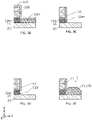
- the anisotropic etching aimed at forming the spacer 11 can be configured to also etch the modified portion 12m ( Figures 3B-3C ) not masked by the spacer 11.
- the etching solution preferably has little or no selectivity between the dielectric material and the modified semiconductor material. This saves one process step.
- an isotropic and selective etching step is preferably carried out. This isotropic and selective etching can have a selectivity greater than 10:1 between the modified semiconductor material and the semiconductor material. This makes it possible to remove the modified portion 12m under the spacer 11 while keeping the unmodified portion 12e, as illustrated in 3d figure .
- the anisotropic etching aimed at forming the spacer 11 is followed by anisotropic etching of the modified semiconductor material, for example amorphous silicon. This last etching is not necessarily selective with respect to the unmodified semiconductor material, for example crystalline silicon. It is then followed by an isotropic and selective etching of the modified semiconductor material with respect to the unmodified semiconductor material, to remove the modified portion 12m under the spacer 11.
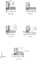
- a protective layer 111 a few nanometers thick, for example between 1 nm and 3 nm, can be deposited prior to the deposition of the dielectric layer 110 ( figure 4B ).
- the spacer 11' is therefore formed in two stages.
- a first anisotropic etching directed along z makes it possible to remove horizontal portions of dielectric layer 110 while retaining a vertical portion of dielectric layer 110 ( Fig. 4C ).
- a second etching makes it possible to remove horizontal portions of protective layer 111 while retaining a vertical portion of protective layer 111 ( 4D figure ).
- the protective layer 111 is used here to protect the modified portion 12m during the first anisotropic etching of the dielectric layer 110.
- the protective layer 110 can be made of silicon dioxide.
- the first etching can be done by plasma from fluorocarbon species.
- the second etching can be a wet etching based on diluted HF. Such a second etching has sufficient selectivity with respect to the modified semiconductor material. This second etching can alternatively be done by RIE reactive ion etching.
- the modified portion 12m is selectively removed from the unmodified portion 12e ( figures 2E , 3D , 4E ). This removal is typically done by selective etching of the modified semiconductor material with respect to the unmodified semiconductor material.
- the etch selectivity can be greater than or equal to 5:1, and preferably greater than or equal to 10:1.
- Methods for the selective etching of amorphous Si and Si alloys with respect to crystalline Si as described in the document "Low temperature catalyst enhanced etch process with high etch rate selectivity for amorphous silicon based alloys over single-crystalline silicon based alloys, M Bauer”, or in the document “SELECTIVE ETCHING OF AMORPHOUS SILICON OVER EPITAXIAL SILICON, US 9,991,129 B1 can be used to etch modified portion 12m selectively to unmodified portion 12e.
- This selective etching of amorphous Si can be carried out for example using a gaseous mixture containing chlorine atoms.
- the gas mixture is based on hydrochloric acid.
- the gas mixture is based on hydrochloric acid, germane and optionally dihydrogen.
- This selective etching makes it possible to expose a side 150 of the unmodified portion 12e.
- This flank 150 is substantially parallel to z, in an extension of the flank 100 of the gate 10.
- This flank 150 is advantageously used to form by lateral epitaxy, in a direction substantially normal to the flank 150, the doped zone 13.
- the flank 150 becomes consequently an interface forming a junction between the channel 15 and the doped zone 13.
- This junction is advantageously located directly at the edge of the gate 10, directly above the flank 100. The transistor access resistance can thus be reduced.
- the lateral epitaxy takes place from the flank 150, preferably only from the edge 150, first and mainly along the y axis (portion 13a of the doped zone 13 on the figure 2F ).
- This epitaxy of the doped zone 13 can continue partly along z (portion 13b of the doped zone 13 on the figures 2G , 3E , 4F ).
- RSD Read Only Device
- An in situ doped epitaxy process is preferably implemented to form the doped zone 13.
- a boron (:B) or phosphorus (:P) doping can thus be obtained.
- the doped zone 13 can for example be based on SiGe:B, Si:B or Si:P.
- a cavity is formed between the BOX 21 and the doped zone 13, 13b, during the lateral epitaxy. Such a cavity improves the electrical insulation between the doped zone 13 and the substrate underlying the BOX 21.
- a thin layer of silicon oxide is deposited on the gate pattern 10, then etched (for example using a chemistry based on HF ) to form a thin layer of silicon oxide only on the sides 100 of the gate.
- This layer of silicon oxide has a width less than or equal to 3 nm, preferably less than or equal to 1 nm. Given the small width of this layer, it cannot be likened to a spacer which generally has a width of 6nm to 40nm, allowing it to isolate Grid.
- the role of this thin layer of silicon oxide is to avoid a phenomenon of “lateral dispersion” or “lateral straggling” during the amorphization of the layer of topSi 12.
- side flank corresponding to the reference 100 in the figures may include this thin layer of silicon oxide.
- the gate pattern can thus comprise this thin layer of silicon oxide.
Landscapes
- Thin Film Transistor (AREA)
- Insulated Gate Type Field-Effect Transistor (AREA)
Applications Claiming Priority (1)
| Application Number | Priority Date | Filing Date | Title |
|---|---|---|---|
| FR2011822A FR3116379B1 (fr) | 2020-11-18 | 2020-11-18 | Procédé de fabrication d’une zone dopée d’un dispositif microélectronique |
Publications (1)
| Publication Number | Publication Date |
|---|---|
| EP4002486A1 true EP4002486A1 (de) | 2022-05-25 |
Family
ID=74668972
Family Applications (1)
| Application Number | Title | Priority Date | Filing Date |
|---|---|---|---|
| EP21208507.0A Pending EP4002486A1 (de) | 2020-11-18 | 2021-11-16 | Verfahren zur herstellung eines mit einer mikroelektronischen vorrichtung dotierten bereichs |
Country Status (3)
| Country | Link |
|---|---|
| US (1) | US11942323B2 (de) |
| EP (1) | EP4002486A1 (de) |
| FR (1) | FR3116379B1 (de) |
Citations (5)
| Publication number | Priority date | Publication date | Assignee | Title |
|---|---|---|---|---|
| US20080242037A1 (en) | 2007-03-28 | 2008-10-02 | Bernhard Sell | Semiconductor device having self-aligned epitaxial source and drain extensions |
| EP2765599A1 (de) * | 2013-02-11 | 2014-08-13 | Commissariat A L'energie Atomique Et Aux Energies Alternatives | Verfahren zur Herstellung eines Transistors |
| EP2835832A2 (de) | 2013-08-09 | 2015-02-11 | Commissariat à l'Énergie Atomique et aux Énergies Alternatives | Verbessertes Verfahren zur Herstellung von dotierten Zonen und/oder Zonen, die eine Spannung unter den Abstandhaltern eines Transistors ausüben |
| EP3144973A1 (de) * | 2015-09-18 | 2017-03-22 | Commissariat A L'energie Atomique Et Aux Energies Alternatives | Verfahren zur bildung von abstandhaltern eines gates eines transistors |
| US9991129B1 (en) | 2017-05-23 | 2018-06-05 | Applied Materials, Inc. | Selective etching of amorphous silicon over epitaxial silicon |
-
2020
- 2020-11-18 FR FR2011822A patent/FR3116379B1/fr active Active
-
2021
- 2021-11-16 EP EP21208507.0A patent/EP4002486A1/de active Pending
- 2021-11-18 US US17/455,436 patent/US11942323B2/en active Active
Patent Citations (5)
| Publication number | Priority date | Publication date | Assignee | Title |
|---|---|---|---|---|
| US20080242037A1 (en) | 2007-03-28 | 2008-10-02 | Bernhard Sell | Semiconductor device having self-aligned epitaxial source and drain extensions |
| EP2765599A1 (de) * | 2013-02-11 | 2014-08-13 | Commissariat A L'energie Atomique Et Aux Energies Alternatives | Verfahren zur Herstellung eines Transistors |
| EP2835832A2 (de) | 2013-08-09 | 2015-02-11 | Commissariat à l'Énergie Atomique et aux Énergies Alternatives | Verbessertes Verfahren zur Herstellung von dotierten Zonen und/oder Zonen, die eine Spannung unter den Abstandhaltern eines Transistors ausüben |
| EP3144973A1 (de) * | 2015-09-18 | 2017-03-22 | Commissariat A L'energie Atomique Et Aux Energies Alternatives | Verfahren zur bildung von abstandhaltern eines gates eines transistors |
| US9991129B1 (en) | 2017-05-23 | 2018-06-05 | Applied Materials, Inc. | Selective etching of amorphous silicon over epitaxial silicon |
Non-Patent Citations (1)
| Title |
|---|
| M BAUER, LOW TEMPERATURE CATALYST ENHANCED ETCH PROCESS WITH HIGH ETCH RATE SELECTIVITY FOR AMORPHOUS SILICON BASED ALLOYS OVER SINGLE-CRYSTALLINE SILICON BASED ALLOYS |
Also Published As
| Publication number | Publication date |
|---|---|
| US11942323B2 (en) | 2024-03-26 |
| US20220157608A1 (en) | 2022-05-19 |
| FR3116379B1 (fr) | 2022-12-16 |
| FR3116379A1 (fr) | 2022-05-20 |
Similar Documents
| Publication | Publication Date | Title |
|---|---|---|
| EP3127142B1 (de) | Verfahren zur herstellung eines halbleiterwafers zur herstellung eines soi-substrats und damit hergestellter soi-substratwafer | |
| FR3060840A1 (fr) | Procede de realisation d'un dispositif semi-conducteur a espaceurs internes auto-alignes | |
| FR2818010A1 (fr) | Procede de realisation d'une couche mince impliquant l'introduction d'especes gazeuses | |
| EP2779223B1 (de) | Herstellungsverfahren eines Substrats, das mit einem Kantenschutz ausgestattet ist | |
| WO2014037410A1 (fr) | Procédé de gravure d'un matériau semiconducteur cristallin par implantation ionique puis gravure chimique à base de chlorure d'hydrogène | |
| FR3041471A1 (fr) | Procede de formation des espaceurs d'une grille d'un transistor | |
| FR3025938A1 (fr) | Realisation d'espaceurs au niveau de flancs d'une grille de transistor | |
| FR3045934A1 (fr) | Procede de fabrication d’un empilement de dispositifs electroniques | |
| EP3511293A1 (de) | Herstellungsverfahren mindestens eines feldeffekttransistors | |
| FR3047352A1 (fr) | Procede de fabrication d'un transistor a dopant localise a l'aplomb de la grille | |
| WO2014037411A1 (fr) | Procédé de réalisation de transistors fet | |
| EP3246948B1 (de) | Verfahren zur herstellung von transistoren, die unterschiedliche eigenschaften aufweisen, auf demselben substrat | |
| EP4060716A1 (de) | Verfahren zur veränderung eines spannungszustandes von mindestens einer halbleiterschicht | |
| EP3783644B1 (de) | Verfahren zur herstellung von mikroelektronischen komponenten | |
| EP0904599B1 (de) | VERFAHREN ZUM ÄTZEN DES GATES IN MOS TECHNOLOGIE UNTER VERWENDUNG EINER HARTEN MASKE AUF DER BASIS VON SiON | |
| EP4006996B1 (de) | Quantenvorrichtung und ihr herstellungsverfahren | |
| FR3116379A1 (fr) | Procédé de fabrication d’une zone dopée d’un dispositif microélectronique | |
| EP4002482B1 (de) | Verfahren zur herstellung eines bereichs, der mit einer mikroelektronischen vorrichtung dotiert ist | |
| EP3764390A1 (de) | Verfahren zur bildung von abstandhaltern für einen transistor | |
| EP3490007A1 (de) | Herstellungsmethode von koppelungen von cmos-transistoren vom typ fin-fet bei niedriger temperatur | |
| EP2862836A1 (de) | Elektrochemisches Herstellungsverfahren mindestens einer porösen Zone einer mikro- und/oder nanoelektrischen Struktur | |
| EP3968388B1 (de) | Verfahren zur herstellung eines mit einer mikroelektronischen vorrichtung dotierten bereichs | |
| EP3764393A1 (de) | Verfahren zur bildung von gräben | |
| EP4006997B1 (de) | Verfahren zur herstellung einer quantenvorrichtung | |
| FR3098981A1 (fr) | procédé de fabrication de transistors |
Legal Events
| Date | Code | Title | Description |
|---|---|---|---|
| PUAI | Public reference made under article 153(3) epc to a published international application that has entered the european phase |
Free format text: ORIGINAL CODE: 0009012 |
|
| STAA | Information on the status of an ep patent application or granted ep patent |
Free format text: STATUS: REQUEST FOR EXAMINATION WAS MADE |
|
| 17P | Request for examination filed |
Effective date: 20211116 |
|
| AK | Designated contracting states |
Kind code of ref document: A1 Designated state(s): AL AT BE BG CH CY CZ DE DK EE ES FI FR GB GR HR HU IE IS IT LI LT LU LV MC MK MT NL NO PL PT RO RS SE SI SK SM TR |
|
| RAP3 | Party data changed (applicant data changed or rights of an application transferred) |
Owner name: COMMISSARIAT A L'ENERGIE ATOMIQUE ET AUX ENERGIESALTERNATIVES |
|
| STAA | Information on the status of an ep patent application or granted ep patent |
Free format text: STATUS: EXAMINATION IS IN PROGRESS |
|
| 17Q | First examination report despatched |
Effective date: 20241218 |