EP4068338A1 - Procédé de formation de dispositif mesa à semi-conducteur - Google Patents
Procédé de formation de dispositif mesa à semi-conducteur Download PDFInfo
- Publication number
- EP4068338A1 EP4068338A1 EP22164762.1A EP22164762A EP4068338A1 EP 4068338 A1 EP4068338 A1 EP 4068338A1 EP 22164762 A EP22164762 A EP 22164762A EP 4068338 A1 EP4068338 A1 EP 4068338A1
- Authority
- EP
- European Patent Office
- Prior art keywords
- trench
- semiconductor substrate
- surface layer
- region
- polarity
- Prior art date
- Legal status (The legal status is an assumption and is not a legal conclusion. Google has not performed a legal analysis and makes no representation as to the accuracy of the status listed.)
- Pending
Links
Images


Classifications
-
- H—ELECTRICITY
- H10—SEMICONDUCTOR DEVICES; ELECTRIC SOLID-STATE DEVICES NOT OTHERWISE PROVIDED FOR
- H10D—INORGANIC ELECTRIC SEMICONDUCTOR DEVICES
- H10D8/00—Diodes
- H10D8/01—Manufacture or treatment
- H10D8/021—Manufacture or treatment of breakdown diodes
- H10D8/024—Manufacture or treatment of breakdown diodes of Avalanche diodes
-
- H—ELECTRICITY
- H10—SEMICONDUCTOR DEVICES; ELECTRIC SOLID-STATE DEVICES NOT OTHERWISE PROVIDED FOR
- H10D—INORGANIC ELECTRIC SEMICONDUCTOR DEVICES
- H10D8/00—Diodes
- H10D8/422—PN diodes having the PN junctions in mesas
-
- H—ELECTRICITY
- H10—SEMICONDUCTOR DEVICES; ELECTRIC SOLID-STATE DEVICES NOT OTHERWISE PROVIDED FOR
- H10P—GENERIC PROCESSES OR APPARATUS FOR THE MANUFACTURE OR TREATMENT OF DEVICES COVERED BY CLASS H10
- H10P70/00—Cleaning of wafers, substrates or parts of devices
- H10P70/20—Cleaning during device manufacture
-
- H—ELECTRICITY
- H10—SEMICONDUCTOR DEVICES; ELECTRIC SOLID-STATE DEVICES NOT OTHERWISE PROVIDED FOR
- H10D—INORGANIC ELECTRIC SEMICONDUCTOR DEVICES
- H10D8/00—Diodes
- H10D8/01—Manufacture or treatment
- H10D8/045—Manufacture or treatment of PN junction diodes
-
- H—ELECTRICITY
- H10—SEMICONDUCTOR DEVICES; ELECTRIC SOLID-STATE DEVICES NOT OTHERWISE PROVIDED FOR
- H10P—GENERIC PROCESSES OR APPARATUS FOR THE MANUFACTURE OR TREATMENT OF DEVICES COVERED BY CLASS H10
- H10P52/00—Grinding, lapping or polishing of wafers, substrates or parts of devices
-
- H—ELECTRICITY
- H10—SEMICONDUCTOR DEVICES; ELECTRIC SOLID-STATE DEVICES NOT OTHERWISE PROVIDED FOR
- H10P—GENERIC PROCESSES OR APPARATUS FOR THE MANUFACTURE OR TREATMENT OF DEVICES COVERED BY CLASS H10
- H10P54/00—Cutting or separating of wafers, substrates or parts of devices
- H10P54/40—Cutting or separating of wafers, substrates or parts of devices by sawing, e.g. using revolving or reciprocating blades
-
- H—ELECTRICITY
- H10—SEMICONDUCTOR DEVICES; ELECTRIC SOLID-STATE DEVICES NOT OTHERWISE PROVIDED FOR
- H10W—GENERIC PACKAGES, INTERCONNECTIONS, CONNECTORS OR OTHER CONSTRUCTIONAL DETAILS OF DEVICES COVERED BY CLASS H10
- H10W20/00—Interconnections in chips, wafers or substrates
- H10W20/01—Manufacture or treatment
- H10W20/021—Manufacture or treatment of interconnections within wafers or substrates
- H10W20/023—Manufacture or treatment of interconnections within wafers or substrates the interconnections being through-semiconductor vias
-
- H—ELECTRICITY
- H10—SEMICONDUCTOR DEVICES; ELECTRIC SOLID-STATE DEVICES NOT OTHERWISE PROVIDED FOR
- H10W—GENERIC PACKAGES, INTERCONNECTIONS, CONNECTORS OR OTHER CONSTRUCTIONAL DETAILS OF DEVICES COVERED BY CLASS H10
- H10W70/00—Package substrates; Interposers; Redistribution layers [RDL]
- H10W70/01—Manufacture or treatment
- H10W70/05—Manufacture or treatment of insulating or insulated package substrates, or of interposers, or of redistribution layers
- H10W70/095—Manufacture or treatment of insulating or insulated package substrates, or of interposers, or of redistribution layers of vias therein
-
- H—ELECTRICITY
- H10—SEMICONDUCTOR DEVICES; ELECTRIC SOLID-STATE DEVICES NOT OTHERWISE PROVIDED FOR
- H10D—INORGANIC ELECTRIC SEMICONDUCTOR DEVICES
- H10D62/00—Semiconductor bodies, or regions thereof, of devices having potential barriers
- H10D62/10—Shapes, relative sizes or dispositions of the regions of the semiconductor bodies; Shapes of the semiconductor bodies
- H10D62/113—Isolations within a component, i.e. internal isolations
- H10D62/115—Dielectric isolations, e.g. air gaps
Definitions
- Embodiments relate to the field of semiconductor devices, and more particularly to semiconductor devices using mesa-type structures.
- a mesa structure may form electrical isolation for a semiconductor substrate that includes multiple layers of different polarity.
- a semiconductor substrate may include an n-type region in an interior region and a p-type layer that is formed above the n-type region, toward the surface of the semiconductor substrate.
- a perimeter for the mesa to be formed may be defined by lithography.
- a photoresist layer may be deposited upon the substrate, and a mask or other means may be used to define the perimeter of the mesa within the photoresist layer.
- the photoresist layer may then be patterned to generate exposed regions of the substrate to be etched.
- a subsequent wet etch process may be performed to remove a surface portion of the substrate to define the perimeter, thus creating a mesa.
- the perimeter region may then be passivated for example.
- This approach to forming mesas may involve multiple operations, including photoresist coating, mask aligning, development, over bake, and may involve WNDR, NBA, quartz mask materials.
- a method of forming a semiconductor device may include providing a semiconductor substrate, the semiconductor substrate comprising an inner region of a first polarity, and a surface layer, disposed on the inner region, wherein the surface layer comprises a second polarity, opposite the first polarity.
- the method may further include removing a surface portion of the semiconductor substrate using a saw, wherein a trench region is formed within the semiconductor substrate, and cleaning the trench region using a chemical process, wherein at least one mesa structure is formed within the semiconductor substrate.
- a method of forming a semiconductor device may include providing a semiconductor substrate, the semiconductor substrate comprising an inner region of a first polarity, and a surface layer, disposed on the inner region, wherein the surface layer comprises a second polarity, opposite the first polarity.
- the method may also include using a saw to define a grid pattern in the semiconductor substrate, wherein the grid pattern comprises a trench region formed in an X-Y grid, wherein the trench region extends through an entirety of the surface layer, wherein a plurality of mesas are formed in the surface layer, wherein a given mesa of the plurality of mesas is electrically isolated from other mesas of the plurality of mesas.
- a method of forming a semiconductor device may include providing a semiconductor substrate, the semiconductor substrate comprising an inner region of a first polarity, and a first surface layer, disposed on the inner region, on a first side of the semiconductor substrate, and a second surface layer, disposed on the inner region, on a second side of the semiconductor substrate, opposite the first side.
- the first surface layer and the second surface layer may comprise a second polarity, opposite the first polarity.
- the method may include removing a first surface portion of the semiconductor substrate using a saw, on the first surface, and removing a second surface portion of the semiconductor substrate on the second surface, using the saw.
- a first trench region may be formed within the semiconductor substrate on the first surface, and a second trench region may be formed within the semiconductor substrate on the second surface.
- the method may include cleaning the first trench region and the second trench region using a chemical process, wherein at least one mesa structure is formed within the semiconductor substrate on the first side, and at least one additional mesa structure is formed within the semiconductor substrate on the second side.
- the terms “on,” “overlying,” “disposed on” and “over” may be used in the following description and claims. “On,” “overlying,” “disposed on” and “over” may be used to indicate that two or more elements are in direct physical contact with one another. Also, the term “on,”, “overlying,” “disposed on,” and “over”, may mean that two or more elements are not in direct contact with one another. For example, “over” may mean that one element is above another element while not contacting one another and may have another element or elements in between the two elements.
- TVS transient voltage suppression
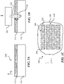
- FIG. 1A and FIG. 1B present a side cross-sectional view of a substrate 100, at different stages during formation of a mesa device structure 140, according to various embodiments of the disclosure.
- FIG. 1C presents a top plan view of the substrate 100, at the stage of formation as indicated in FIG. 1B .
- the substrate 100 is shown including an inner region 110, having a first polarity.
- the substrate 100 may be a N-type substrate, where the inner region 110 is also n-type.
- a surface layer 112 is disposed on the inner region 110.
- the surface layer 112 comprises a second polarity, opposite the first polarity of the inner region 110.
- the surface layer 112 may be a P-type layer.
- the surface layer 112 may be formed using any suitable known method.
- the thickness and dopant concentration in surface layer 112 may be selected according to the type of device to be formed from the mesa device structure 140.
- a suitable dopant concentration may be chose to generate a target breakdown voltage, such as 15 V-20 V, or 30 V-35 V, according to different non-limiting embodiments.
- the thickness of the surface layer 112 may be chose to generate the desired electrical properties of a device to be formed. In some non-limiting embodiments the thickness of the surface layer 112 may be in the range of two mils.
- FIG. 1B there is shown a novel operation for forming a mesa device structure, in accordance with embodiments of the disclosure.
- a saw apparatus 120 is employed to form a trench region 130 in a surface region of the substrate 100.
- the saw apparatus 120 may be a known type of saw, and may, for example, employ a cutting blade 122, formed of a metal, ceramic, carbide, diamond, or combination thereof, according to non-limiting embodiments of the disclosure.
- the saw apparatus 120 may be arranged to generate a trench having a controllable and fixed depth within the substrate 100.
- the formation of the trench region 130 may be used to electrically isolate a portion of the surface layer 112, in order to form a semiconductor device.
- the trench region 130 is defined by a trench depth d, wherein the trench depth d is at least as great as a thickness of the surface layer 112.
- the trench depth d may be at least two mils, while the trench width w may be on the order of several mils, such as five mils, 10 mils, or 20 mils. The embodiments are not limited in this context.
- the saw apparatus 120 may be arranged to generate a two-dimensional pattern for the trench region 130, such as a grid pattern.
- a two-dimensional pattern for the trench region 130 such as a grid pattern.
- FIG. 1C an array of mesa device structures 140 are shown, where these device structures form a grid of rectangular mesas, each mesa being surrounded by the trench region 130 that forms a perimeter around the given mesa device structure.
- the trench region 130 extends at least through an entirety of the surface layer 112
- the surface layer 112 within a given mesa device structure is electrically isolated from the portion of the surface layer 112 within any other mesa device structure, since current must travel through the inner region 110, of opposite polarity.
- the trench region 130 may be formed by generating a series of saw cuts along the X-axis, and a series of saw cuts along the Y-axis, to form a grid pattern, as shown.
- mesa isolation may be accomplished essentially in one operation, involving a saw cutting process that can be programmed to generate a repeatable trench depth suitable for a given device formation.
- FIG. 2A and FIG. 2B present a side cross-sectional view of a substrate 200, at different stages during formation of a mesa device structure 240, according to various embodiments of the disclosure.
- the substrate 200 is shown including an inner region , the semiconductor substrate comprising an inner region 210, having a first polarity.
- the substrate 200 may be a N-type substrate, where the inner region 210 is also n-type.
- the substrate 200 may be a P-type substrate, where the inner region 210 is also p-type.
- a first surface layer 212 is disposed on the inner region 210.
- the first surface layer 212 comprises a second polarity, opposite the first polarity of the inner region 210.
- the first surface layer 212 may be a P-type layer.
- the first surface layer 212 may be formed using any suitable known method.
- the thickness and dopant concentration in first surface layer 212 may be selected according to the type of device to be formed from the mesa device structure 240.
- the substrate 200 includes a second surface layer 216, disposed on an opposite side of the inner region 210, where the second surface layer 216 comprises a second polarity, opposite the first polarity of the inner region 210.
- the substrate 200 further includes a first oxide layer 214, disposed over the first surface layer 212, and a second oxide layer 218, disposed over the second surface layer 216.
- the substrate 200 may function as a bi-directional diode.
- the first surface layer 212 and the second surface layer 216 may have a same thickness and a same dopant concentration as one another, while in other embodiments the thickness and/or dopant concentration of the first surface layer 212 and second surface layer 216 may differ.
- the first surface layer 212 and second surface layer 216, as well as the first oxide layer 214 and second oxide layer 218 may be formed in a single diffusion process to establish base junctions.
- the thickness and dopant concentration of the first surface layer 212 may be chosen according to the device application of a mesa device structure to be formed.
- a saw apparatus 220 is employed to form a trench region 230 in a surface region of the substrate 100.
- the saw apparatus 220 may be a known type of saw, and may, for example, employ a cutting blade (not shown), formed of a metal, ceramic, carbide, diamond, or combination thereof, according to non-limiting embodiments of the disclosure.
- the saw apparatus 220 may be arranged to generate a trench having a controllable and fixed depth within the substrate 200.
- the formation of the trench region 230 may be used to electrically isolate a portion of the first surface layer 212, in order to form a semiconductor device.
- the trench region 230 is defined by a trench depth d, as shown in FIG. 2B , wherein the trench depth d is at least as great as a thickness of the first surface layer 212.
- the trench depth d may be at least two mils, while the trench width w may be on the order of several mils, such as five mils, 10 mils, or 20 mils. The embodiments are not limited in this context.
- the saw apparatus 220 may be arranged to generate a two-dimensional pattern for the trench region 230, such as a grid pattern, as generally described with respect to FIG. 1C .
- the trench region 230 has been defined by a saw cut, while debris 232, formed as a byproduct of the saw cut, may remain in the trench region 230, as well as in other surface regions of the substrate 200.
- the cleaning operation may be accomplished using a chemical process 234, shown schematically by the arrows.
- the chemical process 234 is an MAE etch (a formula for the MAE etch may be represented by a 2:1:1 mixture of (HF:HNO 3 :CH 3 COOH), wherein the MAE etch removes residual semiconductor debris and ion contamination in a surface of the trench region 230.
- further operations may include the formation of a passivation layer in the trench region 230.
- An advantage of the embodiment of FIGs. 2A, 2B is that formation of a mesa device structure merely entails a saw cutting operation, followed by a simple chemical etch process.
- the mesa device structure 240 may be formed on both sides of the substrate.
- a mesa device structure 240 may be formed both on the upper surface 202 of substrate 200, while a mesa device structure 240 is also formed (using second surface layer 216) on the lower surface 204 of substrate 200.
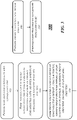
- FIG. 3 depicts a process flow 300, according to embodiments of the disclosure.
- a semiconductor substrate is provided, such as a silicon substrate.
- the semiconductor substrate may be doped as first conductivity type (first polarity) and at a suitable doping concentration for forming a device, such as a breakdown diode.
- the semiconductor substrate may be doped to have an N-type polarity.
- a surface layer of a second conductivity type is formed in a surface region on one main surface of the semiconductor substrate, where the surface layer and an inner portion of the semiconductor substrate define a p/n junction.
- the surface layer may be formed on the semiconductor substrate to define a P-type semiconductor layer that is disposed now over an N-type inner portion of the semiconductor substrate.
- a second surface layer of the second conductivity type may be formed on an opposite main surface of the semiconductor substrate.
- a second p/n junction may be formed between the inner portion of the semiconductor substrate and the second surface layer.
- a trench structure is formed in a surface region of the semiconductor substrate, using a saw cut process, where the trench structure extends at least to the depth of the p/n junction. and wherein trench structure encloses at least one mesa structure.
- the saw cut process may be performed in a manner that the trench structure forms a two-dimensional perimeter that defines at least one mesa structure.
- the saw cut process may define a two-dimensional rectangular grid that defines an array of mesa structures.
- a chemical etch process is performed, subsequently to the saw cut process, to remove debris and clean the trench structure.
- the chemical etch process may be any suitable etch process as known in the art, such as an MAE process.
- a passivation process is performed to passivate the trench structure.
- FIG. 4 depicts another exemplary process flow 400.
- a semiconductor substrate of a first conductivity type is provided.
- a first surface layer of second conductivity type is formed in a first surface of the semiconductor substrate, and a second surface layer of the second conductivity type is formed in a second surface of the semiconductor substrate.
- the first semiconductor layer and an inner portion of the semiconductor substrate define a first p/n junction
- the second semiconductor layer and inner portion of the semiconductor substrate define a second p/n junction.
- a first trench structure is formed in the first surface of the semiconductor substrate, using a saw process, wherein the first trench structure extends at least to depth of the first p/n junction, and wherein the first trench structure encloses at least one mesa structure on the first surface.
- a second trench structure is formed in the second surface of the semiconductor substrate, using the saw process, wherein the second trench structure extends at least to depth of the second p/n junction, and wherein the second trench structure encloses at least one additional mesa structure on the second surface.
- a chemical etch is performed to clean the first trench structure and the second trench structure.
- the chemical etch may be any suitable etch process as known in the art, such as an MAE process.
- a passivation process is performed to passivate the first trench structure and the second trench structure.
- a bi-directional diode device may be formed with mesa device structures on both sides of the semiconductor substrate.
Landscapes
- Element Separation (AREA)
- Weting (AREA)
- Bipolar Transistors (AREA)
Applications Claiming Priority (1)
| Application Number | Priority Date | Filing Date | Title |
|---|---|---|---|
| CN202110335748.7A CN115148589B (zh) | 2021-03-29 | 2021-03-29 | 半导体台面器件形成方法 |
Publications (1)
| Publication Number | Publication Date |
|---|---|
| EP4068338A1 true EP4068338A1 (fr) | 2022-10-05 |
Family
ID=80979134
Family Applications (1)
| Application Number | Title | Priority Date | Filing Date |
|---|---|---|---|
| EP22164762.1A Pending EP4068338A1 (fr) | 2021-03-29 | 2022-03-28 | Procédé de formation de dispositif mesa à semi-conducteur |
Country Status (5)
| Country | Link |
|---|---|
| US (1) | US20220310821A1 (fr) |
| EP (1) | EP4068338A1 (fr) |
| KR (1) | KR20220135211A (fr) |
| CN (1) | CN115148589B (fr) |
| TW (1) | TWI881212B (fr) |
Citations (3)
| Publication number | Priority date | Publication date | Assignee | Title |
|---|---|---|---|---|
| JPS5760843A (en) * | 1980-09-29 | 1982-04-13 | Nec Corp | Manufacture of semiconductor device |
| EP0948036A2 (fr) * | 1998-03-30 | 1999-10-06 | GENERAL SEMICONDUCTOR, Inc. | Méthode de formation par sciage de puces semi-conductrices à structure mésa |
| EP3113219A1 (fr) * | 2015-06-30 | 2017-01-04 | SEMIKRON Elektronik GmbH & Co. KG | Composant semi-conducteur et procede de sa fabrication |
Family Cites Families (29)
| Publication number | Priority date | Publication date | Assignee | Title |
|---|---|---|---|---|
| US3152939A (en) * | 1960-08-12 | 1964-10-13 | Westinghouse Electric Corp | Process for preparing semiconductor members |
| US3535774A (en) * | 1968-07-09 | 1970-10-27 | Rca Corp | Method of fabricating semiconductor devices |
| US3555372A (en) * | 1969-01-02 | 1971-01-12 | Jearld L Hutson | Semiconductor bilateral switching device |
| US3608186A (en) * | 1969-10-30 | 1971-09-28 | Jearld L Hutson | Semiconductor device manufacture with junction passivation |
| US3735483A (en) * | 1970-03-20 | 1973-05-29 | Gen Electric | Semiconductor passivating process |
| JPS4974486A (fr) * | 1972-11-17 | 1974-07-18 | ||
| US3852876A (en) * | 1973-01-02 | 1974-12-10 | Gen Electric | High voltage power transistor and method for making |
| US3972113A (en) * | 1973-05-14 | 1976-08-03 | Mitsubishi Denki Kabushiki Kaisha | Process of producing semiconductor devices |
| US4063272A (en) * | 1975-11-26 | 1977-12-13 | General Electric Company | Semiconductor device and method of manufacture thereof |
| US4148672A (en) * | 1976-02-02 | 1979-04-10 | General Electric Company | Glass passivated gold diffused rectifier pellet and method for making |
| JPS584814B2 (ja) * | 1976-04-27 | 1983-01-27 | 三菱電機株式会社 | 半導体装置 |
| DE2730130C2 (de) * | 1976-09-14 | 1987-11-12 | Mitsubishi Denki K.K., Tokyo | Verfahren zum Herstellen von Halbleiterbauelementen |
| DE2751485A1 (de) * | 1977-11-18 | 1979-05-23 | Semikron Gleichrichterbau | Verfahren zum herstellen von halbleiterkoerpern mit definiertem, durch aetzen erzielten und mit einem glas abgedeckten randprofil |
| US4551353A (en) * | 1981-12-30 | 1985-11-05 | Unitrode Corporation | Method for reducing leakage currents in semiconductor devices |
| HUT73312A (en) * | 1992-09-14 | 1996-07-29 | Badehi | Method and apparatus for producing integrated circuit devices, and integrated circuit device |
| FR2709872B1 (fr) * | 1993-09-07 | 1995-11-24 | Sgs Thomson Microelectronics | Diode de shockley bidirectionnelle. |
| DE19601261C1 (de) * | 1996-01-16 | 1997-04-10 | Itt Ind Gmbh Deutsche | Verfahren und Hilfsvorrichtung zum Herstellen von Halbleiterschaltungselementen |
| US6555447B2 (en) * | 1999-06-08 | 2003-04-29 | Kulicke & Soffa Investments, Inc. | Method for laser scribing of wafers |
| US6448589B1 (en) * | 2000-05-19 | 2002-09-10 | Teccor Electronics, L.P. | Single side contacts for a semiconductor device |
| JP2002184952A (ja) * | 2000-12-15 | 2002-06-28 | Shindengen Electric Mfg Co Ltd | 半導体装置、半導体装置の製造方法 |
| US20060216913A1 (en) * | 2005-03-25 | 2006-09-28 | Pu-Ju Kung | Asymmetric bidirectional transient voltage suppressor and method of forming same |
| FR2969825B1 (fr) * | 2010-12-23 | 2013-07-12 | St Microelectronics Tours Sas | Composant vertical bidirectionnel a double sillonnage |
| FR2969824B1 (fr) * | 2010-12-23 | 2013-09-20 | St Microelectronics Tours Sas | Diode de shockley bidirectionnelle a mesa prolonge |
| FR2969823B1 (fr) * | 2010-12-23 | 2013-09-20 | St Microelectronics Tours Sas | Diode de shockley bidirectionnelle de type mesa |
| JP6004561B2 (ja) * | 2012-03-30 | 2016-10-12 | 国立研究開発法人産業技術総合研究所 | 炭化珪素半導体素子の製造方法 |
| CN104091823A (zh) * | 2014-07-24 | 2014-10-08 | 江苏捷捷微电子股份有限公司 | 一种瞬态抑制二极管芯片及其制造方法 |
| WO2016159962A1 (fr) * | 2015-03-31 | 2016-10-06 | Vishay General Semiconductor Llc | Limiteur de surtension (tvs) bidirectionnel mince ou diode zener |
| TWI724685B (zh) * | 2019-03-01 | 2021-04-11 | 美商Ipower半導體公司 | 遮蔽閘極溝槽式金氧半導體場效電晶體元件 |
| CN112928168B (zh) * | 2019-12-06 | 2025-06-27 | 力特半导体(无锡)有限公司 | 具有不对称击穿电压的tvs二极管和组件 |
-
2021
- 2021-03-29 CN CN202110335748.7A patent/CN115148589B/zh active Active
-
2022
- 2022-03-28 EP EP22164762.1A patent/EP4068338A1/fr active Pending
- 2022-03-28 US US17/706,008 patent/US20220310821A1/en active Pending
- 2022-03-29 TW TW111111892A patent/TWI881212B/zh active
- 2022-03-29 KR KR1020220039080A patent/KR20220135211A/ko not_active Ceased
Patent Citations (3)
| Publication number | Priority date | Publication date | Assignee | Title |
|---|---|---|---|---|
| JPS5760843A (en) * | 1980-09-29 | 1982-04-13 | Nec Corp | Manufacture of semiconductor device |
| EP0948036A2 (fr) * | 1998-03-30 | 1999-10-06 | GENERAL SEMICONDUCTOR, Inc. | Méthode de formation par sciage de puces semi-conductrices à structure mésa |
| EP3113219A1 (fr) * | 2015-06-30 | 2017-01-04 | SEMIKRON Elektronik GmbH & Co. KG | Composant semi-conducteur et procede de sa fabrication |
Also Published As
| Publication number | Publication date |
|---|---|
| TWI881212B (zh) | 2025-04-21 |
| TW202245032A (zh) | 2022-11-16 |
| CN115148589A (zh) | 2022-10-04 |
| CN115148589B (zh) | 2025-08-29 |
| KR20220135211A (ko) | 2022-10-06 |
| US20220310821A1 (en) | 2022-09-29 |
Similar Documents
| Publication | Publication Date | Title |
|---|---|---|
| US9455316B2 (en) | Three-dimensional electrostatic discharge semiconductor device | |
| CN101499421B (zh) | 台型半导体装置及其制造方法 | |
| KR101955055B1 (ko) | 전력용 반도체 소자 및 그 소자의 제조 방법 | |
| CN102326256A (zh) | 用于改进沟槽屏蔽式半导体装置和肖特基势垒整流器装置的结构和方法 | |
| JPH0210576B2 (fr) | ||
| US20090224354A1 (en) | Junction barrier schottky diode with submicron channels | |
| CN116364644A (zh) | 用于形成薄的绝缘体上半导体soi衬底的方法 | |
| US10685883B1 (en) | Method of wafer dicing and die | |
| JP5509543B2 (ja) | 半導体装置の製造方法 | |
| US5541140A (en) | Semiconductor arrangement and method for its manufacture | |
| KR102050551B1 (ko) | 계단 구조의 트렌치를 구비한 파워 반도체 및 그 제조 방법 | |
| JP2019046834A (ja) | 半導体装置の製造方法 | |
| CN110265358A (zh) | 半导体器件沟道的制作方法、半导体器件及其制造方法 | |
| US20230178377A1 (en) | Method of manufacturing semiconductor device and semiconductor device | |
| EP4068338A1 (fr) | Procédé de formation de dispositif mesa à semi-conducteur | |
| US12543379B2 (en) | Integrated circuit structure in porous semiconductor region and method to form same | |
| US20140151841A1 (en) | Semiconductor devices having a positive-bevel termination or a negative-bevel termination and their manufacture | |
| CN109643686B (zh) | 具有侧面扩散的沟槽插塞的半导体器件 | |
| SE519628C2 (sv) | Tillverkningsförfarande för halvledarkomponent med deponering av selektivt utformat material,vilket är ogenomträngligt för dopjoner | |
| CN113497135A (zh) | 反向传导绝缘栅双极晶体管的制造方法 | |
| JP6861914B1 (ja) | 半導体装置及び半導体装置の製造方法 | |
| KR101415599B1 (ko) | Pn 접합 다이오드 제조방법 | |
| CN111128885A (zh) | 半导体装置和其形成方法 | |
| CN101901840B (zh) | 肖特基二极管装置及其制造方法 | |
| CN107622972B (zh) | 用于加工晶片的方法和层堆叠 |
Legal Events
| Date | Code | Title | Description |
|---|---|---|---|
| PUAI | Public reference made under article 153(3) epc to a published international application that has entered the european phase |
Free format text: ORIGINAL CODE: 0009012 |
|
| STAA | Information on the status of an ep patent application or granted ep patent |
Free format text: STATUS: THE APPLICATION HAS BEEN PUBLISHED |
|
| AK | Designated contracting states |
Kind code of ref document: A1 Designated state(s): AL AT BE BG CH CY CZ DE DK EE ES FI FR GB GR HR HU IE IS IT LI LT LU LV MC MK MT NL NO PL PT RO RS SE SI SK SM TR |
|
| STAA | Information on the status of an ep patent application or granted ep patent |
Free format text: STATUS: REQUEST FOR EXAMINATION WAS MADE |
|
| 17P | Request for examination filed |
Effective date: 20230330 |
|
| RBV | Designated contracting states (corrected) |
Designated state(s): AL AT BE BG CH CY CZ DE DK EE ES FI FR GB GR HR HU IE IS IT LI LT LU LV MC MK MT NL NO PL PT RO RS SE SI SK SM TR |