EP0948036A2 - Méthode de formation par sciage de puces semi-conductrices à structure mésa - Google Patents
Méthode de formation par sciage de puces semi-conductrices à structure mésa Download PDFInfo
- Publication number
- EP0948036A2 EP0948036A2 EP99300936A EP99300936A EP0948036A2 EP 0948036 A2 EP0948036 A2 EP 0948036A2 EP 99300936 A EP99300936 A EP 99300936A EP 99300936 A EP99300936 A EP 99300936A EP 0948036 A2 EP0948036 A2 EP 0948036A2
- Authority
- EP
- European Patent Office
- Prior art keywords
- wafer
- layer
- mesa
- junction
- grooves
- Prior art date
- Legal status (The legal status is an assumption and is not a legal conclusion. Google has not performed a legal analysis and makes no representation as to the accuracy of the status listed.)
- Withdrawn
Links
Images


Classifications
-
- H—ELECTRICITY
- H10—SEMICONDUCTOR DEVICES; ELECTRIC SOLID-STATE DEVICES NOT OTHERWISE PROVIDED FOR
- H10W—GENERIC PACKAGES, INTERCONNECTIONS, CONNECTORS OR OTHER CONSTRUCTIONAL DETAILS OF DEVICES COVERED BY CLASS H10
- H10W20/00—Interconnections in chips, wafers or substrates
- H10W20/01—Manufacture or treatment
-
- H—ELECTRICITY
- H10—SEMICONDUCTOR DEVICES; ELECTRIC SOLID-STATE DEVICES NOT OTHERWISE PROVIDED FOR
- H10P—GENERIC PROCESSES OR APPARATUS FOR THE MANUFACTURE OR TREATMENT OF DEVICES COVERED BY CLASS H10
- H10P52/00—Grinding, lapping or polishing of wafers, substrates or parts of devices
Definitions
- This invention relates to semiconductor chips having a mesa structure, and particularly to the manufacture of such chips using a mechanical sawing process.
- Such anisotropical etching processes comprise providing a silicon wafer coated with a masking layer of silicon nitride, applying a photoresist layer over the masking layer, and forming a mesa defining pattern in the photoresist using a photomask. Etching is then performed through the patterned photoresist layer and into the underlying masking layer and wafer for defining a plurality of mesas on the wafer surface. Having defined the mesas, subsequent processing steps can be performed for further defining the parameters of each mesa containing chip to be formed. Then, the mesa side walls are oxidized for passivating the mesa wall surfaces.
- the masking layers overlying the mesas are removed (typically in a photolithographic process using a photomask) for exposing silicon surfaces at the mesa tops, the exposed surfaces and wafer bottom surface are metal plated for forming chip electrodes, and the thus basically completed chip structures are separated in a wafer-dicing operation, e.g., by mechanical sawing.
- a silicon semiconductor wafer substantially completely processed and including metal electrodes on opposite major surfaces, is adhered, via a wax layer, to a rigid support substrate.
- a plurality of orthogonal grooves having sloped side surfaces are then sawed entirely through the thickness of the wafer and partly into the underlying wax layer.
- An etching process is used to smooth the groove sawed surfaces, and a silicon resin is then deposited onto the grooved surface of the wafer for filling in the grooves.
- the resin after curing, adheres strongly to the groove walls but only poorly to the metal plated surface of the wafer.
- the resin is then readily removed, as by buffing, from the wafer plated surface without removal of the resin from within the grooves.
- the wafer is then separated from the supporting substrate. Although the wafer has been sawed through into separate chips, the chips remain attached to one another by the cured resin between and attached to the chips. Solder is then selectively applied to the surfaces of the metal electrodes on the chips, and the chips are finally separated by slicing through the resin layers between the chips. The side surfaces of the chips remain coated with the cured resin which serves to passivate the chip sides.
- the Shyr process is basically a variation on known wafer dicing processes typically performed after all the basic processing of the precursor chips has been completed. Specifically, at the stage of wafer production when the Shyr dicing process is performed, all high temperature processing of the precursor chips has been completed and further high temperature processing is avoided.
- the metal electrodes preferably provided in a high temperature processing step, i.e., in excess of 400°C
- the chip passivating material used i.e., the disclosed silicone resin, is applied and cured at lower temperatures, e.g., around 200°C.
- the present invention involves the use of mechanical sawing as a direct substitution for the previously used anisotropic etching process and at a relatively early part of the chip fabrication schedule. None in Shyr shows nor suggests such direct substitution or how it could be accomplished.
- a method of making semiconductor chips comprises providing a semiconductor wafer of known type heretofore used for fabricating chips having mesa structures.
- the wafer includes a p-n junction lying in a surface parallel to major surfaces of the wafer, and the upper surface of the semiconductor material of the wafer is covered with a masking layer, preferably of silicon nitride.
- Spaced apart mesas are then formed in an upper portion of the wafer by sawing a plurality of intersecting grooves into the wafer through the masking layer.
- the sawed grooves have sloped walls and have a depth (which can be reached after a subsequent etching process for smoothing the sawed surfaces of the wafer) for intersecting and exposing edges of the junctions at the mesa side walls.
- a passivating material preferably glass
- the masking layers of silicon nitride at the top of each mesa protect the underlying semiconductor material against oxidation and against contacting by the passivation glass.
- the masking layers are then removed (by etching, and without use of a photomask) for exposing the underlying mesa semiconductor material.
- the thus exposed mesa top surfaces and the bottom of the wafer are then metalized to substantially complete the processing of the wafer which is then diced into separate mesa containing chips, e.g., by mechanical sawing.
- a support structure e.g., a sheet of adhesive tape 12.
- the tape 12 serves to support the wafer while it is being grooved by sawing, as shortly described.
- the sawing of wafers typically for dicing them, and the use of tapes in the sawing process, are known.
- the wafer 10 can be identical to known wafers used for fabricating chips for use in semiconductor devices such as discrete rectifiers, TVS S (transient voltage suppressors), transistors, certain types of thyristors, and the like.
- semiconductor devices such as discrete rectifiers, TVS S (transient voltage suppressors), transistors, certain types of thyristors, and the like.
- the wafer 10 in this embodiment, includes a bottom p + layer 14 forming a planar p-n junction 16 with an overlying n - layer 18 overlaid, in turn, with an n + layer 20.
- planar junction is simply meant a junction lying in a plane; the term “planar” not referring to the known “planar junction process."
- the bottom layer 14 can be formed as a discrete substrate, and the layers 18 and 20 sequentially epitaxially grown thereon.
- the top layer 20 can be formed by diffusion of n-type dopants into the epitaxially grown n - layer 18.
- an n - discrete layer 18 substrate can be n-doped through one side to form the upper n + layer 20 and p-doped through the other side to form the bottom p + layer 14.
- the upper surface 24 of the layer 20 (forming the upper surface of the silicon wafer 10) is covered with a masking layer 22.
- the masking layer is used, as hereinafter described, for allowing localized etching and high temperature processing of the wafer and for preventing contamination of the top surfaces of the layers 20 in the mesas to be formed.
- a preferred material for the layer 22 is silicon nitride, at least partially because silicon nitride is selectively etchable relative to glass passivating layers later provided. The use of silicon nitride masking layers in the fabrication of semiconductor devices is known.
- a plurality of orthogonal grooves 28 are provided in the upper portion of the wafer.
- the grooves 28 do not extend entirely through the wafer 10 but sub-divide the wafer into a plurality of identical mesas 34 (only one complete mesa being shown in Figs. 2 and 3) extending upwardly from a common underlying substrate 14.
- the mesas 34 have a square cross-sectional shape increasing in area from the top surface 30 of the silicon nitride layer 22 at the top of each mesa downwardly to the substrate 14.
- the mesa side walls 36 are straight and uniformly sloped.
- Each mesa includes a portion of the planar p-n junction 16 originally present in the wafer 10, and the edges 16a of each mesa junction are exposed at the mesa side walls 36.
- the intersections of the mesa p-n junctions with the mesa sloped walls provide a desired voltage breakdown characteristic of the semiconductor chips.
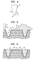
- the orthogonal grooves 28 in the wafer 10 are provided by sawing using, for example, a disc saw 38 (Fig. 4) having a diamond blade.
- the cutting edge of the blade is beveled at a preselected angle ⁇ and the blade sloped sides 40 are joined by a flat side 42.
- the grooves 28 (Fig. 2) sawed into the wafer 10 correspond in shape exactly to that of the blade edge.
- the sawing of silicon wafers typically, as earlier noted, for wafer dicing
- diamond blades having selected shapes and dimensions are commercially available on a customized basis.
- the blade bevel angle ⁇ (and the corresponding groove wall bevel angle ⁇ ) is between 30-75 degrees.
- blades having curved side walls can be used to provide grooves having curved walls.
- the selection of the desired groove wall slope and shape is in accordance with known technology and is dependent upon the material used for passivation and the ratings of the particular semiconductor devices later to incorporate chips made according to the present invention.
- each wafer 10 Although a relatively large number of grooves 28 are sawed into each wafer 10 (e.g., 40 by 40 grooves in a 100 mm diameter wafer), it is found preferable to make but one cut at a time using a single blade. Plural cuts can be simultaneously made using ganged blades but, generally, excessive dimensional variations result.
- the planar p-n junction 16 within each mesa 34 must intersect the mesa walls 36.
- the mesa forming grooves 28 thus must be deep enough to intersect the planar p-n junction 16 present in the starting wafer 10, and must extend slightly below the exposed p-n junction edges 16a.
- the groove depth beyond the p-n junction 16 must be at least comparable to the maximum width of the depletion region spreading downwardly from the p-n junction 16 at voltage breakdown conditions. Because of the relatively high conductivity of the p + layer 14, only a relatively small spreading of the depletion region occurs within the layer 14.
- the depth of the grooves 28 need be only slightly greater than the depth of the p-n junction 16 within each mesa. Such depth is a function of the particular semiconductor device to be made.
- the p-n junction 16 (of the wafer shown in Fig. 1) is from 4-7 mils beneath the wafer top surface 30, and the depth of the grooves, as initially formed by sawing, is about equal to the depth of the p-n junction 16.
- the final depth of the grooves (as illustrated in Fig. 2) is determined by an etching process next performed to smoothen the groove walls formed in the sawing process.
- Etch smoothing of silicon surfaces is known and described, for example, in the afore-cited patent to Shyr.
- the preferred etching solution comprises nitric, acetic and hydrofluoric acids in the ratio of 3:1:1.
- the etching is performed at a temperature of 8-12°C with an immersion time of around 30-60 seconds.
- the grooves 28 are sawed to a depth of 4.5 mils, and reach a final depth (Fig. 2) of 5 mils after etching.
- Fig. 2 shows the wafer 10 after the etching step.
- the tape 12 shown in Fig. 1 is present during sawing of the wafer but is removed prior to the etching.
- the edge 16a of the p-n junction 16 in each mesa 34 is exposed at the mesa side wall 36, and it is necessary that the mesa side walls 36 be encased within a suitable "passivating" material.
- passivating layers are well known in semiconductor devices, and, typically, silicon dioxide passivating layers are thermally grown on the mesa walls.
- a passivating material is selected for the purpose, as hereinafter described, of avoiding the need for the use of photomasks in subsequent processes to be performed.
- the passivating material used is a relatively thick (as hereinafter discussed) layer of a known glass typically used for encapsulation purposes in semiconductor devices, e.g., a zinc (or lead)-boro-silicate glass.
- a slurry 46 Fig. 5
- doctor bladed e.g., by a squeegee 47
- Other methods for applying the glass layer to the workpiece comprise electrophoresis and screen printing.
- electrophoresis the glass is selectively deposited only on electrically conductive surfaces; thus only on the silicon mesa side surfaces 36, and not on the silicon nitride layers 22 covering the mesa tops.
- the glass slurry 46 substantially fills the grooves 28. Then, the glass is vitrified into a smooth encapsulating layer by a known firing process, e.g., slowly heating the workpiece to a temperature around 830°C, where melting and flowing occurs, followed by an even slower cooling of the glass layer for annealing the glass.
- a known firing process e.g., slowly heating the workpiece to a temperature around 830°C, where melting and flowing occurs, followed by an even slower cooling of the glass layer for annealing the glass.
- the vitrified glass layer 46a is shown in Fig. 7.
- the vitrified glass is compacted and hermetically encapsulates the mesa side walls 36.
- the thickness of the glass layer 46a varies, as shown, but the minimum thickness of the layer 46a (excluding edge regions close to the mesa top surfaces 24) is around 50,000 Angstroms, which is significantly greater than the thickness, e.g., around 2,000 Angstroms, of the layer 22 of silicon nitride on each mesa. (Also, the minimum glass layer thickness is significantly greater than that of any other optional layers of passivating materials (described hereinafter) non-selectively deposited onto the wafer.)
- glass is a preferred passivating material (superior, for example, to the silicone resin passivating material used in the process disclosed in the afore-cited Shyr patent), and that proper application of the glass includes heating the workpiece to the afore-described 830°C.
- Such heating of the workpiece is made practical by the presence of the silicon nitride layers 22 which, during the glass firing, prevent contamination or oxidation of the top surfaces 24 of the n + silicon layer 20 overlaid by the silicon nitride layers 22.
- the passivation material thus comprises a layer 25 (shown in Fig. 5 by way of example but not in other figures) of silicon dioxide (having a thickness, not critical, e.g., from 5,000-20,000 Angstroms) covered by a layer of glass. Also, and again prior to the glassing, additional dopants can be added to and diffused within the mesas.
- a layer 25a (shown in Fig. 6 by way of example but not in other figures) of silicon dioxide can be directly deposited onto the entire grooved surface of the wafer by the known "low temperature oxide” process; or, in similar known deposition processes, deposited at relatively high temperatures.
- the deposited oxide layer serves to passivate the silicon side walls 36 of the mesas either directly or in combination with a previously provided passivating material, e.g., the afore-described thermally grown oxide.
- the deposited oxide also covers the silicon nitride layers 22 on the mesa tops, but the layers 22 prevent contact of the deposited oxide layer with the silicon surfaces 24 of the mesas underlying the nitride layers 22.
- passivating materials are polycrystalline silicon and silicon nitride. Techniques for depositing these materials onto a substrate are known.
- the glass layer 46a (Fig. 7) is then provided in a process leaving the mesa tops not covered by the glass layer.
- a passivating material layer e.g., the deposited materials silicon dioxide, polycrystalline silicon and/or silicon nitride
- such deposited passivating material remains exposed on top of the silicon nitride layers 22. Because these materials are later to be removed, along with the silicon nitride layers 22 (as now to be described), it is preferred that any such deposited layers be relatively thin, e.g., around 300-500 Angstroms, in comparison to the much thicker layer 46a of glass (e.g., having the aforementioned minimum thickness of around 50,000 Angstroms).
- the silicon nitride layers 22, and any covering layers are removed. If the silicon nitride layers 22 are not covered, the layers 22 can be removed in a silicon nitride selective etchant such as phosphoric acid which only weakly etches silicon dioxide and glass.
- a silicon nitride selective etchant such as phosphoric acid which only weakly etches silicon dioxide and glass.
- a preferred process for removing the silicon nitride layers 22 including any layers thereon is a plasma etching process which effectively removes all the exposed surface materials (i.e., the glass layer 46a, the silicon nitride layers 22 and/or the optionally deposited silicon dioxide, polycrystalline silicon and silicon nitride passivating layers) but at a carefully controlled rate.
- the plasma etching process when the mesa covering silicon nitride layers 22 are just removed (along with any covering deposited layers), along with an equal thickness of the glass layer 46a, the process is immediately stopped (making use of known plasma composition monitoring).
- the glass layer minimum thickness is significantly greater than the thickness of the removed silicon nitride layers (plus any covering deposited passivating layers), the remaining thickness of the glass layers 46a (plus any underlying passivating layers) is still adequate for effective passivation of the mesa sloped walls.
- Fig. 8 shows the wafer 10 without the silicon nitride layers 22.
- the wafer With the removal of the silicon nitride layers 22 and the exposure of the n + layers 20, which now form the mesa tops, the wafer is basically ready for metalization. That is, because the silicon nitride layers 22 prevented oxidation or other contamination of the upper surfaces 24 of the silicon layers 20, upon removal of the silicon nitride layers 22, as described, the uncovered silicon surfaces 24 are sufficiently clean (after a brief dip in a weak HF etchant to remove any "native oxide" on the surfaces 24) for the performance of the metalizing process.
- the glass layers 46a within the grooves 28 are electrically non-conductive, and using known electroless processes, various layers 50 (Fig.
- metal e.g., of nickel and gold
- metal e.g., of nickel and gold
- FIG. 8 A portion of the thus completed wafer is shown in Fig. 8. Individual chips 10a, each for inclusion in a discrete semiconductor device, are obtained by dicing the wafer, as by sawing vertically through the grooves 28 along the dash line 52 shown in Fig. 8. Although the glass layers 46a surrounding each mesa 34 are thus sliced through, the glass layers do not crack but remain firmly adhered to the mesa side walls.
- the separated chips 10a are substantially identical to chips having mesas formed by known etching processes.
- further processing of the chips for eventual fabrication of semiconductor devices can be in accordance with known procedures which are not herein described.
- a significant advantage of the invention is that semiconductor wafers can be processed into devices entirely without the need for photolithographic processes, i.e., without the need for photoresist layers and corresponding photomasks for patterning first the photoresist layers followed by selective etching through the patterned layers.
- the various mesas are formed by mechanical sawing (followed, for smoothening and deepening functions, by an etching process not attacking the mesa silicon top surface 24 owing to the covering layers 22 of silicon nitride), and the steps of readying the mesa silicon surfaces for, and metal plating the mesa silicon surfaces, are likewise performed by "selective" processes not requiring photolithographic processes.
Landscapes
- Dicing (AREA)
- Thyristors (AREA)
- Mechanical Treatment Of Semiconductor (AREA)
- Bipolar Transistors (AREA)
- Weting (AREA)
Applications Claiming Priority (2)
| Application Number | Priority Date | Filing Date | Title |
|---|---|---|---|
| US09/050,106 US5882986A (en) | 1998-03-30 | 1998-03-30 | Semiconductor chips having a mesa structure provided by sawing |
| US50106 | 1998-03-30 |
Publications (2)
| Publication Number | Publication Date |
|---|---|
| EP0948036A2 true EP0948036A2 (fr) | 1999-10-06 |
| EP0948036A3 EP0948036A3 (fr) | 2002-03-20 |
Family
ID=21963407
Family Applications (1)
| Application Number | Title | Priority Date | Filing Date |
|---|---|---|---|
| EP99300936A Withdrawn EP0948036A3 (fr) | 1998-03-30 | 1999-02-09 | Méthode de formation par sciage de puces semi-conductrices à structure mésa |
Country Status (6)
| Country | Link |
|---|---|
| US (1) | US5882986A (fr) |
| EP (1) | EP0948036A3 (fr) |
| JP (1) | JP4841021B2 (fr) |
| KR (1) | KR100298063B1 (fr) |
| CN (1) | CN1134827C (fr) |
| TW (1) | TW417190B (fr) |
Cited By (1)
| Publication number | Priority date | Publication date | Assignee | Title |
|---|---|---|---|---|
| EP4068338A1 (fr) * | 2021-03-29 | 2022-10-05 | Littelfuse Semiconductor (Wuxi) Co., Ltd. | Procédé de formation de dispositif mesa à semi-conducteur |
Families Citing this family (30)
| Publication number | Priority date | Publication date | Assignee | Title |
|---|---|---|---|---|
| DE59913288D1 (de) * | 1998-02-03 | 2006-05-18 | Infineon Technologies Ag | Verfahren zur Herstellung eines beidseitig sperrenden Leistungshalbleiters |
| US6368514B1 (en) * | 1999-09-01 | 2002-04-09 | Luminous Intent, Inc. | Method and apparatus for batch processed capacitors using masking techniques |
| US20020163059A1 (en) * | 2000-02-17 | 2002-11-07 | Hamerski Roman J. | Device with epitaxial base |
| AU2002219529A1 (en) * | 2001-12-25 | 2003-07-15 | Hitachi, Ltd. | Semiconductor device and method for fabricating the same |
| US7535056B2 (en) * | 2004-03-11 | 2009-05-19 | Yokogawa Electric Corporation | Semiconductor device having a low concentration layer formed outside a drift layer |
| US7968379B2 (en) * | 2006-03-09 | 2011-06-28 | SemiLEDs Optoelectronics Co., Ltd. | Method of separating semiconductor dies |
| US7452739B2 (en) * | 2006-03-09 | 2008-11-18 | Semi-Photonics Co., Ltd. | Method of separating semiconductor dies |
| US7557430B2 (en) * | 2006-05-25 | 2009-07-07 | Skyworks Solutions, Inc. | Semiconductor seal ring |
| CN100424852C (zh) * | 2007-04-25 | 2008-10-08 | 天津中环半导体股份有限公司 | 硅整流器件的刀刮法玻璃钝化工艺 |
| KR100925483B1 (ko) | 2007-12-07 | 2009-11-06 | 한국전자통신연구원 | 멤스 구조체 제조 방법 |
| JP5074172B2 (ja) * | 2007-12-21 | 2012-11-14 | オンセミコンダクター・トレーディング・リミテッド | メサ型半導体装置及びその製造方法 |
| JP2009158589A (ja) * | 2007-12-25 | 2009-07-16 | Sanyo Electric Co Ltd | メサ型半導体装置及びその製造方法 |
| TW200933899A (en) * | 2008-01-29 | 2009-08-01 | Sanyo Electric Co | Mesa type semiconductor device and method for making the same |
| CN101969086B (zh) * | 2010-07-29 | 2012-11-14 | 厦门市三安光电科技有限公司 | 一种防止边缘漏电的聚光太阳电池芯片制作方法 |
| DE102011122091A1 (de) * | 2011-12-22 | 2013-06-27 | Diotec Semiconductor Ag | Schottky-Halbleiterprozess |
| CN102543722B (zh) * | 2011-12-26 | 2014-03-05 | 天津中环半导体股份有限公司 | 一种高电压瞬态电压抑制器芯片及生产工艺 |
| WO2013168236A1 (fr) * | 2012-05-08 | 2013-11-14 | 新電元工業株式会社 | Dispositif semi-conducteur scellé à la résine, et procédé de production de dispositif semi-conducteur scellé à la résine |
| JP5637329B1 (ja) | 2013-07-01 | 2014-12-10 | 富士ゼロックス株式会社 | 半導体片の製造方法、半導体片を含む回路基板および画像形成装置 |
| US9653417B2 (en) | 2013-11-07 | 2017-05-16 | Taiwan Semiconductor Manufacturing Company, Ltd. | Method for singulating packaged integrated circuits and resulting structures |
| KR102245134B1 (ko) | 2014-04-18 | 2021-04-28 | 삼성전자 주식회사 | 반도체 칩을 구비하는 반도체 패키지 |
| CN105679756B (zh) * | 2015-11-25 | 2018-08-10 | 杭州立昂微电子股份有限公司 | 一种半导体器件顶层金属的终端结构及其制造方法 |
| CN107658346B (zh) * | 2017-10-26 | 2024-07-19 | 捷捷半导体有限公司 | 一种高结温雪崩二极管芯片组件及其制造方法 |
| CN108461381A (zh) * | 2018-01-29 | 2018-08-28 | 郭光辉 | 一种半导体gpp整流芯片的制作工艺 |
| CN110890415A (zh) * | 2018-09-08 | 2020-03-17 | 安徽微半半导体科技有限公司 | 一种复合内钝化膜单沟槽结构高可靠性整流器件应用芯片 |
| CN111319369B (zh) * | 2018-12-14 | 2022-09-23 | 天津环鑫科技发展有限公司 | 一种半导体器件两次丝网印刷方法 |
| CN111128698A (zh) * | 2019-12-26 | 2020-05-08 | 安徽芯旭半导体有限公司 | 一种tvs芯片新型扩散工艺 |
| US11348798B2 (en) | 2020-02-07 | 2022-05-31 | Akoustis, Inc. | Methods of forming integrated circuit devices using cutting tools to expose metallization pads through a cap structure and related cutting devices |
| CN113066722B (zh) * | 2021-03-18 | 2024-08-13 | 扬州虹扬科技发展有限公司 | 一种高压元件非等向性制造方法 |
| JP7741682B2 (ja) * | 2021-10-05 | 2025-09-18 | 新電元工業株式会社 | 半導体装置の製造方法 |
| CN118136688A (zh) * | 2022-12-02 | 2024-06-04 | 力特半导体(无锡)有限公司 | 高功率密度整流器设备 |
Family Cites Families (15)
| Publication number | Priority date | Publication date | Assignee | Title |
|---|---|---|---|---|
| JPS535971A (en) * | 1976-07-06 | 1978-01-19 | Mitsubishi Electric Corp | Semiconductor device |
| DE2739762C2 (de) * | 1977-09-03 | 1982-12-02 | SEMIKRON Gesellschaft für Gleichrichterbau u. Elektronik mbH, 8500 Nürnberg | Verfahren zur Passivierung von Halbleiterkörpern |
| JPS54113260A (en) * | 1978-02-24 | 1979-09-04 | Toshiba Corp | Semiconductor device |
| JPS6039864A (ja) * | 1983-08-15 | 1985-03-01 | Sumitomo Electric Ind Ltd | メサ型半導体装置の製造方法 |
| JPS6142144A (ja) * | 1984-08-03 | 1986-02-28 | Sansha Electric Mfg Co Ltd | 半導体装置の製造方法 |
| US4740477A (en) * | 1985-10-04 | 1988-04-26 | General Instrument Corporation | Method for fabricating a rectifying P-N junction having improved breakdown voltage characteristics |
| JPH01186629A (ja) * | 1988-01-14 | 1989-07-26 | Rohm Co Ltd | メサ型半導体素子の製造方法 |
| US4904609A (en) * | 1988-05-06 | 1990-02-27 | General Electric Company | Method of making symmetrical blocking high voltage breakdown semiconductor device |
| US5489554A (en) * | 1992-07-21 | 1996-02-06 | Hughes Aircraft Company | Method of making a 3-dimensional circuit assembly having electrical contacts that extend through the IC layer |
| US5401690A (en) * | 1993-07-08 | 1995-03-28 | Goodark Electronic Corp. | Method for making circular diode chips through glass passivation |
| JPH07211692A (ja) * | 1994-01-12 | 1995-08-11 | Sumitomo Electric Ind Ltd | InP系化合物半導体の加工方法 |
| JPH08124879A (ja) * | 1994-10-21 | 1996-05-17 | Rohm Co Ltd | メサ型半導体装置の製造方法 |
| EP0761015B1 (fr) * | 1995-03-20 | 2000-01-05 | Koninklijke Philips Electronics N.V. | Dispositif a semi-conducteur du type scelle sous verre, comprenant un corps semi-conducteur relie a des blocs au moyen d'une couche de liaison en argent et aluminium |
| WO1996033537A2 (fr) * | 1995-04-19 | 1996-10-24 | Philips Electronics N.V. | Procede de fabrication d'un dispositif electronique a semi-conducteurs, en particulier, un laser a semi-conducteurs |
| US5759753A (en) * | 1995-07-19 | 1998-06-02 | Matsushita Electric Industrial Co., Ltd. | Piezoelectric device and method of manufacturing the same |
-
1998
- 1998-03-30 US US09/050,106 patent/US5882986A/en not_active Expired - Lifetime
-
1999
- 1999-02-09 EP EP99300936A patent/EP0948036A3/fr not_active Withdrawn
- 1999-02-16 JP JP03759799A patent/JP4841021B2/ja not_active Expired - Fee Related
- 1999-03-17 TW TW088104141A patent/TW417190B/zh not_active IP Right Cessation
- 1999-03-26 CN CNB991032179A patent/CN1134827C/zh not_active Expired - Fee Related
- 1999-03-27 KR KR1019990010662A patent/KR100298063B1/ko not_active Expired - Fee Related
Cited By (1)
| Publication number | Priority date | Publication date | Assignee | Title |
|---|---|---|---|---|
| EP4068338A1 (fr) * | 2021-03-29 | 2022-10-05 | Littelfuse Semiconductor (Wuxi) Co., Ltd. | Procédé de formation de dispositif mesa à semi-conducteur |
Also Published As
| Publication number | Publication date |
|---|---|
| EP0948036A3 (fr) | 2002-03-20 |
| JP4841021B2 (ja) | 2011-12-21 |
| KR100298063B1 (ko) | 2001-09-26 |
| TW417190B (en) | 2001-01-01 |
| KR19990078334A (ko) | 1999-10-25 |
| CN1250223A (zh) | 2000-04-12 |
| US5882986A (en) | 1999-03-16 |
| CN1134827C (zh) | 2004-01-14 |
| JPH11297980A (ja) | 1999-10-29 |
Similar Documents
| Publication | Publication Date | Title |
|---|---|---|
| US5882986A (en) | Semiconductor chips having a mesa structure provided by sawing | |
| US5393711A (en) | Process for manufacturing semiconductor components | |
| US4904610A (en) | Wafer level process for fabricating passivated semiconductor devices | |
| US3979237A (en) | Device isolation in integrated circuits | |
| CN102024685A (zh) | 包含侧缘形状和织构的半导体晶片 | |
| US20170358494A1 (en) | Plasma dicing of silicon carbide | |
| US3913217A (en) | Method of producing a semiconductor device | |
| JPH06275684A (ja) | 半導体装置及びその製造方法 | |
| EP0129915B1 (fr) | Procédé de fabrication d'un dispositif à circuit intégré | |
| US4554059A (en) | Electrochemical dielectric isolation technique | |
| US4698901A (en) | Mesa semiconductor device | |
| TW201838036A (zh) | 半導體元件及其製作方法 | |
| US3874918A (en) | Structure and process for semiconductor device using batch processing | |
| US6077744A (en) | Semiconductor trench MOS devices | |
| US6291316B1 (en) | Method for fabricating passivated semiconductor devices | |
| US4268348A (en) | Method for making semiconductor structure | |
| CN112309972B (zh) | 电子器件及其形成方法 | |
| EP0416333A1 (fr) | Méthode de fabrication d'un transistor à induction statique | |
| EP0463669B1 (fr) | Procédé de fabrication d'un dispositif semiconducteur | |
| AU663263B2 (en) | Structure for use in producing semiconductor devices with buried contacts and method for its preparation | |
| HK1026066A (en) | Semiconductor chips having a mesa structure provided by sawing | |
| US4320571A (en) | Stencil mask process for high power, high speed controlled rectifiers | |
| CN217239473U (zh) | 一种碳化硅基半导体器件 | |
| EP4345872A1 (fr) | Procédé de séparation de puces à partir d'une tranche | |
| EP4068338A1 (fr) | Procédé de formation de dispositif mesa à semi-conducteur |
Legal Events
| Date | Code | Title | Description |
|---|---|---|---|
| PUAI | Public reference made under article 153(3) epc to a published international application that has entered the european phase |
Free format text: ORIGINAL CODE: 0009012 |
|
| AK | Designated contracting states |
Kind code of ref document: A2 Designated state(s): AT BE CH CY DE DK ES FI FR GB GR IE IT LI LU MC NL PT SE Kind code of ref document: A2 Designated state(s): DE FR GB IE IT |
|
| AX | Request for extension of the european patent |
Free format text: AL;LT;LV;MK;RO;SI |
|
| PUAL | Search report despatched |
Free format text: ORIGINAL CODE: 0009013 |
|
| AK | Designated contracting states |
Kind code of ref document: A3 Designated state(s): AT BE CH CY DE DK ES FI FR GB GR IE IT LI LU MC NL PT SE |
|
| AX | Request for extension of the european patent |
Free format text: AL;LT;LV;MK;RO;SI |
|
| RIC1 | Information provided on ipc code assigned before grant |
Free format text: 7H 01L 21/304 A, 7H 01L 21/78 B, 7H 01L 29/06 B, 7H 01L 21/311 B, 7H 01L 21/302 B, 7H 01L 21/329 B, 7H 01L 29/74 B, 7H 01L 29/861 B |
|
| 17P | Request for examination filed |
Effective date: 20020917 |
|
| AKX | Designation fees paid |
Free format text: DE FR GB IE IT |
|
| STAA | Information on the status of an ep patent application or granted ep patent |
Free format text: STATUS: THE APPLICATION IS DEEMED TO BE WITHDRAWN |
|
| 18D | Application deemed to be withdrawn |
Effective date: 20090901 |