EP4092736A1 - Verfahren zur herstellung einer optoelektronischen vorrichtung, entsprechende vorrichtung und system mit dieser vorrichtung - Google Patents
Verfahren zur herstellung einer optoelektronischen vorrichtung, entsprechende vorrichtung und system mit dieser vorrichtung Download PDFInfo
- Publication number
- EP4092736A1 EP4092736A1 EP22172229.1A EP22172229A EP4092736A1 EP 4092736 A1 EP4092736 A1 EP 4092736A1 EP 22172229 A EP22172229 A EP 22172229A EP 4092736 A1 EP4092736 A1 EP 4092736A1
- Authority
- EP
- European Patent Office
- Prior art keywords
- active
- stack
- substrate
- light
- layer
- Prior art date
- Legal status (The legal status is an assumption and is not a legal conclusion. Google has not performed a legal analysis and makes no representation as to the accuracy of the status listed.)
- Pending
Links
Images



Classifications
-
- H—ELECTRICITY
- H10—SEMICONDUCTOR DEVICES; ELECTRIC SOLID-STATE DEVICES NOT OTHERWISE PROVIDED FOR
- H10W—GENERIC PACKAGES, INTERCONNECTIONS, CONNECTORS OR OTHER CONSTRUCTIONAL DETAILS OF DEVICES COVERED BY CLASS H10
- H10W90/00—Package configurations
-
- H—ELECTRICITY
- H10—SEMICONDUCTOR DEVICES; ELECTRIC SOLID-STATE DEVICES NOT OTHERWISE PROVIDED FOR
- H10H—INORGANIC LIGHT-EMITTING SEMICONDUCTOR DEVICES HAVING POTENTIAL BARRIERS
- H10H20/00—Individual inorganic light-emitting semiconductor devices having potential barriers, e.g. light-emitting diodes [LED]
- H10H20/01—Manufacture or treatment
- H10H20/011—Manufacture or treatment of bodies, e.g. forming semiconductor layers
- H10H20/018—Bonding of wafers
-
- H—ELECTRICITY
- H10—SEMICONDUCTOR DEVICES; ELECTRIC SOLID-STATE DEVICES NOT OTHERWISE PROVIDED FOR
- H10H—INORGANIC LIGHT-EMITTING SEMICONDUCTOR DEVICES HAVING POTENTIAL BARRIERS
- H10H20/00—Individual inorganic light-emitting semiconductor devices having potential barriers, e.g. light-emitting diodes [LED]
- H10H20/80—Constructional details
- H10H20/83—Electrodes
- H10H20/832—Electrodes characterised by their material
- H10H20/833—Transparent materials
-
- H—ELECTRICITY
- H10—SEMICONDUCTOR DEVICES; ELECTRIC SOLID-STATE DEVICES NOT OTHERWISE PROVIDED FOR
- H10H—INORGANIC LIGHT-EMITTING SEMICONDUCTOR DEVICES HAVING POTENTIAL BARRIERS
- H10H20/00—Individual inorganic light-emitting semiconductor devices having potential barriers, e.g. light-emitting diodes [LED]
- H10H20/80—Constructional details
- H10H20/85—Packages
- H10H20/857—Interconnections, e.g. lead-frames, bond wires or solder balls
-
- H—ELECTRICITY
- H10—SEMICONDUCTOR DEVICES; ELECTRIC SOLID-STATE DEVICES NOT OTHERWISE PROVIDED FOR
- H10H—INORGANIC LIGHT-EMITTING SEMICONDUCTOR DEVICES HAVING POTENTIAL BARRIERS
- H10H20/00—Individual inorganic light-emitting semiconductor devices having potential barriers, e.g. light-emitting diodes [LED]
- H10H20/01—Manufacture or treatment
- H10H20/032—Manufacture or treatment of electrodes
-
- H—ELECTRICITY
- H10—SEMICONDUCTOR DEVICES; ELECTRIC SOLID-STATE DEVICES NOT OTHERWISE PROVIDED FOR
- H10H—INORGANIC LIGHT-EMITTING SEMICONDUCTOR DEVICES HAVING POTENTIAL BARRIERS
- H10H20/00—Individual inorganic light-emitting semiconductor devices having potential barriers, e.g. light-emitting diodes [LED]
- H10H20/01—Manufacture or treatment
- H10H20/036—Manufacture or treatment of packages
- H10H20/0364—Manufacture or treatment of packages of interconnections
-
- H—ELECTRICITY
- H10—SEMICONDUCTOR DEVICES; ELECTRIC SOLID-STATE DEVICES NOT OTHERWISE PROVIDED FOR
- H10H—INORGANIC LIGHT-EMITTING SEMICONDUCTOR DEVICES HAVING POTENTIAL BARRIERS
- H10H20/00—Individual inorganic light-emitting semiconductor devices having potential barriers, e.g. light-emitting diodes [LED]
- H10H20/80—Constructional details
- H10H20/85—Packages
- H10H20/851—Wavelength conversion means
- H10H20/8511—Wavelength conversion means characterised by their material, e.g. binder
- H10H20/8512—Wavelength conversion materials
-
- H—ELECTRICITY
- H10—SEMICONDUCTOR DEVICES; ELECTRIC SOLID-STATE DEVICES NOT OTHERWISE PROVIDED FOR
- H10H—INORGANIC LIGHT-EMITTING SEMICONDUCTOR DEVICES HAVING POTENTIAL BARRIERS
- H10H29/00—Integrated devices, or assemblies of multiple devices, comprising at least one light-emitting semiconductor element covered by group H10H20/00
- H10H29/10—Integrated devices comprising at least one light-emitting semiconductor component covered by group H10H20/00
- H10H29/14—Integrated devices comprising at least one light-emitting semiconductor component covered by group H10H20/00 comprising multiple light-emitting semiconductor components
- H10H29/142—Two-dimensional arrangements, e.g. asymmetric LED layout
-
- H—ELECTRICITY
- H10—SEMICONDUCTOR DEVICES; ELECTRIC SOLID-STATE DEVICES NOT OTHERWISE PROVIDED FOR
- H10W—GENERIC PACKAGES, INTERCONNECTIONS, CONNECTORS OR OTHER CONSTRUCTIONAL DETAILS OF DEVICES COVERED BY CLASS H10
- H10W80/00—Direct bonding of chips, wafers or substrates
- H10W80/301—Bonding techniques, e.g. hybrid bonding
- H10W80/312—Bonding techniques, e.g. hybrid bonding characterised by the direct bonding of electrically conductive pads
-
- H—ELECTRICITY
- H10—SEMICONDUCTOR DEVICES; ELECTRIC SOLID-STATE DEVICES NOT OTHERWISE PROVIDED FOR
- H10W—GENERIC PACKAGES, INTERCONNECTIONS, CONNECTORS OR OTHER CONSTRUCTIONAL DETAILS OF DEVICES COVERED BY CLASS H10
- H10W80/00—Direct bonding of chips, wafers or substrates
- H10W80/301—Bonding techniques, e.g. hybrid bonding
- H10W80/327—Bonding techniques, e.g. hybrid bonding characterised by the direct bonding of insulating parts, e.g. of silicon oxide layers
-
- H—ELECTRICITY
- H10—SEMICONDUCTOR DEVICES; ELECTRIC SOLID-STATE DEVICES NOT OTHERWISE PROVIDED FOR
- H10W—GENERIC PACKAGES, INTERCONNECTIONS, CONNECTORS OR OTHER CONSTRUCTIONAL DETAILS OF DEVICES COVERED BY CLASS H10
- H10W90/00—Package configurations
- H10W90/701—Package configurations characterised by the relative positions of pads or connectors relative to package parts
- H10W90/791—Package configurations characterised by the relative positions of pads or connectors relative to package parts of direct-bonded pads
- H10W90/792—Package configurations characterised by the relative positions of pads or connectors relative to package parts of direct-bonded pads between multiple chips
Definitions
- the present description generally relates to the field of optoelectronic devices, and is more particularly aimed at a method of manufacturing an optoelectronic device combining a light emission function and an optical capture function.
- an optoelectronic device combining a light emission function and an optical capture function.
- Such a device can for example be used to produce an interactive display screen.
- An object of an embodiment is to overcome all or part of the drawbacks of known solutions for producing an optoelectronic device combining a light emission function and an optical capture function.
- the method comprises, before step c), a step of depositing a metallic layer on the face of the active light-emitting diode stack opposite the second substrate.
- step c) the active photosensitive diode stack is fixed to the active light-emitting diode stack by direct bonding.
- step c) when transferring the active photosensitive diode stack onto the active light-emitting diode stack, the active photosensitive diode stack extends continuously over the entire surface of the first substrate and the active light-emitting diode stack extends continuously over the entire surface of the second substrate.
- the active photosensitive diode stack comprises at least one inorganic semiconductor layer, for example made of a III-V material
- the active light-emitting diode stack comprises at least one inorganic semiconductor layer, for example made of a III-V material.
- the active photosensitive diode stack comprises first, second and third semiconductor layers, the second layer being placed between the first and third layers, and the third layer being placed on the side of the active diode stack electroluminescent at the end of step c).
- the method comprises a step of P-type doping of localized portions of the first layer, the portions defining anode regions of photosensitive diodes of the device.
- the step of P-type doping of localized portions of the first layer is implemented after step c) and before step d).
- the method comprises, after the step of P-type doping of localized portions of the first layer and before step d), a step of forming connection metallizations on and in contact with the localized portions of the first layer.
- the method further comprises, after step c) and before step d), a step of forming conductive vias passing through the active photosensitive diode stack.
- the conductive vias are electrically connected to metal connection pads of the integrated circuit.
- the method further comprises, after step d), a step of localized etching of the active light-emitting diode stack so as to form in the active light-emitting diode stack a plurality of blocks each defining a light-emitting diode.
- the method includes forming color conversion elements above at least some of the light emitting diodes.
- At least one of the light-emitting diodes is surmounted by a photoluminescent conversion element adapted to convert the light emitted by the light-emitting diode to a visible wavelength and at least one other of the light-emitting diodes is surmounted by a photoluminescent conversion element suitable for converting the light emitted by the light-emitting diode into light radiation in the sensitivity wavelength range of the active photosensitive diode stack, preferably infrared radiation.
- At least one of the light-emitting diodes is not surmounted by a photoluminescent conversion element.
- the photoluminescent conversion elements are produced based on quantum dots or perovskite materials.
- the method comprises, after step d), a step of fixing a temporary support substrate on the side of the active light-emitting diode stack opposite the integrated circuit, followed by a step of cutting of the assembly comprising the integrated circuit, the active photosensitive diode stack and the active light-emitting diode stack into a plurality of elementary chips.
- the method further comprises a step of transferring and fixing the elementary chips on a transfer substrate of the device, then a step of removing the temporary support substrate.
- an optoelectronic device comprising a transfer substrate, and a plurality of elementary chips fixed and electrically connected to the transfer substrate, each elementary chip comprising a stack comprising, in order from the upper face of the substrate transfer, an integrated control circuit formed in and on a semiconductor substrate, a photodetection stage comprising at least one diode photosensitive, and an emission stage comprising at least one light-emitting diode.
- the photodetection stage is arranged between the integrated control circuit and the emission stage, and the photosensitive diode has a cathode semiconductor layer arranged on the side of the d stage. transmission and an anode semiconductor layer disposed on the side of the control integrated circuit.
- Another embodiment provides a system comprising an optoelectronic device produced by a method as defined above, and a light source adapted to emit light radiation in the sensitivity wavelength range of the active diode stack photosensitive, preferably infrared radiation.
- the light source is a remote source.
- the light source is integrated into the optoelectronic device and comprises at least one light-emitting diode formed in the active light-emitting diode stack.
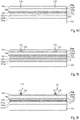
- FIGS. 1A to 1K are cross-sectional views illustrating successive steps of a non-limiting example of implementation of such a method. Various variants are within the reach of those skilled in the art based on the indications of the present description.
- the Figure 1A schematically illustrates, in the upper part, the structure obtained at the end of steps of forming an active stack of photosensitive diode 103 on the upper face of a substrate 101.
- Stack 103 is preferably a stack of inorganic semiconductor layers.
- the stack 103 for example comprises one or more layers made of a III-V type semiconductor material.
- the stack 103 is for example an active photodiode stack sensitive in the infrared or the near infrared. As a variant, the stack 103 is an active photodiode stack sensitive in the visible.
- the stack 103 comprises, in order from the upper face of the substrate 101, a layer 103a of indium phosphide (InP) not intentionally doped, an absorption layer 103b of arsenide d indium-gallium (InGaAs), for example intrinsic or lightly doped N-type (for example of the order of 10 15 atoms/cm 3 ), and a layer 103c of indium phosphide (InP) doped N-type.
- the N-type doping level of layer 103c is between 10 16 and 10 18 atoms/cm 3 .
- layer 103b is in contact, via its lower face, with the upper face of layer 103a
- layer 103c is in contact, via its lower face, with the upper face of layer 103b.
- the substrate 101 is for example made of indium phosphide.
- Layers 103a, 103b and 103c can be formed successively by epitaxy on the upper face of substrate 101.
- Substrate 101 is then a growth substrate.
- a buffer layer, not shown, for example made of indium phosphide, can optionally act as an interface between the substrate 101 and the layer 103a.
- the buffer layer is for example in contact, by its lower face, with the upper face of the substrate 101, and, by its upper face, with the underside of layer 103a.
- the buffer layer can also be formed by epitaxy from the upper face of the substrate 101, before the formation of the layers 103a, 103b and 103c.
- the active stack can be formed in the reverse order on a growth substrate, not shown, then transferred and fixed on the substrate 101.
- the layers 103c, 103b and 103a are successively formed by epitaxy on one face of the growth substrate.
- a buffer layer for example made of indium phosphide, can optionally act as an interface between the growth substrate and the layer 103c.
- the stack 103 is then fixed on the upper face of the substrate 101, for example by direct bonding or molecular bonding of the lower face of the layer 103a on the upper face of the substrate 101.
- the substrate 101 is a support substrate, for example made of silicon, or of any other material suitable for serving as a support for receiving the active stack 103.
- the Figure 1A further illustrates schematically, in the lower part, the structure obtained at the end of steps for forming an active stack of LEDs 113 on the upper face of a substrate 111.
- Stack 113 is preferably a stack of inorganic semiconductor layers.
- Stack 113 for example comprises one or more layers made of a III-V type semiconductor material.
- the stack 113 is for example an active stack of LEDs adapted to emit light visible, for example predominantly blue light.
- stack 113 is an active stack of gallium nitride (GaN) LEDs.
- the stack 113 comprises, in order from the upper face of the substrate 111, an N-type doped semiconductor layer 113a, forming a cathode layer of the stack of LEDs, an active layer 113b, and a p-type doped semiconductor layer 113c, forming an anode layer of the LED stack.
- Layer 113a is for example made of gallium nitride.
- the active layer 113b is for example a multiple quantum well stack (not detailed in the figure), consisting of alternating semiconductor layers of a first material, for example a type III-V material, and semiconductor layers of a second material, for example a type III-V material, each layer of the first material being sandwiched between two layers of the second material and defining a quantum well.
- Layer 113c is for example made of gallium nitride.
- the active layer 113b is for example in contact, by its lower face, with the upper face of the layer 113a.
- the layer 113c is for example in contact, by its lower face, with the upper face of the active layer 113b.
- the substrate 111 is for example made of silicon, sapphire, or gallium nitride.
- the layers 113a, 113b and 113c are successively formed by epitaxy on the upper face of the substrate 111.
- a buffer layer not shown, can possibly interface between the upper face of the substrate 111 and the lower face of the layer 113a.
- each of the layers of the active photosensitive diode stack 103 extends for example continuously and with a substantially uniform thickness over the entire upper surface of the substrate 101.
- each of the layers of the active stack of LEDs 113 extends for example continuously and with a substantially uniform thickness over the entire upper surface of the substrate 111.
- the substrates 101 and 111 for example have substantially the same lateral dimensions.
- the Figure 1A further illustrates a step of depositing a conductive layer 115 on and in contact with the upper face of the semiconductor layer 113c.
- Layer 115 forms an ohmic contact with the semiconductor material of layer 113c.
- Layer 115 is for example aluminum, nickel, or even a transparent conductive oxide, for example indium-tin oxide (ITO).
- ITO indium-tin oxide
- the metal layer 115 extends continuously and with a substantially uniform thickness over the entire upper surface of the layer 113c.
- Layer 115 can also have an optical reflector function.
- layer 115 may comprise two superposed layers respectively ensuring the function of ohmic contact with the semiconductor material of layer 113c and the function of optical reflector.
- the Figure 1A further illustrates a step of depositing a dielectric layer 117, for example of silicon oxide or silicon nitride, on and in contact with the upper face of the metallic layer 115.
- a dielectric layer 117 for example of silicon oxide or silicon nitride
- the dielectric layer 117 is extends continuously and with a substantially uniform thickness over the entire upper surface of the layer 115.
- the Figure 1A further illustrates a step of depositing a dielectric layer 105, for example of silicon oxide or silicon nitride, for example of the same material as layer 117, on and in contact with the upper face of upper layer 103c of the active photosensitive diode stack 103.
- the dielectric layer 105 extends continuously and with a thickness substantially uniform over the entire upper surface of the layer 103c.
- the figure 1B illustrates the structure obtained after a step of attaching and fixing the active stack of photosensitive diode 103 to the active stack of LEDs 113, then removing the substrate 101. During this step, the stack The photosensitive diode active 103 is carried over the active LED stack 113, using the substrate 101 as a support handle. On the figure 1B , the structure comprising the substrate 101 and the stack 103 is turned over with respect to the orientation of the Figure 1A . The stack 103 is then fixed on the stack 113.
- the stack 103 is fixed by direct bonding or molecular bonding of the lower face (in the orientation of the figure 1B , corresponding to the upper face in the orientation of the Figure 1A ) of the layer 105, on the upper face (in the orientation of the figure 1B , corresponding to the upper face in the orientation of the Figure 1A ) of layer 117.
- Substrate 101 is then removed, for example by grinding and/or chemical etching, so as to free up access to the upper face of layer 103a.
- each of the layers of the active stack of photosensitive diodes 103 extends for example continuously and with a substantially uniform thickness, over the entire surface of the active stack of LEDs 113. It will be noted that in this example , the active stacks 113 and 103 are unstructured and have not undergone any localized processing step before the transfer step. Thus, the transfer step does not require precise alignment.
- the figure 1C illustrates a step of depositing a dielectric layer 121, for example of silicon nitride or silicon oxide, on the upper face of the layer 103a, for example in contact with the upper face of the layer 103a.
- Layer 121 is for example deposited by a plasma-enhanced chemical vapor deposition (PECVD) process.
- PECVD plasma-enhanced chemical vapor deposition
- the figure 1D illustrates a step of forming localized through openings 123 in the dielectric layer 121.
- the openings 123 are for example formed by photolithography and etching.
- the openings are arranged opposite future P-type contact recovery zones corresponding to anode regions of the photosensitive diodes of the device.
- the Figure 1E illustrates a P-type doping step of localized regions 125 of layer 103a, located opposite the openings 123.
- the doping of regions 125 can be carried out by diffusion or implantation of P-type doping elements, for example zinc (Zn) or beryllium (Be), opposite the openings 123.
- An activation annealing of the doping elements can then be implemented.
- the activation annealing can be surface laser annealing, which makes it possible not to alter the quality of the bonding between the active stack of LEDs 113 and the active stack of photosensitive diodes 103.
- the doped regions of P type 125 form anode regions of the photosensitive diodes of the device. In this example, the regions 125 extend over the entire thickness of the layer 103a, and come into contact, by their lower face, with the upper face of the absorption layer 103b.
- the figure 1F illustrates a step of forming contact recovery metallizations 127 in the openings 123.
- Each metallization 127 comes into contact individually with the underlying region 125, through the corresponding opening 123.
- a metallic layer is first deposited continuously over the entire upper surface of the structure, that is to say on and in contact with the upper face of the dielectric layer 121 and in the openings 123, then removed by photolithography and etching so as to retain only the metallizations 127.
- each metallization 127 constitutes an anode electrode of a photosensitive diode 171 of the device.
- the figure 1G illustrates the structure obtained at the end of steps for forming laterally insulated conductive vias 129, passing through the active photosensitive diode stack 103. More particularly, in this example, the conductive vias 129 pass through the layer 121, the layers 103a, 103b and 103c of the stack 103, the insulating layers 105 and 117, and open onto and in contact with the upper face of the metallic layer 115.
- the production of the vias 129 comprises an etching step, from the upper face of the insulating layer 121, with through openings in the stack formed by the layers 117, 105, 103c, 103b, 103a and 121.
- the openings are for example formed by plasma etching, for example of the ICP type (from the English Inductively Coupled Plasma - inductively coupled plasma).
- a passivation step of the sides of the openings is then implemented.
- a layer 131 of an insulating material for example silicon oxide, is deposited on the side walls and at the bottom of the openings.
- a vertical anisotropic etching step can then be implemented to remove the insulating layer at the bottom of the openings, without removing it from the side walls.
- the openings are then filled with metal to form the conductive vias 129.
- the figure 1H illustrates the structure obtained at the end of a step of fixing the structure of the figure 1G on the upper face of a control integrated circuit 151, then removal of the substrate 111.
- the integrated circuit 151 may have been previously formed in and on a semiconductor substrate, for example by silicon. It includes circuits for controlling and reading the LEDs and photosensitive diodes of the device.
- the integrated circuit 151 comprises a set of elementary control and reading cells, making it possible to individually control and read each LED and each photosensitive diode of the device.
- the integrated circuit 151 is for example a CMOS (complementary metal oxide semiconductor) circuit.
- the circuit 151 comprises a plurality of metal connection pads 153 arranged on the side of its upper face. On the figure 1H , the structure comprising the active stacks 103 and 113 is inverted with respect to the orientation of the figure 1G .
- the lower face (in the orientation of the figure 1H , corresponding to the upper face in the orientation of the figure 1G ) of each metallization 127 is brought into contact with the upper face of one of the connection pads 153 of the integrated circuit 151.
- the lower face (in the orientation of the figure 1H , corresponding to the upper face in the orientation of the figure 1G ) of each conductive via 129 is brought into contact with the upper face of one of the connection pads 153.
- the fixing of the structure of the figure 1G on the integrated circuit 151 is for example obtained by hybrid direct bonding.
- direct bonding here is meant molecular bonding, without adding material between the surfaces brought into contact.
- Substrate 111 is then removed, for example by grinding and/or chemical etching, or by a laser lift-off process, so as to free up access to the upper face of layer 113a.
- the figure 1I illustrates the structure obtained at the end of a step of localized etching of the stack formed by the metallic layer 115 and the active stack of LEDs 113. During of this step only blocks 161 of the active stack of LEDs 113 are kept, corresponding respectively to the different LEDs of the device.
- the metallic layer portion 115 located under each LED 161 forms an anode electrode of the LED and is electrically connected to a pad 153 of the integrated circuit 151 via a via 129.
- the stack 113 and the metallic layer 115 are completely removed, so as to expose the upper face of the dielectric layer 117.
- the figure 1J illustrates the structure obtained at the end of a passivation step of the sides of the LEDs 161.
- a layer 163 of an insulating material for example silicon oxide, silicon nitride or alumina (Al 2 O 3 ) is deposited conformally on the side of the upper face of the structure, that is to say on the upper face of the insulating layer 117 and of the LEDs 161 and on the flanks of the LEDs 161.
- a vertical anisotropic etching step can then be implemented to remove the horizontal portions of the layer 163 while retaining the vertical portions of layer 163, covering the sides of LEDs 161.
- the figure 1J further illustrates a step of formation, in each photosensitive diode, of a localized opening 164 passing through the insulating layers 117 and 105 and releasing access to the upper face of the semiconductor layer 103c.
- the figure 1K illustrates the structure obtained at the end of steps of deposition and etching of a conductive layer 165, for example in a transparent conductive material, for example indium tin oxide (ITO), or in a sufficiently thin metal to be transparent, for example money, to forming cathode electrodes of LEDs 161 and cathode electrodes of photosensitive diodes 171 of the device.
- a transparent conductive material for example indium tin oxide (ITO)
- ITO indium tin oxide
- each LED 161 includes an electrode 165(a) disposed on and in contact with the upper face of the N-type semiconductor layer 113a.
- the electrode 165(a) extends over at least one side of the LED and over the upper face of the insulating layer 117, and comes into contact, by its lower face, with the upper face of a conductive via 129. Electrode 165(a) is thus electrically connected to a pad 153 of integrated circuit 151 via via 129.
- each photosensitive diode 171 comprises an electrode 165(b), preferably electrically insulated from the electrodes 165(a), arranged on the upper face of the insulating layer 117.
- each electrode 165 (b) comes into contact, by its lower face, with the upper face of a conductive via 129.
- the electrode 165(b) is thus electrically connected to a pad 153 of the integrated circuit 151 via the via 129.
- the electrode 165(b) further comes into contact with the upper face of the semiconductor layer 103c through the opening 164 ( figure 1J ).
- the contact on the upper face of the semiconductor layer 103c, via the electrode 165(b) and the opening 164, can be made only at the periphery of the device, the doped layer 103c then ensuring the equipotential on the entire surface of the device.
- the anode electrodes 127 and the cathode electrodes 165(b) of the photosensitive diodes 171, and the anode electrodes 115 and the cathode electrodes 165(a) of the LEDs 161 are all individually connected to connection pads 153 of the integrated circuit 151.
- the cathode electrodes 165(a) can be common to all the LEDs 161 of the device, and connected to the integrated circuit 151 at the periphery of the device, so as to limit the number of conductive vias 129 and of pads 153.
- the cathode electrodes 165(b) can be common to all the photosensitive diodes 171 of the device, and connected to the integrated circuit 151 at the periphery of the device, so as to limit the number of conductive vias 129 and of pads 153.
- the common cathode electrodes of the photosensitive diodes and the common cathode electrodes of the LEDs can be connected together.
- light conversion elements may optionally be arranged opposite LED 161, on the side of their upper face, to obtain, on the same device, pixels of emission adapted to emit in different wavelength ranges, for example red pixels, green pixels and blue pixels.
- filtering elements may optionally be arranged opposite photosensitive diodes 171, on the side of their upper face, to obtain, on the same device, detection pixels suitable for detecting radiation. in different wavelength ranges.
- each pixel of the device comprises a photosensitive diode 171 and an LED 161.
- the resolution of the display device and the resolution of the optical sensor can be different.
- the number of photosensitive diodes 171 of the device can be lower than the number of LEDs 161.
- the method described in relation to the figures 1A to 1K can be used to make interactive display devices of larger dimensions, for example a television screen, computer screen, smartphone screen, digital tablet, etc.
- a device can comprise a plurality of elementary electronic chips arranged, for example according to a matrix arrangement, on the same transfer substrate.
- the elementary chips are mounted integral with the transfer substrate and connected to electrical connection elements of the transfer substrate for their control.
- Each chip comprises one or more LEDs 161, one or more photosensitive diodes 171, and a circuit 151 for controlling said one or more LEDs and said one or more photosensitive diodes.
- Each chip corresponds for example to a pixel of the device.
- each chip comprises three individually controllable LEDs 161, respectively defining three sub-pixels adapted to respectively emit red light, green light and blue light, and a photosensitive diode 171 adapted to detect radiation infrared or near infrared.
- the figures 2A to 2G are sectional views illustrating successive steps of an example of a method of manufacturing such a device.
- the figure 2A very schematically illustrates a starting structure which corresponds to a structure of the type obtained by the method of figures 1A to 1K , comprising an integrated control circuit stage 151, surmounted by a photo-detection stage 201, itself surmounted by an emission stage 203.
- the photo-detection stage 201 comprises a plurality of photosensitive diodes 171 (not detailed on the figures 2A to 2G ) individually controllable by the integrated circuit 151.
- the emission stage comprises a plurality of LEDs 161 (not detailed on the figures 2A to 2G ) individually controllable by the integrated circuit 151.
- On the figure 2A only the electrical connection pads 153 of the integrated circuit 151, arranged on the side of the upper face of the integrated circuit 151, have been detailed.
- the figure 2B illustrates a step for gluing the structure of the figure 2A on a temporary support substrate 210, for example made of silicon.
- the structure of the figure 2A is fixed to the support substrate 210 by its face opposite to the integrated control circuit 151, that is to say by its lower face in the orientation of the figure 2B , corresponding to its upper face in the orientation of the figure 2A .
- the Fig. 2C illustrates an optional step of thinning the semiconductor substrate of the integrated circuit 151, by its face opposite to the stages 201 and 203.
- the integrated circuit 151 is initially formed in and on an SOI type substrate (of the English "Semiconductor On Insulator" - semiconductor on insulator).
- the SOI substrate comprises for example a silicon support, coated with an insulating layer, itself coated with a layer of monocrystalline silicon (not detailed in the figures).
- the components, in particular transistors, of the integrated circuit 151 can be formed in and on the silicon layer monocrystalline of the SOI substrate.
- the thinning stage of the Fig. 2C may consist in removing the support substrate from the SOI substrate, so as to retain only the monocrystalline silicon layer and the insulating layer of the SOI substrate.
- the integrated circuit 151 is formed in and on a solid silicon substrate, the thinning step then possibly consisting in reducing the thickness of the substrate, for example by grinding, from its upper face (in the direction of the Fig. 2C ).
- An insulating passivation layer (not detailed in the figure) can then be deposited on the upper face of the thinned substrate.
- the 2D figure illustrates a step of forming, on the side of the upper face of the integrated circuit 151, metal connection pads 221, connected to the connection pads 153 and/or to the connection terminals of electronic components, for example MOS transistors, of the circuit integrated circuit 151, via conductive vias not detailed in the figure, passing through the semiconductor substrate of integrated circuit 151.
- the figure 2E illustrates a step of formation, from the upper face of the integrated circuit 151, of trenches 230 vertically crossing the integrated circuit 151, the detection stage 201 and the emission stage 203, and opening onto the upper face of the substrate of temporary support 210.
- the trenches 230 laterally delimit a plurality of semiconductor chips 232 corresponding to the elementary pixel chips of the display device.
- the trenches 230 can be formed by plasma etching, by sawing, or by any other suitable cutting method.
- the figures 2F and 2G illustrate a step of fixing elementary chips 232 on the upper face of the same transfer substrate 250 of the display device.
- the transfer substrate 250 comprises, on the side of its upper face, a plurality of metal connection pads 252, intended to be fixed and connected electrically and mechanically to corresponding metal connection pads 221 of elementary chips 232.
- the structure of the figure 2E is returned ( figure 2F ) so as to place the metal connection pads 221 of elementary chips 232 opposite corresponding metal connection pads 252 of the transfer substrate 250.
- the pads 221 and 252 facing each other are then fixed and connected electrically, for example by direct bonding, by welding, by means of microtubes, or by any other suitable method.
- the elementary chips 232 are detached from the temporary support substrate 210, and the latter is removed ( figure 2G ).
- the detachment of the chips is carried out by mechanical separation or by separation by means of a laser beam.
- the pitch (distance center to center in front view) of the elementary chips 232 on the transfer substrate 250 is a multiple of the pitch of the elementary chips 232 on the substrate.
- only part of the elementary chips 232 are transferred simultaneously from the temporary support substrate 210 onto the transfer substrate 250.
- the other chips remain attached to the temporary support substrate 210 and can be transferred later on another part of the transfer substrate 250 or on another transfer substrate 250.
- the anode regions 125 and the anode metallizations 127 of the photosensitive diodes are produced after the transfer of the active stack of photosensitive diode 103 onto the active stack of LEDs 113.
- the anode regions 125 and the anode metallizations 127 of the photosensitive diodes can be produced before the transfer of the active stack of photosensitive diode 103 onto the active stack of LEDs 113. In this case, the order of the layers of the stack 103 is reversed compared to the example of the Figure 1A .
- An advantage is that the activation annealing of the dopants of the regions 125 can then be carried out before the transfer of the stack 103 onto the stack 113, which avoids any degradation of the bonding between the stack 103 and the stack 113 during annealing.
- the picture 3 schematically represents an example of a system comprising an optoelectronic device 300 according to one embodiment.
- the device 300 can be a device of the monolithic micro-screen type, for example produced by a method of the type described in relation to the figures 1A to 1K .
- the device 300 can be a device of larger dimensions, for example produced by a method of the type described in relation to the figures 2A to 2G .
- the device 300 combines an image display function and an optical capture function, for example to produce an interactive screen suitable for implementing functions of face or shape recognition, motion detection, identification, etc
- the system of picture 3 further comprises a light source 310.
- the source 310 is adapted to emit light radiation in the sensitivity range of the photosensitive diodes 171 (not detailed on the picture 3 ) of the device 300.
- the source 310 is an infrared source, for example a laser source.
- the source 310 illuminates a scene 320 of which it is desired to acquire an image.
- the light emitted by the source 310 is reflected by the scene 320 and returned to the device 300.
- the photosensitive diodes 171 of the device 300 then make it possible to acquire an image of the scene 320 and/or to measure depth information relating to the scene 320.
- the light source 310 is a remote source, that is to say it is distinct from the device 300.
- the control of the light source 310 and the control of the detection pixels of the device 300 are for example synchronized.
- the figure 4 is a sectional view schematically and partially illustrating another example of an optoelectronic device according to one embodiment.
- the optoelectronic device integrates a distributed light source emitting in the sensitivity range of the photodiodes 171, for example an infrared source. This makes it possible to dispense with the remote source 310 of the system of the picture 3 .
- the device of the figure 4 includes common elements with the device of the figure 1K . These elements will not be detailed again below, and only the differences with respect to the device of the figure 1K will be highlighted.
- LEDs 161(a) and 161(b) of the device have been shown, for example identical or similar.
- the LEDs 161(a) and 161(b) are adapted to emit light in the same range of wavelengths, for example predominantly blue light.
- the embodiments described are not limited to this particular example and the person skilled in the art will know how to adapt the example embodiment described in relation to the figure 4 to other LED emission colors 161.
- the LED 161(a) is coated, on the side of its upper face, with a photoluminescent conversion element 181(a) suitable for converting the light emitted by the LED into visible light at another wavelength, for example in red or green light in the case of an LED emitting blue light.
- LEDs emitting blue light it is possible to provide three types of visible light emission pixels adapted to respectively emit red light (by means of a photoluminescent conversion element converting the blue light emitted from the underlying LED into red light), green light (by means of a photoluminescent conversion element converting blue light emitted from the underlying LED into green light), and blue light (without conversion element).
- the LED 161(b) is for its part coated, on the side of its upper face, with a photoluminescent conversion element 181(b) suitable for converting the light emitted by the LED into light radiation in the wavelength range detected by the photosensitive diodes 171 of the device, for example infrared radiation.
- LED 161(b) defines a PIR emissive pixel of a device-integrated light source optoelectronics, adapted to cooperate with the photosensitive diodes 171 and replacing the source 310 of the system of the picture 3 .
- the device of the figure 4 can be a monolithic micro-screen type device, or a pixel of a device of larger dimensions.
- the number and the repetition step of the PIR pixels can be chosen according to the needs of the application.
- the device can comprise fewer PIR pixels than visible pixels (defined by the LEDs 161(a)) of the same emission color.
- the final device (monolithic micro-screen or extended device) comprises several PIR pixels distributed over the surface of the device.
- the conversion elements 181(a), 181(b) surmounting the LEDs 161(a), 161(b) are for example made based on quantum dots or based on perovskite materials, preferably inorganic perovskite materials, preferably epitaxial inorganic perovskite materials.
- the conversion elements based on perovskite materials are for example deposited by pulsed laser deposition (PLD).
- the figure 5 is a sectional view schematically and partially illustrating an alternative embodiment of the device of the figure 4 .
- the variant of the figure 5 differs from the example of the figure 4 in that it further comprises opaque walls 191, for example made of resin, laterally separating the emissive pixels from each other and laterally separating the emissive pixels from the detection pixels. This makes it possible in particular to prevent the light emitted by the PIR pixels from directly reaching the photosensitive diodes 171, without passing through the scene for which an image is to be acquired.
- opaque walls 191 for example made of resin
Landscapes
- Led Devices (AREA)
- Light Receiving Elements (AREA)
Applications Claiming Priority (2)
| Application Number | Priority Date | Filing Date | Title |
|---|---|---|---|
| FR2105156A FR3123153B1 (fr) | 2021-05-18 | 2021-05-18 | Procédé de fabrication d'un dispositif optoélectronique |
| FR2111484A FR3123146B1 (fr) | 2021-05-18 | 2021-10-28 | Procédé de fabrication d'un dispositif optoélectronique |
Publications (1)
| Publication Number | Publication Date |
|---|---|
| EP4092736A1 true EP4092736A1 (de) | 2022-11-23 |
Family
ID=81448991
Family Applications (1)
| Application Number | Title | Priority Date | Filing Date |
|---|---|---|---|
| EP22172229.1A Pending EP4092736A1 (de) | 2021-05-18 | 2022-05-09 | Verfahren zur herstellung einer optoelektronischen vorrichtung, entsprechende vorrichtung und system mit dieser vorrichtung |
Country Status (3)
| Country | Link |
|---|---|
| US (1) | US12261161B2 (de) |
| EP (1) | EP4092736A1 (de) |
| CN (1) | CN115377082A (de) |
Families Citing this family (4)
| Publication number | Priority date | Publication date | Assignee | Title |
|---|---|---|---|---|
| EP4092736A1 (de) * | 2021-05-18 | 2022-11-23 | Commissariat à l'énergie atomique et aux énergies alternatives | Verfahren zur herstellung einer optoelektronischen vorrichtung, entsprechende vorrichtung und system mit dieser vorrichtung |
| EP4138140B1 (de) * | 2021-08-19 | 2025-10-29 | Commissariat à l'Energie Atomique et aux Energies Alternatives | Verfahren zur herstellung einer optoelektronischen vorrichtung |
| CN114063229B (zh) * | 2021-09-30 | 2023-06-16 | 上海曦智科技有限公司 | 半导体装置 |
| US12543609B2 (en) * | 2023-07-31 | 2026-02-03 | Excellence Opto. Inc. | Common cathode electrode structure for vertical LED pixel package |
Citations (3)
| Publication number | Priority date | Publication date | Assignee | Title |
|---|---|---|---|---|
| US20170155020A1 (en) * | 2015-11-30 | 2017-06-01 | Lextar Electronics Corporation | Wavelength-converting material and application thereof |
| EP3667728A1 (de) * | 2018-12-13 | 2020-06-17 | Commissariat à l'énergie atomique et aux énergies alternatives | Verfahren zur herstellung einer vorrichtung mit lichtemittierenden und/oder lichtempfangenden dioden und mit einem selbst ausgestimmten kollimationsgitter |
| US20210134654A1 (en) * | 2010-10-13 | 2021-05-06 | Monolithic 3D Inc. | Multilevel semiconductor device and structure with waveguides |
Family Cites Families (18)
| Publication number | Priority date | Publication date | Assignee | Title |
|---|---|---|---|---|
| US8810018B2 (en) * | 2006-02-03 | 2014-08-19 | Stats Chippac Ltd. | Stacked integrated circuit package system with face to face stack configuration |
| US7982305B1 (en) * | 2008-10-20 | 2011-07-19 | Maxim Integrated Products, Inc. | Integrated circuit package including a three-dimensional fan-out / fan-in signal routing |
| US8354740B2 (en) * | 2008-12-01 | 2013-01-15 | Alpha & Omega Semiconductor, Inc. | Top-side cooled semiconductor package with stacked interconnection plates and method |
| US9064936B2 (en) * | 2008-12-12 | 2015-06-23 | Stats Chippac, Ltd. | Semiconductor device and method of forming a vertical interconnect structure for 3-D FO-WLCSP |
| US8236617B2 (en) * | 2010-06-04 | 2012-08-07 | Stats Chippac, Ltd. | Semiconductor device and method of forming thermally conductive layer between semiconductor die and build-up interconnect structure |
| US8951841B2 (en) * | 2012-03-20 | 2015-02-10 | Infineon Technologies Ag | Clip frame semiconductor packages and methods of formation thereof |
| DE102012112530A1 (de) * | 2012-12-18 | 2014-06-18 | Osram Opto Semiconductors Gmbh | Verfahren zum Herstellen von optoelektronischen Halbleiterchips und optoelektronischer Halbleiterchip |
| US8916474B2 (en) * | 2013-02-18 | 2014-12-23 | Infineon Technologies Ag | Semiconductor modules and methods of formation thereof |
| US9837380B2 (en) * | 2014-01-28 | 2017-12-05 | Infineon Technologies Austria Ag | Semiconductor device having multiple contact clips |
| US10153175B2 (en) * | 2015-02-13 | 2018-12-11 | Taiwan Semiconductor Manufacturing Company, Ltd. | Metal oxide layered structure and methods of forming the same |
| US10658277B2 (en) * | 2017-08-08 | 2020-05-19 | UTAC Headquarters Pte. Ltd. | Semiconductor package with a heat spreader and method of manufacturing thereof |
| US10134687B1 (en) * | 2017-12-14 | 2018-11-20 | Amkor Technology, Inc. | Semiconductor device and method of manufacturing a semiconductor device |
| US10969877B2 (en) * | 2018-05-08 | 2021-04-06 | Artilux, Inc. | Display apparatus |
| US20210050385A1 (en) * | 2019-08-13 | 2021-02-18 | Apple Inc. | Photodetectors Integrated into Thin-Film Transistor Backplanes |
| FR3099966B1 (fr) * | 2019-08-16 | 2021-09-24 | Commissariat Energie Atomique | Procédé de fabrication de dispositifs optoélectroniques |
| EP4092736A1 (de) * | 2021-05-18 | 2022-11-23 | Commissariat à l'énergie atomique et aux énergies alternatives | Verfahren zur herstellung einer optoelektronischen vorrichtung, entsprechende vorrichtung und system mit dieser vorrichtung |
| EP4092739B1 (de) * | 2021-05-18 | 2026-02-11 | Commissariat à l'Energie Atomique et aux Energies Alternatives | Verfahren zur herstellung einer optoelektronischen vorrichtung, entsprechende vorrichtung und system mit dieser vorrichtung |
| FR3123151B1 (fr) * | 2021-05-18 | 2024-05-10 | Commissariat Energie Atomique | Procédé de fabrication d'un dispositif optoélectronique |
-
2022
- 2022-05-09 EP EP22172229.1A patent/EP4092736A1/de active Pending
- 2022-05-11 US US17/741,713 patent/US12261161B2/en active Active
- 2022-05-16 CN CN202210528810.9A patent/CN115377082A/zh active Pending
Patent Citations (3)
| Publication number | Priority date | Publication date | Assignee | Title |
|---|---|---|---|---|
| US20210134654A1 (en) * | 2010-10-13 | 2021-05-06 | Monolithic 3D Inc. | Multilevel semiconductor device and structure with waveguides |
| US20170155020A1 (en) * | 2015-11-30 | 2017-06-01 | Lextar Electronics Corporation | Wavelength-converting material and application thereof |
| EP3667728A1 (de) * | 2018-12-13 | 2020-06-17 | Commissariat à l'énergie atomique et aux énergies alternatives | Verfahren zur herstellung einer vorrichtung mit lichtemittierenden und/oder lichtempfangenden dioden und mit einem selbst ausgestimmten kollimationsgitter |
Non-Patent Citations (2)
| Title |
|---|
| ERIC Z X LIU ET AL: "Recent progress of heterogeneous integration for semiconductor materials and microsystems", SOLID-STATE AND INTEGRATED CIRCUIT TECHNOLOGY, 2006. ICSICT '06. 8TH INTERNATIONAL CONFERENCE ON, IEEE, PI, 1 October 2006 (2006-10-01), pages 520 - 523, XP031045635, ISBN: 978-1-4244-0160-4 * |
| LIU XIAOYAN ET AL: "High-Bandwidth InGaN Self-Powered Detector Arrays toward MIMO Visible Light Communication Based on Micro-LED Arrays", ACS PHOTONICS, 18 December 2019 (2019-12-18), pages 3186 - 3195, XP055870321, Retrieved from the Internet <URL:https://pubs.acs.org/doi/pdf/10.1021/acsphotonics.9b00799> [retrieved on 20211207], DOI: 10.1021/acsphotonics.9b00799 * |
Also Published As
| Publication number | Publication date |
|---|---|
| US20220375913A1 (en) | 2022-11-24 |
| US12261161B2 (en) | 2025-03-25 |
| CN115377082A (zh) | 2022-11-22 |
Similar Documents
| Publication | Publication Date | Title |
|---|---|---|
| EP4092739B1 (de) | Verfahren zur herstellung einer optoelektronischen vorrichtung, entsprechende vorrichtung und system mit dieser vorrichtung | |
| EP4092736A1 (de) | Verfahren zur herstellung einer optoelektronischen vorrichtung, entsprechende vorrichtung und system mit dieser vorrichtung | |
| EP3455882B1 (de) | Verfahren zur herstellung einer optoelektronischen vorrichtung mit mehreren galliumnitriddioden | |
| EP3893281B1 (de) | Lichtemittierende und/oder lichtempfangende diodenarray-vorrichtung | |
| EP4092746A1 (de) | Verfahren zur herstellung einer optoelektronischen vorrichtung | |
| EP3900039A1 (de) | Optoelektronische vorrichtung zur aufnahme von bildern mit mehreren blickpunkten und/oder zur anzeige von bildern mit mehreren blickpunkten | |
| EP4138140B1 (de) | Verfahren zur herstellung einer optoelektronischen vorrichtung | |
| EP4376077B1 (de) | Anzeigevorrichtung | |
| EP4145507B1 (de) | Verfahren zur herstellung einer optoelektronischen vorrichtung und optoelektronische vorrichtung | |
| EP4138128B1 (de) | Bilderfassungsvorrichtung | |
| EP4620034A1 (de) | Monolithischer emissiver optoelektronischer chip | |
| WO2023110412A1 (fr) | Capteur d'images visibles et infrarouges et procédé de fabrication d'un tel capteur | |
| EP1677364A1 (de) | Lichtdetektor auf einer integrierten Schaltung sitzend | |
| EP4362093B1 (de) | Lichtemittierende vorrichtung und lichtempfänger | |
| EP4383338B1 (de) | Verfahren zur herstellung einer optoelektronischen vorrichtung mit einer led und einer photodiode | |
| FR3087939A1 (fr) | Capteur de lumiere | |
| EP4621847A1 (de) | Optoelektronische vorrichtung mit einer lichtemittierenden diode, die mit einem photodetektor überlagert ist | |
| EP4565039A1 (de) | Optoelektronische vorrichtung mit drei-elektroden-dioden und verfahren zu deren herstellung | |
| EP4167282A1 (de) | Verfahren zur herstellung einer optoelektronischen vorrichtung | |
| EP4191676A1 (de) | Röntgenbildgebungsvorrichtung | |
| WO2025125062A1 (fr) | Dispositif electronique de capture de rayonnements infrarouge et d'affichage d'images | |
| FR3142856A1 (fr) | Dispositif d’acquisition d’une image 2D et d’une image de profondeur d’une scène | |
| FR3142833A1 (fr) | Capteur d’images visibles et infrarouges | |
| FR3156991A1 (fr) | Dispositif électronique de capture et d’affichage d’images |
Legal Events
| Date | Code | Title | Description |
|---|---|---|---|
| PUAI | Public reference made under article 153(3) epc to a published international application that has entered the european phase |
Free format text: ORIGINAL CODE: 0009012 |
|
| STAA | Information on the status of an ep patent application or granted ep patent |
Free format text: STATUS: REQUEST FOR EXAMINATION WAS MADE |
|
| 17P | Request for examination filed |
Effective date: 20220509 |
|
| AK | Designated contracting states |
Kind code of ref document: A1 Designated state(s): AL AT BE BG CH CY CZ DE DK EE ES FI FR GB GR HR HU IE IS IT LI LT LU LV MC MK MT NL NO PL PT RO RS SE SI SK SM TR |
|
| RAP3 | Party data changed (applicant data changed or rights of an application transferred) |
Owner name: COMMISSARIAT A L'ENERGIE ATOMIQUE ET AUX ENERGIESALTERNATIVES |