EP4131361A1 - Carte de circuit imprimé céramique, élément de dissipation de chaleur et complexe aluminium-diamant - Google Patents
Carte de circuit imprimé céramique, élément de dissipation de chaleur et complexe aluminium-diamant Download PDFInfo
- Publication number
- EP4131361A1 EP4131361A1 EP21776350.7A EP21776350A EP4131361A1 EP 4131361 A1 EP4131361 A1 EP 4131361A1 EP 21776350 A EP21776350 A EP 21776350A EP 4131361 A1 EP4131361 A1 EP 4131361A1
- Authority
- EP
- European Patent Office
- Prior art keywords
- heat
- marker portion
- aluminum
- dissipating member
- circuit board
- Prior art date
- Legal status (The legal status is an assumption and is not a legal conclusion. Google has not performed a legal analysis and makes no representation as to the accuracy of the status listed.)
- Ceased
Links
Images


Classifications
-
- G—PHYSICS
- G06—COMPUTING OR CALCULATING; COUNTING
- G06K—GRAPHICAL DATA READING; PRESENTATION OF DATA; RECORD CARRIERS; HANDLING RECORD CARRIERS
- G06K19/00—Record carriers for use with machines and with at least a part designed to carry digital markings
- G06K19/02—Record carriers for use with machines and with at least a part designed to carry digital markings characterised by the selection of materials, e.g. to avoid wear during transport through the machine
-
- B—PERFORMING OPERATIONS; TRANSPORTING
- B32—LAYERED PRODUCTS
- B32B—LAYERED PRODUCTS, i.e. PRODUCTS BUILT-UP OF STRATA OF FLAT OR NON-FLAT, e.g. CELLULAR OR HONEYCOMB, FORM
- B32B15/00—Layered products comprising a layer of metal
- B32B15/01—Layered products comprising a layer of metal all layers being exclusively metallic
- B32B15/016—Layered products comprising a layer of metal all layers being exclusively metallic all layers being formed of aluminium or aluminium alloys
-
- B—PERFORMING OPERATIONS; TRANSPORTING
- B32—LAYERED PRODUCTS
- B32B—LAYERED PRODUCTS, i.e. PRODUCTS BUILT-UP OF STRATA OF FLAT OR NON-FLAT, e.g. CELLULAR OR HONEYCOMB, FORM
- B32B15/00—Layered products comprising a layer of metal
- B32B15/04—Layered products comprising a layer of metal comprising metal as the main or only constituent of a layer, which is next to another layer of the same or of a different material
- B32B15/043—Layered products comprising a layer of metal comprising metal as the main or only constituent of a layer, which is next to another layer of the same or of a different material of metal
-
- B—PERFORMING OPERATIONS; TRANSPORTING
- B32—LAYERED PRODUCTS
- B32B—LAYERED PRODUCTS, i.e. PRODUCTS BUILT-UP OF STRATA OF FLAT OR NON-FLAT, e.g. CELLULAR OR HONEYCOMB, FORM
- B32B3/00—Layered products comprising a layer with external or internal discontinuities or unevennesses, or a layer of non-planar shape; Layered products comprising a layer having particular features of form
- B32B3/26—Layered products comprising a layer with external or internal discontinuities or unevennesses, or a layer of non-planar shape; Layered products comprising a layer having particular features of form characterised by a particular shape of the outline of the cross-section of a continuous layer; characterised by a layer with cavities or internal voids ; characterised by an apertured layer
- B32B3/30—Layered products comprising a layer with external or internal discontinuities or unevennesses, or a layer of non-planar shape; Layered products comprising a layer having particular features of form characterised by a particular shape of the outline of the cross-section of a continuous layer; characterised by a layer with cavities or internal voids ; characterised by an apertured layer characterised by a layer formed with recesses or projections, e.g. hollows, grooves, protuberances, ribs
-
- G—PHYSICS
- G06—COMPUTING OR CALCULATING; COUNTING
- G06K—GRAPHICAL DATA READING; PRESENTATION OF DATA; RECORD CARRIERS; HANDLING RECORD CARRIERS
- G06K19/00—Record carriers for use with machines and with at least a part designed to carry digital markings
- G06K19/06—Record carriers for use with machines and with at least a part designed to carry digital markings characterised by the kind of the digital marking, e.g. shape, nature, code
- G06K19/06009—Record carriers for use with machines and with at least a part designed to carry digital markings characterised by the kind of the digital marking, e.g. shape, nature, code with optically detectable marking
- G06K19/06037—Record carriers for use with machines and with at least a part designed to carry digital markings characterised by the kind of the digital marking, e.g. shape, nature, code with optically detectable marking multi-dimensional coding
-
- H—ELECTRICITY
- H05—ELECTRIC TECHNIQUES NOT OTHERWISE PROVIDED FOR
- H05K—PRINTED CIRCUITS; CASINGS OR CONSTRUCTIONAL DETAILS OF ELECTRIC APPARATUS; MANUFACTURE OF ASSEMBLAGES OF ELECTRICAL COMPONENTS
- H05K1/00—Printed circuits
- H05K1/02—Details
- H05K1/0266—Marks, test patterns or identification means
- H05K1/0269—Marks, test patterns or identification means for visual or optical inspection
-
- H—ELECTRICITY
- H05—ELECTRIC TECHNIQUES NOT OTHERWISE PROVIDED FOR
- H05K—PRINTED CIRCUITS; CASINGS OR CONSTRUCTIONAL DETAILS OF ELECTRIC APPARATUS; MANUFACTURE OF ASSEMBLAGES OF ELECTRICAL COMPONENTS
- H05K7/00—Constructional details common to different types of electric apparatus
- H05K7/20—Modifications to facilitate cooling, ventilating, or heating
- H05K7/2039—Modifications to facilitate cooling, ventilating, or heating characterised by the heat transfer by conduction from the heat generating element to a dissipating body
- H05K7/205—Heat-dissipating body thermally connected to heat generating element via thermal paths through printed circuit board [PCB]
-
- H—ELECTRICITY
- H10—SEMICONDUCTOR DEVICES; ELECTRIC SOLID-STATE DEVICES NOT OTHERWISE PROVIDED FOR
- H10W—GENERIC PACKAGES, INTERCONNECTIONS, CONNECTORS OR OTHER CONSTRUCTIONAL DETAILS OF DEVICES COVERED BY CLASS H10
- H10W40/00—Arrangements for thermal protection or thermal control
- H10W40/20—Arrangements for cooling
- H10W40/22—Arrangements for cooling characterised by their shape, e.g. having conical or cylindrical projections
- H10W40/226—Arrangements for cooling characterised by their shape, e.g. having conical or cylindrical projections characterised by projecting parts, e.g. fins to increase surface area
- H10W40/228—Arrangements for cooling characterised by their shape, e.g. having conical or cylindrical projections characterised by projecting parts, e.g. fins to increase surface area the projecting parts being wire-shaped or pin-shaped
-
- H—ELECTRICITY
- H10—SEMICONDUCTOR DEVICES; ELECTRIC SOLID-STATE DEVICES NOT OTHERWISE PROVIDED FOR
- H10W—GENERIC PACKAGES, INTERCONNECTIONS, CONNECTORS OR OTHER CONSTRUCTIONAL DETAILS OF DEVICES COVERED BY CLASS H10
- H10W40/00—Arrangements for thermal protection or thermal control
- H10W40/20—Arrangements for cooling
- H10W40/25—Arrangements for cooling characterised by their materials
- H10W40/254—Diamond
-
- H—ELECTRICITY
- H10—SEMICONDUCTOR DEVICES; ELECTRIC SOLID-STATE DEVICES NOT OTHERWISE PROVIDED FOR
- H10W—GENERIC PACKAGES, INTERCONNECTIONS, CONNECTORS OR OTHER CONSTRUCTIONAL DETAILS OF DEVICES COVERED BY CLASS H10
- H10W40/00—Arrangements for thermal protection or thermal control
- H10W40/20—Arrangements for cooling
- H10W40/25—Arrangements for cooling characterised by their materials
- H10W40/255—Arrangements for cooling characterised by their materials having a laminate or multilayered structure, e.g. direct bond copper [DBC] ceramic substrates
-
- H—ELECTRICITY
- H10—SEMICONDUCTOR DEVICES; ELECTRIC SOLID-STATE DEVICES NOT OTHERWISE PROVIDED FOR
- H10W—GENERIC PACKAGES, INTERCONNECTIONS, CONNECTORS OR OTHER CONSTRUCTIONAL DETAILS OF DEVICES COVERED BY CLASS H10
- H10W40/00—Arrangements for thermal protection or thermal control
- H10W40/20—Arrangements for cooling
- H10W40/25—Arrangements for cooling characterised by their materials
- H10W40/258—Metallic materials
-
- H—ELECTRICITY
- H10—SEMICONDUCTOR DEVICES; ELECTRIC SOLID-STATE DEVICES NOT OTHERWISE PROVIDED FOR
- H10W—GENERIC PACKAGES, INTERCONNECTIONS, CONNECTORS OR OTHER CONSTRUCTIONAL DETAILS OF DEVICES COVERED BY CLASS H10
- H10W46/00—Marks applied to devices, e.g. for alignment or identification
-
- H—ELECTRICITY
- H10—SEMICONDUCTOR DEVICES; ELECTRIC SOLID-STATE DEVICES NOT OTHERWISE PROVIDED FOR
- H10W—GENERIC PACKAGES, INTERCONNECTIONS, CONNECTORS OR OTHER CONSTRUCTIONAL DETAILS OF DEVICES COVERED BY CLASS H10
- H10W70/00—Package substrates; Interposers; Redistribution layers [RDL]
- H10W70/60—Insulating or insulated package substrates; Interposers; Redistribution layers
- H10W70/62—Insulating or insulated package substrates; Interposers; Redistribution layers characterised by their interconnections
- H10W70/66—Conductive materials thereof
- H10W70/664—Carbon-based materials, e.g. fullerenes
-
- B—PERFORMING OPERATIONS; TRANSPORTING
- B32—LAYERED PRODUCTS
- B32B—LAYERED PRODUCTS, i.e. PRODUCTS BUILT-UP OF STRATA OF FLAT OR NON-FLAT, e.g. CELLULAR OR HONEYCOMB, FORM
- B32B18/00—Layered products essentially comprising ceramics, e.g. refractory products
-
- B—PERFORMING OPERATIONS; TRANSPORTING
- B32—LAYERED PRODUCTS
- B32B—LAYERED PRODUCTS, i.e. PRODUCTS BUILT-UP OF STRATA OF FLAT OR NON-FLAT, e.g. CELLULAR OR HONEYCOMB, FORM
- B32B2255/00—Coating on the layer surface
- B32B2255/06—Coating on the layer surface on metal layer
-
- B—PERFORMING OPERATIONS; TRANSPORTING
- B32—LAYERED PRODUCTS
- B32B—LAYERED PRODUCTS, i.e. PRODUCTS BUILT-UP OF STRATA OF FLAT OR NON-FLAT, e.g. CELLULAR OR HONEYCOMB, FORM
- B32B2255/00—Coating on the layer surface
- B32B2255/20—Inorganic coating
- B32B2255/205—Metallic coating
-
- B—PERFORMING OPERATIONS; TRANSPORTING
- B32—LAYERED PRODUCTS
- B32B—LAYERED PRODUCTS, i.e. PRODUCTS BUILT-UP OF STRATA OF FLAT OR NON-FLAT, e.g. CELLULAR OR HONEYCOMB, FORM
- B32B2264/00—Composition or properties of particles which form a particulate layer or are present as additives
- B32B2264/10—Inorganic particles
- B32B2264/107—Ceramic
- B32B2264/108—Carbon, e.g. graphite particles
-
- B—PERFORMING OPERATIONS; TRANSPORTING
- B32—LAYERED PRODUCTS
- B32B—LAYERED PRODUCTS, i.e. PRODUCTS BUILT-UP OF STRATA OF FLAT OR NON-FLAT, e.g. CELLULAR OR HONEYCOMB, FORM
- B32B2307/00—Properties of the layers or laminate
- B32B2307/30—Properties of the layers or laminate having particular thermal properties
- B32B2307/302—Conductive
-
- B—PERFORMING OPERATIONS; TRANSPORTING
- B32—LAYERED PRODUCTS
- B32B—LAYERED PRODUCTS, i.e. PRODUCTS BUILT-UP OF STRATA OF FLAT OR NON-FLAT, e.g. CELLULAR OR HONEYCOMB, FORM
- B32B2307/00—Properties of the layers or laminate
- B32B2307/50—Properties of the layers or laminate having particular mechanical properties
- B32B2307/538—Roughness
-
- B—PERFORMING OPERATIONS; TRANSPORTING
- B32—LAYERED PRODUCTS
- B32B—LAYERED PRODUCTS, i.e. PRODUCTS BUILT-UP OF STRATA OF FLAT OR NON-FLAT, e.g. CELLULAR OR HONEYCOMB, FORM
- B32B2457/00—Electrical equipment
- B32B2457/08—PCBs, i.e. printed circuit boards
-
- B—PERFORMING OPERATIONS; TRANSPORTING
- B32—LAYERED PRODUCTS
- B32B—LAYERED PRODUCTS, i.e. PRODUCTS BUILT-UP OF STRATA OF FLAT OR NON-FLAT, e.g. CELLULAR OR HONEYCOMB, FORM
- B32B7/00—Layered products characterised by the relation between layers; Layered products characterised by the relative orientation of features between layers, or by the relative values of a measurable parameter between layers, i.e. products comprising layers having different physical, chemical or physicochemical properties; Layered products characterised by the interconnection of layers
- B32B7/04—Interconnection of layers
- B32B7/08—Interconnection of layers by mechanical means
-
- B—PERFORMING OPERATIONS; TRANSPORTING
- B32—LAYERED PRODUCTS
- B32B—LAYERED PRODUCTS, i.e. PRODUCTS BUILT-UP OF STRATA OF FLAT OR NON-FLAT, e.g. CELLULAR OR HONEYCOMB, FORM
- B32B7/00—Layered products characterised by the relation between layers; Layered products characterised by the relative orientation of features between layers, or by the relative values of a measurable parameter between layers, i.e. products comprising layers having different physical, chemical or physicochemical properties; Layered products characterised by the interconnection of layers
- B32B7/04—Interconnection of layers
- B32B7/12—Interconnection of layers using interposed adhesives or interposed materials with bonding properties
-
- H—ELECTRICITY
- H05—ELECTRIC TECHNIQUES NOT OTHERWISE PROVIDED FOR
- H05K—PRINTED CIRCUITS; CASINGS OR CONSTRUCTIONAL DETAILS OF ELECTRIC APPARATUS; MANUFACTURE OF ASSEMBLAGES OF ELECTRICAL COMPONENTS
- H05K1/00—Printed circuits
- H05K1/02—Details
- H05K1/0201—Thermal arrangements, e.g. for cooling, heating or preventing overheating
- H05K1/0203—Cooling of mounted components
- H05K1/0204—Cooling of mounted components using means for thermal conduction connection in the thickness direction of the substrate
-
- H—ELECTRICITY
- H05—ELECTRIC TECHNIQUES NOT OTHERWISE PROVIDED FOR
- H05K—PRINTED CIRCUITS; CASINGS OR CONSTRUCTIONAL DETAILS OF ELECTRIC APPARATUS; MANUFACTURE OF ASSEMBLAGES OF ELECTRICAL COMPONENTS
- H05K1/00—Printed circuits
- H05K1/02—Details
- H05K1/0266—Marks, test patterns or identification means
-
- H—ELECTRICITY
- H05—ELECTRIC TECHNIQUES NOT OTHERWISE PROVIDED FOR
- H05K—PRINTED CIRCUITS; CASINGS OR CONSTRUCTIONAL DETAILS OF ELECTRIC APPARATUS; MANUFACTURE OF ASSEMBLAGES OF ELECTRICAL COMPONENTS
- H05K1/00—Printed circuits
- H05K1/02—Details
- H05K1/03—Use of materials for the substrate
- H05K1/0306—Inorganic insulating substrates, e.g. ceramic, glass
-
- H—ELECTRICITY
- H05—ELECTRIC TECHNIQUES NOT OTHERWISE PROVIDED FOR
- H05K—PRINTED CIRCUITS; CASINGS OR CONSTRUCTIONAL DETAILS OF ELECTRIC APPARATUS; MANUFACTURE OF ASSEMBLAGES OF ELECTRICAL COMPONENTS
- H05K2201/00—Indexing scheme relating to printed circuits covered by H05K1/00
- H05K2201/06—Thermal details
- H05K2201/066—Heatsink mounted on the surface of the printed circuit board [PCB]
-
- H—ELECTRICITY
- H05—ELECTRIC TECHNIQUES NOT OTHERWISE PROVIDED FOR
- H05K—PRINTED CIRCUITS; CASINGS OR CONSTRUCTIONAL DETAILS OF ELECTRIC APPARATUS; MANUFACTURE OF ASSEMBLAGES OF ELECTRICAL COMPONENTS
- H05K2201/00—Indexing scheme relating to printed circuits covered by H05K1/00
- H05K2201/09—Shape and layout
- H05K2201/09818—Shape or layout details not covered by a single group of H05K2201/09009 - H05K2201/09809
- H05K2201/09927—Machine readable code, e.g. bar code
-
- H—ELECTRICITY
- H05—ELECTRIC TECHNIQUES NOT OTHERWISE PROVIDED FOR
- H05K—PRINTED CIRCUITS; CASINGS OR CONSTRUCTIONAL DETAILS OF ELECTRIC APPARATUS; MANUFACTURE OF ASSEMBLAGES OF ELECTRICAL COMPONENTS
- H05K2201/00—Indexing scheme relating to printed circuits covered by H05K1/00
- H05K2201/09—Shape and layout
- H05K2201/09818—Shape or layout details not covered by a single group of H05K2201/09009 - H05K2201/09809
- H05K2201/09936—Marks, inscriptions, etc. for information
-
- H—ELECTRICITY
- H05—ELECTRIC TECHNIQUES NOT OTHERWISE PROVIDED FOR
- H05K—PRINTED CIRCUITS; CASINGS OR CONSTRUCTIONAL DETAILS OF ELECTRIC APPARATUS; MANUFACTURE OF ASSEMBLAGES OF ELECTRICAL COMPONENTS
- H05K3/00—Apparatus or processes for manufacturing printed circuits
- H05K3/0058—Laminating printed circuit boards onto other substrates, e.g. metallic substrates
- H05K3/0061—Laminating printed circuit boards onto other substrates, e.g. metallic substrates onto a metallic substrate, e.g. a heat sink
-
- H—ELECTRICITY
- H10—SEMICONDUCTOR DEVICES; ELECTRIC SOLID-STATE DEVICES NOT OTHERWISE PROVIDED FOR
- H10W—GENERIC PACKAGES, INTERCONNECTIONS, CONNECTORS OR OTHER CONSTRUCTIONAL DETAILS OF DEVICES COVERED BY CLASS H10
- H10W46/00—Marks applied to devices, e.g. for alignment or identification
- H10W46/101—Marks applied to devices, e.g. for alignment or identification characterised by the type of information, e.g. logos or symbols
- H10W46/103—Marks applied to devices, e.g. for alignment or identification characterised by the type of information, e.g. logos or symbols alphanumeric information, e.g. words, letters or serial numbers
-
- H—ELECTRICITY
- H10—SEMICONDUCTOR DEVICES; ELECTRIC SOLID-STATE DEVICES NOT OTHERWISE PROVIDED FOR
- H10W—GENERIC PACKAGES, INTERCONNECTIONS, CONNECTORS OR OTHER CONSTRUCTIONAL DETAILS OF DEVICES COVERED BY CLASS H10
- H10W46/00—Marks applied to devices, e.g. for alignment or identification
- H10W46/101—Marks applied to devices, e.g. for alignment or identification characterised by the type of information, e.g. logos or symbols
- H10W46/106—Marks applied to devices, e.g. for alignment or identification characterised by the type of information, e.g. logos or symbols digital information, e.g. bar codes
-
- H—ELECTRICITY
- H10—SEMICONDUCTOR DEVICES; ELECTRIC SOLID-STATE DEVICES NOT OTHERWISE PROVIDED FOR
- H10W—GENERIC PACKAGES, INTERCONNECTIONS, CONNECTORS OR OTHER CONSTRUCTIONAL DETAILS OF DEVICES COVERED BY CLASS H10
- H10W46/00—Marks applied to devices, e.g. for alignment or identification
- H10W46/401—Marks applied to devices, e.g. for alignment or identification for identification or tracking
-
- H—ELECTRICITY
- H10—SEMICONDUCTOR DEVICES; ELECTRIC SOLID-STATE DEVICES NOT OTHERWISE PROVIDED FOR
- H10W—GENERIC PACKAGES, INTERCONNECTIONS, CONNECTORS OR OTHER CONSTRUCTIONAL DETAILS OF DEVICES COVERED BY CLASS H10
- H10W46/00—Marks applied to devices, e.g. for alignment or identification
- H10W46/601—Marks applied to devices, e.g. for alignment or identification for use after dicing
- H10W46/607—Located on parts of packages, e.g. on encapsulations or on package substrates
-
- H—ELECTRICITY
- H10—SEMICONDUCTOR DEVICES; ELECTRIC SOLID-STATE DEVICES NOT OTHERWISE PROVIDED FOR
- H10W—GENERIC PACKAGES, INTERCONNECTIONS, CONNECTORS OR OTHER CONSTRUCTIONAL DETAILS OF DEVICES COVERED BY CLASS H10
- H10W70/00—Package substrates; Interposers; Redistribution layers [RDL]
- H10W70/60—Insulating or insulated package substrates; Interposers; Redistribution layers
- H10W70/62—Insulating or insulated package substrates; Interposers; Redistribution layers characterised by their interconnections
- H10W70/65—Shapes or dispositions of interconnections
-
- H—ELECTRICITY
- H10—SEMICONDUCTOR DEVICES; ELECTRIC SOLID-STATE DEVICES NOT OTHERWISE PROVIDED FOR
- H10W—GENERIC PACKAGES, INTERCONNECTIONS, CONNECTORS OR OTHER CONSTRUCTIONAL DETAILS OF DEVICES COVERED BY CLASS H10
- H10W70/00—Package substrates; Interposers; Redistribution layers [RDL]
- H10W70/60—Insulating or insulated package substrates; Interposers; Redistribution layers
- H10W70/67—Insulating or insulated package substrates; Interposers; Redistribution layers characterised by their insulating layers or insulating parts
- H10W70/69—Insulating materials thereof
- H10W70/692—Ceramics or glasses
Definitions
- the present invention relates to a ceramic circuit board, a heat-dissipating member, and an aluminum-diamond composite.
- ceramic circuit boards and heat-dissipating members have been used as electronic components.
- the ceramic circuit board is mounted on a heat-dissipating member.
- Various electronic elements such as Si semiconductor elements are mounted on the ceramic circuit board.
- Patent Document 1 describes that a marker pattern is formed on a ceramic circuit board.
- the marker pattern is formed by, for example, a laser.
- the marker pattern is arranged in the form of, for example, a bar code or a matrix code.
- the marker pattern indicates, for example, the model, type characteristics, performance, or size of a ceramic circuit board.
- Patent Document 2 describes that an aluminum-diamond composite is used as a heat-dissipating member such as a heat sink.
- the aluminum-diamond composite includes diamond particles and a metal containing aluminum as a main component.
- the aluminum-diamond composite includes a composited portion and a surface layer provided on both faces of the composited portion.
- the surface layer is composed of a metal containing aluminum as a main component.
- a production process for an electronic component it may be required to acquire information concerning members used for the electronic component (for example, a ceramic circuit board, a heat-dissipating member, or an aluminum-diamond composite).
- members used for the electronic component for example, a ceramic circuit board, a heat-dissipating member, or an aluminum-diamond composite.
- An example of an object of the present invention is to acquire information concerning a member used for an electronic component by a novel method.
- Other objects of the present invention will become apparent from the description of the present specification.
- An aspect of the present invention is a ceramic circuit board including:
- thermoelectric member Another aspect of the present invention is a heat-dissipating member, the heat-dissipating member including:
- Still another aspect of the invention is an aluminum-diamond composite having a flat plate shape and including diamond particles and a metal containing aluminum as a main component,
- information concerning a member used for an electronic component can be obtained by a novel method.
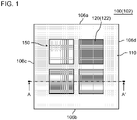
- Fig. 1 is a top view of a ceramic circuit board 100 according to Embodiment 1.
- Fig. 2 is a bottom view of the ceramic circuit board 100 shown in Fig. 1 .
- Fig. 3 is a cross-sectional view taken along the line A-A' of Fig. 1 .
- the ceramic circuit board 100 includes a marker portion 150.
- the marker portion 150 is formed on the surface of the ceramic circuit board 100. Information concerning the ceramic circuit board 100 can be acquired from the marker portion 150.
- the details of the ceramic circuit board 100 will be described by using Fig. 1 to Fig. 3 .
- the ceramic circuit board 100 includes a ceramic base material 110, a metal layer 120 (a first metal layer 122 and a second metal layer 124), and a marker portion 150.
- the ceramic circuit board 100 (ceramic base material 110) has a first surface 102, a second surface 104, and side faces (in the example shown in Fig. 1 , a first side surface 106a, a second side surface 106b, a third side surface 106c, and a fourth side surface 106d) .
- the second surface 104 is opposite to the first surface 102.
- Each side face is between the first surface 102 and the second surface 104.
- the second side surface 106b is opposite to the first side surface 106a.
- the third side surface 106c is between the first side surface 106a and the second side surface 106b.
- the fourth side surface 106d is opposite to the third side surface 106c.
- the first surface 102 and the second surface 104 of the ceramic base material 110 have a substantially rectangular shape.
- This rectangle may not be an exact rectangle, and the rectangle may have, for example, sides with sections formed therein or may have rounded corners.
- the first surface 102 and the second surface 104 of the ceramic base material 110 may have a shape other than a rectangle.
- the ceramic base material 110 is formed from, for example, AlN, Si 3 N 4 , or Al 2 O 3 .
- the thickness of the ceramic base material 110 is, for example, equal to or more than 0.2 mm and equal to or less than 1.5 mm.
- the first metal layer 122 is located on the first surface 102 of the ceramic base material 110.
- the second metal layer 124 is located on the second surface 104 of the ceramic base material 110.
- the first metal layer 122 forms a metal pattern (for example, a circuit pattern) . In the example shown in Fig. 1 , this metal pattern includes four rectangular patterns arranged adjacently. However, the metal pattern is not limited to this example.
- the second metal layer 124 extends over almost the entire second surface 104 of the ceramic base material 110. However, the area of the second metal layer 124 is slightly smaller than the area of the second surface 104.
- the area of the second metal layer 124 is, for example, equal to or more than 80% and equal to or less than 97% of the area of the second surface 104.
- the ratio of the area of the first metal layer 122 with respect to the area of the first surface 102 is smaller than the ratio of the area of the second metal layer 124 with respect to the area of the second surface 104.
- the metal layer 120 is formed from at least one selected from the group consisting of, for example, Cu, Al, Mo, an alloy including Cu and Mo, and an alloy including Cu and W.
- the thickness of the metal layer 120 is, for example, equal to or more than 0.1 mm and equal to or less than 2 mm.
- the surface of the metal layer 120 may be plated.
- the plating applied to the surface of the metal layer 120 is formed from at least one selected from the group consisting of, for example, Ni, Au, Ag, and Cu.
- the marker portion 150 is formed on the surface of the first metal layer 122. However, the marker portion 150 may be formed on the surface of the second metal layer 124 or may be formed on both the surface of the first metal layer 122 and the surface of the second metal layer 124. When the surface of the metal layer 120 (first metal layer 122 or second metal layer 124) is plated, the marker portion 150 may be formed on the surface of the plating or may be covered by the plating.
- the marker portion 150 indicates information concerning the ceramic circuit board 100.
- the information concerning the ceramic circuit board 100 is, for example, information including the production conditions for the ceramic circuit board 100.
- the information including the production conditions for the ceramic circuit board 100 includes, for example, the quality or quantity of the material used for the production of the ceramic circuit board 100, the time or temperature for heating of the ceramic circuit board 100, and the like.
- the traceability of the ceramic circuit board 100 can be enhanced by acquiring information including the production conditions for the ceramic circuit board 100 from the marker portion 150.
- the shape of the marker portion 150 is not limited to a specific shape.
- the marker portion 150 is illustratively a one-dimensional code (bar code).
- the marker portion 150 may be a two-dimensional code.
- the marker portion 150 may be both a one-dimensional code and a two-dimensional code.
- the marker portion 150 can include so much information concerning the ceramic circuit board 100.
- the marker portion 150 may include, for example, at least one selected from the group consisting of letters, numbers, and symbols.
- the marker portion 150 can include various structures formed on the surface of the ceramic base material 110.
- the marker portion 150 is a recess portion formed on the surface of a metal layer 120 (first metal layer 122) of a ceramic base material 110.
- the recess portion is formed, for example, by a laser on the surface of the metal layer 120 (first metal layer 122) of the ceramic base material 110.
- the recess portion may be formed by a method other than a laser, such as etching. By using a laser, equipment can be easily added into the line of continuous processes, and thus the marker portion 150 can be easily added without impairing productivity by adding a new process.
- the recess portion is a recess portion formed by a laser
- the marker portion (recess portion) can be formed in a region as small as equal to or more than 1 mm 2 and equal to or less than 100 mm 2
- the marker portion (recess portion) can be easily provided even in a narrow region that does not affect the performance of the product.
- Examples of the narrow region that does not affect the performance of the product may include sites that are not used for assembling, such as soldering and wire bonding.
- a code such as a two-dimensional code with a laser
- a large amount of information can be recorded even in a small marker portion.
- a laser for example, a recess portion having a width of equal to or more than 10 um and equal to or less than 200 um and a depth of equal to or more than 10 um and equal to or less than 200 um can be formed, and thus a code can be formed in a small region.
- These recess portions formed by lasers are useful also in other embodiments.
- the marker portion 150 may be formed by a coating material.
- the coating material is, for example, a solder resist and is applied by, for example, inkjetting.
- Fig. 4 is a top view of a heat-dissipating member 200 according to Embodiment 2.
- Fig. 5 is a cross-sectional view taken along the line B-B' of Fig. 4 .
- the heat-dissipating member 200 includes a first surface 202 and a second surface 204.
- the second surface 204 is opposite to the first surface 202.
- a heat-dissipating fin 210 is attached to the first surface 202 via grease 212.
- the heat-dissipating fin 210 is attached to the first surface 202 via the grease 212, after an electronic element (not shown in the drawings) such as a Si semiconductor element is mounted on the second surface 204 via a ceramic circuit board (for example, the ceramic circuit board 100 of Embodiment 1) (not shown in the drawings), to form a power module by the heat-dissipating member 200, the ceramic circuit board, and the electronic element.
- the heat-dissipating fin 210 may be screwed to the first surface 202 of the heat-dissipating member 200.
- a marker portion 250 is formed on the second surface 204. Information concerning the heat-dissipating member 200 can be acquired from the marker portion 250.
- the marker portion 250 is formed on the surface opposite to the heat-dissipating fin 210 (second surface 204), the marker portion 250 does not interfere with the heat conduction from the heat-dissipating member 200 to the heat-dissipating fin 210.
- the heat-dissipating member 200 has a first surface 202, a second surface 204, and side faces (in the example shown in Fig. 4 , a first side surface 206a, a second side surface 206b, a third side surface 206c, and a fourth side surface 206d). Each side face is between the first surface 202 and the second surface 204.
- the second side surface 206b is opposite to the first side surface 206a.
- the third side surface 206c is between the first side surface 206a and the second side surface 206b.
- the fourth side surface 206d is opposite to the third side surface 206c.
- the second surface 204 of the heat-dissipating member 200 has a substantially rectangular shape. This rectangle may not be an exact rectangle, and the rectangle may have, for example, sides with sections formed therein or may have rounded corners.
- the second surface 204 of the heat-dissipating member 200 may have a shape other than a rectangle.
- the heat-dissipating member 200 is composed of, for example, a metal base composite composed of a metal containing Al or Mg as a main component (for example, equal to or more than 85% by mass) and at least one selected from the group consisting of SiC, Si 3 N 4 , Al 2 O 3 , SiO 2 , and AlN; an alloy including Cu and Mo or an alloy including Cu and W (for example, Cu/Mo or Cu/W alloy); or a multilayer metal plate formed from Cu and Mo or Cu and W (Cu/Mo or Cu/W multilayer metal plate).
- a metal base composite composed of a metal containing Al or Mg as a main component (for example, equal to or more than 85% by mass) and at least one selected from the group consisting of SiC, Si 3 N 4 , Al 2 O 3 , SiO 2 , and AlN; an alloy including Cu and Mo or an alloy including Cu and W (for example, Cu/Mo or Cu/W alloy); or a multilayer metal plate formed from Cu
- the coefficient of linear expansion of the heat-dissipating member 200 is, for example, equal to or more than 5 ⁇ 10 -6 /K and equal to or less than 9 ⁇ 10 -6 /K.
- the thermal conductivity of the heat-dissipating member 200 is, for example, equal to or more than 150 W/mK.
- the surface of the heat-dissipating member 200 (for example, a first surface 202, a second surface 204, a first side surface 206a, a second side surface 206b, a third side surface 206c, and a fourth side surface 206d) is plated.
- the plating applied to the surface of the heat-dissipating member 200 is formed from at least one selected from the group consisting of, for example, Ni, Au, Ag, and Cu.
- the marker portion 250 may be formed on the surface of the plating or may be covered with the plating.
- the marker portion 250 indicates information concerning the heat-dissipating member 200.
- the information concerning the heat-dissipating member 200 is, for example, information including the direction of warpage of the heat-dissipating member 200.
- the marker portion 250 is located on the second surface 204 side.
- the heat-dissipating member 200 is warped convexly from the first surface 202 toward the second surface 204, and the heat-dissipating fin 210 is attached to the first surface 202, the heat-dissipating fin 210 is not in with the heat-dissipating member 200 well, and satisfactory heat dissipation by the heat-dissipating fin 210 is not realized.
- the heat-dissipating member 200 is warped convexly from the second surface 204 toward the first surface 202, and the heat-dissipating fin 210 is attached to the first surface 202, the heat-dissipating fin 210 is in contact with the heat-dissipating member 200 well, and satisfactory heat dissipation by the heat-dissipating fin 210 is realized.
- the manufacturer of the electronic component can determine that it is preferable to attach the heat-dissipating fin 210 to the surface opposite to the marker portion 250 (that is, the first surface 202).
- the information concerning the heat-dissipating member 200 is, for example, information including the production conditions for the heat-dissipating member 200.
- the information including the production conditions for the heat-dissipating member 200 includes, for example, the quality or quantity of the material used for the production of the heat-dissipating member 200, the time or temperature for heating of the heat-dissipating member 200, and the like.
- the traceability of the heat-dissipating member 200 can be enhanced by acquiring the information including the production conditions for the heat-dissipating member 200 from the marker portion 250.
- the shape of the marker portion 250 is not limited to a specific shape.
- the marker portion 250 is illustratively a one-dimensional code (bar code).
- the marker portion 250 may be a two-dimensional code.
- the marker portion 250 may be both a one-dimensional code and a two-dimensional code.
- the marker portion 250 can include so much information concerning the heat-dissipating member 200.
- the marker portion 250 may include, for example, at least one selected from the group consisting of letters, numbers, and symbols.
- the marker portion 250 can include various structures formed on the surface of the heat-dissipating member 200.
- the marker portion 250 is a recess portion formed on the surface (second surface 204) of the heat-dissipating member 200.
- the recess portion is formed by, for example, a laser on the surface (second surface 204) of the heat-dissipating member 200.
- the recess portion may be formed by a method other than a laser, such as etching.
- the marker portion 250 may be formed by a coating material.
- the coating material may be, for example, the same as the coating material used for the marker portion 150 of Embodiment 1.
- Fig. 6 is a top view of an aluminum-diamond composite 300 according to Embodiment 3.
- Fig. 7 is a cross-sectional view taken along the line C-C' of Fig. 6 .
- the aluminum-diamond composite 300 is a flat plate including diamond particles and a metal containing aluminum as a main component.
- the aluminum-diamond composite 300 is composed of a composited portion 310 and surface layers 320 (first surface layer 322 and second surface layer 324) provided on both faces of the composited portion 310.
- the surface layer 320 is composed of a material including a metal containing aluminum as a main component.
- the aluminum-diamond composite 300 includes a marker portion 350.
- the marker portion 350 is formed on the surface of the surface layer 320. Information concerning the aluminum-diamond composite 300 can be acquired from the marker portion 350.
- the aluminum-diamond composite 300 has a first surface 302, a second surface 304, and side faces (in the example shown in Fig. 6 , a first side surface 306a, a second side surface 306b, a third side surface 306c, and a fourth side surface 306d).
- the second surface 304 is opposite to the first surface 302. Each side face is between the first surface 302 and the second surface 304.
- the second side surface 306b is opposite to the first side surface 306a.
- the third side surface 306c is between the first side surface 306a and the second side surface 306b.
- the fourth side surface 306d is opposite to the third side surface 306c.
- the first surface 302 of the aluminum-diamond composite 300 has a substantially rectangular shape. This rectangle may not be an exact rectangle, and the rectangle may have, for example, sides with sections formed therein or may have rounded corners.
- the first surface 302 of the aluminum-diamond composite 300 may have a shape other than a rectangle.
- the thickness of the aluminum-diamond composite 300 is, for example, equal to or more than 0.4 mm and equal to or less than 6 mm.
- the composited portion 310 is a composited portion of diamond particles and an aluminum alloy.
- the content of the diamond particles is, for example, equal to or more than 40% by volume and equal to or less than 75% by volume with respect to the total volume of the aluminum-diamond composite 300.
- the aluminum alloy is a metal containing aluminum as a main component.
- the aluminum alloy includes, for example, equal to or more than 75% by mass of aluminum with respect to the total mass of the aluminum alloy.
- the aluminum alloy may include equal to or more than 5% by mass and equal to or less than 25% by mass of silicon with respect to the total mass of the aluminum alloy.
- the aluminum alloy may further include magnesium.
- the surface layer 320 is composed of a material including a metal containing aluminum as a main component.
- the surface layer 320 includes, for example, equal to or more than 80% by volume of the metal with respect to the total volume of the surface layer 320.
- the surface roughness Ra of the surface layer 320 is, for example, equal to or less than 1 um.
- a Ni plating layer or two layers of Ni plating and Au plating may be formed with a thickness of, for example, equal to or more than 0.5 um and equal to or less than 10 ⁇ m.
- the marker portion 350 indicates information concerning the aluminum-diamond composite 300.
- the information concerning the aluminum-diamond composite 300 is, for example, information including the production conditions for the aluminum-diamond composite 300.
- the information including the production conditions for the aluminum-diamond composite 300 includes, for example, the quality or quantity of the material used in the production of the aluminum-diamond composite 300, the time or temperature for heating of the aluminum-diamond composite 300, and the like.
- the traceability of the aluminum-diamond composite 300 can be enhanced by acquiring the information including the production conditions for the aluminum-diamond composite 300 from the marker portion 350.
- the shape of the marker portion 350 is not limited to a specific shape.
- the marker portion 350 is illustratively a one-dimensional code (bar code).
- the marker portion 350 may be a two-dimensional code.
- the marker portion 350 may be both a one-dimensional code and a two-dimensional code.
- the marker portion 350 can include so much information concerning the aluminum-diamond composite 300.
- the marker portion 350 may include, for example, at least one selected from the group consisting of letters, numbers, and symbols.
- the marker portion 350 can include various structures formed on the surface of the aluminum-diamond composite 300.
- the marker portion 350 is a recess portion formed on the surface of the aluminum-diamond composite 300.
- the recess portion is formed on, for example, the aluminum-diamond composite 300 by a laser.
- the recess portion may be formed by a method other than a laser, such as etching.
- the marker portion 350 may be formed by a coating material.
- the coating material may be, for example, the same as the coating material used for the marker portion 150 of Embodiment 1.
Landscapes
- Engineering & Computer Science (AREA)
- Physics & Mathematics (AREA)
- Microelectronics & Electronic Packaging (AREA)
- General Physics & Mathematics (AREA)
- Theoretical Computer Science (AREA)
- Thermal Sciences (AREA)
- Structure Of Printed Boards (AREA)
- Cooling Or The Like Of Semiconductors Or Solid State Devices (AREA)
- Cooling Or The Like Of Electrical Apparatus (AREA)
- Geometry (AREA)
Applications Claiming Priority (2)
| Application Number | Priority Date | Filing Date | Title |
|---|---|---|---|
| JP2020055457 | 2020-03-26 | ||
| PCT/JP2021/012500 WO2021193810A1 (fr) | 2020-03-26 | 2021-03-25 | Carte de circuit imprimé céramique, élément de dissipation de chaleur et complexe aluminium-diamant |
Publications (2)
| Publication Number | Publication Date |
|---|---|
| EP4131361A1 true EP4131361A1 (fr) | 2023-02-08 |
| EP4131361A4 EP4131361A4 (fr) | 2024-02-14 |
Family
ID=77891886
Family Applications (1)
| Application Number | Title | Priority Date | Filing Date |
|---|---|---|---|
| EP21776350.7A Ceased EP4131361A4 (fr) | 2020-03-26 | 2021-03-25 | Carte de circuit imprimé céramique, élément de dissipation de chaleur et complexe aluminium-diamant |
Country Status (6)
| Country | Link |
|---|---|
| US (1) | US11983586B2 (fr) |
| EP (1) | EP4131361A4 (fr) |
| JP (1) | JP7587570B2 (fr) |
| KR (1) | KR20220159950A (fr) |
| CN (1) | CN115053638A (fr) |
| WO (1) | WO2021193810A1 (fr) |
Cited By (1)
| Publication number | Priority date | Publication date | Assignee | Title |
|---|---|---|---|---|
| WO2025021816A1 (fr) * | 2023-07-25 | 2025-01-30 | Rogers Germany Gmbh | Procédé de production et/ou de manipulation d'un substrat métal-céramique, substrat métal-céramique, système de production de substrats métal-céramique et base de données pour substrats métal-céramique |
Families Citing this family (1)
| Publication number | Priority date | Publication date | Assignee | Title |
|---|---|---|---|---|
| WO2022109552A1 (fr) * | 2020-11-18 | 2022-05-27 | Sharfi Benjamin K | Procédés, dispositifs et matériaux de refroidissement thermique à base de diamant |
Family Cites Families (24)
| Publication number | Priority date | Publication date | Assignee | Title |
|---|---|---|---|---|
| JPS62158034A (ja) * | 1986-01-07 | 1987-07-14 | 川崎製鉄株式会社 | 金属箔複合体 |
| JPH06333073A (ja) * | 1993-05-18 | 1994-12-02 | Nichion Irika Kikai Seisakusho:Kk | コードマーク読み取り装置 |
| JP3361504B2 (ja) | 2000-05-24 | 2003-01-07 | 株式会社イメ−ジパ−トナ− | カード支払自動決済システム |
| JP2002346633A (ja) * | 2001-05-29 | 2002-12-03 | Daido Steel Co Ltd | レーザーマーキング方法 |
| EP1487759B1 (fr) | 2002-03-13 | 2007-05-23 | Electrovac AG | Procede pour la production d'un substrat metal-ceramique, de preference d'un substrat cuivre-ceramique |
| WO2006049086A1 (fr) | 2004-11-01 | 2006-05-11 | Matsushita Electric Industrial Co., Ltd. | Module electroluminescent, dispositif d'eclairage et dispositif d'affichage |
| JP2006253183A (ja) | 2005-03-08 | 2006-09-21 | Hitachi Ltd | 半導体パワーモジュール |
| JP2009130156A (ja) * | 2007-11-26 | 2009-06-11 | Seiko Epson Corp | セラミック多層基板及びセラミック多層基板の製造方法 |
| EP2305400B1 (fr) * | 2008-07-17 | 2018-05-30 | Denka Company Limited | Procédé de production pour composite aluminium-diamant |
| WO2012176473A1 (fr) * | 2011-06-22 | 2012-12-27 | パナソニック株式会社 | Substrat semi-conducteur ayant des marquages de points, et son procédé de production |
| JP5523415B2 (ja) | 2011-09-06 | 2014-06-18 | 三菱電機株式会社 | 冷却機器及び静電霧化装置及び空気調和機 |
| JP2013247256A (ja) | 2012-05-28 | 2013-12-09 | Hitachi Ltd | 半導体装置およびその製造方法 |
| WO2016067390A1 (fr) * | 2014-10-29 | 2016-05-06 | 新電元工業株式会社 | Structure de dissipation de chaleur |
| US9799584B2 (en) | 2015-11-16 | 2017-10-24 | Intel Corporation | Heat spreaders with integrated preforms |
| EP3185655B8 (fr) * | 2015-12-22 | 2024-01-03 | Heraeus Electronics GmbH & Co. KG | Procédé de codage individuel de substrats métal-céramiques |
| WO2018123380A1 (fr) * | 2016-12-28 | 2018-07-05 | デンカ株式会社 | Composant de dissipation de chaleur pour élément semiconducteur |
| DE112017003669B4 (de) | 2017-02-13 | 2022-08-25 | Fuji Electric Co., Ltd. | Halbleitervorrichtung und Verfahren zur Herstellung einer Halbleitervorrichtung |
| EP3361504A1 (fr) | 2017-02-14 | 2018-08-15 | Infineon Technologies AG | Substrat pour electronique de puissance avec un marqueur, procede de fabrication dudit substrat et de detection dudit marqueur |
| JP6799479B2 (ja) * | 2017-03-03 | 2020-12-16 | Dowaメタルテック株式会社 | 金属−セラミックス回路基板の製造方法 |
| JP6760518B2 (ja) | 2017-11-17 | 2020-09-23 | 三菱電機株式会社 | 半導体モジュール |
| US10919326B2 (en) | 2018-07-03 | 2021-02-16 | Apple Inc. | Controlled ablation and surface modification for marking an electronic device |
| FR3084667B1 (fr) | 2018-08-01 | 2020-12-25 | Saint Gobain Ct Recherches | Procede de marquage d'une piece ceramique refractaire |
| JP7129304B2 (ja) | 2018-10-03 | 2022-09-01 | Toyo Tire株式会社 | タイヤ |
| CN110690176B (zh) | 2019-10-14 | 2022-01-11 | 长江存储科技有限责任公司 | 目标晶粒的区分方法及封装芯片的失效分析方法 |
-
2021
- 2021-03-25 JP JP2022510653A patent/JP7587570B2/ja active Active
- 2021-03-25 US US17/791,971 patent/US11983586B2/en active Active
- 2021-03-25 EP EP21776350.7A patent/EP4131361A4/fr not_active Ceased
- 2021-03-25 CN CN202180010953.4A patent/CN115053638A/zh active Pending
- 2021-03-25 WO PCT/JP2021/012500 patent/WO2021193810A1/fr not_active Ceased
- 2021-03-25 KR KR1020227023670A patent/KR20220159950A/ko not_active Ceased
Cited By (1)
| Publication number | Priority date | Publication date | Assignee | Title |
|---|---|---|---|---|
| WO2025021816A1 (fr) * | 2023-07-25 | 2025-01-30 | Rogers Germany Gmbh | Procédé de production et/ou de manipulation d'un substrat métal-céramique, substrat métal-céramique, système de production de substrats métal-céramique et base de données pour substrats métal-céramique |
Also Published As
| Publication number | Publication date |
|---|---|
| CN115053638A (zh) | 2022-09-13 |
| KR20220159950A (ko) | 2022-12-05 |
| EP4131361A4 (fr) | 2024-02-14 |
| JPWO2021193810A1 (fr) | 2021-09-30 |
| JP7587570B2 (ja) | 2024-11-20 |
| WO2021193810A1 (fr) | 2021-09-30 |
| US11983586B2 (en) | 2024-05-14 |
| US20230042932A1 (en) | 2023-02-09 |
Similar Documents
| Publication | Publication Date | Title |
|---|---|---|
| US7159310B2 (en) | Electronic part mounting substrate and method for producing same | |
| US20040232544A1 (en) | Semiconductor device and method of manufacturing the same | |
| US6154364A (en) | Circuit board assembly with IC device mounted thereto | |
| EP4131361A1 (fr) | Carte de circuit imprimé céramique, élément de dissipation de chaleur et complexe aluminium-diamant | |
| JP5619437B2 (ja) | 金属−セラミックス接合基板の製造方法 | |
| JP2008218938A (ja) | 金属−セラミックス接合基板 | |
| JP2005011922A (ja) | ヒートシンクを備えた両面銅貼り基板、およびこれを用いた半導体装置 | |
| US6998180B2 (en) | Package with a substrate of high thermal conductivity | |
| JP4806803B2 (ja) | 金属−セラミックス接合基板およびその製造方法 | |
| EP1518847B1 (fr) | Substrat composite aluminium-céramique et son procédé de fabrication | |
| JPH08250823A (ja) | セラミックス回路基板 | |
| JP6799392B2 (ja) | 金属−セラミックス接合基板およびその製造方法 | |
| JP2006269966A (ja) | 配線基板およびその製造方法 | |
| JP5631446B2 (ja) | 金属−セラミックス接合基板の製造方法 | |
| JPH10242330A (ja) | パワーモジュール用基板及びその製造法 | |
| JP2001298136A (ja) | ヒートシンク及び該ヒートシンク付き配線基板 | |
| KR102257877B1 (ko) | 방열판재 | |
| JP2002033555A (ja) | 多数個取りセラミック基板 | |
| KR102678847B1 (ko) | 방열 및 휨 방지를 위한 코팅층을 가진 반도체 패키지 | |
| KR102908771B1 (ko) | 세라믹 기판 유닛 및 그 제조방법 | |
| JP7796512B2 (ja) | 金属-セラミックス接合基板およびその製造方法 | |
| JP2022171255A (ja) | 金属-セラミックス接合基板およびその製造方法 | |
| JPH04225296A (ja) | 銅回路付きセラミックス基板 | |
| JP2022157227A (ja) | 金属-セラミックス接合基板およびその製造方法 | |
| JP3408606B2 (ja) | 金属ベース多層回路基板の製造方法 |
Legal Events
| Date | Code | Title | Description |
|---|---|---|---|
| STAA | Information on the status of an ep patent application or granted ep patent |
Free format text: STATUS: THE INTERNATIONAL PUBLICATION HAS BEEN MADE |
|
| PUAI | Public reference made under article 153(3) epc to a published international application that has entered the european phase |
Free format text: ORIGINAL CODE: 0009012 |
|
| STAA | Information on the status of an ep patent application or granted ep patent |
Free format text: STATUS: REQUEST FOR EXAMINATION WAS MADE |
|
| 17P | Request for examination filed |
Effective date: 20221013 |
|
| AK | Designated contracting states |
Kind code of ref document: A1 Designated state(s): AL AT BE BG CH CY CZ DE DK EE ES FI FR GB GR HR HU IE IS IT LI LT LU LV MC MK MT NL NO PL PT RO RS SE SI SK SM TR |
|
| DAV | Request for validation of the european patent (deleted) | ||
| DAX | Request for extension of the european patent (deleted) | ||
| RIC1 | Information provided on ipc code assigned before grant |
Ipc: H05K 1/03 20060101ALN20230906BHEP Ipc: H01L 23/15 20060101ALN20230906BHEP Ipc: H01L 23/544 20060101ALI20230906BHEP Ipc: H01L 23/373 20060101ALI20230906BHEP Ipc: H05K 3/00 20060101ALI20230906BHEP Ipc: H05K 1/02 20060101ALI20230906BHEP Ipc: H01L 23/36 20060101ALI20230906BHEP Ipc: H01L 23/13 20060101AFI20230906BHEP |
|
| A4 | Supplementary search report drawn up and despatched |
Effective date: 20240115 |
|
| RIC1 | Information provided on ipc code assigned before grant |
Ipc: H05K 1/03 20060101ALN20240109BHEP Ipc: H01L 23/15 20060101ALN20240109BHEP Ipc: H01L 23/544 20060101ALI20240109BHEP Ipc: H01L 23/373 20060101ALI20240109BHEP Ipc: H05K 3/00 20060101ALI20240109BHEP Ipc: H05K 1/02 20060101ALI20240109BHEP Ipc: H01L 23/36 20060101ALI20240109BHEP Ipc: H01L 23/13 20060101AFI20240109BHEP |
|
| STAA | Information on the status of an ep patent application or granted ep patent |
Free format text: STATUS: EXAMINATION IS IN PROGRESS |
|
| 17Q | First examination report despatched |
Effective date: 20240806 |
|
| REG | Reference to a national code |
Ref country code: DE Ref legal event code: R003 |
|
| STAA | Information on the status of an ep patent application or granted ep patent |
Free format text: STATUS: THE APPLICATION HAS BEEN REFUSED |
|
| 18R | Application refused |
Effective date: 20250403 |