EP4205902A1 - Verfahren zur herstellung eines verarbeiteten substrats, verfahren zur herstellung eines halbleiterelements und zusammensetzung zur bildung einer temporären haftschicht - Google Patents
Verfahren zur herstellung eines verarbeiteten substrats, verfahren zur herstellung eines halbleiterelements und zusammensetzung zur bildung einer temporären haftschicht Download PDFInfo
- Publication number
- EP4205902A1 EP4205902A1 EP21861699.3A EP21861699A EP4205902A1 EP 4205902 A1 EP4205902 A1 EP 4205902A1 EP 21861699 A EP21861699 A EP 21861699A EP 4205902 A1 EP4205902 A1 EP 4205902A1
- Authority
- EP
- European Patent Office
- Prior art keywords
- adhesive layer
- temporary adhesive
- base material
- forming
- manufacturing
- Prior art date
- Legal status (The legal status is an assumption and is not a legal conclusion. Google has not performed a legal analysis and makes no representation as to the accuracy of the status listed.)
- Withdrawn
Links
Images
Classifications
-
- B—PERFORMING OPERATIONS; TRANSPORTING
- B24—GRINDING; POLISHING
- B24B—MACHINES, DEVICES, OR PROCESSES FOR GRINDING OR POLISHING; DRESSING OR CONDITIONING OF ABRADING SURFACES; FEEDING OF GRINDING, POLISHING, OR LAPPING AGENTS
- B24B7/00—Machines or devices designed for grinding plane surfaces on work, including polishing plane glass surfaces; Accessories therefor
- B24B7/04—Machines or devices designed for grinding plane surfaces on work, including polishing plane glass surfaces; Accessories therefor involving a rotary work-table
-
- H—ELECTRICITY
- H10—SEMICONDUCTOR DEVICES; ELECTRIC SOLID-STATE DEVICES NOT OTHERWISE PROVIDED FOR
- H10P—GENERIC PROCESSES OR APPARATUS FOR THE MANUFACTURE OR TREATMENT OF DEVICES COVERED BY CLASS H10
- H10P72/00—Handling or holding of wafers, substrates or devices during manufacture or treatment thereof
- H10P72/70—Handling or holding of wafers, substrates or devices during manufacture or treatment thereof for supporting or gripping
- H10P72/74—Handling or holding of wafers, substrates or devices during manufacture or treatment thereof for supporting or gripping using temporarily an auxiliary support
-
- B—PERFORMING OPERATIONS; TRANSPORTING
- B24—GRINDING; POLISHING
- B24B—MACHINES, DEVICES, OR PROCESSES FOR GRINDING OR POLISHING; DRESSING OR CONDITIONING OF ABRADING SURFACES; FEEDING OF GRINDING, POLISHING, OR LAPPING AGENTS
- B24B37/00—Lapping machines or devices; Accessories
- B24B37/04—Lapping machines or devices; Accessories designed for working plane surfaces
-
- H—ELECTRICITY
- H10—SEMICONDUCTOR DEVICES; ELECTRIC SOLID-STATE DEVICES NOT OTHERWISE PROVIDED FOR
- H10P—GENERIC PROCESSES OR APPARATUS FOR THE MANUFACTURE OR TREATMENT OF DEVICES COVERED BY CLASS H10
- H10P72/00—Handling or holding of wafers, substrates or devices during manufacture or treatment thereof
- H10P72/70—Handling or holding of wafers, substrates or devices during manufacture or treatment thereof for supporting or gripping
- H10P72/74—Handling or holding of wafers, substrates or devices during manufacture or treatment thereof for supporting or gripping using temporarily an auxiliary support
- H10P72/7416—Handling or holding of wafers, substrates or devices during manufacture or treatment thereof for supporting or gripping using temporarily an auxiliary support used during dicing or grinding
-
- H—ELECTRICITY
- H10—SEMICONDUCTOR DEVICES; ELECTRIC SOLID-STATE DEVICES NOT OTHERWISE PROVIDED FOR
- H10P—GENERIC PROCESSES OR APPARATUS FOR THE MANUFACTURE OR TREATMENT OF DEVICES COVERED BY CLASS H10
- H10P72/00—Handling or holding of wafers, substrates or devices during manufacture or treatment thereof
- H10P72/70—Handling or holding of wafers, substrates or devices during manufacture or treatment thereof for supporting or gripping
- H10P72/74—Handling or holding of wafers, substrates or devices during manufacture or treatment thereof for supporting or gripping using temporarily an auxiliary support
- H10P72/744—Details of chemical or physical process used for separating the auxiliary support from a device or a wafer
- H10P72/7442—Separation by peeling
Definitions
- the present invention relates to a manufacturing method of a processed base material, a manufacturing method of a semiconductor element, and a composition for forming a temporary adhesive layer.
- the base material is processed after manufacturing a laminate including a support, a temporary adhesive layer, and the base material in this order.
- a method of forming the temporary adhesive layer on one of the base material and the support and contacting the other of the base material and the support with the temporary adhesive layer is used.
- JP2017-103441A discloses a method for flattening a device silicon substrate with a bump, which goes through the following steps.
- JP2012-174956A discloses a manufacturing method of a semiconductor device, including (a) a step of applying a resin member onto a first main surface of a semiconductor wafer having a step structure on the first main surface, (b) a step of flattening a surface of the resin member by heating the resin member, in which the resin member is formed also on a side surface of the semiconductor wafer, (c) a step of performing a thinning process for the semiconductor wafer on a second main surface of the semiconductor wafer after the step (b), and (d) a step of removing the resin member from the semiconductor wafer after the step (c).
- the temporary adhesive layer itself may have a step.
- the temporary adhesive layer having such a step is subjected to polishing and grinding, and the surface thereof may be flattened.
- An object of the present invention is to provide a manufacturing method of a processed base material, in which workability of a base material is excellent, a manufacturing method of a semiconductor element, which includes the manufacturing method of a processed base material, and a composition for forming a temporary adhesive layer, in which workability of a base material is excellent.
- An object of the present invention is to provide a manufacturing method of a processed base material, in which workability of a base material is excellent, a manufacturing method of a semiconductor element, which includes the manufacturing method of a processed base material, and a composition for forming a temporary adhesive layer, in which workability of a base material is excellent.
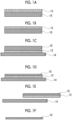
- Figs. 1A to 1F are schematic cross-sectional diagrams showing an example of a manufacturing method of a processed base material according to the embodiment of the present invention.
- a numerical range expressed using the term "to” means a range which includes the preceding and succeeding numerical values of "to” as a lower limit value and an upper limit value, respectively.
- step is meant to include not only an independent step, but also a step which cannot be clearly distinguished from other steps as long as an intended action of the step is achieved.
- the description means that the group (atomic group) includes both a group (atomic group) having no substituent and a group having a substituent.
- the description means that the alkyl group includes both an alkyl group having no substituent (unsubstituted alkyl group) and an alkyl group having a substituent (substituted alkyl group).
- exposure is meant to include not only drawing using light but also drawing using particle rays such as electron beams and ion beams.
- energy rays used for the drawing include actinic rays such as a bright line spectrum of a mercury lamp, far ultraviolet rays typified by an excimer laser, extreme ultraviolet rays (EUV light), and X-rays, and particle rays such as electron beams and ion beams.
- (meth)acrylate means both “acrylate” and “methacrylate” or either of them
- (meth)acryl means both “acryl” and “methacryl” or either of them
- (meth)acryloyl means both “acryloyl” and “methacryloyl” or either of them.
- a solid content in a composition means components other than a solvent, and a content (concentration) of the solid content in the composition is represented by the mass percentage of the components other than the solvent with respect to the total mass of the composition, unless otherwise specified.
- a temperature is 23°C and an atmospheric pressure is 101,325 Pa (1 atm), unless otherwise specified.
- a weight-average molecular weight (Mw) and a number-average molecular weight (Mn) are each expressed as a value in terms of polystyrene according to gel permeation chromatography (GPC measurement), unless otherwise specified.
- the weight-average molecular weight (Mw) and the number-average molecular weight (Mn) can be determined, for example, by using HLC-8220 (manufactured by TOSOH CORPORATION), and, as columns, GUARD COLUMN HZ-L, TSKgel Super HZM-M, TSKgel Super HZ4000, TSKgel Super HZ3000, and TSKgel Super HZ2000 (manufactured by TOSOH CORPORATION).
- the measurement is performed using tetrahydrofuran (THF) as an eluent, unless otherwise specified.
- THF tetrahydrofuran
- UV rays ultraviolet rays having a wavelength of 254 nm is used, unless otherwise specified.
- the manufacturing method of a processed base material is a manufacturing method of a processed base material, including: a step of forming a temporary adhesive layer by applying a composition for forming a temporary adhesive layer onto a surface of one member of a base material or a support; a step of flattening a surface of the temporary adhesive layer on a side opposite to a surface in contact with the base material or a surface of the temporary adhesive layer on a side opposite to a surface in contact with the support by at least one unit of polishing or grinding; a step of contacting the flattened surface of the temporary adhesive layer after the flattening with a member of the base material or the support, on which the temporary adhesive layer has not been formed; and a step of processing a surface of the base material on a side opposite to a surface in contact with the temporary adhesive layer, in which the temporary adhesive layer contains an inorganic filler.
- the manufacturing method of a processed base material is excellent in workability of the base material.
- the temporary adhesive layer has a step
- processing for example, thinning
- the base material in a laminate including the support, the temporary adhesive layer, and the base material in this order workability of the base material may be reduced, such as breakage in the base material.
- the thinning means reducing a thickness of the base material.
- a laminate may be produced by, after flattening a surface of the temporary adhesive layer formed on a surface of the base material or a surface of the support by polishing, grinding, or the like, bonding the temporary adhesive layer with the base material or the support, which is a member different from the member on which the temporary adhesive layer is formed, and then processing of the base material may be performed.
- the laminate including a temporary adhesive layer which has been used in the related art is flattened by polishing, grinding, or the like, devices, equipment, and the like used for the polishing or the grinding are clogged, and it is difficult to flatten the surface. As a result, the workability of the base material may be reduced.
- the temporary adhesive layer contains an inorganic filler, so that the flattening is performed smoothly, and force applied to the base material by the flattening method (polishing method or grinding method) is easily reduced during the flattening.
- the flattening method polishshing method or grinding method
- Figs. 1A to 1F are schematic cross-sectional diagrams showing an example of a manufacturing method of a processed base material according to the embodiment of the present invention.
- Fig. 1A shows an example of a state in which a base material 10 including a temporary adhesive layer 12 is formed by a step of forming the temporary adhesive layer 12 by applying a composition for forming a temporary adhesive layer onto a surface of the base material 10.
- Fig. 1A is a diagram in which the temporary adhesive layer is tentatively formed on the surface of the base material, but the present invention is not limited thereto.
- the temporary adhesive layer may be formed on a surface of the support.
- an unevenness is formed on a surface of the temporary adhesive layer 12 on a side opposite to the base material 10 side.
- the above-described unevenness is derived from, for example, an unevenness (omitted in the drawing) of the surface of the base material 10.
- Fig. 1B shows an example of a state in which a surface of the temporary adhesive layer 12 on a side opposite to a surface in contact with the base material is flattened by a step of flattening the above-described temporary adhesive layer 12 by at least one unit of polishing or grinding.
- the temporary adhesive layer 12 contains an inorganic filler, in the flattening by the at least one unit of polishing or grinding, it is considered that the clogging of devices, equipment, and the like used for the polishing or the grinding is suppressed. Therefore, it is presumed that the above-described flattening is smoothly performed, and the surface of the temporary adhesive layer 12, which is subjected to the at least one unit of polishing or grinding, is sufficiently flattened.
- Fig. 1C shows an example of a state in which a laminate including the base material 10, the temporary adhesive layer 12, and a support 14 is produced by a step of contacting the above-described flattened surface of the temporary adhesive layer 12 after the above-described flattening with the support 14.
- the step shown in Fig. 1C is a step of contacting the temporary adhesive layer 12 with the base material 10.
- Fig. 1D shows an example of a state in which the base material 10 is processed by a step of processing a surface of the above-described base material 10 on a side opposite to the surface in contact with the above-described temporary adhesive layer 12.
- the temporary adhesive layer 12 according to the present invention contains an inorganic filler, it is presumed that the surface of the temporary adhesive layer 12, which is subjected to the at least one unit of polishing or grinding, is sufficiently flattened, and the breakage and the like in the base material 10 during processing are suppressed.
- Fig. 1E shows an example of a state in which the base material 10 and the support 14 are peeled off.
- the base material 10 and the support 14 are peeled off at an interface between the temporary adhesive layer 12 and the support 14, but the peeled position is not limited thereto.
- the base material 10 and the support 14 may be peeled off at an interface between the temporary adhesive layer 12 and the base material 10, or the temporary adhesive layer 12 may be broken and the post-break temporary adhesive layer 12 may be present on both the base material 10 and the support 14.
- Fig. 1F shows an example of a state in which the temporary adhesive layer 12 is removed from the above-described base material 10.
- a processed base material 10 can be obtained.
- the manufacturing method of a processed base material according to the embodiment of the present invention includes a step (temporary adhesive layer forming step) of forming a temporary adhesive layer by applying a composition for forming a temporary adhesive layer onto a surface of one member of a base material or a support.
- the surface of one member of the base material or the support, to which the composition for forming a temporary adhesive layer is applied has an unevenness, it is more preferable to have an unevenness with a height difference of 0.1 ⁇ m or more, it is still more preferable to have an unevenness with a height difference of 1 ⁇ m or more, and it is particularly preferable to have an unevenness with a height difference of 2 ⁇ m or more.
- a shape of the above-described unevenness is not particularly limited, and examples thereof include a columnar shape, a semi-cylindrical shape, a prismatic shape, a spherical crown shape, a polyhedron shape, and a shape obtained by combining these shapes.
- the above-described height difference is a value measured as a height difference of the largest step on the surface of the base material, to which the composition for forming a temporary adhesive layer is applied, using a contact type step meter.
- the temporary adhesive layer forming step is preferably a step of forming the temporary adhesive layer by applying the composition for forming a temporary adhesive layer onto the surface of the base material.
- the base material is not particularly limited, and various base materials which can be used in a semiconductor process can be used depending on the intended use.
- a transparent substrate used for a liquid crystal display device or the like, or a semiconductor substrate used for a light emitting element, a solid-state imaging element, a semiconductor memory, or the like can be used.
- the base material may be a metal substrate, a resin substrate, or a prepreg (a sheet formed by impregnating a fiber member with a resin).
- the transparent substrate is, for example, a glass substrate such as quartz glass, alkali-free glass, soda glass, borosilicate glass, and aluminosilicate glass. Other structures such as a transparent conductive film, a reflective film, and a protective film may be formed in these transparent substrates.
- the semiconductor substrate is, for example, a substrate including silicon, sapphire, silicon carbide, gallium nitride, aluminum, amorphous aluminum oxide, polycrystalline aluminum oxide, silicon nitride, silicon oxynitride, GaAsP, GaP, AlGaAs, InGaN, GaN, AlGaN, ZnSe, AlGa, InP, ZnO, and the like.
- the metal substrate is, for example, an aluminum substrate, a copper substrate, a stainless steel substrate, or the like.
- the resin substrate is, for example, an epoxy substrate, a polycarbonate substrate, a flexible substrate (a polyimide substrate, a polyethylene naphthalate (PEN) substrate, and a polyethylene terephthalate (PET) substrate), or the like.
- the base material may include an undercoat layer at a surface layer portion on the side to which the temporary adhesive layer is applied, as necessary.
- the base material may include, for example, a semiconductor circuit at the surface layer portion on the side to which the temporary adhesive layer is applied.
- the base material may be a monolayer structure or a laminated structure.
- a thickness (in a case where a structure or the like is included, the maximum thickness) of the base material is not particularly limited, and is appropriately set according to the use of the laminate.
- the thickness of the base material is, for example, 0.3 to 2 mm.
- the upper limit of the numerical range is preferably 1.5 mm or less, more preferably 1 mm or less, and still more preferably 0.8 mm or less.
- the lower limit of the numerical range is preferably 0.4 mm or more, more preferably 0.5 mm or more, and still more preferably 0.6 mm or more.
- a shape of the base material is not particularly limited, and is appropriately set according to the use of the laminate.
- the shape of the base material is, for example, a disk shape (wafer type substrate) or a rectangular shape (panel type substrate).
- a diameter is, for example, 50 to 500 mm.
- the upper limit of the numerical range is preferably 400 mm or less, more preferably 300 mm or less, and still more preferably 250 mm or less.
- the lower limit of the numerical range is preferably 100 mm or more, more preferably 150 mm or more, and still more preferably 170 mm or more.
- a length of the maximum side is, for example, 200 to 1000 mm.
- the upper limit of the numerical range is preferably 900 mm or less, more preferably 800 mm or less, and still more preferably 700 mm or less.
- the lower limit of the numerical range is preferably 300 mm or more, more preferably 400 mm or more, and still more preferably 450 mm or more.
- the base material may have an orientation flat or a notch.
- the base material may be a base material in which a predetermined structure or semiconductor circuit is formed on the surface on which the temporary adhesive layer is formed, or may be a base material in which a predetermined structure or semiconductor circuit is formed on the surface opposite to the side on which the temporary adhesive layer is formed.
- the present invention it is also one preferred aspect of a base material in which a predetermined structure or semiconductor circuit is formed on the surface on which the temporary adhesive layer is formed.
- a base material in which a predetermined structure or semiconductor circuit is formed on the surface on which the temporary adhesive layer is formed.
- the unevenness can be flattened to improve the workability of the base material.
- the support is not particularly limited, and a support known in the art can be used without particular limitation, but the support is preferably in a form of a sheet or a film.
- a support for example, a support generally called a dicing tape can be used.
- the support may be a monolayer structure or a multilayer structure. That is, the support can include a monolayer or multilayer support film as a base. In addition, the support can include a pressure-sensitive adhesive layer formed on a support film or a support sheet.
- the support Since the support is expanded after processing of the base material (for example, thinning, dicing, and the like) to be peeled off and easily obtained, the support preferably has elasticity.
- the support in a case where a pressure-sensitive adhesive layer formed of an ultraviolet curable resin composition described later is used, the support preferably has light transmittance.
- a material of the support film constituting the support is not particularly limited, and may be appropriately selected from known polymer materials for a resin film.
- the polymer material constituting the support film for example, polyolefins such as polyethylene, polypropylene, a copolymer of ethylene and propylene, and polybutene; ethylene copolymers such as a copolymer of ethylene and vinyl acetate, a copolymer of ethylene and (meth)acrylate, a copolymer of ethylene and (meth)acrylic acid ester, and an ionomer including a copolymer of ethylene and (meth)acrylic acid metal salt; polyesters such as polyethylene terephthalate and polybutylene terephthalate; acryl such as poly(methyl methacrylate); polyvinyl chloride, polycarbonate, polyacetal, polyamide, polyimide, polyurethane, polystyrene, natural rubber, synthetic rubber, or the like is preferable.
- the support film may be composed of a mixed resin in which two or more kinds selected from these groups are mixed, or may have a structure in which two or more kinds of resins are multi-layered.
- a material of the support can be optionally selected in consideration of adhesiveness to the pressure-sensitive adhesive layer.
- a thickness of the support film or the support sheet is not particularly limited, and is, for example, preferably 50 to 300 ⁇ m.
- the upper limit of the numerical range is preferably 250 ⁇ m or less, more preferably 200 ⁇ m or less, and still more preferably 160 ⁇ m or less.
- the lower limit of the numerical range is preferably 60 ⁇ m or more, more preferably 70 ⁇ m or more, and still more preferably 90 ⁇ m or more.
- the pressure-sensitive adhesive layer which can constitute the support has sufficient pressure-sensitive adhesiveness to suppress scattering of the base material such as a semiconductor device during dicing.
- a material of the pressure-sensitive adhesive layer is not particularly limited, and a known pressure-sensitive adhesive material such as an acrylic resin, a urethane resin, and a silicone resin can be included.
- the pressure-sensitive adhesive layer preferably consists of a curable composition which is cured by applying heat or energy rays. Accordingly, the pressure-sensitive adhesive layer can be appropriately cured by applying heat or energy rays, and pressure-sensitive adhesive force with respect to the temporary adhesive layer can be reduced.
- the above-described curable composition is preferably a composition which is cured by irradiation with energy rays, and more preferably a composition which is cured by irradiation with ultraviolet rays.
- the curable composition contains, for example, a monomer or an oligomer having a polymerizable functional group, and a polymerization initiator.
- the pressure-sensitive adhesiveness of the pressure-sensitive adhesive layer can be appropriately controlled by controlling a crosslinking density of the pressure-sensitive adhesive material.
- the crosslinking density of the pressure-sensitive adhesive material can be controlled by an appropriate method such as a method of crosslinking through an appropriate crosslinking agent such as a polyfunctional isocyanate compound, an epoxy compound, a melamine compound, a metal salt compound, a metal chelate compound, an amino resin compound, and a peroxide, and a method of mixing a compound which has two or more carbon-carbon double bonds and crosslinking by irradiation with energy rays.
- an appropriate method such as a method of crosslinking through an appropriate crosslinking agent such as a polyfunctional isocyanate compound, an epoxy compound, a melamine compound, a metal salt compound, a metal chelate compound, an amino resin compound, and a peroxide, and a method of mixing a compound which has two or more carbon-carbon double bonds and crosslinking by irradiation with energy rays.
- the curable composition may contain one or two or more kinds of other additives such as a polymerization inhibitor, an antioxidant, a leveling agent, a viscosity improver, a viscosity reducer, a surfactant, and a filler, as necessary. Furthermore, from the viewpoint of improving applicability of the composition, the ultraviolet curable composition can contain a solvent.
- dicing tape including the pressure-sensitive adhesive layer composed of the curable composition are described in, for example, JP2010-251722A , the contents of which are incorporated in the present specification.
- a thickness of the pressure-sensitive adhesive layer is not particularly limited, and is, for example, preferably 5 to 100 ⁇ m.
- the upper limit of the numerical range is preferably 80 ⁇ m or less, more preferably 70 ⁇ m or less, and still more preferably 60 ⁇ m or less.
- the lower limit of the numerical range is more preferably 10 ⁇ m or more, and may be 15 ⁇ m or more or 20 ⁇ m or more.
- a thickness of the entire support is preferably 60 to 300 ⁇ m.
- the upper limit of the numerical range is preferably 250 ⁇ m or less, more preferably 200 ⁇ m or less, and still more preferably 160 ⁇ m or less.
- the lower limit of the numerical range is preferably 70 ⁇ m or more, more preferably 80 ⁇ m or more, and still more preferably 100 ⁇ m or more.
- a commercially available dicing tape shown below can also be used: HAE-1503, HAE-1603, UC-334EP-85, UC353EP-110A, UC3026M-110, and UC3044M-110B (all of which is manufactured by FURUKAWA ELECTRIC CO., LTD.), UHP-1005AT, UHP-1025M3, USP-1520MG, and UDT-1915MC (all of which is manufactured by Denka Company Limited.), and D-series (manufactured by LINTEC Corporation).
- composition for forming temporary adhesive layer [Composition for forming temporary adhesive layer]
- the composition for forming a temporary adhesive layer is a composition containing an inorganic filler, and is preferably a composition containing an inorganic filler and a resin.
- composition for forming a temporary adhesive layer Details of the composition for forming a temporary adhesive layer will be described later.
- Examples of a method for applying the composition for forming a temporary adhesive layer include a spin coating method, a slit coating method, a spiral coating method, a spray coating method, a screen printing method, an ink jet method, a cast coating method, a roll coating method, and a dropping method (drop cast).
- the application method is preferably a spin coating method, a slit coating method, or a spiral coating method.
- composition for forming a temporary adhesive layer may be applied by a method of attaching a film of a composition for forming a temporary adhesive layer, which has been formed in advance, to one surface of the base material or the support.
- composition for forming a temporary adhesive layer is applied, for example, to a region of the support, which is not bonded to the base material, an outer region of the base material, which is not used as a chip, or a region of the support, which corresponds to the outer region of the base material.
- one preferred aspect of the present invention also includes an aspect in which the composition for forming a temporary adhesive layer is applied to the entire surface of the base material or the support on the side in contact with the temporary adhesive layer.
- composition for forming a temporary adhesive layer is preferably dried after the application.
- a drying unit is not particularly limited, and examples thereof include a known hot plate, a heating type oven, and an infrared oven.
- Drying conditions can be appropriately adjusted, and for example, the drying can be performed by heating at 80°C to 270°C (preferably 150°C to 210°C) for 0.5 to 5 minutes (preferably 1 to 4 minutes).
- the temporary adhesive layer by drying the composition for forming a temporary adhesive layer while changing a temperature by 30°C or higher, after applying the composition for forming a temporary adhesive layer.
- the above-described step of forming the temporary adhesive layer is preferably a step of forming the temporary adhesive layer by drying the composition for forming a temporary adhesive layer while changing a temperature by 30°C or higher, after applying the composition for forming a temporary adhesive layer.
- the composition for forming a temporary adhesive layer according to the present invention contains an inorganic filler, since a volatilization path of the solvent in the composition for forming a temporary adhesive layer is reduced due to that, the generation of air bubbles may be suppressed by drying the composition for forming a temporary adhesive layer while changing a temperature by 30°C or higher.
- An example of the method of drying while changing the temperature by 30°C or higher is not particularly limited, and examples thereof include an aspect of drying at a temperature A for 1 to 10 minutes and then drying at a temperature B for 1 to 10 minutes.
- the above-described temperature A is preferably 60°C to 150°C, and more preferably 70°C to 120°C.
- the above-described temperature B is preferably 90°C to 180°C, and more preferably 100°C to 150°C.
- a difference between the temperature A and the temperature B is preferably 30°C or higher, more preferably 40°C or higher, and still more preferably 50°C or higher.
- the temporary adhesive layer contains an inorganic filler, and preferably contains an inorganic filler and a resin.
- the inorganic filler is not particularly limited as long as it is an inorganic substance and is contained in the temporary adhesive layer in a solid state, but it is preferable to include a metal or a metalloid atom.
- the inorganic filler examples include alumina, titania, zirconia, kaolin, calcined kaolin, talc, pagodite, diatomite, boron nitride, aluminum nitride, calcium carbonate, aluminum hydroxide, magnesium hydroxide, zinc oxide, lithopone, silicate mineral particles (preferably amorphous silica, colloidal silica, calcined gypsum, and silica), magnesium carbonate, titanium oxide, barium carbonate, barium sulfate, mica, and carbon black.
- silicate mineral particles preferably amorphous silica, colloidal silica, calcined gypsum, and silica
- the inorganic filler it is preferable to contain silica or alumina.
- a shape of the inorganic filler is not particularly limited, but is preferably in a form of particles.
- a shape of the particles is not particularly limited, but is preferably a substantially spherical shape.
- the particles may have a solid shape or a hollow shape.
- a particle diameter of the particles is not particularly limited, but a volume average particle size thereof is preferably 0.2 to 20 ⁇ m, more preferably 0.3 to 1.5 ⁇ m, and still more preferably 0.4 to 1.2 ⁇ m.
- the volume average particle size can be obtained, for example, by measurement using a dynamic light scattering method.
- a measuring device for example, a nanotrac particle size distribution measuring apparatus UPA-EX150 (manufactured by Nikkiso Co., Ltd.) can be used.
- a content of the inorganic filler with respect to the total volume of the temporary adhesive layer is not particularly limited, but is preferably 10% by volume or more, more preferably 20% by volume or more, and still more preferably 30% by volume or more.
- the upper limit of the above-described content is not particularly limited, but is preferably 90% by volume or less and more preferably 80% by volume or less.
- a density of the inorganic filler (density A), a density of the temporary adhesive layer scraped off from the laminate or the base material or the support on which the temporary adhesive layer is formed (density B), and a density of a resultant obtained by forming a layer same as the temporary adhesive layer, except that the inorganic filler is not contained, and scraping off the layer (density C) are measured by a hydrostatic weighing method according to JIS Z 8807 to obtain apparent densities thereof.
- a filler volume% satisfying a relational expression of (Density A) ⁇ (Filler volume%) + (Density C) ⁇ ⁇ 100% - (Filler volume%) ⁇ (Density B) is calculated.
- the apparent density means a "density in which a volume occupied by the substance itself and a volume of internal voids are used as a volume of density calculation".
- the content of the inorganic filler may be calculated from a cross-sectional observation image of the temporary adhesive layer.
- the temporary adhesive layer may contain one kind of inorganic filler, or two or more kinds of inorganic fillers may be used in combination. In a case where the temporary adhesive layer contains two or more kinds of inorganic fillers, the total amount thereof is preferably within the above-described range.
- the content of the inorganic filler with respect to the total mass of the temporary adhesive layer is preferably 30% to 95% by mass, more preferably 40% to 90% by mass, and still more preferably 50% to 85% by mass.
- the temporary adhesive layer preferably contains a resin.
- the temporary adhesive layer preferably contains a non-curable resin.
- the "non-curable” means property of not increasing hardness (Rockwell hardness) by the action of heat (for example, 150°C or higher, preferably 200°C or higher) or light (for example, light in at least any band in a wavelength range of 180 to 800 nm, preferably light having a wavelength of 200 to 400 nm). As a result, removal of the temporary adhesive layer is easier.
- the temporary adhesive layer preferably contains a thermoplastic resin (resin which is soft in a case of being heated to a glass transition point or a melting point). As a result, removal of the temporary adhesive layer is easier.
- a thermoplastic resin resin which is soft in a case of being heated to a glass transition point or a melting point.
- the temporary adhesive layer also preferably contains a water-insoluble resin.
- the "water-insoluble” means property in which saturated solubility (g) in 100 g of water at 23°C is 1 g or less.
- the saturated solubility in 100 g of water at 23°C is preferably 0.9 g or less, more preferably 0.5 g or less, and still more preferably 0.1 g or less.
- the saturated solubility in water at 23°C is practically 0.001 g or more, and may be 0.01 g or more.
- the temporary adhesive layer also preferably contains a transparent resin.
- the minimum light transmittance of a temporary adhesive layer having a thickness of 50 mm in a wavelength range of 400 to 700 nm is preferably 85% or more, more preferably 88% or more, and still more preferably 90% or more.
- the above-described minimum light transmittance of the temporary adhesive layer is preferably 99.9% or less, and may be 98% or less.
- the temporary adhesive layer preferably contains a non-curable and water-insoluble resin or a thermoplastic and water-insoluble resin, more preferably contains a non-curable, water-insoluble, and transparent resin or a thermoplastic, water-insoluble, and transparent resin, and still more preferably contains a thermoplastic, water-insoluble, and transparent resin.
- the temporary adhesive layer preferably contains at least one resin selected from the group consisting of polyvinyl acetal, polyalkyl methacrylate, and acyl cellulose, more preferably contains at least one resin selected from the group consisting of polyvinyl acetal and polyalkyl methacrylate, and still more preferably contains polyvinyl acetal.
- the polyvinyl acetal is preferably a resin obtained by reacting polyvinyl alcohol with an aldehyde to be acetalized, and more preferably a compound including each repeating unit represented by Formula (PV-1).
- R 1 represents an alkyl group
- R 2 to R 5 each independently represent a hydrogen atom or a monovalent substituent
- x, y, and z each represent a molar ratio (mol%) of each repeating unit in the resin
- x + y + z is 80 to 100 mol%.
- an asterisk "*" represents a bond or a terminal site between repeating units.
- R 1 is preferably an alkyl group having 1 to 10 carbon atoms, more preferably an alkyl group having 1 to 5 carbon atoms, and still more preferably an alkyl group having 2 or 3 carbon atoms.
- R 1 is a propyl group (-C 3 H 7 ), that is, the polyvinyl acetal is polyvinyl butyral.
- R 2 to R 5 are preferably a hydrogen atom.
- the monovalent substituent is preferably, for example, the following substituent T.
- R 2 's between different repeating units may be the same or different from each other
- R 3 's between different repeating units may be the same or different from each other
- R 4 's between different repeating units may be the same or different from each other
- R 5 's between different repeating units may be the same or different from each other.
- substituent T examples include one selected from a halogen atom, a cyano group, a nitro group, a hydrocarbon group, a heterocyclic group, -ORt 1 , -CORt 1 , -COORt 1 , -OCORt 1 , -NRt 1 Rt 2 , -NHCORt 1 , -CONRt 1 Rt 2 , -NHCONRt 1 Rt 2 , -NHCOORt 1 , -SRt 1 , -SO 2 Rt 1 , -SO 2 ORt 1 , -NHSO 2 Rt 1 , and -SO 2 NRt 1 Rt 2 .
- Rt 1 and Rt 2 each independently represent a hydrogen atom, a hydrocarbon group, or a heterocyclic group.
- Rt 1 and Rt 2 may be bonded to each other to form a ring.
- examples of the halogen atom include a fluorine atom, a chlorine atom, a bromine atom, and an iodine atom.
- examples of the hydrocarbon group include an alkyl group, an alkenyl group, an alkynyl group, and an aryl group.
- the number of carbon atoms in the alkyl group is preferably 1 to 10, more preferably 1 to 5, and still more preferably 1 or 2.
- the alkyl group may be linear, branched, or cyclic, and is preferably linear or branched.
- the number of carbon atoms in the alkenyl group is preferably 2 to 10, more preferably 2 to 5, and particularly preferably 2 or 3.
- the alkenyl group may be linear, branched, or cyclic, and is preferably linear or branched.
- the number of carbon atoms in the alkynyl group is preferably 2 to 10 and more preferably 2 to 5.
- the alkynyl group may be linear or branched.
- the number of carbon atoms in the aryl group is preferably 6 to 10, more preferably 6 to 8, and still more preferably 6 or 7.
- the heterocyclic group may be a single ring or a polycyclic ring.
- the heterocyclic group is preferably a single ring or a polycyclic ring having 2 to 4 rings.
- the number of heteroatoms constituting the ring of the heterocyclic group is preferably 1 to 3.
- the heteroatom constituting the ring of the heterocyclic group is preferably a nitrogen atom, an oxygen atom, or a sulfur atom.
- the number of carbon atoms constituting the ring of the heterocyclic group is preferably 3 to 10, more preferably 3 to 8, and still more preferably 3 to 5.
- the hydrocarbon group and the heterocyclic group as the substituent T may further have another substituent or may be unsubstituted.
- Examples of the other substituent here include the above-described substituents T.
- the above-described substituent T is a halogen atom (particularly, a fluorine atom, a chlorine atom, or a bromine atom), an alkyl group having 1 to 5 carbon atoms (particularly, a methyl group, an ethyl group, or a propyl group), an alkenyl group having 2 to 5 carbon atoms (particularly, an ethenyl group (vinyl group) or a propenyl group), an alkoxy group having 1 to 5 carbon atoms (particularly, a methoxy group, an ethoxy group, or a propoxy group), a hydroxyl group, a thiol group, a carbonyl group, a thiocarbonyl group, a carboxy group, an amino group, a nitro group, a phenyl group, or the like.
- a halogen atom particularly, a fluorine atom, a chlorine atom, or a bromine atom
- the substituent T is preferably a fluorine atom, a methyl group, an ethyl group, a methoxy group, an ethoxy group, a hydroxyl group, a carbonyl group, or a carboxy group. These substituents may further have another substituent or may be unsubstituted.
- x + y + z is preferably 85 to 100 mol%.
- the upper limit of the numerical range is generally 100 mol%, but may be approximately 98 mol%.
- the lower limit of the numerical range is more preferably 90 mol% or more and still more preferably 95 mol% or more. That is, the polyvinyl acetal may contain a repeating unit other than the above-described three repeating units, but a molar ratio of such other repeating units is preferably 0 to 20 mol%, more preferably 0 to 10 mol%, still more preferably 0 to 5 mol%, and particularly preferably 0 mol%.
- x corresponds to a degree of acetalization in the polyvinyl acetal resin, and is preferably 50 to 90 mol%.
- the upper limit of the numerical range is preferably 85 mol% or less, more preferably 80 mol% or less, and still more preferably 76 mol% or less.
- the lower limit of the numerical range is preferably 60 mol% or more, more preferably 65 mol% or more, and still more preferably 70 mol% or more.
- y corresponds to a content of hydroxyl group in the polyvinyl acetal resin, and is preferably 10 to 50 mol%.
- the upper limit of the numerical range is preferably 40 mol% or less, more preferably 35 mol% or less, and still more preferably 30 mol% or less.
- the lower limit of the numerical range is preferably 15 mol% or more, more preferably 20 mol% or more, and still more preferably 24 mol% or more.
- z corresponds to a content of acetyl group in the polyvinyl acetal resin, and is preferably 1 to 5 mol%.
- the upper limit of the numerical range is preferably 4 mol% or less, more preferably 3.5 mol% or less, and still more preferably 3 mol% or less.
- the lower limit of the numerical range is preferably 1.5 mol% or more, more preferably 1.7 mol% or more, and still more preferably 2 mol% or more.
- a weight-average molecular weight of the polyvinyl acetal is preferably 10,000 to 300,000.
- the upper limit of the numerical range is more preferably 200,000 or less, more preferably 150,000 or less, and particularly preferably 120,000 or less.
- the lower limit of the numerical range is preferably 20,000 or more, more preferably 50,000 or more, and still more preferably 80,000 or more.
- a content of the polyvinyl acetal in the temporary adhesive layer is preferably 5% to 50% by mass.
- the upper limit of the numerical range may be 45% by mass or less, 40% by mass or less, or 35% by mass or less.
- the lower limit of the numerical range is preferably 8% by mass or more, more preferably 10% by mass or more, and still more preferably 15% by mass or more.
- the polyvinyl acetal in the temporary adhesive layer may be composed of one kind alone or a mixture including two or more kinds of polyvinyl acetals. In a case where the polyvinyl acetal is a mixture, the total amount thereof is preferably within the above-described range.
- the polyalkyl methacrylate is more preferably a compound including each repeating unit represented by Formula (PM-1).
- R 7 represents an alkyl group
- R 8 represents a hydrogen atom or a methyl group
- R 9 represents a monovalent organic group
- p and q each represent a molar ratio of each repeating unit in the resin
- p is 60 to 100 mol%
- q is 0 to 40 mol%
- p + q is 80 to 100 mol%.
- an asterisk "*" represents a bond or a terminal site between repeating units.
- the repeating unit in which q is attached is a repeating unit which does not satisfy the requirement of the repeating unit in which p is attached.
- p is preferably 80 mol% or more, more preferably 90 mol% or more, and still more preferably 95 mol% or more.
- p may be 98 mol% or less.
- R 7 is preferably an alkyl group having 1 to 10 carbon atoms, more preferably an alkyl group having 1 to 5 carbon atoms, and still more preferably an alkyl group having 1 or 3 carbon atoms.
- R 7 is preferably a methyl group.
- R 7 's between different repeating units may be different from each other, but it is preferable to be the same.
- the polyalkyl methacrylate is preferably polymethyl methacrylate (PMMA) in which p is 90 mol% or more and R 7 is a methyl group.
- q is preferably 20 mol% or less, more preferably 10 mol% or less, and still more preferably 5 mol% or more. In addition, q may be 2 mol% or more.
- the repeating unit in which q is attached is preferably a repeating unit derived from (meth)acrylate which does not satisfy the requirement of the repeating unit in which p is attached.
- Examples of such a repeating unit include a case where, in the repeating unit in which q is attached, R 8 is a hydrogen atom, or a case where, in the repeating unit in which q is attached, R 8 is a methyl group and R 9 is -COOR10 (R10 is an organic group other than an alkyl group).
- repeating unit in which q is attached is also preferably a repeating unit represented by Formula (PM-2).
- R 8 has the same meaning as R 8 in Formula (PM-1), R 20 represents a monovalent substituent, and m represents an integer of 0 to 4.
- substituents include the above-described substituent T, and specific examples thereof include a fluorine atom, a methyl group, an ethyl group, a methoxy group, an ethoxy group, a hydroxyl group, a carbonyl group, and a carboxy group.
- these groups may further have a substituent.
- m may be 3 or less or 1 or more.
- a hydrogen atom in the polyalkyl methacrylate may be substituted with a substituent.
- substituents include the above-described substituent T, and specific examples thereof include a fluorine atom, a methyl group, an ethyl group, a methoxy group, an ethoxy group, a hydroxyl group, a carbonyl group, and a carboxy group.
- a weight-average molecular weight of the polyalkyl methacrylate is preferably 10,000 to 300,000.
- the upper limit of the numerical range is more preferably 200,000 or less, more preferably 150,000 or less, and particularly preferably 120,000 or less.
- the lower limit of the numerical range is preferably 20,000 or more, more preferably 50,000 or more, and still more preferably 80,000 or more.
- a content of the polyalkyl methacrylate in the temporary adhesive layer is preferably 5% to 50% by mass.
- the upper limit of the numerical range may be 45% by mass or less, 40% by mass or less, or 35% by mass or less.
- the lower limit of the numerical range is preferably 8% by mass or more, more preferably 10% by mass or more, and still more preferably 15% by mass or more.
- the polyalkyl methacrylate in the temporary adhesive layer may be composed of one kind alone or a mixture including two or more kinds of polyalkyl methacrylates. In a case where the polyalkyl methacrylate is a mixture, the total amount thereof is preferably within the above-described range.
- the acyl cellulose is a compound obtained by acyl-esterifying cellulose, and is more preferably a compound represented by Formula (AC-1).
- R 11 to R 16 each independently represent a hydrogen atom or an acyl group (-COR 17 ; R 17 is an alkyl group), at least one of R 11 to R 16 is an acyl group, and n represents a degree of polymerization.
- the alkyl group R 17 in the acyl group is preferably an alkyl group having 1 to 10 carbon atoms, more preferably an alkyl group having 1 to 5 carbon atoms, and still more preferably an alkyl group having 1 or 3 carbon atoms.
- R 17 is a methyl group, that is, the acyl group is an acetyl group and the acyl cellulose is cellulose acetate.
- the types of acyl groups are generally the same, but may be partially different from each other.
- R 11 to R 16 in the same repeating unit, it is preferable that at least two thereof are acyl groups, it is more preferable that at least four thereof are acyl groups, and all six may be acyl groups. Between different repeating units, the number of acyl groups may be the same or different from each other.
- An acylation degree proportion of carboxylic acid liberated by saponifying the acyl cellulose; in particular, in a case where the acyl cellulose is cellulose acetate, also referred to as an acetylation degree
- the upper limit of the numerical range is preferably 70% or less, more preferably 65% or less, and still more preferably 60% or less.
- the lower limit of the numerical range is preferably 40% or more, more preferably 45% or more, and still more preferably 50% or more.
- a degree of substitution which represents a degree of substitution of the acyl group, is preferably 0.1 to 3.
- the upper limit of the numerical range is preferably 2.9 or less, more preferably 2.8 or less, and still more preferably 2.7 or less.
- the lower limit of the numerical range is preferably 0.2 or more, more preferably 0.3 or more, and still more preferably 0.4 or more.
- the above-described degree of substitution means an average number of acetylated (acylated) groups out of three hydroxyl groups per glucose unit.
- the cellulose acetate may have, for example, the above-described substituent T.
- a hydrogen atom at the terminal in Formula (AC-1) may be substituted with a substituent (for example, another sugar).
- a weight-average molecular weight of the acyl cellulose is preferably 10,000 to 300,000.
- the upper limit of the numerical range is more preferably 200,000 or less, more preferably 150,000 or less, and particularly preferably 120,000 or less.
- the lower limit of the numerical range is preferably 20,000 or more, still more preferably 50,000 or more, and still more preferably 80,000 or more.
- a content of the acyl cellulose in the temporary adhesive layer is preferably 5% to 50% by mass.
- the upper limit of the numerical range may be 45% by mass or less, 40% by mass or less, or 35% by mass or less.
- the lower limit of the numerical range is preferably 8% by mass or more, more preferably 10% by mass or more, and still more preferably 15% by mass or more.
- the acyl cellulose in the temporary adhesive layer may be composed of one kind alone or a mixture including two or more kinds of acyl celluloses. In a case where the acyl cellulose is a mixture, the total amount thereof is preferably within the above-described range.
- an elastomer can also be used.
- the temporary adhesive layer contains an elastomer, it is possible to form a film which has excellent adhesiveness by following fine unevenness of the base material or the support and by an appropriate anchor effect.
- application of stress to the base material is suppressed, so that the base material can be easily can be easily peeled off from the support and the device or the like on the base material can be prevented from being damaged or falling off.
- the elastomer means a polymer compound exhibiting elastic deformation. That is, the elastomer is a polymer compound having a property of being instantly deformed according to an external force in a case where the external force is applied and of being recovered to an original shape in a short time in a case where the external force is removed.
- the elastomer can be elastically deformed to a length of 200% by applying an external force and pulling both ends in a case where a length of the original shape at room temperature (23°C) is set as 100%, and in a case where the external force is removed, the elastomer preferably has a property of returning to 130% of its length in a short period of time.
- a 5% thermal mass reduction temperature from 25°C at 20 °C/min is 375°C or higher, preferably 380°C or higher, more preferably 390°C or higher, and most preferably 400°C or higher.
- the upper limit value thereof is not particularly limited, but is preferably 1000°C or lower and more preferably 800°C or lower. According to this aspect, it is easy to form a film such as a sheet, having excellent heat resistance.
- the mass reduction temperature is a value measured by a thermogravimetric analyzer (TGA) under the above-described temperature rising condition in a nitrogen stream.
- TGA thermogravimetric analyzer
- the mass reduction temperature means a value in a mixture of the two or more kinds of elastomers.
- a glass transition temperature (hereinafter, also referred to as "Tg") of the elastomer is preferably -50°C to 300°C and more preferably 0°C to 200°C.
- Tg glass transition temperature
- the above-described value of Tg means a lower glass transition temperature.
- a weight-average molecular weight of the elastomer is preferably 2,000 to 200,000, more preferably 10,000 to 200,000, and particularly preferably 50,000 to 100,000.
- a residue is less likely to remain on the base material in a case where the temporary adhesive layer is removed.
- an elastomer including a repeating unit derived from styrene (polystyrene-based elastomer), a polyester-based elastomer, a polyolefin-based elastomer, a polyurethane-based elastomer, a polyamide-based elastomer, a polyacryl-based elastomer, a silicone-based elastomer, a polyimide-based elastomer, or the like can be used as the elastomer.
- At least one selected from a polystyrene-based elastomer, a polyester-based elastomer, a polyolefin-based elastomer, a polyurethane-based elastomer, a polyamide-based elastomer, a polyacryl-based elastomer, a silicone-based elastomer, or a polyimide-based elastomer is preferable, and from the viewpoint of solubility, heat resistance, and the like, a polystyrene-based elastomer is particularly preferable.
- the polystyrene-based elastomer is not particularly limited, and can be appropriately selected depending on the purpose. Examples thereof include a styrene-butadiene-styrene block copolymer (SBS), a styrene-isoprene-styrene block copolymer (SIS), a styrene-ethylene-styrene block copolymer (SEBS), a styrene-butadiene-butylene-styrene copolymer (SBBS), a hydrogenated product of these copolymers, a styrene-ethylene-propylene-styrene block copolymer (SEPS), and a styrene-ethylene-ethylene-propylene-styrene block copolymer.
- SBS styrene-butadiene-styrene block copolymer
- SIS styrene-iso
- a content of the repeating unit derived from styrene in the polystyrene-based elastomer is preferably 40% by mass or more, more preferably 45% by mass or more, and still more preferably 46% by mass or more.
- the upper limit thereof may be, for example, 90% by mass or less or 85% by mass or less.
- the polystyrene-based elastomer is preferably a block copolymer of styrene and another monomer, more preferably a block copolymer in which either or both terminals are styrene blocks, and particularly preferably a block copolymer in which both terminals are styrene blocks.
- both terminals of the polystyrene-based elastomer are styrene blocks (repeating units derived from styrene)
- the heat resistance is further improved. This is because the repeating unit derived from styrene having high heat resistance is present at the terminal.
- the polystyrene block is a reactive polystyrene-based hard block
- the polystyrene-based elastomer tends to be more excellent in heat resistance and chemical resistance, which is preferable.
- such an elastomer is more preferable from the viewpoint of solubility in a solvent and resistance to a resist solvent.
- polystyrene-based elastomer is a hydrogenated product
- stability with respect to heat is improved, and change in quality, such as decomposition and polymerization, is unlikely to occur.
- the "repeating unit derived from styrene” is a constitutional unit derived from styrene which is included in a polymer in a case of polymerizing styrene or a styrene derivative, and may have a substituent.
- the styrene derivative include ⁇ -methylstyrene, 3-methylstyrene, 4-propylstyrene, and 4-cyclohexylstyrene.
- substituents examples include an alkyl group having 1 to 5 carbon atoms, an alkoxy group having 1 to 5 carbon atoms, an alkoxyalkyl group having to 5 carbon atoms, an acetoxy group, and a carboxy group.
- elastomers for example, a polyester-based elastomer, a polyolefin-based elastomer, a polyurethane-based elastomer, a polyamide-based elastomer, a polyacryl-based elastomer, a silicone-based elastomer, and a polyimide-based elastomer
- JP2018-037558A the contents of which are incorporated in the present specification.
- the elastomer is preferably a hydrogenated product.
- a hydrogenated product of the polystyrene-based elastomer is preferable.
- the elastomer is a hydrogenated product, it is easy to form a film such as a sheet, having excellent heat resistance. Furthermore, it is easy to form a film such as a sheet, having excellent peelability and wash-removability after peeling. The above-described effects are remarkable in a case where the hydrogenated product of the polystyrene-based elastomer is used.
- the hydrogenated product means a polymer having a structure in which an elastomer is hydrogenated.
- the elastomer contains the polystyrene-based elastomer in an amount of preferably 10% to 100% by mass, more preferably 80% to 100% by mass, still more preferably 90% to 100% by mass, and even more preferably 95% to 100% by mass, and it is particularly preferable that the elastomer is substantially composed of the polystyrene-based elastomer. Furthermore, among these, it is more preferable that the hydrogenated product of the polystyrene-based elastomer is contained in the above-described proportion.
- a content of the elastomer in the temporary adhesive layer is preferably 5% to 50% by mass.
- the upper limit of the numerical range may be 45% by mass or less, 40% by mass or less, or 35% by mass or less.
- the lower limit of the numerical range is preferably 8% by mass or more, more preferably 10% by mass or more, and still more preferably 15% by mass or more.
- the elastomer may include a plurality of above-described types. In a case where the resin in the temporary adhesive layer contains a plurality of elastomers, the total amount thereof is preferably within the above-described range.
- thermoplastic resin other than the above-described polyvinyl acetal, polymethyl methacrylate, cellulose acetate, and elastomer (hereinafter, also simply referred to as "other thermoplastic resins”) can also be used.
- the other thermoplastic resins may be used alone or in combination of two or more kinds thereof.
- thermoplastic resins include an acrylic resin, a polyvinyl alcohol resin, a polyvinyl acetal resin, a polyvinylpyrrolidone resin, a cycloolefin resin, a thermoplastic siloxane resin, an unsaturated polyester resin, a thermoplastic polyimide resin, a polyvinyl chloride resin, a polyvinyl acetate resin, a polycarbonate resin, a polyphenylene ether resin, a polybutylene terephthalate resin, a polyethylene terephthalate resin, a polyphenylene sulfide resin, polysulfone resin, a polyethersulfone resin, a polyarylate resin, and a cellulose resin.
- acrylic resin a polyvinyl alcohol resin, a polyvinyl acetal resin, a polyvinylpyrrolidone resin, a cycloolefin resin, a thermoplastic siloxane resin, an unsaturated polyester resin, a thermoplastic
- acrylic resin examples include 2-ethylhexyl (meth)acrylate, ethyl (meth)acrylate, n-propyl (meth)acrylate, isopropyl (meth)acrylate, pentyl (meth)acrylate, n-octyl (meth)acrylate, isooctyl (meth)acrylate, isononyl (meth)acrylate, n-butyl (meth)acrylate, isobutyl (meth)acrylate, hexyl (meth)acrylate, n-nonyl (meth)acrylate, isoamyl (meth)acrylate, n-decyl (meth)acrylate, isodecyl (meth)acrylate, dodecyl (meth)acrylate, isobornyl (meth)acrylate, cyclohexyl (meth)acrylate, phenyl (meth)acrylate
- the acrylic resin may be a compound obtained by copolymerizing a (meth)acrylate monomer with another monomer without departing from the spirit of the present invention.
- an amount of another monomer is preferably 10 mol% or less of all monomers.
- a content of the resin in the temporary adhesive layer is preferably 8% by mass or more with respect to the total mass of the temporary adhesive layer.
- the upper limit of the numerical range is preferably 80% by mass or less, more preferably 70% by mass or less, still more preferably 60% by mass or less, and particularly preferably 50% by mass or less.
- the lower limit of the numerical range is preferably 10% by mass or more, more preferably 11% by mass or more, and still more preferably 12% by mass or more.
- the resin in the temporary adhesive layer may be composed of one kind alone or a mixed resin including two or more kinds of resins. In a case where the resin is a mixed resin, the total amount thereof is preferably within the above-described range.
- the temporary adhesive layer may contain a peeling agent.
- peeling agent examples include a compound including a fluorine atom and a compound including a silicon atom, and a fluorine-based surfactant or a silicone-based surfactant is preferable.
- a fluorine content in the fluorine-based surfactant is suitably 3% to 40% by mass.
- the fluorine content is a proportion of mass of all fluorine atoms to the molecular weight.
- the upper limit of the fluorine content is more preferably 30% by mass or less, and particularly preferably 25% by mass or less.
- the lower limit thereof is more preferably 5% by mass or more, and particularly preferably 7% by mass or more.
- the surfactant in which the fluorine content is within the above-described range is effective from the viewpoint of uniformity in the thickness of the coating film and liquid saving property, and the peelability of the temporary adhesive layer is also good.
- the fluorine-based surfactant is not particularly limited, but a fluorine-based surfactant which does not contain perfluorooctanoic acid (PFOA) or perfluorooctanesulfonic acid (PFOS) is preferable.
- PFOA perfluorooctanoic acid
- PFOS perfluorooctanesulfonic acid
- fluorine-based surfactant examples include MEGAFACE F142D, F172, F173, F176, F177, F183, F479, F482, F554, F780, F781, F781-F, R30, R08, F-472SF, BL20, R-61, and R-90 (manufactured by DIC Corporation); FLUORAD FC-135, FC-170C, FC-430, FC-431, and NovecFC-4430 (manufactured by Sumitomo 3M Ltd.); AsahiGuard AG7105, AG7000, AG950, AG7600, SURFLON S-112, S-113, S-131, S-141, S-145, S-381, S-382, SC-101, SC-102, SC-103, SC-104, SC-105, and SC-106 (manufactured by AGC SEIMI CHEMICAL CO., LTD.); EFTOP EF301, EF303, EF35
- FTERGENT 250 (manufactured by NEOS COMPANY LIMITED), which are commercially available products.
- examples thereof include each series of KP (manufactured by Shin-Etsu Chemical Co., Ltd.), POLYFLOW (manufactured by KYOEISHA CHEMICAL CO., LTD.), PolyFox (manufactured by OMNOVA Solutions Inc.), and the like.
- the silicone-based surfactant is a compound including a Si-O bond, examples thereof include a silicone oil, a silane coupling agent, a silicone resin, a silicone rubber, and a cyclic siloxane, and a silicone oil is preferable.
- the silicone-based surfactant does not include a reactive group such as a polymerizable group.
- the silicone-based surfactant is preferably a polyether-modified silicone.
- a ratio represented by Expression (A) is 80% or more.
- MO is a mol% of methylene oxide included in a polyether structure of the polyether-modified silicone
- EO is a mol% of ethylene oxide included in the polyether structure of the polyether-modified silicone
- AO is a mol% of alkylene oxide included in the polyether structure of the polyether-modified silicone.
- the ratio represented by Expression (A) is preferably 90% or more, more preferably 95% or more, still more preferably 98% or more, even more preferably 99% or more, and even more preferably 100%.
- a weight-average molecular weight of the polyether-modified silicone is preferably 500 to 100000, more preferably 1000 to 50000, and still more preferably 2000 to 40000.
- a mass reduction ratio in a case where, under a nitrogen stream of 60 mL/min, the polyether-modified silicone is heated from 20°C to 280°C at a heating rate of 20 °C/min and held at a temperature of 280°C for 30 minutes is 50% by mass or less.
- the mass reduction ratio of the polyether-modified silicone is preferably 45% by mass or less, more preferably 40% by mass or less, still more preferably 35% by mass or less, and even more preferably 30% by mass or less.
- the lower limit value of the above-described mass reduction ratio of the polyether-modified silicone may be 0% by mass, but a sufficiently practical level is 15% by mass or more, and further 20% by mass or more.
- a light refractive index of the polyether-modified silicone is preferably 1.440 or less.
- the lower limit value thereof is not particularly limited, but a sufficiently practical level is 1.400 or more.
- a content of a polyoxyalkylene group in the molecule of the polyether-modified silicone is not particularly limited, but it is desirable that the content of the polyoxyalkylene group is more than 1% by mass with respect to the total molecular weight.
- the content of the polyoxyalkylene group is defined by " ⁇ (formula weight of polyoxyalkylene group in one molecule)/molecular weight of one molecule ⁇ ⁇ 100".
- silane coupling agent examples include a fluorine atom-containing silane coupling agent, and triethoxy(1H,1H,2H,2H-nonafluorohexyl) silane is preferable.
- examples of the silane coupling agent include surfactants described in each of JP1987-036663A ( JP-S62-036663A ), JP1986-226746A ( JP-S61-226746A ), JP1986-226745A ( JP-S61-226745A ), JP1987-170950A ( JP-S62-170950A ), JP1988-034540A ( JP-S63-034540A ), JP1995-230165A ( JP-H07-230165A ), JP1996-062834A ( JP-H08-062834A ), JP1997-054432A ( JP-H09-054432A ), JP1997-005988A ( JP-H09-005988A ), and JP2001-330953A , the description of which is incorporated herein by reference.
- silicone-based surfactant used in the present invention a commercially available product can also be used.
- An addition amount of the peeling agent in the temporary adhesive layer is preferably 0.01% by mass to 5.0% by mass, and more preferably 0.1% by mass to 2.0% by mass.
- the temporary adhesive layer may contain one kind of peeling agent, or two or more kinds thereof may be used in combination.
- the temporary adhesive layer may contain a plasticizer as necessary.
- a plasticizer phthalic acid ester, fatty acid ester, aromatic polycarboxylic acid ester, polyester, and the like can be used.
- phthalic acid ester examples include DMP, DEP, DBP, #10, BBP, DOP, DINP, DIDP (all of which is manufactured by DAIHACHI CHEMICAL INDUSTRY CO., LTD.), PL-200, DOIP (both of which is manufactured by CG ESTER CORPORATION), and SANSO CIZER DUP (manufactured by New Japan Chemical Co., Ltd.).
- fatty acid ester examples include butyl stearate, Unistar M-9676, Unistar M-2222SL, Unistar H-476, Unistar H-476D, Panacet 800B, Panacet 875, Panacet 810 (all of which is manufactured by NOF CORPORATION), DBA, DIBA, DBS, DOA, DINA, DIDA, DOS, BXA, DOZ, and DESU (all of which is manufactured by DAIHACHI CHEMICAL INDUSTRY CO., LTD.).
- aromatic polycarboxylic acid ester examples include TOTM and Monocizer W-705 (both of which is manufactured by DAIHACHI CHEMICAL INDUSTRY CO., LTD.), and UL-80 and UL-100 (both of which is manufactured by ADEKA CORPORATION).
- polyester examples include Polycizer TD-1720, Polycizer S-2002, Polycizer S-2010 (all of which is manufactured by DIC Corporation), and BAA-15 (manufactured by DAIHACHI CHEMICAL INDUSTRY CO., LTD.).
- plasticizers DIDP, DIDA, TOTM, Unistar M-2222SL, or Polycizer TD-1720 is preferable, DIDA or TOTM is more preferable, and TOTM is particularly preferable.
- the plasticizer may be used singly or in combination of two or more kinds thereof.
- thermoplasticity of the cellulose acetate is relatively small, it is useful to add a plasticizer to the cellulose acetate.
- a plasticizer for the cellulose acetate include triethyl citrate, triethyl acetyl citrate, dibutyl phthalate (DBP), diaryl phthalate, diethyl phthalate (DEP), dimethyl phthalate (DMP), di-2-methoxyethyl phthalate, dibutyl tartrate, ethyl o-benzoylbenzoate, ethylphthalyl ethylglycolate (EPEG), methylphthalyl ethylglycolate (MPEG), N-ethyl toluenesulfonamide, triacetin, O-cresyl p-toluenesulfonate, triethyl phosphate (TEP), triphenyl phosphate (TPP), and tripropionin.
- a temperature at which, in a case where change in mass is measured under a nitrogen stream and a condition of heating at a constant rate of 20 °C/min, the mass of the plasticizer decreases by 1% by mass is preferably 250°C or higher, more preferably 270°C or higher, and particularly preferably 300°C or higher.
- the upper limit thereof is not particularly limited, and for example, may be 500°C or lower.
- An addition amount of the plasticizer in the temporary adhesive layer is preferably 0.01% by mass to 5.0% by mass, and more preferably 0.1% by mass to 2.0% by mass.
- the temporary adhesive layer may contain an antioxidant.
- an antioxidant a phenol-based antioxidant, a sulfur-based antioxidant, a phosphorus-based antioxidant, a quinone-based antioxidant, an amine-based antioxidant, and the like can be used.
- phenol-based antioxidant examples include p-methoxyphenol, 2,6-di-tert-butyl-4-methylphenol, Irganox 1010, Irganox 1330, Irganox 3114, Irganox 1035 (all of which is manufactured by BASF Japan), Sumilizer MDP-S, and Sumilizer GA-80 (both of which is manufactured by Sumitomo Chemical Co., Ltd.).
- sulfur-based antioxidant examples include 3,3'-thiodipropionate distearyl, Sumilizer TPM, Sumilizer TPS, and Sumilizer TP-D (all of which is manufactured by Sumitomo Chemical Co., Ltd.).
- Examples of the phosphorus-based antioxidant include tris(2,4-di-tert-butylphenyl) phosphite, bis(2,4-di-tert-butylphenyl) pentaerythritol diphosphite, poly(dipropylene glycol), phenyl phosphite, diphenyl isodecyl phosphite, 2-ethylhexyl diphenyl phosphite, triphenyl phosphite, Irgafos 168, and Irgafos 38 (both of which is manufactured by BASF Japan).
- quinone-based antioxidant examples include p-benzoquinone and 2-tert-butyl-1,4-benzoquinone.
- Examples of the amine-based antioxidant include dimethylaniline and phenothiazine.
- Irganox 1010, Irganox 1330, 3,3'-thiodipropionate distearyl, or Sumilizer TP-D is preferable, Irganox 1010 or Irganox 1330 is more preferable, and Irganox 1010 is particularly preferable.
- antioxidants it is preferable to use a phenol-based antioxidant and a sulfur-based antioxidant or a phosphorus-based antioxidant in combination, and it is most preferable to use a phenol-based antioxidant and a sulfur-based antioxidant in combination.
- a phenol-based antioxidant and a sulfur-based antioxidant in combination.
- a combination of Irganox 1010 and Sumilizer TP-D, Irganox 1330 and Sumilizer TP-D, or Sumilizer GA-80 and Sumilizer TP-D is preferable, a combination of Irganox 1010 and Sumilizer TP-D, or Irganox 1330 and Sumilizer TP-D is more preferable, and a combination of Irganox 1010 and Sumilizer TP-D is particularly preferable.
- a molecular weight of the antioxidant is preferably 400 or more, more preferably 600 or more, and particularly preferably 750 or more.
- a content of the antioxidant in the temporary adhesive layer is preferably 0.001% to 20.0% by mass, and more preferably 0.005% to 10.0% by mass.
- the antioxidant may be used singly or in combination of two or more kinds thereof. In a case where two or more kinds of antioxidants are used, the total amount thereof is preferably within the above-described range.
- various additives such as a curing agent, a curing catalyst, a filler, an adhesion promoter, an ultraviolet absorber, and an aggregation inhibitor can be blended in addition to the above-described additives, within a range in which the effects of the present invention is not impaired.
- the total blending amount thereof is preferably 3% by mass or less of the temporary adhesive layer.
- the temporary adhesive layer may be a monolayer structure or a multilayer structure.
- the temporary adhesive layer can include one or more resin layers consisting of each of the above-described resins.
- the temporary adhesive layer can also contains a peeling layer at an interface with the support or an interface with the base material. Examples of the peeling layer include a layer containing the above-described peeling agent, and a layer containing only the peeling agent can also be used.
- a thickness of the temporary adhesive layer in the laminate is preferably 10 to 100 ⁇ m. In a case where the thickness of the temporary adhesive layer is within the above-described range, the thickness of the temporary adhesive layer is within an appropriate range on the base material peeled off from the support, and the function of the temporary adhesive layer as a protective film is exhibited more effectively.
- the upper limit of the numerical range is preferably 90 ⁇ m or less, more preferably 85 ⁇ m or less, and still more preferably 80 ⁇ m or less.
- the lower limit of the numerical range is preferably 15 ⁇ m or more, more preferably 20 ⁇ m or more, and still more preferably 30 ⁇ m or more.
- the manufacturing method of a processed base material according to the embodiment of the present invention includes a step (flattening step) of flattening a surface of the temporary adhesive layer on a side opposite to a surface in contact with the base material or a surface of the temporary adhesive layer on a side opposite to a surface in contact with the support by at least one unit of polishing or grinding.
- the polishing unit is not particularly limited and a known unit can be used, and examples thereof include a polishing pad, a polishing platen, and a polishing agent.
- the grinding unit is not particularly limited and a known unit can be used, and examples thereof include a grinder.
- a surface roughness Ra (arithmetic average roughness) of the flattened surface of the temporary adhesive layer after the flattening step is preferably 1.5 ⁇ m or less, more preferably 1.0 ⁇ m or less, still more preferably 0.8 ⁇ m or less, and particularly preferably 0.5 ⁇ m or less.
- a surface roughness Ra (maximum roughness) of the surface of the temporary adhesive layer, which is to be flattened, before the flattening step is preferably 1 to 10 ⁇ m and more preferably 2 to 5 ⁇ m.
- the above-described surface roughness Rz can be measured using a contact type surface roughness meter.
- the manufacturing method of a processed base material according to the embodiment of the present invention includes a step (contacting step) of contacting the flattened surface of the temporary adhesive layer after the flattening with a member of the base material or the support, on which the temporary adhesive layer has not been formed.
- the contacting step is preferably performed using, for example, a known pressuring device.
- a heating temperature is, for example, 50°C to 300°C, although it depends on the components contained in the composition for forming a temporary adhesive layer.
- the upper limit of the numerical range is preferably 250°C or lower and more preferably 200°C or lower.
- the lower limit of the numerical range is preferably 80°C or higher and more preferably 100°C or higher.
- a heating time is, for example, 30 seconds to 30 minutes.
- the upper limit of the numerical range is preferably 15 minutes or less and more preferably 5 minutes or less.
- the lower limit of the numerical range is preferably 45 seconds or more and more preferably 1 minute or more.
- a pressure is, for example, 0.05 to 3 N/mm 2 .
- the upper limit of the numerical range is preferably 2.5 N/mm 2 or less and more preferably 2 N/mm 2 or less.
- the lower limit of the numerical range is preferably 0.08 N/mm 2 or more and more preferably 0.1 N/mm 2 or more.
- a pressure application time is, for example, 30 seconds to 30 minutes.
- the upper limit of the numerical range is preferably 20 minutes or less and more preferably 10 minutes or less.
- the lower limit of the numerical range is preferably 45 seconds or more and more preferably 1 minute or more.
- the manufacturing method of a processed base material according to the embodiment of the present invention includes a step (base material processing step) of processing a surface of the base material on a side opposite to a surface in contact with the temporary adhesive layer.
- the base material processing step it is sufficient that a part of the surface of the above-described base material on the side opposite to the surface in contact with the above-described temporary adhesive layer.
- the base material processing step is preferably a step of thinning the base material.
- the thinning of the base material is not particularly limited and may be performed by a known method, and examples thereof include a method of performing grinding on the surface of the base material on the side opposite to the surface in contact with the temporary adhesive layer.
- the above-described grinding is performed by, for example, a grinder.
- the manufacturing method of a processed base material according to the embodiment of the present invention further includes a step (peeling step) of peeling off the base material and the support after the above-described step (base material processing step) of processing.
- the peeling method is not particularly limited and a known method can be used, and examples thereof include a method of mechanically applying a force using a peeling device to perform peeling.
- the peeling may be performed by a method of inserting a blade or the like into layers of the laminate (for example, between the support and the temporary adhesive layer, between the temporary adhesive layer and the base material, and the like) or an interlayer of the laminate (for example, in the temporary adhesive layer) and peeling off.
- the peeling step is a step of peeling off the base material and the support
- the temporary adhesive layer may be present on the surface of the support after the peeling, may be present on the surface of the base material after the peeling, or may be present on both the surface of the support and the surface of the base material after the peeling due to breakage of the temporary adhesive layer.
- the temporary adhesive layer is present on the surface of the base material after the peeling.
- the peeling step is preferably a step of peeling off the base material and the support at an interface between the support and the temporary adhesive layer.
- the temporary adhesive layer forming step by forming the temporary adhesive layer by applying the composition for forming a temporary adhesive layer, containing the peeling agent, onto the base material, it is possible to peel off at the interface between the temporary adhesive layer and the support.
- the manufacturing method of a processed base material according to the embodiment of the present invention further includes a step (removal step) of removing the above-described temporary adhesive layer from the base material, and it is more preferable to further include a step of removing the above-described temporary adhesive layer from the base material by spray washing.
- the removal step is performed after the above-described peeling step.
- the removal of the temporary adhesive layer may be performed by physically peeling off the temporary adhesive layer manually or using a machine, but it is preferable to be performed by a method of supplying a solvent, such as a dipping method and a spray washing, and it is more preferable to be performed by spray washing.
- the above-described solvent is preferably an organic solvent.
- the organic solvent the organic solvent described as the organic solvent used in the composition for forming a temporary adhesive layer can be used.
- a temperature of the solvent in removing the temporary adhesive layer is, for example, 10° to 50°C.
- the upper limit of the numerical range is preferably 45°C or lower and more preferably 40°C or lower.
- the lower limit of the numerical range is preferably 15°C or higher and more preferably 20°C or higher.
- an ultrasonic washing may be performed by irradiating an ultrasonic wave (approximately 20 to 50 kHz) in combination with the application of the organic solvent.
- the manufacturing method of a processed base material according to the embodiment of the present invention may further include other steps.
- Examples of the other steps include a base material dividing step.
- the manufacturing method of a processed base material according to the embodiment of the present invention includes a step (base material dividing step) of dividing the base material.
- the step of dividing the base material may be performed before the base material processing step, but is preferably performed after the base material processing step and more preferably performed after the base material processing step and before the peeling step.
- Examples of the base material dividing step include a known dicing step.
- the dicing method is not particularly limited, and is appropriately selected such as blade dicing, laser dicing, and plasma dicing.
- An aspect of cutting is not particularly limited, and may be either half-cut or full-cut, and among the full-cut, a single cut, a step cut, or a bevel cut may be used.
- a depth of cutting is appropriately adjusted according to the thicknesses of the temporary adhesive layer and the base material, and is preferably, for example, 50% or more of the total thickness of the temporary adhesive layer and the base material.
- the dividing of the base material can also be facilitated by expanding the support.
- the depth of cutting is more preferably 70% or more and still more preferably 80% or more of the above-described total thickness.
- the depth of cutting may be 100% of the total thickness (that is, the cutting reaches the bonding interface between the temporary adhesive layer and the support), or may be 90% or less of the total thickness.
- the depth of cutting may reach the inside of the support within a range that does not hinder the dicing treatment, but from the viewpoint of stability of the dicing treatment, it is preferable that the depth of cutting does not reach the inside of the support.
- a width of cutting can be appropriately adjusted, and is, for example, 0.01 to 1 mm.
- the upper limit of the numerical range is preferably 0.5 mm or less and more preferably 0.3 mm or less.
- the lower limit of the numerical range is preferably 0.03 mm or more and more preferably 0.05 mm or more.
- a shape of the divided base material (chip) is preferably a rectangular shape except for the outer region of the base material, but may be other polygonal shapes.
- a size (length of the maximum side) of the chip is not particularly limited, and is, for example, 0.8 to 3 mm.
- the upper limit of the numerical range may be 2.5 mm or less or 2 mm or less.
- the lower limit of the numerical range may be 0.9 mm or more or 1 mm or more.
- composition for forming a temporary adhesive layer according to the present invention contains an inorganic filler.
- composition for forming a temporary adhesive layer according to the present invention is a composition used for forming a temporary adhesive layer, and is preferably used for forming the temporary adhesive layer in the manufacturing method of a processed base material according to the embodiment of the present invention.
- the composition for forming a temporary adhesive layer contains material components of the above-described temporary adhesive layer as a solid content, and can contain a solvent as necessary.
- the solvent used in the above-described composition for forming a temporary adhesive layer is preferably an organic solvent.
- Suitable examples of the organic solvent include esters such as ethyl acetate, n-butyl acetate, isobutyl acetate, amyl formate, isoamyl acetate, butyl propionate, isopropyl butyrate, ethyl butyrate, butyl butyrate, methyl lactate, ethyl lactate, alkyl alkyloxyacetates (for example, methyl alkyloxyacetate, ethyl alkyloxyacetate, and butyl alkyloxyacetate (for example, methyl methoxyacetate, ethyl methoxyacetate, butyl methoxyacetate, methyl ethoxyacetate, and ethyl ethoxyacetate)), alkyl 3-alkyloxypropionate esters (for example, methyl 3-alkyloxypropionate and ethyl 3-alkyloxypropionate (for example, methyl 3-methoxypropionate
- a mixed solution composed of two or more kinds selected from mesitylene, t-butylbenzene, 1,2,4-trimethylbenzene, p-menthane, ⁇ -butyrolactone, anisole, methyl 3-ethoxypropionate, ethyl 3-ethoxypropionate, ethyl cellosolve acetate, ethyl lactate, diethylene glycol dimethyl ether, butyl acetate, methyl 3-methoxypropionate, 2-heptanone, cyclohexanone, cyclopentanone, ethyl carbitol acetate, butyl carbitol acetate, propylene glycol methyl ether, and propylene glycol methyl ether acetate is particularly preferable.
- a content of the solvent contained in the composition for forming a temporary adhesive layer is such that the total concentration of solid contents of the composition is preferably 5% to 80% by mass, more preferably 10% to 50% by mass, and particularly preferably 12% to 40% by mass.
- the solvent may be used singly or in combination of two or more kinds thereof. In a case where two or more kinds of solvents are used, the total amount thereof is preferably within the above-described range.
- the content of the solvent in the temporary adhesive layer obtained by drying is preferably 1% by mass or less, and more preferably 0.1% by mass or less.
- the manufacturing method of a semiconductor element according to the embodiment of the present invention includes the above-described manufacturing method of a processed base material.
- the semiconductor element manufactured by the manufacturing method according to the embodiment of the present invention is, for example, an LSI device, but the semiconductor element according to the present invention is not limited thereto, and the present invention can be applied to various semiconductor elements.
- the present invention can also be applied to, for example, logic integrated circuits such as an application specific integrated circuit (ASIC), a field programmable gate array (FPGA), and an application specific standard product (ASSP).
- ASIC application specific integrated circuit
- FPGA field programmable gate array
- ASSP application specific standard product
- the present invention can also be applied to, for example, microprocessors such as a central processing unit (CPU) and a graphics processing unit (GPU).
- the present invention can also be applied to, for example, memories such as a dynamic random access memory (DRAM), a hybrid memory cube (HMC), a magnetoresistive random access memory (MRAM), a phase-change memory (PCM), a resistance random access memory (ReRAM), a ferroelectric random access memory (FeRAM), and a flash memory.
- DRAM dynamic random access memory
- HMC hybrid memory cube
- MRAM magnetoresistive random access memory
- PCM phase-change memory
- ReRAM resistance random access memory
- FeRAM ferroelectric random
- the present invention can also be applied to, for example, analog integrated circuits such as a light emitting diode (LED), a power device, a direct current (DC)-direct current (DC) connector, and an insulated gate bipolar transistor (IGBT).
- analog integrated circuits such as a light emitting diode (LED), a power device, a direct current (DC)-direct current (DC) connector, and an insulated gate bipolar transistor (IGBT).
- the present invention can also be applied to, for example, micro electro mechanical systems (MEMS) such as an acceleration sensor, a pressure sensor, a vibrator, and a gyro sensor.
- MEMS micro electro mechanical systems
- the present invention can also be applied to, for example, wireless elements such as a global positioning system (GPS), frequency modulation (FM), near field communication (NFC), a RF expansion module (RFEM), a monolithic microwave integrated circuit (MMIC), and a wireless local area network (WLAN); discrete elements, complementary metal oxide semiconductors (CMOS), CMOS image sensors, camera modules, passive devices, surface acoustic wave (SAW) filters, radio frequency (RF) filters, and integrated passive devices (IPD).
- GPS global positioning system
- FM frequency modulation
- NFC near field communication
- RFEM RF expansion module
- MMIC monolithic microwave integrated circuit
- WLAN wireless local area network
- a final product on which the above-described semiconductor element according to the present invention is mounted is not particularly limited, and examples thereof include a smart TV, a mobile communication terminal, a mobile phone, a smartphone, a tablet terminal, a desktop PC, a notebook PC, network equipment (such as a router and a switching instrument), wired infrastructure equipment, a digital camera, a game console, a controller, a data center, a server, a mining PC, an HPC, a graphic card, a network server, a storage, a chip set, an in-vehicle apparatus (such as an electronic control unit and a driving support system), a car navigation system, a PND, an illumination (such as a general illumination, an in-vehicle illumination, an LED illumination, and an OLED illumination), a television, a display, a display panel (such as a liquid crystal panel, an organic EL panel, and an electronic paper), a music player terminal, industrial equipment, an industrial robot, an inspecting apparatus, a medical device, white goods, space
- the composition for forming a temporary adhesive layer or the comparative composition was applied to a base material or a support, the base material being a base material which had a height described in the column of "Base material step ( ⁇ m)" of the table, had a square shape with a side of 100 ⁇ m, had a smooth surface in which steps were aligned at intervals of 1 mm in length and width, and was a disk-shaped silicon wafer having a diameter of 300 mm and a thickness of 750 ⁇ m.
- the composition for forming a temporary adhesive layer or the comparative composition was applied to the base material in an example in which the column of "Coating surface” in the table is described as "A”, and was applied to the support in an example of being described as "B". This was heated and dried at the temperature described in the column of " 1st stage” in the table for 5 minutes, and then further heated and dried at the temperature °C described in the column of "2nd stage” in the table for 3 minutes, thereby forming a temporary adhesive layer on the base material.
- a spin coating method was used in an example in which the column of "Coating method” in the table is described as "A”
- a slit coating method was used in an example in which the column of "Coating method” in the table is described as "B”
- a spiral coating method was used in an example in which the column of "Coating method” in the table is described as "C”.
- the surface of the base material on which the temporary adhesive layer was formed on the side opposite to the surface in contact with the base material was flattened by polishing with a polishing pad and polishing slurry.
- the surface of the temporary adhesive layer on the base material on which the above-described polished or ground temporary adhesive layer was formed, opposite to the surface in contact with the base material (polished or ground surface) was pressed against the support described in the table at a pressure of 0.1 N/mm 2 , thereby producing a laminate including the base material, the temporary adhesive layer, and the support in this order.
- the surface of the base material included in each of the five laminates, on the side in contact with the temporary adhesive layer, was ground with a #2000 grinder to reduce a thickness of the base material to 100 ⁇ m. Whether or not breakage of the base material in the laminate occurred during the process was confirmed for all five laminates.
- the comparative composition according to Comparative Example 1 does not contain an inorganic filler. It is found that, in a case where such a comparative composition is used, breakage occurs in the base material.
- the temporary adhesive layer is not flattened. It is found that, according to such a manufacturing method, breakage occurs in the base material.
- a laminate including a silicon substrate having a thickness of 100 ⁇ m, the temporary adhesive layer, and the support in this order was obtained by the same method as the method described in "Back-grinding of laminate" in Examples 1 to 23, except that the base materials of Examples 1 to 23 were changed to a silicon substrate having a diameter of 300 mm and a thickness of 750 ⁇ m, on which a semiconductor circuit was formed. In this case, the surface of the silicon substrate on which the semiconductor circuit was formed was adhered to the temporary adhesive layer. An unevenness having a height difference of 0.5 ⁇ m was formed on the above-described surface on which the semiconductor circuit was formed.
- dicing was carried out by forming a single cut of 0.75 mm in depth with a pitch of 3 mm in longitudinal and lateral directions in the above-described laminate before the cut formation. As a result, a laminate with a cutting divided into 3 mm squares was obtained.
- the laminate with a cutting was expanded, and a silicon substrate with a temporary adhesive layer cut into 3 mm squares was taken out from the laminate.
- the above-described silicon substrate with a temporary adhesive layer was peeled off at an interface between the support and the temporary adhesive layer.
- the above-described silicon substrate with a temporary adhesive layer was spray-washed to remove the temporary adhesive layer from the silicon substrate.
- the semiconductor element had no problem in performance.
Landscapes
- Engineering & Computer Science (AREA)
- Mechanical Engineering (AREA)
- Adhesives Or Adhesive Processes (AREA)
- Mechanical Treatment Of Semiconductor (AREA)
Applications Claiming Priority (2)
| Application Number | Priority Date | Filing Date | Title |
|---|---|---|---|
| JP2020143675 | 2020-08-27 | ||
| PCT/JP2021/031454 WO2022045278A1 (ja) | 2020-08-27 | 2021-08-27 | 加工された基材の製造方法、半導体素子の製造方法、及び、仮接着剤層形成用組成物 |
Publications (2)
| Publication Number | Publication Date |
|---|---|
| EP4205902A1 true EP4205902A1 (de) | 2023-07-05 |
| EP4205902A4 EP4205902A4 (de) | 2024-03-06 |
Family
ID=80353373
Family Applications (1)
| Application Number | Title | Priority Date | Filing Date |
|---|---|---|---|
| EP21861699.3A Withdrawn EP4205902A4 (de) | 2020-08-27 | 2021-08-27 | Verfahren zur herstellung eines verarbeiteten substrats, verfahren zur herstellung eines halbleiterelements und zusammensetzung zur bildung einer temporären haftschicht |
Country Status (4)
| Country | Link |
|---|---|
| EP (1) | EP4205902A4 (de) |
| CN (1) | CN115989110A (de) |
| TW (1) | TW202209548A (de) |
| WO (1) | WO2022045278A1 (de) |
Families Citing this family (1)
| Publication number | Priority date | Publication date | Assignee | Title |
|---|---|---|---|---|
| WO2026009550A1 (ja) * | 2024-07-03 | 2026-01-08 | 株式会社巴川コーポレーション | 接着シート、それを含む半導体装置の前駆体、それを用いて製造された半導体装置、およびそれを用いた半導体装置の製造方法 |
Family Cites Families (21)
| Publication number | Priority date | Publication date | Assignee | Title |
|---|---|---|---|---|
| JPS61226745A (ja) | 1985-03-30 | 1986-10-08 | Japan Synthetic Rubber Co Ltd | 半導体集積回路製造用のスピンコート用レジスト組成物 |
| JPS61226746A (ja) | 1985-03-30 | 1986-10-08 | Japan Synthetic Rubber Co Ltd | 半導体集積回路製造用のスピンコート用レジスト組成物 |
| JPH0616174B2 (ja) | 1985-08-12 | 1994-03-02 | 三菱化成株式会社 | ナフトキノンジアジド系化合物及び該化合物を含有するポジ型フオトレジスト組成物 |
| JPH083630B2 (ja) | 1986-01-23 | 1996-01-17 | 富士写真フイルム株式会社 | 感光性組成物 |
| JPS6334540A (ja) | 1986-07-30 | 1988-02-15 | Mitsubishi Chem Ind Ltd | ポジ型フオトレジスト組成物 |
| JP3112229B2 (ja) | 1993-06-30 | 2000-11-27 | 東京応化工業株式会社 | ポジ型ホトレジスト組成物 |
| JPH0862834A (ja) | 1994-08-22 | 1996-03-08 | Mitsubishi Chem Corp | フォトレジスト組成物 |
| JPH095988A (ja) | 1995-06-21 | 1997-01-10 | Mitsubishi Chem Corp | 感放射線性塗布組成物 |
| JP3562599B2 (ja) | 1995-08-18 | 2004-09-08 | 大日本インキ化学工業株式会社 | フォトレジスト組成物 |
| JP3835120B2 (ja) | 2000-05-22 | 2006-10-18 | Jsr株式会社 | 感放射線性樹脂組成物並びに層間絶縁膜およびマイクロレンズ |
| JP5092670B2 (ja) * | 2007-07-20 | 2012-12-05 | 富士通株式会社 | 研磨方法及び半導体装置の製造方法 |
| JP5503357B2 (ja) | 2009-03-23 | 2014-05-28 | 古河電気工業株式会社 | ダイシングテープ、ダイシングテープの硬化阻害防止方法及び一括封止された半導体基板のダイシング方法 |
| JP5599342B2 (ja) | 2011-02-23 | 2014-10-01 | 三菱電機株式会社 | 半導体装置の製造方法 |
| JP2013084770A (ja) * | 2011-10-11 | 2013-05-09 | Disco Abrasive Syst Ltd | ウェーハの研削方法 |
| WO2014080918A1 (ja) * | 2012-11-20 | 2014-05-30 | 古河電気工業株式会社 | 半導体チップの製造方法およびそれに用いる薄膜研削用表面保護テープ |
| JP5975918B2 (ja) * | 2013-03-27 | 2016-08-23 | 富士フイルム株式会社 | 半導体装置製造用仮接合用積層体、および、半導体装置の製造方法 |
| JP2015005636A (ja) * | 2013-06-21 | 2015-01-08 | 日東電工株式会社 | ダイシング・ダイボンディングフィルム |
| SG11201802510SA (en) * | 2015-10-29 | 2018-04-27 | Toray Industries | Laminate film for temporary bonding, methods for producing substrate workpiece and laminate substrate workpiece using the laminate film for temporary bonding, and method for producing semiconductor device using the same |
| JP6616174B2 (ja) | 2015-12-01 | 2019-12-04 | 株式会社岡本工作機械製作所 | バンプ付きデバイスシリコン基板の平坦化加工方法 |
| JP6615722B2 (ja) | 2016-08-31 | 2019-12-04 | 富士フイルム株式会社 | 積層体の製造方法、仮接着用組成物、仮接着膜 |
| JP6850099B2 (ja) * | 2016-09-23 | 2021-03-31 | 株式会社岡本工作機械製作所 | 半導体装置の製造方法及び半導体製造装置 |
-
2021
- 2021-08-24 TW TW110131315A patent/TW202209548A/zh unknown
- 2021-08-27 EP EP21861699.3A patent/EP4205902A4/de not_active Withdrawn
- 2021-08-27 CN CN202180052733.8A patent/CN115989110A/zh active Pending
- 2021-08-27 WO PCT/JP2021/031454 patent/WO2022045278A1/ja not_active Ceased
Also Published As
| Publication number | Publication date |
|---|---|
| CN115989110A (zh) | 2023-04-18 |
| EP4205902A4 (de) | 2024-03-06 |
| WO2022045278A1 (ja) | 2022-03-03 |
| TW202209548A (zh) | 2022-03-01 |
Similar Documents
| Publication | Publication Date | Title |
|---|---|---|
| KR101215105B1 (ko) | 스텔스 다이싱용 점착 시트 및 반도체 장치의 제조 방법 | |
| JP6270736B2 (ja) | 保護膜形成用フィルム | |
| KR102264947B1 (ko) | 접착제 조성물, 적층체 및 박리 방법 | |
| JP6545712B2 (ja) | レーザーダイシング用粘着シートおよび半導体装置の製造方法 | |
| US10287458B2 (en) | Laminate for treatment of a wafer device, temporary adhesion composition, and temporary adhesion film | |
| TWI693158B (zh) | 層合體之製造方法及支撐體分離方法 | |
| KR102398325B1 (ko) | 적층체, 기재의 처리 방법 및 반도체 장치 | |
| TW201730307A (zh) | 表面保護片 | |
| JP2011139042A (ja) | ステルスダイシング用粘着シート及び半導体装置の製造方法 | |
| JP2014129491A (ja) | シート状粘着剤、粘着積層体及び可撓性部材の製造方法 | |
| JP6466592B2 (ja) | 積層体の製造方法、半導体デバイスの製造方法、および積層体 | |
| TW202405113A (zh) | 電子零件暫時固定用黏著片材 | |
| EP4205902A1 (de) | Verfahren zur herstellung eines verarbeiteten substrats, verfahren zur herstellung eines halbleiterelements und zusammensetzung zur bildung einer temporären haftschicht | |
| JP6068279B2 (ja) | 半導体装置製造用仮接合層、積層体、及び、半導体装置の製造方法 | |
| KR20230033710A (ko) | 점착제층 부착 편광판 | |
| JP6615722B2 (ja) | 積層体の製造方法、仮接着用組成物、仮接着膜 | |
| JP2015147894A (ja) | 電子部品用粘着テープ、電子部品の製造方法及びイメージセンサの製造方法 | |
| WO2021090863A1 (ja) | 仮接着膜を含む積層体、仮接着用組成物、積層体の製造方法および半導体素子の製造方法 | |
| TW202313336A (zh) | 電子零件暫時固定用黏著片材及電子零件之處理方法 | |
| US20240150526A1 (en) | Co-modified organopolysiloxane and curable organopolysiloxane composition including same | |
| EP3522210B1 (de) | Laminat und verfahren zur herstellung einer halbleitervorrichtung | |
| KR101466230B1 (ko) | 재박리형 점착 조성물, 이의 제조방법, 재박리형 점착 조성물을 포함하는 점착 필름 및 이의 제조방법 | |
| TW201945199A (zh) | 積層體、組成物、積層體之製造方法、構件之製造方法 | |
| WO2020080276A1 (ja) | レーザ剥離用の積層体、組成物およびキット | |
| TWI895510B (zh) | 圖案化黏著層及其製造方法、硬化性組成物、積層體及其製造方法、以及半導體元件的製造方法 |
Legal Events
| Date | Code | Title | Description |
|---|---|---|---|
| STAA | Information on the status of an ep patent application or granted ep patent |
Free format text: STATUS: THE INTERNATIONAL PUBLICATION HAS BEEN MADE |
|
| PUAI | Public reference made under article 153(3) epc to a published international application that has entered the european phase |
Free format text: ORIGINAL CODE: 0009012 |
|
| STAA | Information on the status of an ep patent application or granted ep patent |
Free format text: STATUS: REQUEST FOR EXAMINATION WAS MADE |
|
| 17P | Request for examination filed |
Effective date: 20230223 |
|
| AK | Designated contracting states |
Kind code of ref document: A1 Designated state(s): AL AT BE BG CH CY CZ DE DK EE ES FI FR GB GR HR HU IE IS IT LI LT LU LV MC MK MT NL NO PL PT RO RS SE SI SK SM TR |
|
| DAV | Request for validation of the european patent (deleted) | ||
| DAX | Request for extension of the european patent (deleted) | ||
| A4 | Supplementary search report drawn up and despatched |
Effective date: 20240206 |
|
| RIC1 | Information provided on ipc code assigned before grant |
Ipc: H01L 21/304 20060101ALI20240131BHEP Ipc: B24B 41/06 20120101ALI20240131BHEP Ipc: B24B 37/04 20120101ALI20240131BHEP Ipc: B23Q 3/08 20060101ALI20240131BHEP Ipc: B24B 7/04 20060101AFI20240131BHEP |
|
| STAA | Information on the status of an ep patent application or granted ep patent |
Free format text: STATUS: THE APPLICATION HAS BEEN WITHDRAWN |
|
| 18W | Application withdrawn |
Effective date: 20240412 |