JP2004228587A - トランジスタからなる製品 - Google Patents
トランジスタからなる製品 Download PDFInfo
- Publication number
- JP2004228587A JP2004228587A JP2004048983A JP2004048983A JP2004228587A JP 2004228587 A JP2004228587 A JP 2004228587A JP 2004048983 A JP2004048983 A JP 2004048983A JP 2004048983 A JP2004048983 A JP 2004048983A JP 2004228587 A JP2004228587 A JP 2004228587A
- Authority
- JP
- Japan
- Prior art keywords
- channel
- thin film
- organic
- active layer
- product
- Prior art date
- Legal status (The legal status is an assumption and is not a legal conclusion. Google has not performed a legal analysis and makes no representation as to the accuracy of the status listed.)
- Pending
Links
Images


Classifications
-
- H—ELECTRICITY
- H10—SEMICONDUCTOR DEVICES; ELECTRIC SOLID-STATE DEVICES NOT OTHERWISE PROVIDED FOR
- H10K—ORGANIC ELECTRIC SOLID-STATE DEVICES
- H10K19/00—Integrated devices, or assemblies of multiple devices, comprising at least one organic element specially adapted for rectifying, amplifying, oscillating or switching, covered by group H10K10/00
- H10K19/20—Integrated devices, or assemblies of multiple devices, comprising at least one organic element specially adapted for rectifying, amplifying, oscillating or switching, covered by group H10K10/00 comprising components having an active region that includes an inorganic semiconductor
-
- H—ELECTRICITY
- H10—SEMICONDUCTOR DEVICES; ELECTRIC SOLID-STATE DEVICES NOT OTHERWISE PROVIDED FOR
- H10D—INORGANIC ELECTRIC SEMICONDUCTOR DEVICES
- H10D86/00—Integrated devices formed in or on insulating or conducting substrates, e.g. formed in silicon-on-insulator [SOI] substrates or on stainless steel or glass substrates
-
- H—ELECTRICITY
- H10—SEMICONDUCTOR DEVICES; ELECTRIC SOLID-STATE DEVICES NOT OTHERWISE PROVIDED FOR
- H10K—ORGANIC ELECTRIC SOLID-STATE DEVICES
- H10K10/00—Organic devices specially adapted for rectifying, amplifying, oscillating or switching; Organic capacitors or resistors having potential barriers
- H10K10/40—Organic transistors
- H10K10/46—Field-effect transistors, e.g. organic thin-film transistors [OTFT]
- H10K10/462—Insulated gate field-effect transistors [IGFETs]
- H10K10/466—Lateral bottom-gate IGFETs comprising only a single gate
-
- H—ELECTRICITY
- H10—SEMICONDUCTOR DEVICES; ELECTRIC SOLID-STATE DEVICES NOT OTHERWISE PROVIDED FOR
- H10W—GENERIC PACKAGES, INTERCONNECTIONS, CONNECTORS OR OTHER CONSTRUCTIONAL DETAILS OF DEVICES COVERED BY CLASS H10
- H10W90/00—Package configurations
-
- H—ELECTRICITY
- H10—SEMICONDUCTOR DEVICES; ELECTRIC SOLID-STATE DEVICES NOT OTHERWISE PROVIDED FOR
- H10K—ORGANIC ELECTRIC SOLID-STATE DEVICES
- H10K85/00—Organic materials used in the body or electrodes of devices covered by this subclass
- H10K85/10—Organic polymers or oligomers
- H10K85/111—Organic polymers or oligomers comprising aromatic, heteroaromatic, or aryl chains, e.g. polyaniline, polyphenylene or polyphenylene vinylene
- H10K85/113—Heteroaromatic compounds comprising sulfur or selene, e.g. polythiophene
Landscapes
- Chemical & Material Sciences (AREA)
- Inorganic Chemistry (AREA)
- Thin Film Transistor (AREA)
- Metal-Oxide And Bipolar Metal-Oxide Semiconductor Integrated Circuits (AREA)
- Electroluminescent Light Sources (AREA)
- Shift Register Type Memory (AREA)
- Dram (AREA)
Abstract
【解決手段】 無機n−チャネル薄膜TFTと有機p−チャネルTFTを有する相補型回路は、従来の相補型無機TFT又は相補型有機TFTの欠点を被ることなく、優れた特性を示す。n−チャネル無機TFTはアモルファスSi活性層を有し、p−チャネル有機TFTはα−ヘキサチエニレン(α−6T)活性層を有する。
【選択図】 図1
Description
i)2〜5個の炭素原子を介して結合された、オリゴ重合度が4以上8以下の、チオフェンのオリゴマー、
ii)2〜5個の炭素原子を介して結合された、3〜6個のチオフェン環と末端基としてチオフェンを有するビニレンと、チエニレンとの交互共オリゴマー、
iii)ベンゾ[1,2−b:4,5−b’]ジチオフェンの線状ダイマー及びトリマー、
iv)末端のチオフェンの4個又は5個の炭素原子上に置換基(例えば、炭素原子を1〜20個有するアルキル置換基)を有する前記オリゴマー、
v)テトラセン、ペンタセン及びこれらの末端置換誘導体、及び
vi)ポリマーマトリックス中のp,p’−ジアミノビフェニル複合体、
からなる群から選択される。
1)適当な基板(例えば、ガラス又はプラスチック板)を準備する。
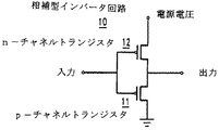
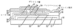
11 n−チャネルトランジスタ
12 p−チャネルトランジスタ
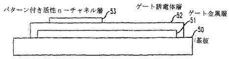
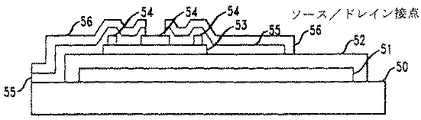
50 基板
51 ゲート金属層
52 ゲート誘電体層
53 パターン付き活性n−チャネル層
54 パターン付き分離層
55 n+a−Si層
56 ソース/ドレイン接点
57 ポリイミド層
58 α−6T層
59 ドレイン接点
60 パッシベーション膜
Claims (7)
- n−チャネルトランジスタとp−チャネルトランジスタが接続されて構成される製品において、
前記n−チャネルトランジスタ(11)は、無機薄膜トランジスタであり、
前記p−チャネルトランジスタ(12)は、有機薄膜トランジスタである
ことを特徴とするトランジスタからなる製品。 - 無機薄膜トランジスタは、アモルファスSi、多結晶Si、CdSe、TiO2、ZnO及びCu2Sからなる群から選択される金属からなる活性層からなり、
有機薄膜トランジスタは、
i) 2〜5個の炭素原子を介して結合された、オリゴ重合度が4以上8以下の、チオフェンのオリゴマー、
ii)2〜5個の炭素原子を介して結合された、3〜6個のチオフェン環と末端基としてチオフェンを有するビニレンと、チエニレンとの交互共オリゴマー、
iii)ベンゾ[1,2−b:4,5−b’]ジチオフェンの線状ダイマー及びトリマー、
iv)末端のチオフェンの4個又は5個の炭素原子上に置換基を有する前記i)、ii)及びiii)の何れかのオリゴマー、
v)テトラセン、ペンタセン及びこれらの末端置換誘導体、及び
vi)ポリマーマトリックス中のp,p’−ジアミノビフェニル複合体、
からなる群から選択される材料からなる活性層からなる請求項1の製品。 - 末端のチオフェンの4個又は5個の炭素原子上の置換基は炭素原子を1〜20個有するアルキル置換基である請求項2の製品。
- 前記第1及び第2のトランジスタは、相補型インバータ回路を形成するために、一緒に接続されて動作する請求項1の製品。
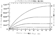
- 無機薄膜トランジスタはアモルファスシリコンからなる活性層からなる請求項1の製品。
- 有機薄膜トランジスタは、α−ヘキサチエニレンからなる活性層からなる請求項1の製品。
- 無機薄膜トランジスタはアモルファスシリコンからなる活性層からなる請求項6の製品。
Applications Claiming Priority (1)
| Application Number | Priority Date | Filing Date | Title |
|---|---|---|---|
| US08/587,426 US5625199A (en) | 1996-01-16 | 1996-01-16 | Article comprising complementary circuit with inorganic n-channel and organic p-channel thin film transistors |
Related Parent Applications (1)
| Application Number | Title | Priority Date | Filing Date |
|---|---|---|---|
| JP9003505A Division JPH09199732A (ja) | 1996-01-16 | 1997-01-13 | トランジスタからなる製品 |
Publications (1)
| Publication Number | Publication Date |
|---|---|
| JP2004228587A true JP2004228587A (ja) | 2004-08-12 |
Family
ID=24349767
Family Applications (2)
| Application Number | Title | Priority Date | Filing Date |
|---|---|---|---|
| JP9003505A Withdrawn JPH09199732A (ja) | 1996-01-16 | 1997-01-13 | トランジスタからなる製品 |
| JP2004048983A Pending JP2004228587A (ja) | 1996-01-16 | 2004-02-25 | トランジスタからなる製品 |
Family Applications Before (1)
| Application Number | Title | Priority Date | Filing Date |
|---|---|---|---|
| JP9003505A Withdrawn JPH09199732A (ja) | 1996-01-16 | 1997-01-13 | トランジスタからなる製品 |
Country Status (3)
| Country | Link |
|---|---|
| US (1) | US5625199A (ja) |
| EP (1) | EP0785578A3 (ja) |
| JP (2) | JPH09199732A (ja) |
Cited By (4)
| Publication number | Priority date | Publication date | Assignee | Title |
|---|---|---|---|---|
| JP2011129891A (ja) * | 2009-11-20 | 2011-06-30 | Semiconductor Energy Lab Co Ltd | 半導体装置 |
| KR101206659B1 (ko) | 2006-09-21 | 2012-11-30 | 삼성전자주식회사 | 올리고머 화합물을 포함하는 유기반도체 조성물, 이를포함하는 유기 반도체층 형성용 조성물, 이를 이용한유기반도체 박막 및 유기 전자소자 |
| US8643114B2 (en) | 2009-06-25 | 2014-02-04 | Seiko Epson Corporation | Semiconductor device and electronic apparatus |
| JP2025128126A (ja) * | 2009-05-29 | 2025-09-02 | 株式会社半導体エネルギー研究所 | 表示装置 |
Families Citing this family (135)
| Publication number | Priority date | Publication date | Assignee | Title |
|---|---|---|---|---|
| US6194167B1 (en) * | 1997-02-18 | 2001-02-27 | Washington State University Research Foundation | ω-3 fatty acid desaturase |
| US5981970A (en) * | 1997-03-25 | 1999-11-09 | International Business Machines Corporation | Thin-film field-effect transistor with organic semiconductor requiring low operating voltages |
| US5796121A (en) * | 1997-03-25 | 1998-08-18 | International Business Machines Corporation | Thin film transistors fabricated on plastic substrates |
| EP0968537B1 (en) * | 1997-08-22 | 2012-05-02 | Creator Technology B.V. | A method of manufacturing a field-effect transistor substantially consisting of organic materials |
| US6839158B2 (en) | 1997-08-28 | 2005-01-04 | E Ink Corporation | Encapsulated electrophoretic displays having a monolayer of capsules and materials and methods for making the same |
| US7242513B2 (en) * | 1997-08-28 | 2007-07-10 | E Ink Corporation | Encapsulated electrophoretic displays having a monolayer of capsules and materials and methods for making the same |
| EP1296280A1 (en) * | 1997-09-11 | 2003-03-26 | Precision Dynamics Corporation | Rf-id tag with integrated circuit consisting of organic materials |
| AU2002301482B2 (en) * | 1997-09-11 | 2004-06-10 | Precision Dynamics Corporation | Radio Frequency Identification Tag on Flexible Substrate |
| US5936259A (en) * | 1997-10-16 | 1999-08-10 | Lucent Technologies Inc. | Thin film transistor and organic semiconductor material thereof |
| US5998805A (en) * | 1997-12-11 | 1999-12-07 | Motorola, Inc. | Active matrix OED array with improved OED cathode |
| AU3552699A (en) | 1998-04-10 | 1999-11-01 | E-Ink Corporation | Electronic displays using organic-based field effect transistors |
| AU3987299A (en) | 1998-05-12 | 1999-11-29 | E-Ink Corporation | Microencapsulated electrophoretic electrostatically-addressed media for drawing device applications |
| EP1093663A2 (en) | 1998-06-19 | 2001-04-25 | Thin Film Electronics ASA | Integrated inorganic/organic complementary thin-film transistor circuit |
| US6215130B1 (en) * | 1998-08-20 | 2001-04-10 | Lucent Technologies Inc. | Thin film transistors |
| JP3276930B2 (ja) * | 1998-11-17 | 2002-04-22 | 科学技術振興事業団 | トランジスタ及び半導体装置 |
| US6384804B1 (en) | 1998-11-25 | 2002-05-07 | Lucent Techonologies Inc. | Display comprising organic smart pixels |
| US6842657B1 (en) * | 1999-04-09 | 2005-01-11 | E Ink Corporation | Reactive formation of dielectric layers and protection of organic layers in organic semiconductor device fabrication |
| US6498114B1 (en) | 1999-04-09 | 2002-12-24 | E Ink Corporation | Method for forming a patterned semiconductor film |
| US7030412B1 (en) | 1999-05-05 | 2006-04-18 | E Ink Corporation | Minimally-patterned semiconductor devices for display applications |
| GB9914489D0 (en) * | 1999-06-21 | 1999-08-25 | Univ Cambridge Tech | Transistors |
| AU7094400A (en) | 1999-08-31 | 2001-03-26 | E-Ink Corporation | A solvent annealing process for forming a thin semiconductor film with advantageous properties |
| EP1208603A1 (en) * | 1999-08-31 | 2002-05-29 | E Ink Corporation | Transistor for an electronically driven display |
| US6284562B1 (en) * | 1999-11-17 | 2001-09-04 | Agere Systems Guardian Corp. | Thin film transistors |
| US6197663B1 (en) | 1999-12-07 | 2001-03-06 | Lucent Technologies Inc. | Process for fabricating integrated circuit devices having thin film transistors |
| EP1136942A1 (de) * | 2000-03-22 | 2001-09-26 | Infineon Technologies AG | Schaltungsanordnung zum Schützen einer Schaltung gegen Analyse und Manipulation |
| KR100767233B1 (ko) | 2000-04-18 | 2007-10-17 | 이 잉크 코포레이션 | 박막 트랜지스터의 제조 공정 및 기판 |
| US7893435B2 (en) | 2000-04-18 | 2011-02-22 | E Ink Corporation | Flexible electronic circuits and displays including a backplane comprising a patterned metal foil having a plurality of apertures extending therethrough |
| KR20010097351A (ko) * | 2000-04-21 | 2001-11-08 | 구자홍 | 액티브 구동 유기 전계발광소자 제조방법 |
| US20020031602A1 (en) * | 2000-06-20 | 2002-03-14 | Chi Zhang | Thermal treatment of solution-processed organic electroactive layer in organic electronic device |
| US20020060321A1 (en) | 2000-07-14 | 2002-05-23 | Kazlas Peter T. | Minimally- patterned, thin-film semiconductor devices for display applications |
| DE10034873B4 (de) * | 2000-07-18 | 2005-10-13 | Pacifica Group Technologies Pty Ltd | Verfahren und Bremsanlage zum Regeln des Bremsvorgangs bei einem Kraftfahrzeug |
| WO2002015264A2 (de) | 2000-08-18 | 2002-02-21 | Siemens Aktiengesellschaft | Verkapseltes organisch-elektronisches bauteil, verfahren zu seiner herstellung und seine verwendung |
| US20040029310A1 (en) * | 2000-08-18 | 2004-02-12 | Adoft Bernds | Organic field-effect transistor (ofet), a production method therefor, an integrated circut constructed from the same and their uses |
| DE10043204A1 (de) * | 2000-09-01 | 2002-04-04 | Siemens Ag | Organischer Feld-Effekt-Transistor, Verfahren zur Strukturierung eines OFETs und integrierte Schaltung |
| DE10044842A1 (de) * | 2000-09-11 | 2002-04-04 | Siemens Ag | Organischer Gleichrichter, Schaltung, RFID-Tag und Verwendung eines organischen Gleichrichters |
| DE10045192A1 (de) * | 2000-09-13 | 2002-04-04 | Siemens Ag | Organischer Datenspeicher, RFID-Tag mit organischem Datenspeicher, Verwendung eines organischen Datenspeichers |
| EP1323195A1 (de) * | 2000-09-22 | 2003-07-02 | Siemens Aktiengesellschaft | Elektrode und/oder leiterbahn für organische bauelemente und herstellungsverfahren dazu |
| DE10061299A1 (de) * | 2000-12-08 | 2002-06-27 | Siemens Ag | Vorrichtung zur Feststellung und/oder Weiterleitung zumindest eines Umwelteinflusses, Herstellungsverfahren und Verwendung dazu |
| DE10061297C2 (de) * | 2000-12-08 | 2003-05-28 | Siemens Ag | Verfahren zur Sturkturierung eines OFETs |
| DE10063721A1 (de) * | 2000-12-20 | 2002-07-11 | Merck Patent Gmbh | Organischer Halbleiter, Herstellungsverfahren dazu und Verwendungen |
| DE10105914C1 (de) | 2001-02-09 | 2002-10-10 | Siemens Ag | Organischer Feldeffekt-Transistor mit fotostrukturiertem Gate-Dielektrikum und ein Verfahren zu dessen Erzeugung |
| US6692662B2 (en) * | 2001-02-16 | 2004-02-17 | Elecon, Inc. | Compositions produced by solvent exchange methods and uses thereof |
| DE10126860C2 (de) * | 2001-06-01 | 2003-05-28 | Siemens Ag | Organischer Feldeffekt-Transistor, Verfahren zu seiner Herstellung und Verwendung zum Aufbau integrierter Schaltungen |
| US6967640B2 (en) * | 2001-07-27 | 2005-11-22 | E Ink Corporation | Microencapsulated electrophoretic display with integrated driver |
| US6433359B1 (en) | 2001-09-06 | 2002-08-13 | 3M Innovative Properties Company | Surface modifying layers for organic thin film transistors |
| DE10151036A1 (de) * | 2001-10-16 | 2003-05-08 | Siemens Ag | Isolator für ein organisches Elektronikbauteil |
| DE10151440C1 (de) * | 2001-10-18 | 2003-02-06 | Siemens Ag | Organisches Elektronikbauteil, Verfahren zu seiner Herstellung und seine Verwendung |
| US6946676B2 (en) * | 2001-11-05 | 2005-09-20 | 3M Innovative Properties Company | Organic thin film transistor with polymeric interface |
| US6617609B2 (en) | 2001-11-05 | 2003-09-09 | 3M Innovative Properties Company | Organic thin film transistor with siloxane polymer interface |
| DE10160732A1 (de) * | 2001-12-11 | 2003-06-26 | Siemens Ag | Organischer Feld-Effekt-Transistor mit verschobener Schwellwertspannung und Verwendung dazu |
| US6620657B2 (en) * | 2002-01-15 | 2003-09-16 | International Business Machines Corporation | Method of forming a planar polymer transistor using substrate bonding techniques |
| US6900851B2 (en) | 2002-02-08 | 2005-05-31 | E Ink Corporation | Electro-optic displays and optical systems for addressing such displays |
| US6768132B2 (en) | 2002-03-07 | 2004-07-27 | 3M Innovative Properties Company | Surface modified organic thin film transistors |
| DE10212639A1 (de) * | 2002-03-21 | 2003-10-16 | Siemens Ag | Vorrichtung und Verfahren zur Laserstrukturierung von Funktionspolymeren und Verwendungen |
| DE10212640B4 (de) * | 2002-03-21 | 2004-02-05 | Siemens Ag | Logische Bauteile aus organischen Feldeffekttransistoren |
| US6667215B2 (en) | 2002-05-02 | 2003-12-23 | 3M Innovative Properties | Method of making transistors |
| US7339187B2 (en) * | 2002-05-21 | 2008-03-04 | State Of Oregon Acting By And Through The Oregon State Board Of Higher Education On Behalf Of Oregon State University | Transistor structures |
| US7189992B2 (en) * | 2002-05-21 | 2007-03-13 | State Of Oregon Acting By And Through The Oregon State Board Of Higher Education On Behalf Of Oregon State University | Transistor structures having a transparent channel |
| DE10226370B4 (de) * | 2002-06-13 | 2008-12-11 | Polyic Gmbh & Co. Kg | Substrat für ein elektronisches Bauteil, Verwendung des Substrates, Verfahren zur Erhöhung der Ladungsträgermobilität und Organischer Feld-Effekt Transistor (OFET) |
| JP4136482B2 (ja) * | 2002-06-20 | 2008-08-20 | キヤノン株式会社 | 有機半導体素子、その製造方法および有機半導体装置 |
| WO2004017439A2 (de) | 2002-07-29 | 2004-02-26 | Siemens Aktiengesellschaft | Elektronisches bauteil mit vorwiegend organischen funktionsmaterialien und herstellungsverfahren dazu |
| DE50309888D1 (de) * | 2002-08-08 | 2008-07-03 | Polyic Gmbh & Co Kg | Elektronisches gerät |
| ATE355566T1 (de) | 2002-08-23 | 2006-03-15 | Polyic Gmbh & Co Kg | Organisches bauelement zum überspannungsschutz und dazugehörige schaltung |
| US6852996B2 (en) * | 2002-09-25 | 2005-02-08 | Stmicroelectronics, Inc. | Organic semiconductor sensor device |
| US7067843B2 (en) * | 2002-10-11 | 2006-06-27 | E. I. Du Pont De Nemours And Company | Transparent oxide semiconductor thin film transistors |
| JP2004152958A (ja) * | 2002-10-30 | 2004-05-27 | Pioneer Electronic Corp | 有機半導体装置 |
| US20060118778A1 (en) * | 2002-11-05 | 2006-06-08 | Wolfgang Clemens | Organic electronic component with high-resolution structuring and method for the production thereof |
| DE10253154A1 (de) | 2002-11-14 | 2004-05-27 | Siemens Ag | Messgerät zur Bestimmung eines Analyten in einer Flüssigkeitsprobe |
| US7442954B2 (en) | 2002-11-19 | 2008-10-28 | Polyic Gmbh & Co. Kg | Organic electronic component comprising a patterned, semi-conducting functional layer and a method for producing said component |
| KR100572926B1 (ko) * | 2002-12-26 | 2006-04-24 | 삼성전자주식회사 | 폴리티에닐티아졸 유도체 및 이를 이용한 유기박막트랜지스터 |
| WO2004063806A1 (de) * | 2003-01-09 | 2004-07-29 | Polyic Gmbh & Co. Kg | Platine oder substrat für ein organisches elektronikgerät, sowie verwendung dazu |
| DE10302149A1 (de) | 2003-01-21 | 2005-08-25 | Siemens Ag | Verwendung leitfähiger Carbon-black/Graphit-Mischungen für die Herstellung von low-cost Elektronik |
| JP2006518938A (ja) * | 2003-01-28 | 2006-08-17 | コーニンクレッカ フィリップス エレクトロニクス エヌ ヴィ | 電子装置 |
| US7224118B2 (en) * | 2003-06-17 | 2007-05-29 | Semiconductor Energy Laboratory Co., Ltd. | Display device and electronic apparatus having a wiring connected to a counter electrode via an opening portion in an insulating layer that surrounds a pixel electrode |
| JP4593179B2 (ja) * | 2003-06-17 | 2010-12-08 | 株式会社半導体エネルギー研究所 | 表示装置 |
| GB2403848A (en) * | 2003-07-08 | 2005-01-12 | Seiko Epson Corp | Semiconductor device |
| CN1823425A (zh) * | 2003-07-10 | 2006-08-23 | 松下电器产业株式会社 | 有机薄膜晶体管及其制造方法、以及使用了它的有源矩阵型显示器和无线识别标签 |
| US7354127B2 (en) * | 2003-07-16 | 2008-04-08 | Seiko Epson Corporation | Method for forming ejection-test pattern, method for testing ejection, printing apparatus, computer-readable medium, and printing system |
| DE10338277A1 (de) * | 2003-08-20 | 2005-03-17 | Siemens Ag | Organischer Kondensator mit spannungsgesteuerter Kapazität |
| DE10339036A1 (de) | 2003-08-25 | 2005-03-31 | Siemens Ag | Organisches elektronisches Bauteil mit hochaufgelöster Strukturierung und Herstellungsverfahren dazu |
| DE10340643B4 (de) * | 2003-09-03 | 2009-04-16 | Polyic Gmbh & Co. Kg | Druckverfahren zur Herstellung einer Doppelschicht für Polymerelektronik-Schaltungen, sowie dadurch hergestelltes elektronisches Bauelement mit Doppelschicht |
| DE10340644B4 (de) * | 2003-09-03 | 2010-10-07 | Polyic Gmbh & Co. Kg | Mechanische Steuerelemente für organische Polymerelektronik |
| US7122828B2 (en) * | 2003-09-24 | 2006-10-17 | Lucent Technologies, Inc. | Semiconductor devices having regions of induced high and low conductivity, and methods of making the same |
| DE602004024629D1 (de) * | 2003-10-15 | 2010-01-28 | Merck Patent Gmbh | Polybenzodithiophene |
| US7045470B2 (en) * | 2003-11-04 | 2006-05-16 | Lucent Technologies Inc. | Methods of making thin dielectric layers on substrates |
| US8450723B2 (en) * | 2003-11-04 | 2013-05-28 | Alcatel Lucent | Apparatus having an aromatic dielectric and an aromatic organic semiconductor including an alkyl chain |
| US7115900B2 (en) * | 2003-11-26 | 2006-10-03 | Lucent Technologies Inc. | Devices having patterned regions of polycrystalline organic semiconductors, and methods of making the same |
| KR101007787B1 (ko) * | 2003-12-08 | 2011-01-14 | 삼성전자주식회사 | 퀴녹살린환을 주쇄에 포함하는 유기박막 트랜지스터용유기반도체 고분자 |
| KR100982122B1 (ko) * | 2003-12-30 | 2010-09-14 | 엘지디스플레이 주식회사 | 수평 전계 인가형 박막 트랜지스터 기판의 불량 화소암점화 방법 |
| DE102004002024A1 (de) * | 2004-01-14 | 2005-08-11 | Siemens Ag | Organischer Transistor mit selbstjustierender Gate-Elektrode und Verfahren zu dessen Herstellung |
| US7385220B2 (en) * | 2004-04-12 | 2008-06-10 | Lucent Technologies Inc. | Fiber having dielectric polymeric layer on electrically conductive surface |
| DE102004040831A1 (de) * | 2004-08-23 | 2006-03-09 | Polyic Gmbh & Co. Kg | Funketikettfähige Umverpackung |
| WO2006022017A1 (ja) * | 2004-08-27 | 2006-03-02 | Fuji Electric Holdings Co., Ltd. | 論理回路 |
| US7298084B2 (en) * | 2004-11-02 | 2007-11-20 | 3M Innovative Properties Company | Methods and displays utilizing integrated zinc oxide row and column drivers in conjunction with organic light emitting diodes |
| EP2453481B1 (en) * | 2004-11-10 | 2017-01-11 | Canon Kabushiki Kaisha | Field effect transistor with amorphous oxide |
| DE102004059465A1 (de) * | 2004-12-10 | 2006-06-14 | Polyic Gmbh & Co. Kg | Erkennungssystem |
| DE102004059464A1 (de) * | 2004-12-10 | 2006-06-29 | Polyic Gmbh & Co. Kg | Elektronikbauteil mit Modulator |
| DE102004063435A1 (de) | 2004-12-23 | 2006-07-27 | Polyic Gmbh & Co. Kg | Organischer Gleichrichter |
| DE102005009819A1 (de) | 2005-03-01 | 2006-09-07 | Polyic Gmbh & Co. Kg | Elektronikbaugruppe |
| DE102005009820A1 (de) * | 2005-03-01 | 2006-09-07 | Polyic Gmbh & Co. Kg | Elektronikbaugruppe mit organischen Logik-Schaltelementen |
| US7371605B2 (en) * | 2005-03-25 | 2008-05-13 | Lucent Technologies Inc. | Active organic semiconductor devices and methods for making the same |
| DE102005017655B4 (de) * | 2005-04-15 | 2008-12-11 | Polyic Gmbh & Co. Kg | Mehrschichtiger Verbundkörper mit elektronischer Funktion |
| DE102005031448A1 (de) | 2005-07-04 | 2007-01-11 | Polyic Gmbh & Co. Kg | Aktivierbare optische Schicht |
| DE102005035590A1 (de) * | 2005-07-29 | 2007-02-01 | Polyic Gmbh & Co. Kg | Elektronisches Bauelement |
| DE102005035589A1 (de) | 2005-07-29 | 2007-02-01 | Polyic Gmbh & Co. Kg | Verfahren zur Herstellung eines elektronischen Bauelements |
| DE102005042166A1 (de) * | 2005-09-06 | 2007-03-15 | Polyic Gmbh & Co.Kg | Organisches Bauelement und ein solches umfassende elektrische Schaltung |
| DE102005044306A1 (de) * | 2005-09-16 | 2007-03-22 | Polyic Gmbh & Co. Kg | Elektronische Schaltung und Verfahren zur Herstellung einer solchen |
| EP3614442A3 (en) * | 2005-09-29 | 2020-03-25 | Semiconductor Energy Laboratory Co., Ltd. | Semiconductor device having oxide semiconductor layer and manufactoring method thereof |
| US7397072B2 (en) * | 2005-12-01 | 2008-07-08 | Board Of Regents, The University Of Texas System | Structure for and method of using a four terminal hybrid silicon/organic field effect sensor device |
| US20070215863A1 (en) * | 2006-03-15 | 2007-09-20 | Lucent Technologies Inc. | Fabricating apparatus with doped organic semiconductors |
| DE102006013605A1 (de) * | 2006-03-22 | 2007-10-11 | Polyic Gmbh & Co. Kg | Verfahren zum Programmieren einer elektronischen Schaltung sowie elektronische Schaltung |
| KR101314931B1 (ko) * | 2006-10-30 | 2013-10-04 | 삼성전자주식회사 | 유기 고분자 반도체, 이의 제조방법 및 이를 이용한 양극성 유기 박막 트랜지스터 |
| KR101430260B1 (ko) * | 2007-01-24 | 2014-08-14 | 삼성전자주식회사 | 티아졸 함유 유기반도체 고분자, 이의 제조방법 및 이를이용한 유기박막트랜지스터 |
| WO2008099863A1 (ja) * | 2007-02-16 | 2008-08-21 | Idemitsu Kosan Co., Ltd. | 半導体,半導体装置及び相補型トランジスタ回路装置 |
| US8129714B2 (en) | 2007-02-16 | 2012-03-06 | Idemitsu Kosan Co., Ltd. | Semiconductor, semiconductor device, complementary transistor circuit device |
| US7768042B2 (en) * | 2007-03-29 | 2010-08-03 | Korea Advanced Institute Of Science And Technology | Thin film transistor including titanium oxides as active layer and method of manufacturing the same |
| KR20080101229A (ko) * | 2007-05-16 | 2008-11-21 | 삼성전자주식회사 | 액정성을 가지는 유기반도체 고분자, 이의 제조방법 및이를 이용한 유기박막트랜지스터 |
| JPWO2009028453A1 (ja) * | 2007-08-31 | 2010-12-02 | コニカミノルタホールディングス株式会社 | 薄膜トランジスタ |
| KR101377924B1 (ko) | 2007-11-08 | 2014-03-25 | 삼성전자주식회사 | 페닐렌 비닐렌-올리고아릴렌 비닐렌 교호공중합체, 이의제조방법 및 이를 포함하는 유기박막 트랜지스터 |
| KR101377842B1 (ko) * | 2007-11-08 | 2014-03-25 | 삼성전자주식회사 | 페닐렌 비닐렌-바이아릴렌 비닐렌 교호공중합체, 이의제조방법 및 이를 포함하는 유기박막 트랜지스터 |
| KR101450137B1 (ko) * | 2008-01-25 | 2014-10-13 | 삼성전자주식회사 | 유기반도체용 공중합체 및 이를 이용한 유기박막트랜지스터 및 유기 전자소자 |
| US7821000B2 (en) * | 2008-02-01 | 2010-10-26 | Alcatel-Lucent Usa Inc. | Method of doping organic semiconductors |
| WO2009117438A2 (en) * | 2008-03-20 | 2009-09-24 | Applied Materials, Inc. | Process to make metal oxide thin film transistor array with etch stopping layer |
| KR101490112B1 (ko) * | 2008-03-28 | 2015-02-05 | 삼성전자주식회사 | 인버터 및 그를 포함하는 논리회로 |
| DE102008026216B4 (de) | 2008-05-30 | 2010-07-29 | Polyic Gmbh & Co. Kg | Elektronische Schaltung |
| US8272458B2 (en) * | 2008-06-12 | 2012-09-25 | Nackerud Alan L | Drill bit with replaceable blade members |
| US8258511B2 (en) | 2008-07-02 | 2012-09-04 | Applied Materials, Inc. | Thin film transistors using multiple active channel layers |
| JP2010034343A (ja) * | 2008-07-30 | 2010-02-12 | Sumitomo Chemical Co Ltd | 半導体装置の製造方法および半導体装置 |
| US20110031489A1 (en) * | 2009-06-19 | 2011-02-10 | The Regents Of The University Of Michigan | COMPLEMENTARY THIN FILM ELECTRONICS BASED ON ZnO/ZnTe |
| US8212243B2 (en) | 2010-01-22 | 2012-07-03 | Eastman Kodak Company | Organic semiconducting compositions and N-type semiconductor devices |
| CN102544051A (zh) * | 2011-08-31 | 2012-07-04 | 上海大学 | 有机互补反相器及其制备方法 |
| CN103268918B (zh) * | 2012-06-29 | 2016-06-29 | 上海天马微电子有限公司 | 双极性薄膜晶体管及其制造方法 |
| CN103000632B (zh) * | 2012-12-12 | 2015-08-05 | 京东方科技集团股份有限公司 | 一种cmos电路结构、其制备方法及显示装置 |
| CN105742308B (zh) * | 2016-02-29 | 2019-09-13 | 深圳市华星光电技术有限公司 | 互补型薄膜晶体管及其制造方法 |
| CN106252362B (zh) * | 2016-08-31 | 2019-07-12 | 深圳市华星光电技术有限公司 | 一种阵列基板及其制备方法 |
Family Cites Families (4)
| Publication number | Priority date | Publication date | Assignee | Title |
|---|---|---|---|---|
| JPH01259563A (ja) * | 1988-04-08 | 1989-10-17 | Mitsubishi Electric Corp | 電界効果型トランジスタ |
| FR2664430B1 (fr) * | 1990-07-04 | 1992-09-18 | Centre Nat Rech Scient | Transistor a effet de champ en couche mince de structure mis, dont l'isolant et le semiconducteur sont realises en materiaux organiques. |
| US5298455A (en) * | 1991-01-30 | 1994-03-29 | Tdk Corporation | Method for producing a non-single crystal semiconductor device |
| US5612228A (en) * | 1996-04-24 | 1997-03-18 | Motorola | Method of making CMOS with organic and inorganic semiconducting region |
-
1996
- 1996-01-16 US US08/587,426 patent/US5625199A/en not_active Expired - Lifetime
-
1997
- 1997-01-07 EP EP97300063A patent/EP0785578A3/en not_active Withdrawn
- 1997-01-13 JP JP9003505A patent/JPH09199732A/ja not_active Withdrawn
-
2004
- 2004-02-25 JP JP2004048983A patent/JP2004228587A/ja active Pending
Cited By (8)
| Publication number | Priority date | Publication date | Assignee | Title |
|---|---|---|---|---|
| KR101206659B1 (ko) | 2006-09-21 | 2012-11-30 | 삼성전자주식회사 | 올리고머 화합물을 포함하는 유기반도체 조성물, 이를포함하는 유기 반도체층 형성용 조성물, 이를 이용한유기반도체 박막 및 유기 전자소자 |
| JP2025128126A (ja) * | 2009-05-29 | 2025-09-02 | 株式会社半導体エネルギー研究所 | 表示装置 |
| US8643114B2 (en) | 2009-06-25 | 2014-02-04 | Seiko Epson Corporation | Semiconductor device and electronic apparatus |
| JP2011129891A (ja) * | 2009-11-20 | 2011-06-30 | Semiconductor Energy Lab Co Ltd | 半導体装置 |
| US8892158B2 (en) | 2009-11-20 | 2014-11-18 | Semiconductor Energy Laboratory Co., Ltd. | Semiconductor device |
| US9373643B2 (en) | 2009-11-20 | 2016-06-21 | Semiconductor Energy Laboratory Co., Ltd. | Semiconductor device |
| US9741867B2 (en) | 2009-11-20 | 2017-08-22 | Semiconductor Energy Laboratory Co., Ltd. | Semiconductor device |
| US10121904B2 (en) | 2009-11-20 | 2018-11-06 | Semiconductor Energy Laboratory Co., Ltd. | Semiconductor device |
Also Published As
| Publication number | Publication date |
|---|---|
| JPH09199732A (ja) | 1997-07-31 |
| EP0785578A3 (en) | 1998-04-22 |
| US5625199A (en) | 1997-04-29 |
| EP0785578A2 (en) | 1997-07-23 |
Similar Documents
| Publication | Publication Date | Title |
|---|---|---|
| JP2004228587A (ja) | トランジスタからなる製品 | |
| CA2334862C (en) | An integrated inorganic/organic complementary thin-film transistor circuit and a method for its production | |
| US6232157B1 (en) | Thin film transistors | |
| Klauk et al. | Fast organic thin-film transistor circuits | |
| Halik et al. | High-mobility organic thin-film transistors based on α, α′-didecyloligothiophenes | |
| Chabinyc et al. | Lamination method for the study of interfaces in polymeric thin film transistors | |
| JP4166485B2 (ja) | 集積回路薄膜トランジスタデバイスの製造方法 | |
| US6284562B1 (en) | Thin film transistors | |
| US6847048B2 (en) | Organic thin film transistor (OTFT) | |
| Zschieschang et al. | Microcontact-printed self-assembled monolayers as ultrathin gate dielectrics in organic thin-film transistors and complementary circuits | |
| US8389992B2 (en) | Organic thin film transistor array panel and manufacturing method thereof | |
| EP1629546B1 (en) | A field effect transistor arrangement and method of manufacturing a field effect transistor arrangement | |
| TW200301941A (en) | Planar polymer transistor | |
| JP2004266267A (ja) | 保護層を含む有機半導体電界効果トランジスタ及びその製造方法 | |
| US20050221530A1 (en) | Method for enhancing electrical characteristics of organic electronic devices | |
| Zhao et al. | Wafer‐scale organic complementary inverters fabricated with self‐assembled monolayer field‐effect transistors | |
| Tatemichi et al. | Low‐voltage, high‐gain, and high‐mobility organic complementary inverters based on N, N′‐ditridecyl‐3, 4, 9, 10‐perylenetetracarboxylic diimide and pentacene | |
| US20050287719A1 (en) | Organic thin film transistor array panel and manufacturing method thereof | |
| US20060220007A1 (en) | Acene compounds having a single terminal fused thiophene as semiconductor materials for thin film transistors and methods of making the same | |
| US7259392B2 (en) | Organic thin film transistor array panel and manufacturing method thereof | |
| Klauk et al. | Polymer gate dielectric pentacene TFTs and circuits on flexible substrates | |
| Kim et al. | P‐45: Gate Driver Circuit with Pre‐bootstrapping Using Organic TFTs | |
| CN1790681B (zh) | 有机薄膜晶体管阵列面板及其制造方法 | |
| CN100505186C (zh) | 垂直薄膜晶体管的制造方法 | |
| EP2259354A2 (en) | Perylene imide/diimide based organic field effect transistors-OFETs and a method of producing the same |
Legal Events
| Date | Code | Title | Description |
|---|---|---|---|
| A131 | Notification of reasons for refusal |
Free format text: JAPANESE INTERMEDIATE CODE: A131 Effective date: 20070221 |
|
| A601 | Written request for extension of time |
Free format text: JAPANESE INTERMEDIATE CODE: A601 Effective date: 20070521 |
|
| A602 | Written permission of extension of time |
Free format text: JAPANESE INTERMEDIATE CODE: A602 Effective date: 20070524 |
|
| A521 | Request for written amendment filed |
Free format text: JAPANESE INTERMEDIATE CODE: A523 Effective date: 20070821 |
|
| A02 | Decision of refusal |
Free format text: JAPANESE INTERMEDIATE CODE: A02 Effective date: 20080218 |