WO2012169209A1 - 半導体デバイス、半導体基板、半導体基板の製造方法および半導体デバイスの製造方法 - Google Patents
半導体デバイス、半導体基板、半導体基板の製造方法および半導体デバイスの製造方法 Download PDFInfo
- Publication number
- WO2012169209A1 WO2012169209A1 PCT/JP2012/003769 JP2012003769W WO2012169209A1 WO 2012169209 A1 WO2012169209 A1 WO 2012169209A1 JP 2012003769 W JP2012003769 W JP 2012003769W WO 2012169209 A1 WO2012169209 A1 WO 2012169209A1
- Authority
- WO
- WIPO (PCT)
- Prior art keywords
- semiconductor crystal
- crystal layer
- layer
- semiconductor
- substrate
- Prior art date
- Legal status (The legal status is an assumption and is not a legal conclusion. Google has not performed a legal analysis and makes no representation as to the accuracy of the status listed.)
- Ceased
Links
Images






Classifications
-
- H—ELECTRICITY
- H10—SEMICONDUCTOR DEVICES; ELECTRIC SOLID-STATE DEVICES NOT OTHERWISE PROVIDED FOR
- H10D—INORGANIC ELECTRIC SEMICONDUCTOR DEVICES
- H10D84/00—Integrated devices formed in or on semiconductor substrates that comprise only semiconducting layers, e.g. on Si wafers or on GaAs-on-Si wafers
- H10D84/01—Manufacture or treatment
- H10D84/0123—Integrating together multiple components covered by H10D12/00 or H10D30/00, e.g. integrating multiple IGBTs
- H10D84/0126—Integrating together multiple components covered by H10D12/00 or H10D30/00, e.g. integrating multiple IGBTs the components including insulated gates, e.g. IGFETs
- H10D84/0165—Integrating together multiple components covered by H10D12/00 or H10D30/00, e.g. integrating multiple IGBTs the components including insulated gates, e.g. IGFETs the components including complementary IGFETs, e.g. CMOS devices
-
- H—ELECTRICITY
- H10—SEMICONDUCTOR DEVICES; ELECTRIC SOLID-STATE DEVICES NOT OTHERWISE PROVIDED FOR
- H10D—INORGANIC ELECTRIC SEMICONDUCTOR DEVICES
- H10D30/00—Field-effect transistors [FET]
- H10D30/60—Insulated-gate field-effect transistors [IGFET]
- H10D30/67—Thin-film transistors [TFT]
- H10D30/674—Thin-film transistors [TFT] characterised by the active materials
- H10D30/6741—Group IV materials, e.g. germanium or silicon carbide
-
- H—ELECTRICITY
- H10—SEMICONDUCTOR DEVICES; ELECTRIC SOLID-STATE DEVICES NOT OTHERWISE PROVIDED FOR
- H10D—INORGANIC ELECTRIC SEMICONDUCTOR DEVICES
- H10D64/00—Electrodes of devices having potential barriers
- H10D64/01—Manufacture or treatment
- H10D64/011—Manufacture or treatment of electrodes ohmically coupled to a semiconductor
-
- H—ELECTRICITY
- H10—SEMICONDUCTOR DEVICES; ELECTRIC SOLID-STATE DEVICES NOT OTHERWISE PROVIDED FOR
- H10D—INORGANIC ELECTRIC SEMICONDUCTOR DEVICES
- H10D64/00—Electrodes of devices having potential barriers
- H10D64/01—Manufacture or treatment
- H10D64/011—Manufacture or treatment of electrodes ohmically coupled to a semiconductor
- H10D64/0111—Manufacture or treatment of electrodes ohmically coupled to a semiconductor to Group IV semiconductors
- H10D64/0112—Manufacture or treatment of electrodes ohmically coupled to a semiconductor to Group IV semiconductors using conductive layers comprising silicides
-
- H—ELECTRICITY
- H10—SEMICONDUCTOR DEVICES; ELECTRIC SOLID-STATE DEVICES NOT OTHERWISE PROVIDED FOR
- H10D—INORGANIC ELECTRIC SEMICONDUCTOR DEVICES
- H10D84/00—Integrated devices formed in or on semiconductor substrates that comprise only semiconducting layers, e.g. on Si wafers or on GaAs-on-Si wafers
- H10D84/01—Manufacture or treatment
- H10D84/0123—Integrating together multiple components covered by H10D12/00 or H10D30/00, e.g. integrating multiple IGBTs
- H10D84/0126—Integrating together multiple components covered by H10D12/00 or H10D30/00, e.g. integrating multiple IGBTs the components including insulated gates, e.g. IGFETs
- H10D84/0165—Integrating together multiple components covered by H10D12/00 or H10D30/00, e.g. integrating multiple IGBTs the components including insulated gates, e.g. IGFETs the components including complementary IGFETs, e.g. CMOS devices
- H10D84/0167—Manufacturing their channels
-
- H—ELECTRICITY
- H10—SEMICONDUCTOR DEVICES; ELECTRIC SOLID-STATE DEVICES NOT OTHERWISE PROVIDED FOR
- H10D—INORGANIC ELECTRIC SEMICONDUCTOR DEVICES
- H10D84/00—Integrated devices formed in or on semiconductor substrates that comprise only semiconducting layers, e.g. on Si wafers or on GaAs-on-Si wafers
- H10D84/01—Manufacture or treatment
- H10D84/02—Manufacture or treatment characterised by using material-based technologies
- H10D84/03—Manufacture or treatment characterised by using material-based technologies using Group IV technology, e.g. silicon technology or silicon-carbide [SiC] technology
- H10D84/038—Manufacture or treatment characterised by using material-based technologies using Group IV technology, e.g. silicon technology or silicon-carbide [SiC] technology using silicon technology, e.g. SiGe
-
- H—ELECTRICITY
- H10—SEMICONDUCTOR DEVICES; ELECTRIC SOLID-STATE DEVICES NOT OTHERWISE PROVIDED FOR
- H10D—INORGANIC ELECTRIC SEMICONDUCTOR DEVICES
- H10D84/00—Integrated devices formed in or on semiconductor substrates that comprise only semiconducting layers, e.g. on Si wafers or on GaAs-on-Si wafers
- H10D84/01—Manufacture or treatment
- H10D84/02—Manufacture or treatment characterised by using material-based technologies
- H10D84/05—Manufacture or treatment characterised by using material-based technologies using Group III-V technology
-
- H—ELECTRICITY
- H10—SEMICONDUCTOR DEVICES; ELECTRIC SOLID-STATE DEVICES NOT OTHERWISE PROVIDED FOR
- H10D—INORGANIC ELECTRIC SEMICONDUCTOR DEVICES
- H10D84/00—Integrated devices formed in or on semiconductor substrates that comprise only semiconducting layers, e.g. on Si wafers or on GaAs-on-Si wafers
- H10D84/01—Manufacture or treatment
- H10D84/02—Manufacture or treatment characterised by using material-based technologies
- H10D84/08—Manufacture or treatment characterised by using material-based technologies using combinations of technologies, e.g. using both Si and SiC technologies or using both Si and Group III-V technologies
-
- H—ELECTRICITY
- H10—SEMICONDUCTOR DEVICES; ELECTRIC SOLID-STATE DEVICES NOT OTHERWISE PROVIDED FOR
- H10D—INORGANIC ELECTRIC SEMICONDUCTOR DEVICES
- H10D84/00—Integrated devices formed in or on semiconductor substrates that comprise only semiconducting layers, e.g. on Si wafers or on GaAs-on-Si wafers
- H10D84/80—Integrated devices formed in or on semiconductor substrates that comprise only semiconducting layers, e.g. on Si wafers or on GaAs-on-Si wafers characterised by the integration of at least one component covered by groups H10D12/00 or H10D30/00, e.g. integration of IGFETs
- H10D84/82—Integrated devices formed in or on semiconductor substrates that comprise only semiconducting layers, e.g. on Si wafers or on GaAs-on-Si wafers characterised by the integration of at least one component covered by groups H10D12/00 or H10D30/00, e.g. integration of IGFETs of only field-effect components
- H10D84/83—Integrated devices formed in or on semiconductor substrates that comprise only semiconducting layers, e.g. on Si wafers or on GaAs-on-Si wafers characterised by the integration of at least one component covered by groups H10D12/00 or H10D30/00, e.g. integration of IGFETs of only field-effect components of only insulated-gate FETs [IGFET]
- H10D84/85—Complementary IGFETs, e.g. CMOS
-
- H—ELECTRICITY
- H10—SEMICONDUCTOR DEVICES; ELECTRIC SOLID-STATE DEVICES NOT OTHERWISE PROVIDED FOR
- H10D—INORGANIC ELECTRIC SEMICONDUCTOR DEVICES
- H10D84/00—Integrated devices formed in or on semiconductor substrates that comprise only semiconducting layers, e.g. on Si wafers or on GaAs-on-Si wafers
- H10D84/80—Integrated devices formed in or on semiconductor substrates that comprise only semiconducting layers, e.g. on Si wafers or on GaAs-on-Si wafers characterised by the integration of at least one component covered by groups H10D12/00 or H10D30/00, e.g. integration of IGFETs
- H10D84/82—Integrated devices formed in or on semiconductor substrates that comprise only semiconducting layers, e.g. on Si wafers or on GaAs-on-Si wafers characterised by the integration of at least one component covered by groups H10D12/00 or H10D30/00, e.g. integration of IGFETs of only field-effect components
- H10D84/83—Integrated devices formed in or on semiconductor substrates that comprise only semiconducting layers, e.g. on Si wafers or on GaAs-on-Si wafers characterised by the integration of at least one component covered by groups H10D12/00 or H10D30/00, e.g. integration of IGFETs of only field-effect components of only insulated-gate FETs [IGFET]
- H10D84/85—Complementary IGFETs, e.g. CMOS
- H10D84/856—Complementary IGFETs, e.g. CMOS the complementary IGFETs having different architectures than each other, e.g. high-voltage and low-voltage CMOS
-
- H—ELECTRICITY
- H10—SEMICONDUCTOR DEVICES; ELECTRIC SOLID-STATE DEVICES NOT OTHERWISE PROVIDED FOR
- H10D—INORGANIC ELECTRIC SEMICONDUCTOR DEVICES
- H10D84/00—Integrated devices formed in or on semiconductor substrates that comprise only semiconducting layers, e.g. on Si wafers or on GaAs-on-Si wafers
- H10D84/80—Integrated devices formed in or on semiconductor substrates that comprise only semiconducting layers, e.g. on Si wafers or on GaAs-on-Si wafers characterised by the integration of at least one component covered by groups H10D12/00 or H10D30/00, e.g. integration of IGFETs
- H10D84/86—Integrated devices formed in or on semiconductor substrates that comprise only semiconducting layers, e.g. on Si wafers or on GaAs-on-Si wafers characterised by the integration of at least one component covered by groups H10D12/00 or H10D30/00, e.g. integration of IGFETs of Schottky-barrier gate FETs
-
- H—ELECTRICITY
- H10—SEMICONDUCTOR DEVICES; ELECTRIC SOLID-STATE DEVICES NOT OTHERWISE PROVIDED FOR
- H10D—INORGANIC ELECTRIC SEMICONDUCTOR DEVICES
- H10D86/00—Integrated devices formed in or on insulating or conducting substrates, e.g. formed in silicon-on-insulator [SOI] substrates or on stainless steel or glass substrates
- H10D86/01—Manufacture or treatment
-
- H—ELECTRICITY
- H10—SEMICONDUCTOR DEVICES; ELECTRIC SOLID-STATE DEVICES NOT OTHERWISE PROVIDED FOR
- H10D—INORGANIC ELECTRIC SEMICONDUCTOR DEVICES
- H10D86/00—Integrated devices formed in or on insulating or conducting substrates, e.g. formed in silicon-on-insulator [SOI] substrates or on stainless steel or glass substrates
- H10D86/201—Integrated devices formed in or on insulating or conducting substrates, e.g. formed in silicon-on-insulator [SOI] substrates or on stainless steel or glass substrates the substrates comprising an insulating layer on a semiconductor body, e.g. SOI
-
- H—ELECTRICITY
- H10—SEMICONDUCTOR DEVICES; ELECTRIC SOLID-STATE DEVICES NOT OTHERWISE PROVIDED FOR
- H10D—INORGANIC ELECTRIC SEMICONDUCTOR DEVICES
- H10D87/00—Integrated devices comprising both bulk components and either SOI or SOS components on the same substrate
-
- H—ELECTRICITY
- H10—SEMICONDUCTOR DEVICES; ELECTRIC SOLID-STATE DEVICES NOT OTHERWISE PROVIDED FOR
- H10P—GENERIC PROCESSES OR APPARATUS FOR THE MANUFACTURE OR TREATMENT OF DEVICES COVERED BY CLASS H10
- H10P90/00—Preparation of wafers not covered by a single main group of this subclass, e.g. wafer reinforcement
- H10P90/19—Preparing inhomogeneous wafers
- H10P90/1904—Preparing vertically inhomogeneous wafers
- H10P90/1906—Preparing SOI wafers
- H10P90/1914—Preparing SOI wafers using bonding
- H10P90/1916—Preparing SOI wafers using bonding with separation or delamination along an ion implanted layer, e.g. Smart-cut
-
- H—ELECTRICITY
- H10—SEMICONDUCTOR DEVICES; ELECTRIC SOLID-STATE DEVICES NOT OTHERWISE PROVIDED FOR
- H10W—GENERIC PACKAGES, INTERCONNECTIONS, CONNECTORS OR OTHER CONSTRUCTIONAL DETAILS OF DEVICES COVERED BY CLASS H10
- H10W10/00—Isolation regions in semiconductor bodies between components of integrated devices
- H10W10/10—Isolation regions comprising dielectric materials
- H10W10/181—Semiconductor-on-insulator [SOI] isolation regions, e.g. buried oxide regions of SOI wafers
Definitions
- the present invention relates to a semiconductor device, a semiconductor substrate, a semiconductor substrate manufacturing method, and a semiconductor device manufacturing method.
- this application is a research project commissioned by the New Energy and Industrial Technology Development Organization, “Development of New Nanoelectronic Semiconductor Materials and New Structure Nanoelectronic Device Technology-Research and Development of III-V Group Semiconductor Channel Transistor Technology on Silicon Platform” "It is a patent application subject to Article 19 of the Industrial Technology Strengthening Act.
- Non-Patent Document 1 discloses a CMOSFET structure in which an N-channel MOSFET having a III-V group compound semiconductor channel and a P-channel MOSFET having Ge channel are formed on a single substrate.
- Non-Patent Document 1 S. Takagi, et al., SSE, vol. 51, pp. 526-536, 2007.
- nMISFET Metal-Insulator-Semiconductor-Field-Effect-Transistor
- n-MISFET P-channel MISFET
- CMOS complementary Metal-Insulator-Semiconductor Field-Effect Transistor
- a manufacturing process in which nMISFET and pMISFET are formed at the same time is adopted. Is preferred.
- the process can be simplified, and the device can be easily reduced in size and miniaturized.
- the source / drain formation region of the nMISFET and the source / drain formation region of the pMISFET are formed as a thin film of a material to be the source and drain, and further patterned by photolithography or the like, thereby forming the source / drain of the nMISFET
- the source and drain of the pMISFET can be formed simultaneously.
- the III-V compound semiconductor crystal layer in which the nMISFET is formed and the IV group semiconductor crystal layer in which the pMISFET is formed are different in material.
- the resistance of one or both of the source / drain regions of the nMISFET or pMISFET increases, or the contact resistance between the source / drain regions of one or both of the nMISFET or pMISFET and the source / drain electrodes increases. Therefore, it is difficult to reduce the resistance of the source / drain regions of both nMISFET and pMISFET or the contact resistance with the source / drain electrodes.
- An object of the present invention is to form a CMISFET composed of an nMISFET whose channel is a III-V group compound semiconductor and a pMISFET whose channel is a group IV semiconductor on one substrate. It is an object of the present invention to provide a semiconductor device and a manufacturing method thereof in which each source and each drain are formed simultaneously and the resistance of the source / drain region or the contact resistance with the source / drain electrode is reduced. Moreover, it is providing the semiconductor substrate suitable for such a technique.
- a base substrate, a first semiconductor crystal layer positioned above the base substrate, and a position above a partial region of the first semiconductor crystal layer are provided.
- a second MISFET having a second source and a second drain is provided.
- the first MISFET is a first channel type MISFET
- the second MISFET is different from the first channel type.
- a two-channel type MISFET wherein the first source and the first drain are a compound of an atom and a nickel atom constituting the first semiconductor crystal layer, and the first semiconductor crystal layer It consists of the compound of the atom and cobalt atom which comprise, or the compound of the atom which comprises the 1st semiconductor crystal layer, the nickel atom and the cobalt atom, and the 2nd source and the 2nd drain comprise the 2nd semiconductor crystal layer.
- a semiconductor device comprising a compound of atoms and nickel atoms, a compound of atoms and cobalt atoms constituting the second semiconductor crystal layer, or a compound of atoms, nickel atoms and cobalt atoms constituting the second semiconductor crystal layer To do.
- a first separation layer located between the base substrate and the first semiconductor crystal layer and electrically separating the base substrate and the first semiconductor crystal layer, and between the first semiconductor crystal layer and the second semiconductor crystal layer
- the semiconductor device may further include a second isolation layer that is located at and electrically isolates the first semiconductor crystal layer and the second semiconductor crystal layer.
- the semiconductor device may further include a second isolation layer that is located between the first semiconductor crystal layer and the second semiconductor crystal layer and electrically isolates the first semiconductor crystal layer and the second semiconductor crystal layer.
- the base substrate and the first semiconductor crystal layer are in contact with each other at the bonding surface, and the region of the base substrate in the vicinity of the bonding surface contains impurity atoms exhibiting p-type or n-type conductivity,
- the region of the first semiconductor crystal layer in the vicinity may contain impurity atoms having a conductivity type different from the conductivity type indicated by the impurity atoms contained in the base substrate.
- the base substrate may be in contact with the first separation layer.
- the region of the base substrate in contact with the first separation layer is conductive, and the voltage applied to the region of the base substrate in contact with the first separation layer is It may act as a back gate voltage to 1 MISFET.
- the first semiconductor crystal layer and the second separation layer may be in contact with each other.
- the region of the first semiconductor crystal layer that is in contact with the second separation layer is conductive, and the second semiconductor crystal layer and the second separation layer
- the voltage applied to the contact area may act as a back gate voltage to the second MISFET.
- the first MISFET is preferably a P channel type MISFET
- the second MISFET is an N channel type.
- a MISFET is preferable.
- the first MISFET is preferably an N-channel type MISFET
- the second MISFET is a P-channel type.
- a MISFET is preferable.
- a semiconductor substrate used for the semiconductor device according to the first aspect including a base substrate, a first semiconductor crystal layer located above the base substrate, and an upper portion of the first semiconductor crystal layer.
- the semiconductor substrate may further include a second separation layer that is located at and electrically separates the first semiconductor crystal layer and the second semiconductor crystal layer.
- the first separation layer may be made of an amorphous insulator.
- the first separation layer may be made of a semiconductor crystal having a forbidden band width larger than the forbidden band width of the semiconductor crystal constituting the first semiconductor crystal layer.
- the semiconductor substrate may further include a second isolation layer that is located between the first semiconductor crystal layer and the second semiconductor crystal layer and electrically isolates the first semiconductor crystal layer and the second semiconductor crystal layer.
- the base substrate and the first semiconductor crystal layer are in contact with each other at the bonding surface, the region of the base substrate in the vicinity of the bonding surface contains an impurity atom exhibiting p-type or n-type conductivity, and in the vicinity of the bonding surface In the region of the first semiconductor crystal layer, impurity atoms having a conductivity type different from the conductivity type indicated by the impurity atoms contained in the base substrate may be contained.
- the second separation layer examples include those made of an amorphous insulator.
- the second separation layer may be made of a semiconductor crystal having a forbidden band width larger than the forbidden band width of the semiconductor crystal constituting the second semiconductor crystal layer.
- a plurality of second semiconductor crystal layers may be provided. In this case, it is preferable that each of the plurality of second semiconductor crystal layers is regularly arranged in a plane parallel to the upper surface of the base substrate.
- a method of manufacturing a semiconductor substrate according to the second aspect wherein a first semiconductor crystal layer forming step of forming a first semiconductor crystal layer above a base substrate, and a first semiconductor
- a second semiconductor crystal layer forming step for forming a second semiconductor crystal layer above a portion of the surface of the crystal layer, and the second semiconductor crystal layer forming step includes forming a second semiconductor crystal layer on the semiconductor crystal layer forming substrate.
- a second isolation layer that electrically isolates the layer and the second semiconductor crystal layer, and the second isolation layer on the first semiconductor crystal layer and the second semiconductor crystal layer are joined to each other.
- Semiconductor crystal layer So that the second separation layer and the first semiconductor crystal layer are bonded to each other, or the second separation layer on the first semiconductor crystal layer and the second separation layer on the second semiconductor crystal layer are bonded to each other.
- a method for manufacturing a semiconductor substrate comprising a step of bonding a base substrate having a first semiconductor crystal layer and a semiconductor crystal layer forming substrate.
- the first semiconductor crystal layer forming step includes an epitaxial growth step of forming the first semiconductor crystal layer on the semiconductor crystal layer formation substrate by an epitaxial growth method, and the base substrate, the first semiconductor crystal layer, or the base substrate and the first Forming a first separation layer electrically separating the base substrate and the first semiconductor crystal layer on both of the one semiconductor crystal layer; and a first separation layer and a first semiconductor crystal layer on the base substrate;
- the first separation layer on the first semiconductor crystal layer and the base substrate are joined together, or the first separation layer on the base substrate and the first separation layer on the first semiconductor crystal layer are joined together.
- a bonding step of bonding the base substrate and the semiconductor crystal layer forming substrate may be included.
- the method for manufacturing a semiconductor substrate includes the step of forming the first semiconductor crystal layer made of an insulator before the first semiconductor crystal layer forming step. There may be a step of forming one isolation layer on the base substrate, and the first semiconductor crystal layer formation step forms a SiGe layer as a starting material of the first semiconductor crystal layer on the first isolation layer. And the step of heating the SiGe layer in an oxidizing atmosphere to oxidize the surface to increase the concentration of Ge atoms in the SiGe layer.
- a method for producing a semiconductor substrate is provided on the surface of a semiconductor layer material substrate made of a group IV semiconductor crystal.
- the Group IV semiconductor crystal positioned on the base substrate side of the modified site of the denatured IV group semiconductor crystal in step, a step of peeling the semiconductor layer material substrate may have.
- the semiconductor substrate manufacturing method includes a first semiconductor crystal having a forbidden band width larger than the forbidden band width of the semiconductor crystal constituting the first semiconductor crystal layer on the base substrate before the first semiconductor crystal layer forming step.
- a step of forming the separation layer by an epitaxial growth method may be included.
- the first semiconductor crystal layer formation step a step of forming the first semiconductor crystal layer on the first separation layer by an epitaxial growth method may be mentioned.
- the first semiconductor crystal layer forming step there is a step of forming the first semiconductor crystal layer on the base substrate by an epitaxial growth method.
- impurity atoms having p-type or n-type conductivity may be contained in the vicinity of the surface of the base substrate, and the impurities contained in the base substrate in the step of forming the first semiconductor crystal layer by the epitaxial growth method.
- the first semiconductor crystal layer may be doped with impurity atoms having a conductivity type different from the conductivity type indicated by the atoms.
- a method of manufacturing the semiconductor substrate of the second aspect wherein the second semiconductor crystal layer is formed on the semiconductor crystal layer formation substrate by an epitaxial growth method. And second separation for forming, on the second semiconductor crystal layer, a second separation layer made of a semiconductor crystal having a forbidden band width larger than the forbidden band width of the semiconductor crystal constituting the second semiconductor crystal layer by an epitaxial growth method.
- the first separation layer on the first semiconductor crystal layer and the base substrate are joined such that the layer and the first semiconductor crystal layer are joined, or the first separation layer and the first semiconductor crystal on the base substrate are joined.
- a method for manufacturing a semiconductor substrate comprising: a bonding step of bonding a base substrate and a semiconductor crystal layer forming substrate so that the first separation layer on the layer is bonded.
- the crystalline sacrificial layer is epitaxially grown on the surface of the semiconductor crystal layer forming substrate.
- a step of separating the semiconductor crystal layer formed on the semiconductor crystal layer forming substrate by the epitaxial growth method and the semiconductor crystal layer forming substrate by removing the crystalline sacrificial layer are also good. Either the step of epitaxially growing the second semiconductor crystal layer and then patterning the second semiconductor crystal layer in a regular arrangement, or the step of selectively epitaxially growing the second semiconductor crystal layer in a regular arrangement in advance You may have.
- a step of manufacturing a semiconductor substrate having a first semiconductor crystal layer and a second semiconductor crystal layer, and a first semiconductor crystal layer Forming a gate electrode on each of the first and second semiconductor crystal layers via a gate insulating layer; on a source electrode formation region of the first semiconductor crystal layer; on a drain electrode formation region of the first semiconductor crystal layer; Forming a metal film selected from the group consisting of a nickel film, a cobalt film and a nickel-cobalt alloy film on the source electrode formation region of the second semiconductor crystal layer and the drain electrode formation region of the second semiconductor crystal layer; The metal film is heated to form a compound of atoms and nickel atoms constituting the first semiconductor crystal layer on the first semiconductor crystal layer, and atoms and cobalt constituting the first semiconductor crystal layer.
- a first source and a first drain made of a compound with a child or a compound of an atom, a nickel atom and a cobalt atom constituting the first semiconductor crystal layer, and forming a second semiconductor crystal layer on the second semiconductor crystal layer
- a method for manufacturing a semiconductor device comprising: forming two sources and a second drain; and removing an unreacted metal film.
- FIG. 1 shows a cross section of a semiconductor device 100.
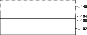
- 2 shows a cross section of the semiconductor device 100 in the manufacturing process.
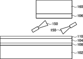
- 2 shows a cross section of the semiconductor device 100 in the manufacturing process.
- 2 shows a cross section of the semiconductor device 100 in the manufacturing process.
- 2 shows a cross section of the semiconductor device 100 in the manufacturing process.
- 2 shows a cross section of the semiconductor device 100 in the manufacturing process.
- 2 shows a cross section of the semiconductor device 100 in the manufacturing process.
- 2 shows a cross section of the semiconductor device 100 in the manufacturing process.
- the cross section in the manufacture process of another semiconductor device is shown.
- the cross section in the manufacture process of another semiconductor device is shown.
- the cross section in the manufacture process of another semiconductor device is shown.
- the cross section in the manufacture process of another semiconductor device is shown.
- a cross section of a semiconductor device 200 is shown.
- FIG. 1 shows a cross section of the semiconductor device 100.
- the semiconductor device 100 includes a base substrate 102, a first semiconductor crystal layer 104, and a second semiconductor crystal layer 106.
- the semiconductor device 100 of this example includes a first separation layer 108 between the base substrate 102 and the first semiconductor crystal layer 104, and a second separation between the first semiconductor crystal layer 104 and the second semiconductor crystal layer 106.
- a separation layer 110 is included.
- the semiconductor device 100 of this example includes an insulating layer 112 on the second semiconductor crystal layer 106. Note that, from the embodiment shown in FIG. 1, the invention of a semiconductor substrate comprising the base substrate 102, the first semiconductor crystal layer 104, and the second semiconductor crystal layer 106, the base substrate 102, and the first separation.
- At least two inventions can be grasped, including the semiconductor substrate invention having the layer 108, the first semiconductor crystal layer 104, the second separation layer 110, and the second semiconductor crystal layer 106 as constituent elements.
- a first MISFET 120 is formed on the first semiconductor crystal layer 104
- a second MISFET 130 is formed on the second semiconductor crystal layer 106.
- Examples of the base substrate 102 include a substrate whose surface is a silicon crystal.
- Examples of the substrate whose surface is a silicon crystal include a silicon substrate and an SOI (Silicon-on-Insulator) substrate, and a silicon substrate is preferable.
- SOI Silicon-on-Insulator
- the base substrate 102 is not limited to a substrate whose surface is a silicon crystal, and may be an insulator substrate such as glass, ceramics, and plastic, a conductor substrate such as metal, or a semiconductor substrate such as silicon carbide.
- the first semiconductor crystal layer 104 is located above the base substrate 102.
- the first semiconductor crystal layer 104 is made of a group IV semiconductor crystal or a group III-V compound semiconductor crystal.
- the thickness of the first semiconductor crystal layer 104 is preferably 20 nm or less. By setting the thickness of the first semiconductor crystal layer 104 to 20 nm or less, the first MISFET 120 having an extremely thin film body can be configured. By making the body of the first MISFET 120 an extremely thin film, the short channel effect can be suppressed and the leakage current of the first MISFET 120 can be reduced.
- the second semiconductor crystal layer 106 is located above a part of the surface of the first semiconductor crystal layer 104. That is, the second semiconductor crystal layer 106 is located above a part of the region of the first semiconductor crystal layer 104, and the region of the first semiconductor crystal layer 104 where the second semiconductor crystal layer 106 is not located above. A part of these functions as a channel of the first MISFET 120.
- the second semiconductor crystal layer 106 is made of a group III-V compound semiconductor crystal or a group IV semiconductor crystal.
- the thickness of the second semiconductor crystal layer 106 is preferably 20 nm or less. By setting the thickness of the second semiconductor crystal layer 106 to 20 nm or less, the second MISFET 130 having an extremely thin film body can be configured. By making the body of the second MISFET 130 an extremely thin film, the short channel effect can be suppressed and the leakage current of the second MISFET 130 can be reduced.
- the group III-V compound semiconductor crystal has a high electron mobility and the group IV semiconductor crystal, particularly Ge, has a high hole mobility, it is preferable to form an N channel MISFET in the group III-V compound semiconductor crystal layer. It is preferable to form a P-channel MISFET in the group IV semiconductor crystal layer. That is, when the first semiconductor crystal layer 104 is made of a group IV semiconductor crystal and the second semiconductor crystal layer 106 is made of a group III-V compound semiconductor crystal, the first MISFET 120 is a P-channel type MISFET and the second MISFET 130 is an N-channel type. A MISFET is preferable.
- the first MISFET 120 is an N-channel MISFET and the second MISFET 130 is a P-channel.
- a type MISFET is preferable.
- Examples of the group IV semiconductor crystal include a Ge crystal and a Si x Ge 1-x (0 ⁇ x ⁇ 1) crystal. When the group IV semiconductor crystal is a Si x Ge 1-x crystal, x is preferably 0.10 or less.
- Examples of the III-V compound semiconductor crystal include In x Ga 1-x As (0 ⁇ x ⁇ 1) crystal, InAs crystal, GaAs crystal, and InP crystal. Examples of the III-V compound semiconductor crystal include a mixed crystal of a III-V compound semiconductor that lattice matches or pseudo-lattice matches with GaAs or InP.
- examples of the III-V compound semiconductor crystal include a stacked body of the above mixed crystal and an In x Ga 1-x As (0 ⁇ x ⁇ 1) crystal, InAs crystal, GaAs crystal, or InP crystal.
- In x Ga 1-x As (0 ⁇ x ⁇ 1) crystal and InAs crystal are preferable, and InAs crystal is more preferable.
- the first separation layer 108 is located between the base substrate 102 and the first semiconductor crystal layer 104.
- the first separation layer 108 electrically separates the base substrate 102 and the first semiconductor crystal layer 104.
- the first separation layer 108 may be made of an amorphous insulator.
- the first separation layer 108 is made of an amorphous insulator.
- the first separation layer 108 may be made of a semiconductor crystal having a forbidden band width larger than the forbidden band width of the semiconductor crystal constituting the first semiconductor crystal layer 104. Such a semiconductor crystal can be formed by an epitaxial growth method.
- the semiconductor crystal constituting the first separation layer 108 include an AlGaAs crystal, an AlInGaP crystal, an AlGaInAs crystal, and an InP crystal.
- the semiconductor crystal constituting the first separation layer 108 includes a SiGe crystal, a Si crystal, a SiC crystal, or a C crystal.
- the second separation layer 110 is located between the first semiconductor crystal layer 104 and the second semiconductor crystal layer 106.
- the second separation layer 110 electrically separates the first semiconductor crystal layer 104 and the second semiconductor crystal layer 106.
- the second separation layer 110 may be made of an amorphous insulator.
- the second separation layer 110 becomes an amorphous insulator.
- the second separation layer 110 made of an amorphous insulator Al 2 O 3 , AlN, Ta 2 O 5 , ZrO 2 , HfO 2 , La 2 O 3 , SiO x (for example, SiO 2 ), SiN x (for example, Si) 3 N 4 ) and SiO x N y , or a laminate of at least two layers selected from these layers.
- the second isolation layer 110 may be made of a semiconductor crystal having a forbidden band width larger than the forbidden band width of the semiconductor crystal constituting the second semiconductor crystal layer 106. Such a semiconductor crystal can be formed by an epitaxial growth method.
- the semiconductor crystal layer 106 is an InGaAs crystal layer or a GaAs crystal layer
- examples of the semiconductor crystal constituting the second separation layer 110 include an AlGaAs crystal, an AlInGaP crystal, an AlGaInAs crystal, and an InP crystal.
- examples of the semiconductor crystal constituting the second separation layer 110 include SiGe crystal, Si crystal, SiC crystal, and C crystal.
- the insulating layer 112 functions as a gate insulating layer of the second MISFET 130.
- Al 2 O 3 , AlN, Ta 2 O 5 , ZrO 2 , HfO 2 , La 2 O 3 , SiO x (for example, SiO 2 ), SiN x (for example, Si 3 N 4 ), and SiO x N y a layer composed of at least one of them, or a laminate of at least two layers selected from these.
- the first MISFET 120 has a first gate 122, a first source 124 and a first drain 126.
- the first source 124 and the first drain 126 are formed in the first semiconductor crystal layer 104.
- the first MISFET 120 is formed in the first semiconductor crystal layer 104 in a region where the second semiconductor crystal layer 106 is not located above, and a part 104 a of the first semiconductor crystal layer 104 sandwiched between the first source 124 and the first drain 126 is formed.
- Channel The first gate 122 is formed above the part 104a.
- a part 110 a of the second isolation layer 110 is formed in a region sandwiched between the part 104 a of the first semiconductor crystal layer 104 and the first gate 122 which is a channel region.
- the part 110 a may function as a gate insulating layer of the first MISFET 120.
- the first source 124 and the first drain 126 are made of a compound of an atom constituting the first semiconductor crystal layer 104 and a nickel atom.
- the first source 124 and the first drain 126 are made of a compound of atoms and cobalt atoms constituting the first semiconductor crystal layer 104.
- the first source 124 and the first drain 126 are made of a compound of atoms, nickel atoms, and cobalt atoms constituting the first semiconductor crystal layer 104.
- the nickel compound, cobalt compound, or nickel-cobalt compound constituting the first semiconductor crystal layer 104 is a low resistance compound having low electrical resistance.
- the second MISFET 130 has a second gate 132, a second source 134, and a second drain 136.
- the second source 134 and the second drain 136 are formed in the second semiconductor crystal layer 106.
- the second MISFET 130 uses a part 106 a of the second semiconductor crystal layer 106 sandwiched between the second source 134 and the second drain 136 as a channel.
- the second gate 132 is formed above the part 106a.
- a part 112 a of the insulating layer 112 is formed in a region sandwiched between the part 106 a of the second semiconductor crystal layer 106 and the second gate 132 which is a channel region.
- the part 112 a may function as a gate insulating layer of the second MISFET 130.
- the second source 134 and the second drain 136 are made of a compound of atoms and nickel atoms constituting the second semiconductor crystal layer 106.
- the second source 134 and the second drain 136 are made of a compound of atoms and cobalt atoms constituting the second semiconductor crystal layer 106.
- the second source 134 and the second drain 136 are made of a compound of atoms, nickel atoms, and cobalt atoms constituting the second semiconductor crystal layer 106.
- the nickel compound, cobalt compound or nickel-cobalt compound constituting the second semiconductor crystal layer 106 is a low resistance compound having low electric resistance.
- the source / drain (first source 124 and first drain 126) of the first MISFET 120 and the source / drain (second source 134 and second drain 136) of the second MISFET 130 are common atoms (nickel atom, cobalt). Atom or both atoms). This is a configuration that enables the manufacture of the part using a material film having a common atom, and simplifies the manufacturing process. Further, by using nickel or cobalt as a common atom or both, the source / drain formed in the group III-V compound semiconductor crystal layer, the source / drain formed in the group IV semiconductor crystal layer, The electric resistance of the source region and the drain region can be lowered. As a result, the manufacturing process can be simplified and the performance of the FET can be improved.
- the first source 124 and the first drain 126 may further include acceptor impurity atoms, and the second source 134 and the second drain 136 may further include donor impurity atoms.
- the first MISFET 120 is an N-channel MISFET and the second MISFET 130 is a P-channel MISFET
- the first source 124 and the first drain 126 may further include donor impurity atoms
- the second source 134 and the second drain 136 It may further contain acceptor impurity atoms.
- donor impurity atoms contained in the source and drain of the N channel MISFET include Si, S, Se, and Ge.
- acceptor impurity atoms contained in the source and drain of the P-channel MISFET include B, Al, Ga, and In.
- FIG. 2 to 8 show cross sections in the manufacturing process of the semiconductor device 100.
- the base substrate 102 and the semiconductor crystal layer forming substrate 140 are prepared, and the first semiconductor crystal layer 104 is formed on the semiconductor crystal layer forming substrate 140 by an epitaxial growth method. Thereafter, a first separation layer 108 is formed on the first semiconductor crystal layer 104.
- the first separation layer 108 is formed by a thin film formation method such as an ALD (Atomic Layer Deposition) method, a thermal oxidation method, a vapor deposition method, a CVD (Chemical Layer Vapor Deposition) method, or a sputtering method.
- the semiconductor crystal layer formation substrate 140 When the first semiconductor crystal layer 104 is made of a III-V group compound semiconductor crystal, an InP substrate or a GaAs substrate can be selected as the semiconductor crystal layer formation substrate 140. When the first semiconductor crystal layer 104 is made of a group IV semiconductor crystal, a Ge substrate, Si substrate, SiC substrate, or GaAs substrate can be selected as the semiconductor crystal layer formation substrate 140.
- a MOCVD Metal Organic Chemical Vapor Deposition
- TMIn trimethylindium
- TMGa trimethylgallium
- AsH 3 arsine
- P source is used.
- PH 3 phosphine
- Hydrogen can be used as the carrier gas.
- the reaction temperature can be appropriately selected in the range of 300 ° C. to 900 ° C., preferably in the range of 450 to 750 ° C.
- GeH 4 germane
- SiH 4 silane
- Si 2 H 6 diisilane
- a compound in which some of these hydrogen atoms are substituted with chlorine atoms or hydrocarbon groups can also be used.
- Hydrogen can be used as the carrier gas.
- the reaction temperature can be appropriately selected in the range of 300 ° C. to 900 ° C., preferably in the range of 450 to 750 ° C.
- the thickness of the epitaxial growth layer can be controlled by appropriately selecting the source gas supply amount and the reaction time.
- the surface of the first separation layer 108 and the surface of the base substrate 102 are activated with an argon beam 150. Thereafter, as shown in FIG. 3, the surface of the first separation layer 108 activated by the argon beam 150 and the surface of the base substrate 102 are bonded and bonded together. Bonding can be performed at room temperature. The activation does not need to be performed by the argon beam 150, but may be a beam of other rare gas or the like. Thereafter, the semiconductor crystal layer forming substrate 140 is etched and removed. As a result, the first separation layer 108 and the first semiconductor crystal layer 104 are formed on the base substrate 102. Note that a sulfur termination treatment for terminating the surface of the first semiconductor crystal layer 104 with sulfur atoms may be performed between the formation of the first semiconductor crystal layer 104 and the formation of the first separation layer 108.
- the first separation layer 108 is formed only on the first semiconductor crystal layer 104 and the surface of the first separation layer 108 and the surface of the base substrate 102 are bonded to each other.
- the first separation layer 108 is also formed on the base substrate 102, and the surface of the first separation layer 108 on the first semiconductor crystal layer 104 and the surface of the first separation layer 108 on the base substrate 102 are bonded together. May be.
- the surface of the first separation layer 108 to be bonded is subjected to a hydrophilic treatment. When the hydrophilic treatment is performed, it is preferable that the first separation layers 108 are heated and bonded together.
- the first separation layer 108 may be formed only on the base substrate 102, and the surface of the first semiconductor crystal layer 104 and the surface of the first separation layer 108 on the base substrate 102 may be bonded to each other.
- the first separation layer 108 and the first semiconductor crystal layer 104 are bonded to the semiconductor crystal layer formation substrate.
- the first separation layer 108 and the first semiconductor crystal layer 104 are separated from the base substrate 102. You may stick together.
- the first separation layer 108 and the first semiconductor crystal layer 104 are separated from the semiconductor crystal layer formation substrate 140 and before being bonded to the base substrate 102, the first separation layer 108 and the first separation layer 108 are formed on an appropriate transfer substrate. It is preferable to hold one semiconductor crystal layer 104.
- a semiconductor crystal layer forming substrate 160 is prepared, and the second semiconductor crystal layer 106 is formed on the semiconductor crystal layer forming substrate 160 by an epitaxial growth method.
- a second separation layer 110 is formed on the first semiconductor crystal layer 104 on the base substrate 102.
- the second separation layer 110 is formed by a thin film forming method such as an ALD method, a thermal oxidation method, a vapor deposition method, a CVD method, or a sputtering method.
- a sulfur termination treatment for terminating the surface of the first semiconductor crystal layer 104 with sulfur atoms may be performed before the formation of the second separation layer 110.
- the semiconductor crystal layer 106 is made of a III-V group compound semiconductor crystal
- an InP substrate or a GaAs substrate can be selected as the semiconductor crystal layer forming substrate 160.
- the second semiconductor crystal layer 106 is made of a group IV semiconductor crystal
- a Ge substrate, Si substrate, SiC substrate, or GaAs substrate can be selected as the semiconductor crystal layer forming substrate 160.
- the MOCVD method can be used for epitaxial growth of the second semiconductor crystal layer 106.
- Gas used in the MOCVD method, reaction temperature conditions, and the like are the same as those for the first semiconductor crystal layer 104.
- the surface of the second semiconductor crystal layer 106 and the surface of the second separation layer 110 are activated with an argon beam 150. Thereafter, as shown in FIG. 5, the surface of the second semiconductor crystal layer 106 is bonded to and bonded to a part of the surface of the second separation layer 110. Bonding can be performed at room temperature. The activation does not need to be performed by the argon beam 150 but may be a beam of other rare gas or the like. Thereafter, the semiconductor crystal layer forming substrate 160 is removed by etching with an HCl solution or the like.
- the second separation layer 110 is formed on the first semiconductor crystal layer 104 on the base substrate 102, and the second semiconductor crystal layer 106 is formed on a part of the surface of the second separation layer 110.
- a sulfur termination treatment may be performed in which the surface of the second semiconductor crystal layer 106 is terminated with sulfur atoms.
- the second separation layer 110 is formed only on the first semiconductor crystal layer 104 and the surface of the second separation layer 110 and the surface of the second semiconductor crystal layer 106 are bonded to each other has been described.
- the second separation layer 110 is also formed on the second semiconductor crystal layer 106, and the surface of the second separation layer 110 on the first semiconductor crystal layer 104 and the second separation layer 110 on the second semiconductor crystal layer 106 are formed. You may stick together the surface.
- the second separation layer 110 is formed only on the second semiconductor crystal layer 106, and the surface of the first semiconductor crystal layer 104 and the surface of the second separation layer 110 on the second semiconductor crystal layer 106 are bonded together. Also good.
- the second semiconductor crystal layer 106 is separated from the semiconductor crystal layer formation substrate 160 after the second semiconductor crystal layer 106 is bonded to the second separation layer 110 on the base substrate 102 has been described.
- the second semiconductor crystal layer 106 may be bonded to the second separation layer 110.
- the second semiconductor crystal layer 106 may be held on an appropriate transfer substrate until the second semiconductor crystal layer 106 is bonded to the second separation layer 110. preferable.
- an insulating layer 112 is formed on the second semiconductor crystal layer 106.
- the insulating layer 112 is formed by a thin film forming method such as an ALD method, a thermal oxidation method, a vapor deposition method, a CVD method, or a sputtering method. Further, a thin film of a metal such as tantalum such as tantalum is formed by vapor deposition, CVD, or sputtering, and the thin film is patterned using photolithography, so that the first semiconductor crystal layer in which the second semiconductor crystal layer 106 is not formed A first gate 122 is formed above 104, and a second gate 132 is formed above the second semiconductor crystal layer 106.
- openings reaching the first semiconductor crystal layer 104 are formed in the second isolation layer 110 on both sides of the first gate 122, and the second semiconductor crystal is formed on the insulating layer 112 on both sides of the second gate 132.
- An opening reaching layer 106 is formed.
- the both sides of each gate indicate both sides of each gate in the horizontal direction.
- the openings on both sides of the first gate 122 and the openings on both sides of the second gate 132 correspond to regions where the first source 124, the first drain 126, the second source 134, and the second drain 136 are formed.
- a metal film 170 made of nickel is formed so as to be in contact with each of the first semiconductor crystal layer 104 and the second semiconductor crystal layer 106 exposed at the bottom of these openings.
- the metal film 170 may be a cobalt film or a nickel-cobalt alloy film.
- the metal film 170 is heated.
- the first semiconductor crystal layer 104 and the metal film 170 react to form a low-resistance compound of atoms constituting the first semiconductor crystal layer 104 and atoms constituting the metal film 170, and the first source 124. And the first drain 126.
- the second semiconductor crystal layer 106 and the metal film 170 react to form a low-resistance compound of atoms constituting the second semiconductor crystal layer 106 and atoms constituting the metal film 170, and the second source 134 and A second drain 136 is formed.
- the metal film 170 is a nickel film
- a low resistance compound of atoms and nickel atoms constituting the first semiconductor crystal layer 104 is generated as the first source 124 and the first drain 126, and the second source 134 and the second source 126 are formed.
- the drain 136 a low-resistance compound of atoms and nickel atoms constituting the second semiconductor crystal layer 106 is generated.
- the metal film 170 is a cobalt film
- low resistance compounds of atoms and cobalt atoms forming the first semiconductor crystal layer 104 are generated as the first source 124 and the first drain 126, and the second source 134 and As the second drain 136, a low resistance compound of atoms and cobalt atoms constituting the second semiconductor crystal layer 106 is generated.
- the metal film 170 is a nickel-cobalt alloy film
- low resistance compounds of atoms, nickel atoms, and cobalt atoms forming the first semiconductor crystal layer 104 are generated as the first source 124 and the first drain 126
- the first As the two sources 134 and the second drain 136 a low resistance compound of atoms, nickel atoms, and cobalt atoms constituting the second semiconductor crystal layer 106 is generated.
- the unreacted metal film 170 is removed, and the semiconductor device 100 of FIG. 1 can be manufactured.
- the heating method of the metal film 170 is preferably an RTA (rapid thermal annealing) method.
- RTA rapid thermal annealing
- a heating temperature of 250 ° C. to 450 ° C. can be used.
- the first source 124, the first drain 126, the second source 134, and the second drain 136 can be formed by self-alignment.
- the first source 124, the first drain 126, the second source 134, and the second drain 136 are simultaneously formed in the same process, so that the manufacturing process can be simplified. . As a result, manufacturing costs are reduced and miniaturization is facilitated. Further, the first source 124, the first drain 126, the second source 134, and the second drain 136 are atoms constituting the first semiconductor crystal layer 104 or the second semiconductor crystal layer 106, that is, a group IV atom or a group III-V. It is a low resistance compound of atoms and nickel, cobalt or nickel-cobalt alloy.
- the contact potential barrier between these low-resistance compounds and the first semiconductor crystal layer 104 and the second semiconductor crystal layer 106 constituting the channel of the semiconductor device 100 is as small as 0.1 eV or less. Further, the contact between each of the first source 124, the first drain 126, the second source 134, and the second drain 136 and the electrode metal becomes an ohmic contact, and the on-currents of the first MISFET 120 and the second MISFET 130 can be increased.
- the resistances of the first source 124, the first drain 126, the second source 134, and the second drain 136 are reduced, it is not necessary to reduce the channel resistance of the first MISFET 120 and the second MISFET 130, and the concentration of doping impurity atoms is reduced. Less. As a result, carrier mobility in the channel layer can be increased.
- the first separation layer of the base substrate 102 is used.
- a voltage can be applied to a region in contact with 108, and the voltage can act as a back gate voltage to the first MISFET 120.
- a voltage can be applied to a region of the first semiconductor crystal layer 104 that is in contact with the second isolation layer 110, and the voltage can act as a back gate voltage to the second MISFET 130.
- the action of these back gate voltages can increase the on-current of the first MISFET 120 and the second MISFET 130 and reduce the off-current.
- the semiconductor device 100 described above may include a plurality of second semiconductor crystal layers 106, and each of the plurality of second semiconductor crystal layers 106 may be regularly arranged in a plane parallel to the upper surface of the base substrate 102.
- the semiconductor device 100 may include a plurality of first semiconductor crystal layers 104, and each of the plurality of first semiconductor crystal layers 104 may be regularly arranged in a plane parallel to the upper surface of the base substrate 102.
- Good. Regular means that the same arrangement pattern is repeated, for example.
- each first semiconductor crystal layer 104 may have a single semiconductor crystal layer 106 or a plurality of second semiconductor crystal layers 106, and each second semiconductor crystal layer 106 is parallel to the upper surface of the first semiconductor crystal layer 104. May be regularly arranged in a plane.
- the productivity of the semiconductor substrate used for the semiconductor device 100 can be increased.
- the regular arrangement of the second semiconductor crystal layer 106 or the first semiconductor crystal layer 104 is such that the second semiconductor crystal layer 106 or the first semiconductor crystal layer is grown after the second semiconductor crystal layer 106 or the first semiconductor crystal layer 104 is epitaxially grown.
- the first semiconductor crystal layer 104 and the first isolation layer 108 are formed on the semiconductor crystal layer formation substrate 140, and the first isolation layer 108 and the base substrate 102 are bonded together, and then the semiconductor crystal layer formation is performed. It has been described that the first semiconductor crystal layer 104 and the first separation layer 108 are formed on the base substrate 102 by removing the substrate 140. However, when the first semiconductor crystal layer 104 is made of SiGe and the second semiconductor crystal layer 106 is made of a group III-V compound semiconductor crystal, the first semiconductor crystal layer 104 and the first separation layer 108 are formed by an oxidation concentration method.
- the first separation layer 108 made of an insulator is formed on the base substrate 102, and the first semiconductor crystal layer 104 starts on the first separation layer 108.
- a SiGe layer as a material is formed.
- the SiGe layer is heated in an oxidizing atmosphere to oxidize the surface. By oxidizing the SiGe layer, the concentration of Ge atoms in the SiGe layer can be increased, and the first semiconductor crystal layer 104 having a high Ge concentration can be obtained.
- the first semiconductor crystal layer 104 and the first separation layer 108 are smart cut. It can be formed by the method. That is, a first separation layer 108 made of an insulator is formed on the surface of a semiconductor layer material substrate made of a group IV semiconductor crystal, and cations are implanted through the first separation layer 108 to a predetermined separation depth of the semiconductor layer material substrate. To do. The semiconductor layer material substrate and the base substrate 102 are attached to each other so that the surface of the first separation layer 108 and the surface of the base substrate 102 are bonded, and the semiconductor layer material substrate and the base substrate 102 are heated.
- the cations implanted at the planned separation depth react with the group IV atoms constituting the semiconductor layer material substrate, and the group IV semiconductor crystal located at the planned separation depth is denatured. If the semiconductor layer material substrate and the base substrate 102 are separated in this state, the group IV semiconductor crystal located on the base substrate 102 side from the modified group of the group IV semiconductor crystal is separated from the semiconductor layer material substrate. If the semiconductor layer material attached to the base substrate 102 side is appropriately polished, the polished semiconductor crystal layer can be used as the first semiconductor crystal layer 104.
- the first isolation layer 108 when the first separation layer 108 is a semiconductor crystal having a forbidden band width larger than the forbidden band width of the semiconductor crystal constituting the first semiconductor crystal layer 104,
- the first isolation layer 108 can be formed by an epitaxial growth method, and the first semiconductor crystal layer 104 can be formed on the first isolation layer 108 by an epitaxial growth method. Since the first separation layer 108 and the first semiconductor crystal layer 104 can be continuously formed by the epitaxial growth method, the manufacturing process is simplified.
- the second separation layer 110 is a semiconductor crystal having a forbidden band width larger than that of the semiconductor crystal constituting the second semiconductor crystal layer 106
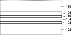
- the second semiconductor crystal layer 106, the second The two separation layers 110 and the first semiconductor crystal layer 104 can be continuously formed by an epitaxial growth method. That is, as shown in FIG. 9, the second semiconductor crystal layer 106 is formed on the semiconductor crystal layer forming substrate 180 by the epitaxial growth method, and the second separation layer 110 is formed on the second semiconductor crystal layer 106 by the epitaxial growth method. Then, the first semiconductor crystal layer 104 is formed on the second separation layer 110 by an epitaxial growth method. These epitaxial growths can be performed continuously.
- a first separation layer 108 is formed on the first semiconductor crystal layer 104, and the surface of the first separation layer 108 and the surface of the base substrate 102 are activated with an argon beam 150.
- the surface of the first separation layer 108 and the surface of the base substrate 102 are bonded together, and the semiconductor crystal layer forming substrate 180 is etched and removed with an HCl solution or the like.
- a part of the second semiconductor crystal layer 106 is etched using a mask 185, whereby a semiconductor substrate similar to that in FIG. 5 can be obtained.
- the second semiconductor crystal layer 106, the second separation layer 110, and the first semiconductor crystal layer 104 can be continuously formed by an epitaxial growth method, so that the manufacturing process is simplified.
- the first step is performed on either or both of the base substrate 102 and the first semiconductor crystal layer 104.
- One separation layer 108 may be formed.
- the first separation layer 108, the first semiconductor crystal layer 104, the second separation layer 110, and the second semiconductor crystal layer 106 may be transferred to an appropriate transfer substrate and then bonded to the base substrate 102.
- the second isolation layer 110 is an epitaxially grown crystal
- the first isolation crystal layer 104, the second isolation layer 110, and the second semiconductor crystal layer 106 are bonded to the base substrate 102, and then the second isolation layer 110 is oxidized. Then, it may be converted into an amorphous insulator layer.
- the second separation layer 110 is AlAs or AlInP
- the second separation layer 110 can be made of an insulating oxide by a selective oxidation technique.
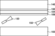
- the substrate can also be removed. That is, before forming the first semiconductor crystal layer 104 on the semiconductor crystal layer formation substrate 140, the crystalline sacrificial layer 190 is formed on the surface of the semiconductor crystal layer formation substrate 140 by an epitaxial growth method. Thereafter, the first semiconductor crystal layer 104 and the first separation layer 108 are formed on the surface of the crystalline sacrificial layer 190 by an epitaxial growth method, and the surface of the first separation layer 108 and the surface of the base substrate 102 are activated by the argon beam 150. .
- the semiconductor crystal layer forming substrate 140 can be reused, and the manufacturing cost can be reduced.
- FIG. 14 shows a cross section of the semiconductor device 200.
- the semiconductor device 200 does not have the first separation layer 108 in the semiconductor device 100, and the first semiconductor crystal layer 104 is disposed in contact with the base substrate 102.
- the first separation layer 108 since it has the same structure as the semiconductor device 100 except that the first separation layer 108 is not provided, description of common members and the like is omitted.
- the base substrate 102 and the first semiconductor crystal layer 104 are in contact with each other at the bonding surface 103, and contain impurity atoms having p-type or n-type conductivity in the vicinity of the bonding surface 103 of the base substrate 102.
- impurity atoms having a conductivity type different from the conductivity type indicated by the impurity atoms contained in the base substrate 102 are contained. That is, the semiconductor device 200 has a pn junction in the vicinity of the bonding surface 103.
- the base substrate 102 and the first semiconductor crystal layer 104 can be electrically separated by a pn junction formed in the vicinity of the bonding surface 103.
- the first MISFET 120 formed in the semiconductor crystal layer 104 can be electrically isolated from the base substrate 102.
- Such separation by the pn junction can also be applied between the first semiconductor crystal layer 104 and the second semiconductor crystal layer 106. That is, in the structure in which the second semiconductor layer 104 is not in contact with the first semiconductor crystal layer 104 and the second semiconductor crystal layer 106 are in contact with each other at the junction surface, the p-type or An impurity atom having an n-type conductivity type is contained, and a conductivity type different from the conductivity type indicated by the impurity atom contained in the first semiconductor crystal layer 104 is present in the vicinity of the junction surface of the second semiconductor crystal layer 106. Contains impurity atoms.
- first semiconductor crystal layer 104 and the second semiconductor crystal layer 106 can be electrically separated, and the first MISFET 120 formed in the first semiconductor crystal layer 104 and the second MISFET 130 formed in the second semiconductor crystal layer 106 are electrically connected. Can be separated.
- the steps after the step of forming the first semiconductor crystal layer 104 on the base substrate 102 by the epitaxial growth method and forming the second isolation layer 110 on the first semiconductor crystal layer 104 are the same as those in the semiconductor device 200. It can be manufactured by performing the same process as in the case of the device 100.
- the base substrate 102 is formed in a step in which impurity atoms having p-type or n-type conductivity are contained in the vicinity of the surface of the base substrate 102 and the first semiconductor crystal layer 104 is formed by the epitaxial growth method.
- the first semiconductor crystal layer 104 can be doped with an impurity atom having a conductivity type different from that of the impurity atom contained in the first semiconductor crystal layer 104.
- the pn junction as the isolation structure is not essential when the need for element isolation is low. That is, the semiconductor device 200 does not contain an impurity atom having p-type or n-type conductivity in the vicinity of the bonding surface 103 of the base substrate 102, and is p-type or in the vicinity of the bonding surface 103 of the first semiconductor crystal layer 104. A structure not containing an impurity atom exhibiting n-type conductivity may be used.
- the epitaxial growth method is a method in which the first semiconductor crystal layer 104 is uniformly grown on the entire surface of the base substrate 102, or the surface of the base substrate 102 is divided finely by a growth inhibition layer such as SiO 2 and selectively. Any epitaxial growth method may be used.
- 100 semiconductor device 102 base substrate, 103 bonding surface, 104 first semiconductor crystal layer, 104a part of first semiconductor crystal layer, 106 second semiconductor crystal layer, 106a part of second semiconductor crystal layer, 108 first separation 110, second isolation layer, 110a part of second isolation layer, 112 insulating layer, part of 112a insulating layer, 120 first MISFET, 122 first gate, 124 first source, 126 first drain, 130 second MISFET 132, second gate, 134 second source, 136 second drain, 140 semiconductor crystal layer forming substrate, 150 argon beam, 160 semiconductor crystal layer forming substrate, 170 metal film, 180 semiconductor crystal layer forming substrate, 185 mask, 190 crystal Sacrificial layer, 200 semiconductor devices
Landscapes
- Metal-Oxide And Bipolar Metal-Oxide Semiconductor Integrated Circuits (AREA)
- Thin Film Transistor (AREA)
- Recrystallisation Techniques (AREA)
- Insulated Gate Type Field-Effect Transistor (AREA)
Abstract
Description
非特許文献1 S. Takagi, et al., SSE, vol. 51, pp. 526-536, 2007.
Claims (26)
- ベース基板と、
前記ベース基板の上方に位置する第1半導体結晶層と、
前記第1半導体結晶層における一部の領域の上方に位置する第2半導体結晶層と、
前記第2半導体結晶層が上方に位置しない前記第1半導体結晶層の領域の一部をチャネルとし、第1ソースおよび第1ドレインを有する第1MISFETと、
前記第2半導体結晶層の一部をチャネルとし、第2ソースおよび第2ドレインを有する第2MISFETと、を有し、
前記第1MISFETが、第1チャネル型のMISFETであり、前記第2MISFETが、前記第1チャネル型とは相違する第2チャネル型のMISFETであり、
前記第1ソースおよび前記第1ドレインが、前記第1半導体結晶層を構成する原子とニッケル原子との化合物、前記第1半導体結晶層を構成する原子とコバルト原子との化合物、または、前記第1半導体結晶層を構成する原子とニッケル原子とコバルト原子との化合物からなり、
前記第2ソースおよび前記第2ドレインが、前記第2半導体結晶層を構成する原子とニッケル原子との化合物、前記第2半導体結晶層を構成する原子とコバルト原子との化合物、または、前記第2半導体結晶層を構成する原子とニッケル原子とコバルト原子との化合物からなる
半導体デバイス。 - 前記ベース基板と前記第1半導体結晶層との間に位置し、前記ベース基板と前記第1半導体結晶層とを電気的に分離する第1分離層と、
前記第1半導体結晶層と前記第2半導体結晶層との間に位置し、前記第1半導体結晶層と前記第2半導体結晶層とを電気的に分離する第2分離層と、をさらに有する
請求項1に記載の半導体デバイス。 - 前記第1半導体結晶層と前記第2半導体結晶層との間に位置し、前記第1半導体結晶層と前記第2半導体結晶層とを電気的に分離する第2分離層をさらに有し、
前記ベース基板と前記第1半導体結晶層とが接合面で接し、
前記接合面の近傍における前記ベース基板の領域に、p型またはn型の伝導型を示す不純物原子を含有し、
前記接合面の近傍における前記第1半導体結晶層の領域に、前記ベース基板に含有された不純物原子が示す伝導型とは異なる伝導型を示す不純物原子を含有する
請求項1に記載の半導体デバイス。 - 前記ベース基板と前記第1分離層とが接し、
前記ベース基板の前記第1分離層と接する領域が導電性であり、
前記ベース基板の前記第1分離層と接する領域に印加した電圧が、前記第1MISFETへのバックゲート電圧として作用する
請求項2に記載の半導体デバイス。 - 前記第1半導体結晶層と前記第2分離層とが接し、
前記第1半導体結晶層の前記第2分離層と接する領域が導電性であり、
前記第1半導体結晶層の前記第2分離層と接する領域に印加した電圧が、前記第2MISFETへのバックゲート電圧として作用する
請求項2に記載の半導体デバイス。 - 前記第1半導体結晶層がIV族半導体結晶からなり、前記第1MISFETがPチャネル型MISFETであり、
前記第2半導体結晶層がIII-V族化合物半導体結晶からなり、前記第2MISFETがNチャネル型MISFETである
請求項1に記載の半導体デバイス。 - 前記第1半導体結晶層がIII-V族化合物半導体結晶からなり、前記第1MISFETがNチャネル型MISFETであり、
前記第2半導体結晶層がIV族半導体結晶からなり、前記第2MISFETがPチャネル型MISFETである
請求項1に記載の半導体デバイス。 - 請求項1に記載の半導体デバイスに用いる半導体基板であって、
前記ベース基板と、前記第1半導体結晶層と、前記第2半導体結晶層と、を有し、
前記第1半導体結晶層が、前記ベース基板の上方に位置し、
前記第2半導体結晶層が、前記第1半導体結晶層の一部または全部の上方に位置する
半導体基板。 - 前記ベース基板と前記第1半導体結晶層との間に位置し、前記ベース基板と前記第1半導体結晶層とを電気的に分離する第1分離層と、
前記第1半導体結晶層と前記第2半導体結晶層との間に位置し、前記第1半導体結晶層と前記第2半導体結晶層とを電気的に分離する第2分離層と、をさらに有する
請求項8に記載の半導体基板。 - 前記第1分離層が、非晶質絶縁体からなる
請求項9に記載の半導体基板。 - 前記第1分離層が、前記第1半導体結晶層を構成する半導体結晶の禁制帯幅より大きな禁制帯幅を有する半導体結晶からなる
請求項9に記載の半導体基板。 - 前記第1半導体結晶層と前記第2半導体結晶層との間に位置し、前記第1半導体結晶層と前記第2半導体結晶層とを電気的に分離する第2分離層をさらに有し、
前記ベース基板と前記第1半導体結晶層とが接合面で接し、
前記接合面の近傍における前記ベース基板の領域に、p型またはn型の伝導型を示す不純物原子を含有し、
前記接合面の近傍における前記第1半導体結晶層の領域に、前記ベース基板に含有された不純物原子が示す伝導型とは異なる伝導型を示す不純物原子を含有する
請求項8に記載の半導体基板。 - 前記第2分離層が、非晶質絶縁体からなる
請求項9に記載の半導体基板。 - 前記第2分離層が、前記第2半導体結晶層を構成する半導体結晶の禁制帯幅より大きな禁制帯幅を有する半導体結晶からなる
請求項9に記載の半導体基板。 - 前記第2半導体結晶層を複数有し、
複数の前記第2半導体結晶層のそれぞれが、前記ベース基板の上面と平行な面内で規則的に配列されている
請求項8に記載の半導体基板。 - 請求項8に記載の半導体基板を製造する方法であって、
前記ベース基板の上方に前記第1半導体結晶層を形成する第1半導体結晶層形成ステップと、
前記第1半導体結晶層における一部の領域の上方に前記第2半導体結晶層を形成する第2半導体結晶層形成ステップと、を有し、
前記第2半導体結晶層形成ステップが、
半導体結晶層形成基板上に前記第2半導体結晶層をエピタキシャル成長法により形成するエピタキシャル成長ステップと、
前記第1半導体結晶層の上、前記第2半導体結晶層の上、または、前記第1半導体結晶層および前記第2半導体結晶層の両方の上に、前記第1半導体結晶層と前記第2半導体結晶層とを電気的に分離する第2分離層を形成するステップと、
前記第1半導体結晶層上の前記第2分離層と前記第2半導体結晶層とが接合するように、前記第2半導体結晶層上の前記第2分離層と前記第1半導体結晶層とが接合するように、または、前記第1半導体結晶層上の前記第2分離層と前記第2半導体結晶層上の前記第2分離層とが接合するように、前記第1半導体結晶層を有する前記ベース基板と、前記半導体結晶層形成基板とを貼り合わせる貼り合わせステップと、
を有する半導体基板の製造方法。 - 前記第1半導体結晶層形成ステップが、
半導体結晶層形成基板上に前記第1半導体結晶層をエピタキシャル成長法により形成するエピタキシャル成長ステップと、
前記ベース基板の上、前記第1半導体結晶層の上、または、前記ベース基板および前記第1半導体結晶層の両方の上に、前記ベース基板と前記第1半導体結晶層とを電気的に分離する第1分離層を形成するステップと、
前記ベース基板上の前記第1分離層と前記第1半導体結晶層とが接合するように、前記第1半導体結晶層上の前記第1分離層と前記ベース基板とが接合するように、または、前記ベース基板上の前記第1分離層と前記第1半導体結晶層上の前記第1分離層とが接合するように、前記ベース基板と、前記半導体結晶層形成基板とを貼り合わせる貼り合わせステップと、
を有する請求項16に記載の半導体基板の製造方法。 - 前記第1半導体結晶層がSiGeからなり、前記第2半導体結晶層がIII-V族化合物半導体結晶からなり、
前記第1半導体結晶層形成ステップの前に、絶縁体からなる第1分離層を前記ベース基板の上に形成するステップを有し、
前記第1半導体結晶層形成ステップが、
前記第1分離層の上に、前記第1半導体結晶層の出発材料となるSiGe層を形成するステップと、
前記SiGe層を酸化雰囲気中で加熱し、表面を酸化することで前記SiGe層中のGe原子の濃度を高めるステップと、
を有する請求項16に記載の半導体基板の製造方法。 - 前記第1半導体結晶層がIV族半導体結晶からなり、前記第2半導体結晶層がIII-V族化合物半導体結晶からなり、
IV族半導体結晶からなる半導体層材料基板の表面に、絶縁体からなる第1分離層を形成するステップと、
前記第1分離層を通して、陽イオンを前記半導体層材料基板の分離予定深さに注入するステップと、
前記第1分離層の表面と前記ベース基板の表面とが接合されるように、前記半導体層材料基板と前記ベース基板とを貼り合わせるステップと、
前記半導体層材料基板および前記ベース基板を加熱し、前記分離予定深さに注入した前記陽イオンと、前記半導体層材料基板を構成するIV族原子とを反応させることで、前記分離予定深さに位置する前記IV族半導体結晶を変性するステップと、
前記半導体層材料基板と前記ベース基板とを分離することで、前記変性するステップで変性させた前記IV族半導体結晶の変性部位より前記ベース基板側に位置する前記IV族半導体結晶を、前記半導体層材料基板から剥離するステップと、
を有する請求項16に記載の半導体基板の製造方法。 - 前記第1半導体結晶層形成ステップの前に、前記ベース基板の上に前記第1半導体結晶層を構成する半導体結晶の禁制帯幅より大きな禁制帯幅を有する半導体結晶からなる第1分離層をエピタキシャル成長法により形成するステップを有し、
前記第1半導体結晶層形成ステップが、前記第1分離層の上に前記第1半導体結晶層をエピタキシャル成長法により形成するステップである
請求項16に記載の半導体基板の製造方法。 - 前記第1半導体結晶層形成ステップが、前記ベース基板の上に前記第1半導体結晶層をエピタキシャル成長法により形成するステップである
請求項16に記載の半導体基板の製造方法。 - 前記ベース基板の表面近傍に、p型またはn型の伝導型を示す不純物原子を含有し、
前記第1半導体結晶層をエピタキシャル成長法により形成するステップにおいて、前記ベース基板に含有された不純物原子が示す伝導型とは異なる伝導型を示す不純物原子で第1半導体結晶層をドープする
請求項21に記載の半導体基板の製造方法。 - 請求項14に記載の半導体基板を製造する方法であって、
半導体結晶層形成基板の上に前記第2半導体結晶層をエピタキシャル成長法により形成する第2半導体結晶層形成ステップと、
前記第2半導体結晶層の上に、前記第2半導体結晶層を構成する半導体結晶の禁制帯幅より大きな禁制帯幅を有する半導体結晶からなる第2分離層をエピタキシャル成長法により形成する第2分離層形成ステップと、
前記第2分離層の上に前記第1半導体結晶層をエピタキシャル成長法により形成する第1半導体結晶層形成ステップと、
前記ベース基板の上、前記第1半導体結晶層の上、または、前記ベース基板および前記第1半導体結晶層の両方の上に、前記ベース基板と前記第1半導体結晶層とを電気的に分離する第1分離層を形成するステップと、
前記ベース基板上の前記第1分離層と前記第1半導体結晶層とが接合するように、前記第1半導体結晶層上の前記第1分離層と前記ベース基板とが接合するように、または、前記ベース基板上の前記第1分離層と前記第1半導体結晶層上の前記第1分離層とが接合するように、前記ベース基板と、前記半導体結晶層形成基板とを貼り合わせる貼り合わせステップと、
を有する半導体基板の製造方法。 - 前記半導体結晶層形成基板の上に半導体結晶層を形成する前に、前記半導体結晶層形成基板の表面に、結晶性犠牲層をエピタキシャル成長法により形成するステップと、
前記ベース基板と前記半導体結晶層形成基板とを貼り合わせた後に、前記結晶性犠牲層を除去することにより、前記半導体結晶層形成基板上にエピタキシャル成長法により形成された半導体結晶層と前記半導体結晶層形成基板とを分離するステップと、
をさらに有する請求項16に記載の半導体基板の製造方法。 - 前記第2半導体結晶層をエピタキシャル成長させた後に前記第2半導体結晶層を規則的な配列にパターニングするステップ、または前記第2半導体結晶層を予め規則的な配列に選択的にエピタキシャル成長させるステップ、のいずれかのステップを有する
請求項16に記載の半導体基板の製造方法。 - 請求項16に記載の半導体基板の製造方法を用いて、前記第1半導体結晶層および前記第2半導体結晶層を有する半導体基板を製造するステップと、
前記第1半導体結晶層および前記第2半導体結晶層のそれぞれの上にゲート絶縁層を介してゲート電極を形成するステップと、
前記第1半導体結晶層のソース電極形成領域上、前記第1半導体結晶層のドレイン電極形成領域上、前記第2半導体結晶層のソース電極形成領域上、および前記第2半導体結晶層のドレイン電極形成領域上に、ニッケル膜、コバルト膜およびニッケル-コバルト合金膜からなる群から選ばれた金属膜を形成するステップと、
前記金属膜を加熱して、前記第1半導体結晶層に、前記第1半導体結晶層を構成する原子とニッケル原子との化合物、前記第1半導体結晶層を構成する原子とコバルト原子との化合物、または、前記第1半導体結晶層を構成する原子とニッケル原子とコバルト原子との化合物からなる第1ソースおよび第1ドレインを形成し、前記第2半導体結晶層に、前記第2半導体結晶層を構成する原子とニッケル原子との化合物、前記第2半導体結晶層を構成する原子とコバルト原子との化合物、または、前記第2半導体結晶層を構成する原子とニッケル原子とコバルト原子との化合物からなる第2ソースおよび第2ドレインを形成するステップと、
未反応の前記金属膜を除去するステップと、
を有する半導体デバイスの製造方法。
Priority Applications (3)
| Application Number | Priority Date | Filing Date | Title |
|---|---|---|---|
| CN201280024791.0A CN103563068B (zh) | 2011-06-10 | 2012-06-08 | 半导体器件、半导体基板、半导体基板的制造方法及半导体器件的制造方法 |
| KR1020137031864A KR20140033070A (ko) | 2011-06-10 | 2012-06-08 | 반도체 디바이스, 반도체 기판, 반도체 기판의 제조 방법 및 반도체 디바이스의 제조 방법 |
| US14/099,427 US20140091393A1 (en) | 2011-06-10 | 2013-12-06 | Semiconductor device, semiconductor wafer, method for producing semiconductor wafer, and method for producing semiconductor device |
Applications Claiming Priority (2)
| Application Number | Priority Date | Filing Date | Title |
|---|---|---|---|
| JP2011130727 | 2011-06-10 | ||
| JP2011-130727 | 2011-06-10 |
Related Child Applications (1)
| Application Number | Title | Priority Date | Filing Date |
|---|---|---|---|
| US14/099,427 Continuation-In-Part US20140091393A1 (en) | 2011-06-10 | 2013-12-06 | Semiconductor device, semiconductor wafer, method for producing semiconductor wafer, and method for producing semiconductor device |
Publications (1)
| Publication Number | Publication Date |
|---|---|
| WO2012169209A1 true WO2012169209A1 (ja) | 2012-12-13 |
Family
ID=47295792
Family Applications (1)
| Application Number | Title | Priority Date | Filing Date |
|---|---|---|---|
| PCT/JP2012/003769 Ceased WO2012169209A1 (ja) | 2011-06-10 | 2012-06-08 | 半導体デバイス、半導体基板、半導体基板の製造方法および半導体デバイスの製造方法 |
Country Status (6)
| Country | Link |
|---|---|
| US (1) | US20140091393A1 (ja) |
| JP (1) | JP2013016789A (ja) |
| KR (1) | KR20140033070A (ja) |
| CN (1) | CN103563068B (ja) |
| TW (1) | TW201308602A (ja) |
| WO (1) | WO2012169209A1 (ja) |
Families Citing this family (4)
| Publication number | Priority date | Publication date | Assignee | Title |
|---|---|---|---|---|
| WO2015199655A1 (en) | 2014-06-24 | 2015-12-30 | Intel Corporation | Techniques for forming ge/sige-channel and iii-v-channel transistors on the same die |
| KR102034175B1 (ko) * | 2017-05-30 | 2019-10-18 | 한국과학기술연구원 | 수평 배열된 반도체 채널을 가지는 반도체 소자 및 이의 제조 방법 |
| CN107946390A (zh) * | 2017-12-04 | 2018-04-20 | 孙健春 | 一种具有换电网的太阳能电池及制作方法 |
| DE102019125461A1 (de) * | 2018-09-28 | 2020-04-02 | Taiwan Semiconductor Manufacturing Co., Ltd. | Halbleiterstruktur, vorrichtung und verfahren |
Citations (7)
| Publication number | Priority date | Publication date | Assignee | Title |
|---|---|---|---|---|
| JPS59198750A (ja) * | 1983-04-25 | 1984-11-10 | Seiko Epson Corp | 半導体装置 |
| JPS63311768A (ja) * | 1987-06-13 | 1988-12-20 | Fujitsu Ltd | 相補型半導体装置の製造方法 |
| JPH0384960A (ja) * | 1989-08-28 | 1991-04-10 | Nec Corp | 半導体装置 |
| JPH03109740A (ja) * | 1989-09-25 | 1991-05-09 | Hitachi Ltd | 半導体装置 |
| JP2001093987A (ja) * | 1999-07-29 | 2001-04-06 | Stmicroelectronics Inc | Si基板上のGaAs/Geの新規なCMOS回路 |
| JP2006100403A (ja) * | 2004-09-28 | 2006-04-13 | Fujitsu Ltd | 電界効果型トランジスタおよびその製造方法 |
| JP2007103897A (ja) * | 2005-09-09 | 2007-04-19 | Fujitsu Ltd | 電界効果トランジスタおよびその製造方法 |
Family Cites Families (18)
| Publication number | Priority date | Publication date | Assignee | Title |
|---|---|---|---|---|
| JP2608351B2 (ja) * | 1990-08-03 | 1997-05-07 | キヤノン株式会社 | 半導体部材及び半導体部材の製造方法 |
| JPH06275786A (ja) * | 1993-03-23 | 1994-09-30 | Sony Corp | 相補形化合物半導体装置及びその作製方法 |
| JP3376078B2 (ja) * | 1994-03-18 | 2003-02-10 | 富士通株式会社 | 高電子移動度トランジスタ |
| JP3368449B2 (ja) * | 1994-12-28 | 2003-01-20 | 富士通株式会社 | 半導体装置及びその製造方法 |
| JP3512701B2 (ja) * | 2000-03-10 | 2004-03-31 | 株式会社東芝 | 半導体装置及びその製造方法 |
| US20050275018A1 (en) * | 2004-06-10 | 2005-12-15 | Suresh Venkatesan | Semiconductor device with multiple semiconductor layers |
| US7125785B2 (en) * | 2004-06-14 | 2006-10-24 | International Business Machines Corporation | Mixed orientation and mixed material semiconductor-on-insulator wafer |
| JP4617820B2 (ja) * | 2004-10-20 | 2011-01-26 | 信越半導体株式会社 | 半導体ウェーハの製造方法 |
| US7282425B2 (en) * | 2005-01-31 | 2007-10-16 | International Business Machines Corporation | Structure and method of integrating compound and elemental semiconductors for high-performance CMOS |
| US7342287B2 (en) * | 2005-07-19 | 2008-03-11 | International Business Machines Corporation | Power gating schemes in SOI circuits in hybrid SOI-epitaxial CMOS structures |
| US7696574B2 (en) * | 2005-10-26 | 2010-04-13 | International Business Machines Corporation | Semiconductor substrate with multiple crystallographic orientations |
| FR2911721B1 (fr) * | 2007-01-19 | 2009-05-01 | St Microelectronics Crolles 2 | Dispositif a mosfet sur soi |
| JP5469851B2 (ja) * | 2007-11-27 | 2014-04-16 | 株式会社半導体エネルギー研究所 | 半導体装置の作製方法 |
| US8211786B2 (en) * | 2008-02-28 | 2012-07-03 | International Business Machines Corporation | CMOS structure including non-planar hybrid orientation substrate with planar gate electrodes and method for fabrication |
| US8120110B2 (en) * | 2008-08-08 | 2012-02-21 | International Business Machines Corporation | Semiconductor structure including a high performance FET and a high voltage FET on a SOI substrate |
| JP5478199B2 (ja) * | 2008-11-13 | 2014-04-23 | 株式会社半導体エネルギー研究所 | 半導体装置の作製方法 |
| JP2011014806A (ja) * | 2009-07-06 | 2011-01-20 | Hitachi Ltd | 半導体装置及び半導体装置の製造方法 |
| KR20120049899A (ko) * | 2009-09-04 | 2012-05-17 | 스미또모 가가꾸 가부시키가이샤 | 반도체 기판, 전계 효과 트랜지스터, 집적 회로 및 반도체 기판의 제조 방법 |
-
2012
- 2012-06-08 JP JP2012130652A patent/JP2013016789A/ja active Pending
- 2012-06-08 KR KR1020137031864A patent/KR20140033070A/ko not_active Ceased
- 2012-06-08 CN CN201280024791.0A patent/CN103563068B/zh not_active Expired - Fee Related
- 2012-06-08 WO PCT/JP2012/003769 patent/WO2012169209A1/ja not_active Ceased
- 2012-06-11 TW TW101120879A patent/TW201308602A/zh unknown
-
2013
- 2013-12-06 US US14/099,427 patent/US20140091393A1/en not_active Abandoned
Patent Citations (7)
| Publication number | Priority date | Publication date | Assignee | Title |
|---|---|---|---|---|
| JPS59198750A (ja) * | 1983-04-25 | 1984-11-10 | Seiko Epson Corp | 半導体装置 |
| JPS63311768A (ja) * | 1987-06-13 | 1988-12-20 | Fujitsu Ltd | 相補型半導体装置の製造方法 |
| JPH0384960A (ja) * | 1989-08-28 | 1991-04-10 | Nec Corp | 半導体装置 |
| JPH03109740A (ja) * | 1989-09-25 | 1991-05-09 | Hitachi Ltd | 半導体装置 |
| JP2001093987A (ja) * | 1999-07-29 | 2001-04-06 | Stmicroelectronics Inc | Si基板上のGaAs/Geの新規なCMOS回路 |
| JP2006100403A (ja) * | 2004-09-28 | 2006-04-13 | Fujitsu Ltd | 電界効果型トランジスタおよびその製造方法 |
| JP2007103897A (ja) * | 2005-09-09 | 2007-04-19 | Fujitsu Ltd | 電界効果トランジスタおよびその製造方法 |
Also Published As
| Publication number | Publication date |
|---|---|
| TW201308602A (zh) | 2013-02-16 |
| CN103563068B (zh) | 2016-03-23 |
| JP2013016789A (ja) | 2013-01-24 |
| US20140091393A1 (en) | 2014-04-03 |
| CN103563068A (zh) | 2014-02-05 |
| KR20140033070A (ko) | 2014-03-17 |
Similar Documents
| Publication | Publication Date | Title |
|---|---|---|
| CN103548133B (zh) | 半导体器件、半导体基板、半导体基板的制造方法及半导体器件的制造方法 | |
| WO2012169212A1 (ja) | 半導体デバイス、半導体基板、半導体基板の製造方法および半導体デバイスの製造方法 | |
| US8653599B1 (en) | Strained SiGe nanowire having (111)-oriented sidewalls | |
| KR101183273B1 (ko) | 집적회로 및 그의 제조방법 | |
| JP5678485B2 (ja) | 半導体装置 | |
| CN105762080B (zh) | 具有替代通道材料的电性绝缘鳍片结构及其制法 | |
| US20090057762A1 (en) | Nanowire Field-Effect Transistors | |
| US20090061568A1 (en) | Techniques for Fabricating Nanowire Field-Effect Transistors | |
| JP2004531054A (ja) | 高速cmos電子機器及び高速アナログ回路のための緩和シリコンゲルマニウムプラットフォーム | |
| KR20170046560A (ko) | 스트레인을 갖는 적층된 나노시트 fet들 및/또는 양자 우물이 적층된 나노시트 | |
| JP2020202391A (ja) | 異なる歪み状態を有するフィン構造を含む半導体構造を作製するための方法及び関連する半導体構造 | |
| KR20130138711A (ko) | 절연체 상 Ⅲ/Ⅴ 상의 Ge 구조의 형성 방법 | |
| JP2017117996A (ja) | 半導体装置および半導体装置の製造方法 | |
| CN103563068B (zh) | 半导体器件、半导体基板、半导体基板的制造方法及半导体器件的制造方法 | |
| CN108461448B (zh) | 半导体元件的制造方法 | |
| US9818761B2 (en) | Selective oxidation for making relaxed silicon germanium on insulator structures | |
| WO2012169214A1 (ja) | 半導体デバイス、半導体基板、半導体基板の製造方法および半導体デバイスの製造方法 | |
| WO2012169210A1 (ja) | 半導体デバイス、半導体基板、半導体基板の製造方法および半導体デバイスの製造方法 | |
| JP2004055943A (ja) | 半導体装置とその製造方法 | |
| WO2010119239A1 (en) | Uniaxial tensile strain in semiconductor devices | |
| JP2010177297A (ja) | 半導体装置およびその製造方法 | |
| JP7444285B2 (ja) | 半導体構造および電界効果トランジスタの作製方法 | |
| CN103187309B (zh) | 结型场效应晶体管及其制造方法 | |
| JP2014090122A (ja) | 複合基板の製造方法 |
Legal Events
| Date | Code | Title | Description |
|---|---|---|---|
| WWE | Wipo information: entry into national phase |
Ref document number: 201280024791.0 Country of ref document: CN |
|
| 121 | Ep: the epo has been informed by wipo that ep was designated in this application |
Ref document number: 12797335 Country of ref document: EP Kind code of ref document: A1 |
|
| ENP | Entry into the national phase |
Ref document number: 20137031864 Country of ref document: KR Kind code of ref document: A |
|
| NENP | Non-entry into the national phase |
Ref country code: DE |
|
| 122 | Ep: pct application non-entry in european phase |
Ref document number: 12797335 Country of ref document: EP Kind code of ref document: A1 |