JP2007158105A - 集積回路およびその製造方法 - Google Patents
集積回路およびその製造方法 Download PDFInfo
- Publication number
- JP2007158105A JP2007158105A JP2005352396A JP2005352396A JP2007158105A JP 2007158105 A JP2007158105 A JP 2007158105A JP 2005352396 A JP2005352396 A JP 2005352396A JP 2005352396 A JP2005352396 A JP 2005352396A JP 2007158105 A JP2007158105 A JP 2007158105A
- Authority
- JP
- Japan
- Prior art keywords
- conductivity type
- region
- impurity
- integrated circuit
- type impurity
- Prior art date
- Legal status (The legal status is an assumption and is not a legal conclusion. Google has not performed a legal analysis and makes no representation as to the accuracy of the status listed.)
- Pending
Links
Images







Classifications
-
- H—ELECTRICITY
- H10—SEMICONDUCTOR DEVICES; ELECTRIC SOLID-STATE DEVICES NOT OTHERWISE PROVIDED FOR
- H10D—INORGANIC ELECTRIC SEMICONDUCTOR DEVICES
- H10D84/00—Integrated devices formed in or on semiconductor substrates that comprise only semiconducting layers, e.g. on Si wafers or on GaAs-on-Si wafers
- H10D84/01—Manufacture or treatment
- H10D84/0123—Integrating together multiple components covered by H10D12/00 or H10D30/00, e.g. integrating multiple IGBTs
- H10D84/0126—Integrating together multiple components covered by H10D12/00 or H10D30/00, e.g. integrating multiple IGBTs the components including insulated gates, e.g. IGFETs
- H10D84/0163—Integrating together multiple components covered by H10D12/00 or H10D30/00, e.g. integrating multiple IGBTs the components including insulated gates, e.g. IGFETs the components including enhancement-mode IGFETs and depletion-mode IGFETs
-
- H—ELECTRICITY
- H10—SEMICONDUCTOR DEVICES; ELECTRIC SOLID-STATE DEVICES NOT OTHERWISE PROVIDED FOR
- H10D—INORGANIC ELECTRIC SEMICONDUCTOR DEVICES
- H10D84/00—Integrated devices formed in or on semiconductor substrates that comprise only semiconducting layers, e.g. on Si wafers or on GaAs-on-Si wafers
- H10D84/01—Manufacture or treatment
- H10D84/0123—Integrating together multiple components covered by H10D12/00 or H10D30/00, e.g. integrating multiple IGBTs
- H10D84/0126—Integrating together multiple components covered by H10D12/00 or H10D30/00, e.g. integrating multiple IGBTs the components including insulated gates, e.g. IGFETs
- H10D84/0128—Manufacturing their channels
-
- H—ELECTRICITY
- H10—SEMICONDUCTOR DEVICES; ELECTRIC SOLID-STATE DEVICES NOT OTHERWISE PROVIDED FOR
- H10D—INORGANIC ELECTRIC SEMICONDUCTOR DEVICES
- H10D84/00—Integrated devices formed in or on semiconductor substrates that comprise only semiconducting layers, e.g. on Si wafers or on GaAs-on-Si wafers
- H10D84/01—Manufacture or treatment
- H10D84/0123—Integrating together multiple components covered by H10D12/00 or H10D30/00, e.g. integrating multiple IGBTs
- H10D84/0126—Integrating together multiple components covered by H10D12/00 or H10D30/00, e.g. integrating multiple IGBTs the components including insulated gates, e.g. IGFETs
- H10D84/013—Manufacturing their source or drain regions, e.g. silicided source or drain regions
-
- H—ELECTRICITY
- H10—SEMICONDUCTOR DEVICES; ELECTRIC SOLID-STATE DEVICES NOT OTHERWISE PROVIDED FOR
- H10D—INORGANIC ELECTRIC SEMICONDUCTOR DEVICES
- H10D84/00—Integrated devices formed in or on semiconductor substrates that comprise only semiconducting layers, e.g. on Si wafers or on GaAs-on-Si wafers
- H10D84/01—Manufacture or treatment
- H10D84/0123—Integrating together multiple components covered by H10D12/00 or H10D30/00, e.g. integrating multiple IGBTs
- H10D84/0126—Integrating together multiple components covered by H10D12/00 or H10D30/00, e.g. integrating multiple IGBTs the components including insulated gates, e.g. IGFETs
- H10D84/0165—Integrating together multiple components covered by H10D12/00 or H10D30/00, e.g. integrating multiple IGBTs the components including insulated gates, e.g. IGFETs the components including complementary IGFETs, e.g. CMOS devices
- H10D84/0167—Manufacturing their channels
-
- H—ELECTRICITY
- H10—SEMICONDUCTOR DEVICES; ELECTRIC SOLID-STATE DEVICES NOT OTHERWISE PROVIDED FOR
- H10D—INORGANIC ELECTRIC SEMICONDUCTOR DEVICES
- H10D84/00—Integrated devices formed in or on semiconductor substrates that comprise only semiconducting layers, e.g. on Si wafers or on GaAs-on-Si wafers
- H10D84/01—Manufacture or treatment
- H10D84/0123—Integrating together multiple components covered by H10D12/00 or H10D30/00, e.g. integrating multiple IGBTs
- H10D84/0126—Integrating together multiple components covered by H10D12/00 or H10D30/00, e.g. integrating multiple IGBTs the components including insulated gates, e.g. IGFETs
- H10D84/0165—Integrating together multiple components covered by H10D12/00 or H10D30/00, e.g. integrating multiple IGBTs the components including insulated gates, e.g. IGFETs the components including complementary IGFETs, e.g. CMOS devices
- H10D84/017—Manufacturing their source or drain regions, e.g. silicided source or drain regions
-
- H—ELECTRICITY
- H10—SEMICONDUCTOR DEVICES; ELECTRIC SOLID-STATE DEVICES NOT OTHERWISE PROVIDED FOR
- H10D—INORGANIC ELECTRIC SEMICONDUCTOR DEVICES
- H10D84/00—Integrated devices formed in or on semiconductor substrates that comprise only semiconducting layers, e.g. on Si wafers or on GaAs-on-Si wafers
- H10D84/01—Manufacture or treatment
- H10D84/02—Manufacture or treatment characterised by using material-based technologies
- H10D84/03—Manufacture or treatment characterised by using material-based technologies using Group IV technology, e.g. silicon technology or silicon-carbide [SiC] technology
- H10D84/038—Manufacture or treatment characterised by using material-based technologies using Group IV technology, e.g. silicon technology or silicon-carbide [SiC] technology using silicon technology, e.g. SiGe
-
- H—ELECTRICITY
- H10—SEMICONDUCTOR DEVICES; ELECTRIC SOLID-STATE DEVICES NOT OTHERWISE PROVIDED FOR
- H10D—INORGANIC ELECTRIC SEMICONDUCTOR DEVICES
- H10D84/00—Integrated devices formed in or on semiconductor substrates that comprise only semiconducting layers, e.g. on Si wafers or on GaAs-on-Si wafers
- H10D84/80—Integrated devices formed in or on semiconductor substrates that comprise only semiconducting layers, e.g. on Si wafers or on GaAs-on-Si wafers characterised by the integration of at least one component covered by groups H10D12/00 or H10D30/00, e.g. integration of IGFETs
- H10D84/82—Integrated devices formed in or on semiconductor substrates that comprise only semiconducting layers, e.g. on Si wafers or on GaAs-on-Si wafers characterised by the integration of at least one component covered by groups H10D12/00 or H10D30/00, e.g. integration of IGFETs of only field-effect components
- H10D84/83—Integrated devices formed in or on semiconductor substrates that comprise only semiconducting layers, e.g. on Si wafers or on GaAs-on-Si wafers characterised by the integration of at least one component covered by groups H10D12/00 or H10D30/00, e.g. integration of IGFETs of only field-effect components of only insulated-gate FETs [IGFET]
- H10D84/84—Combinations of enhancement-mode IGFETs and depletion-mode IGFETs
-
- H—ELECTRICITY
- H10—SEMICONDUCTOR DEVICES; ELECTRIC SOLID-STATE DEVICES NOT OTHERWISE PROVIDED FOR
- H10W—GENERIC PACKAGES, INTERCONNECTIONS, CONNECTORS OR OTHER CONSTRUCTIONAL DETAILS OF DEVICES COVERED BY CLASS H10
- H10W10/00—Isolation regions in semiconductor bodies between components of integrated devices
- H10W10/01—Manufacture or treatment
- H10W10/031—Manufacture or treatment of isolation regions comprising PN junctions
-
- H—ELECTRICITY
- H10—SEMICONDUCTOR DEVICES; ELECTRIC SOLID-STATE DEVICES NOT OTHERWISE PROVIDED FOR
- H10W—GENERIC PACKAGES, INTERCONNECTIONS, CONNECTORS OR OTHER CONSTRUCTIONAL DETAILS OF DEVICES COVERED BY CLASS H10
- H10W10/00—Isolation regions in semiconductor bodies between components of integrated devices
- H10W10/30—Isolation regions comprising PN junctions
Landscapes
- Metal-Oxide And Bipolar Metal-Oxide Semiconductor Integrated Circuits (AREA)
- Solid State Image Pick-Up Elements (AREA)
- Insulated Gate Type Field-Effect Transistor (AREA)
Abstract
【解決手段】第1導電型の半導体基板1と、半導体基板に形成され、ゲート電極12の下にチャネル領域を有するエンハンスメント型MOSトランジスタおよびディプレッション型MOSトランジスタとを備え、ディプレッション型MOSトランジスタの少なくとも1つには、ゲート電極側のチャネル領域に、半導体基板と同じ濃度の第1導電型の不純物、および逆導電型となる第2導電型の不純物を有する注入領域5aが形成され、注入領域の第2導電型の不純物濃度は、第1導電型の不純物濃度より高い。
【選択図】図1I
Description
Φs=[Cox/(Cox+Cdep)]×VG
と表される。ゲート電圧VGの変動量ΔVGに対する表面ポテンシャルΦsの変動量ΔΦsが変調度あるので、
変調度=ΔΦs/ΔVG=Cox/(Cox+Cdep) ・・・(式1)
となる。表面ポテンシャルをゲート電圧のとおりに変動させることができれば、変調度は1となる。
Vbi=kTln(NAND/ni 2)
ここでεs:半導体基板の誘電率、NA:アクセプタ(P型)不純物濃度、ND:ドナー(N型)不純物濃度、ni:真性半導体のキャリヤ濃度である。
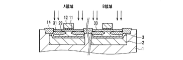
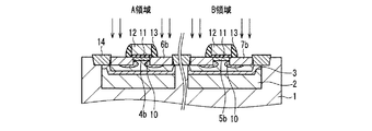
まず、本発明の実施の形態1に係る集積回路の構造について説明する。本実施の形態における集積回路は、エンハンスメント型とディプレッション型の、しきい値が異なる複数のトランジスタをそれぞれ有するアナログ/デジタル混載回路である。
本発明の実施の形態2に係る集積回路は、注入領域にドープする不純物を従来のトランジスタに比べて、重い不純物を用いることにより、拡散を抑え、変調度を改善し、変調度のばらつきを抑える。
2 pウェル領域
3 チャネルストップ領域
4a、4b、5a、5b 注入領域
6a、6b、7a、7b LDD領域
8a、8b、9a、9b ソース/ドレイン領域
10 ポケット注入領域
11 ゲート酸化膜
12 ゲート電極
13 サイドウォール絶縁膜
14 素子分離領域
21、22、24、28 レジスト
23、31、32 p型不純物層
25 n型不純物層
26 酸化膜
27 ポリシリコン
29 注入領域
33 不純物層
Claims (12)
- 第1導電型の半導体基板と、
前記半導体基板に形成され、ゲート電極の下にチャネル領域を有するエンハンスメント型MOSトランジスタおよびディプレッション型MOSトランジスタとを備え、
前記ディプレッション型MOSトランジスタの少なくとも1つには、前記ゲート電極側の前記チャネル領域に、前記半導体基板と同じ濃度の第1導電型の不純物、および逆導電型となる第2導電型の不純物を有する注入領域が形成され、
前記注入領域の第2導電型の不純物濃度は、前記第1導電型の不純物濃度より高いことを特徴とする集積回路。 - 前記チャネル領域内に、前記注入領域の下に形成された第1導電型のポケット注入領域を有し、
前記第2導電型の不純物は、前記ポケット注入領域よりも浅く注入されたことを特徴とする請求項1記載の集積回路。 - 前記チャネル領域に注入された第2導電型不純物は、リンである請求項2記載の集積回路。
- 前記チャネル領域に注入された第2導電型不純物は、砒素である請求項2記載の集積回路。
- 第1導電型の半導体基板と、
前記半導体基板に形成され、ゲート電極の下にチャネル領域を有するエンハンスメント型MOSトランジスタおよびディプレッション型MOSトランジスタとを備え、
前記ディプレッション型MOSトランジスタの少なくとも1つは、前記チャネル領域が、前記半導体基板より不純物濃度が高い前記第1導電型の不純物、および前記第1導電型不純物より濃度が高く、前記第1導電型と逆導電型となる第2導電型の不純物を有する注入領域と、
前記注入領域の下に形成された第1導電型のポケット注入領域とを有し、
前記第2導電型の不純物は、前記ポケット注入領域よりも浅く注入されたことを特徴とする集積回路。 - 前記第1導電型の不純物がボロンであり、前記第2導電型の不純物が砒素である請求項5記載の集積回路。
- 前記複数のディプレッション型MOSトランジスタには、他としきい値が異なるディプレッション型MOSトランジスタがある請求項1〜6のいずれか1項に記載の集積回路。
- 請求項1〜7のいずれか1項に記載の集積回路を備えた固体撮像装置。
- 第1導電型の半導体基板に形成されたエンハンスメント型MOSトランジスタおよびディプレッション型MOSトランジスタとを備えた集積回路の製造方法において、
前記ディプレッション型MOSトランジスタの少なくとも1つは、
前記半導体基板の表面に、前記第1導電型不純物と逆導電型の不純物である第2導電型の不純物を注入し、前記第2導電型として機能する注入領域を形成し、
前記注入領域上にゲート電極を形成し、
前記ゲート電極をマスクとして、前記半導体基板に第2導電型の不純物を注入して、ドレイン、ソース領域を形成することを特徴とする集積回路の製造方法。 - 前記ゲート電極を形成した後に、
前記ゲート電極をマスクとして、前記注入領域の下に、第1導電型の不純物を注入しポケット領域を形成する請求項9記載の集積回路の製造方法。 - 第1導電型の半導体基板と、前記半導体基板に形成されたエンハンスメント型MOSトランジスタおよびディプレッション型MOSトランジスタとを備えた集積回路の製造方法において、
前記ディプレッション型MOSトランジスタの少なくとも1つは、
前記半導体基板の表面に、第1導電型の不純物を注入し、
前記第1導電型の不純物が注入された半導体基板の表面に、前記第1導電型の不純物より重く、第1導電型と逆導電型である第2導電型半導体として機能する量の第2導電型の不純物を注入して注入領域を形成し、
前記注入領域上の一部にゲート電極を形成し、
前記ゲート電極をマスクとして、前記注入領域の下に、第1導電型の不純物を注入しポケット領域を形成し、
前記ゲート電極をマスクとして、上に前記ゲート電極が形成されていない前記注入領域に第2導電型の不純物を注入し、ドレイン、ソース領域を形成することを特徴とする集積回路の製造方法。 - 請求項9〜11のいずれか一項に記載の集積回路の製造方法を用いる固体撮像装置の製造方法。
Priority Applications (6)
| Application Number | Priority Date | Filing Date | Title |
|---|---|---|---|
| JP2005352396A JP2007158105A (ja) | 2005-12-06 | 2005-12-06 | 集積回路およびその製造方法 |
| TW095142498A TW200729498A (en) | 2005-12-06 | 2006-11-17 | Integrated circuit and method of manufacturing the same |
| US11/562,126 US7851867B2 (en) | 2005-12-06 | 2006-11-21 | Integrated circuit and method of manufacturing the same |
| KR1020060116129A KR20070059960A (ko) | 2005-12-06 | 2006-11-23 | 집적 회로 및 그 제조 방법 |
| CNA2006101640725A CN1979862A (zh) | 2005-12-06 | 2006-12-06 | 集成电路及其制造方法 |
| EP06256228A EP1796161A3 (en) | 2005-12-06 | 2006-12-06 | Integrated circuit and method of manufacturing the same |
Applications Claiming Priority (1)
| Application Number | Priority Date | Filing Date | Title |
|---|---|---|---|
| JP2005352396A JP2007158105A (ja) | 2005-12-06 | 2005-12-06 | 集積回路およびその製造方法 |
Publications (1)
| Publication Number | Publication Date |
|---|---|
| JP2007158105A true JP2007158105A (ja) | 2007-06-21 |
Family
ID=37845231
Family Applications (1)
| Application Number | Title | Priority Date | Filing Date |
|---|---|---|---|
| JP2005352396A Pending JP2007158105A (ja) | 2005-12-06 | 2005-12-06 | 集積回路およびその製造方法 |
Country Status (6)
| Country | Link |
|---|---|
| US (1) | US7851867B2 (ja) |
| EP (1) | EP1796161A3 (ja) |
| JP (1) | JP2007158105A (ja) |
| KR (1) | KR20070059960A (ja) |
| CN (1) | CN1979862A (ja) |
| TW (1) | TW200729498A (ja) |
Cited By (1)
| Publication number | Priority date | Publication date | Assignee | Title |
|---|---|---|---|---|
| JP2013229442A (ja) * | 2012-04-25 | 2013-11-07 | Sharp Corp | 半導体装置及びその製造方法 |
Families Citing this family (12)
| Publication number | Priority date | Publication date | Assignee | Title |
|---|---|---|---|---|
| US8354718B2 (en) * | 2007-05-22 | 2013-01-15 | Taiwan Semiconductor Manufacturing Company, Ltd. | Semiconductor device including an arrangement for suppressing short channel effects |
| KR100871792B1 (ko) * | 2007-06-26 | 2008-12-05 | 주식회사 동부하이텍 | 이미지센서 및 그 제조방법 |
| GB2451116A (en) * | 2007-07-20 | 2009-01-21 | X Fab Uk Ltd | Polysilicon devices |
| KR101631454B1 (ko) * | 2008-10-31 | 2016-06-17 | 가부시키가이샤 한도오따이 에네루기 켄큐쇼 | 논리회로 |
| JP2011129565A (ja) * | 2009-12-15 | 2011-06-30 | Elpida Memory Inc | 半導体装置およびその製造方法 |
| CN104008974A (zh) * | 2013-02-26 | 2014-08-27 | 中国科学院微电子研究所 | 半导体器件及其制造方法 |
| CN104916539B (zh) * | 2014-03-12 | 2018-08-21 | 中芯国际集成电路制造(上海)有限公司 | 一种制作半导体器件的方法 |
| CN103887961B (zh) * | 2014-04-18 | 2015-06-10 | 杭州士兰微电子股份有限公司 | 开关电源及其控制器 |
| JP2019033195A (ja) * | 2017-08-09 | 2019-02-28 | キヤノン株式会社 | 撮像装置の製造方法 |
| JP7009033B2 (ja) * | 2018-02-06 | 2022-01-25 | エイブリック株式会社 | 基準電圧発生装置 |
| CN112420752B (zh) * | 2019-08-20 | 2022-12-02 | 复旦大学 | 基于半导体衬底的新型单晶体管像素传感器及制备方法 |
| CN115995687B (zh) * | 2021-10-20 | 2026-03-31 | 群创光电股份有限公司 | 电子装置 |
Citations (11)
| Publication number | Priority date | Publication date | Assignee | Title |
|---|---|---|---|---|
| JPS5516480A (en) * | 1978-07-21 | 1980-02-05 | Nippon Telegr & Teleph Corp <Ntt> | Insulating gate electrostatic effect transistor and semiconductor integrated circuit device |
| JPS5586161A (en) * | 1978-12-23 | 1980-06-28 | Fujitsu Ltd | Manufacture of semiconductor device |
| JPS5660064A (en) * | 1979-10-23 | 1981-05-23 | Fujitsu Ltd | Manufacture of semiconductor device |
| JPS58134475A (ja) * | 1982-02-05 | 1983-08-10 | Toshiba Corp | 半導体集積回路 |
| JPH06236967A (ja) * | 1992-12-14 | 1994-08-23 | Toshiba Corp | 半導体装置の製造方法 |
| JPH07130891A (ja) * | 1993-11-02 | 1995-05-19 | Sony Corp | 半導体装置の製造方法 |
| JPH07297295A (ja) * | 1994-04-20 | 1995-11-10 | Sony Corp | Mosトランジスタ構造およびこれを用いた電荷転送装置 |
| JPH11307650A (ja) * | 1998-02-17 | 1999-11-05 | Seiko Instruments Inc | 半導体装置 |
| JPH11330264A (ja) * | 1998-05-12 | 1999-11-30 | Hitachi Ltd | 半導体集積回路装置およびその製造方法 |
| JP2000188391A (ja) * | 1997-12-24 | 2000-07-04 | Seiko Instruments Inc | 半導体集積回路装置の製造方法 |
| JP2003031678A (ja) * | 2001-07-16 | 2003-01-31 | Fuji Electric Co Ltd | Mos基準電圧回路およびその製造方法 |
Family Cites Families (13)
| Publication number | Priority date | Publication date | Assignee | Title |
|---|---|---|---|---|
| JPS60134468A (ja) | 1983-12-23 | 1985-07-17 | Hitachi Ltd | 半導体装置 |
| US5770485A (en) * | 1997-03-04 | 1998-06-23 | Advanced Micro Devices, Inc. | MOSFET device with an amorphized source and fabrication method thereof |
| US5976956A (en) | 1997-04-11 | 1999-11-02 | Advanced Micro Devices, Inc. | Method of controlling dopant concentrations using transient-enhanced diffusion prior to gate formation in a device |
| US5885874A (en) | 1997-04-21 | 1999-03-23 | Advanced Micro Devices, Inc. | Method of making enhancement-mode and depletion-mode IGFETS using selective doping of a gate material |
| US6093951A (en) * | 1997-06-30 | 2000-07-25 | Sun Microsystems, Inc. | MOS devices with retrograde pocket regions |
| JP4326606B2 (ja) * | 1998-03-26 | 2009-09-09 | 株式会社ルネサステクノロジ | 半導体装置およびその製造方法 |
| JPH11354785A (ja) | 1998-06-10 | 1999-12-24 | Hitachi Ltd | 電界効果トランジスタ、それを有する半導体集積回路装置およびその製造方法 |
| JP2000323587A (ja) | 1999-05-10 | 2000-11-24 | Nikon Corp | Cmos半導体装置及びその製造方法 |
| US6268256B1 (en) * | 2000-01-18 | 2001-07-31 | United Microelectronics Corp. | Method for reducing short channel effect |
| US20020058385A1 (en) * | 2000-10-26 | 2002-05-16 | Taiji Noda | Semiconductor device and method for manufacturing the same |
| JP2002151599A (ja) | 2000-11-13 | 2002-05-24 | Hitachi Ltd | 半導体集積回路装置およびその製造方法 |
| US20040005763A1 (en) * | 2000-12-05 | 2004-01-08 | United Microelectronics Corp. | Method of manufacturing low-leakage, high-performance device |
| US20040033469A1 (en) * | 2002-08-15 | 2004-02-19 | Blacklock Gordon D. | Dental implant anchor having internal/external wrench engaging means |
-
2005
- 2005-12-06 JP JP2005352396A patent/JP2007158105A/ja active Pending
-
2006
- 2006-11-17 TW TW095142498A patent/TW200729498A/zh unknown
- 2006-11-21 US US11/562,126 patent/US7851867B2/en active Active
- 2006-11-23 KR KR1020060116129A patent/KR20070059960A/ko not_active Withdrawn
- 2006-12-06 EP EP06256228A patent/EP1796161A3/en not_active Withdrawn
- 2006-12-06 CN CNA2006101640725A patent/CN1979862A/zh active Pending
Patent Citations (11)
| Publication number | Priority date | Publication date | Assignee | Title |
|---|---|---|---|---|
| JPS5516480A (en) * | 1978-07-21 | 1980-02-05 | Nippon Telegr & Teleph Corp <Ntt> | Insulating gate electrostatic effect transistor and semiconductor integrated circuit device |
| JPS5586161A (en) * | 1978-12-23 | 1980-06-28 | Fujitsu Ltd | Manufacture of semiconductor device |
| JPS5660064A (en) * | 1979-10-23 | 1981-05-23 | Fujitsu Ltd | Manufacture of semiconductor device |
| JPS58134475A (ja) * | 1982-02-05 | 1983-08-10 | Toshiba Corp | 半導体集積回路 |
| JPH06236967A (ja) * | 1992-12-14 | 1994-08-23 | Toshiba Corp | 半導体装置の製造方法 |
| JPH07130891A (ja) * | 1993-11-02 | 1995-05-19 | Sony Corp | 半導体装置の製造方法 |
| JPH07297295A (ja) * | 1994-04-20 | 1995-11-10 | Sony Corp | Mosトランジスタ構造およびこれを用いた電荷転送装置 |
| JP2000188391A (ja) * | 1997-12-24 | 2000-07-04 | Seiko Instruments Inc | 半導体集積回路装置の製造方法 |
| JPH11307650A (ja) * | 1998-02-17 | 1999-11-05 | Seiko Instruments Inc | 半導体装置 |
| JPH11330264A (ja) * | 1998-05-12 | 1999-11-30 | Hitachi Ltd | 半導体集積回路装置およびその製造方法 |
| JP2003031678A (ja) * | 2001-07-16 | 2003-01-31 | Fuji Electric Co Ltd | Mos基準電圧回路およびその製造方法 |
Cited By (1)
| Publication number | Priority date | Publication date | Assignee | Title |
|---|---|---|---|---|
| JP2013229442A (ja) * | 2012-04-25 | 2013-11-07 | Sharp Corp | 半導体装置及びその製造方法 |
Also Published As
| Publication number | Publication date |
|---|---|
| US20070228495A1 (en) | 2007-10-04 |
| US7851867B2 (en) | 2010-12-14 |
| TW200729498A (en) | 2007-08-01 |
| KR20070059960A (ko) | 2007-06-12 |
| EP1796161A3 (en) | 2009-03-04 |
| EP1796161A2 (en) | 2007-06-13 |
| CN1979862A (zh) | 2007-06-13 |
Similar Documents
| Publication | Publication Date | Title |
|---|---|---|
| US7592241B2 (en) | Semiconductor device having well with peak impurity concentrations and method for fabricating the same | |
| US20020005552A1 (en) | Semiconductor device having different field oxide sizes | |
| US20050082573A1 (en) | Threshold voltage adjustment for long channel transistors | |
| JPH09270466A (ja) | 半導体装置及びその製造方法 | |
| US5891782A (en) | Method for fabricating an asymmetric channel doped MOS structure | |
| US20080283922A1 (en) | Semiconductor device and manufacturing method thereof | |
| KR100391959B1 (ko) | 반도체 장치 및 제조 방법 | |
| JP2007158105A (ja) | 集積回路およびその製造方法 | |
| JP3015253B2 (ja) | 半導体装置およびその製造方法 | |
| KR100302648B1 (ko) | 반도체장치및그제조방법 | |
| KR101781220B1 (ko) | 디프레션형 mos 트랜지스터를 갖는 반도체 장치 | |
| US5786265A (en) | Methods of forming integrated semiconductor devices having improved channel-stop regions therein, and devices formed thereby | |
| KR0159141B1 (ko) | 다수의 불순물층을 포함하고 있는 반도체장치 및 그 제조방법 | |
| US7015554B2 (en) | Semiconductor device and method for fabricating the same | |
| KR100496244B1 (ko) | 반도체 장치 및 그 제조 방법 | |
| JP2001284540A (ja) | 半導体装置およびその製造方法 | |
| JP3744438B2 (ja) | 半導体装置 | |
| US20100320570A1 (en) | Semiconductor device | |
| US7554163B2 (en) | Semiconductor device | |
| KR100254642B1 (ko) | 반도체 장치 및 그 제조 방법 | |
| JPH1012870A (ja) | 半導体装置及びその製造方法 | |
| KR100587605B1 (ko) | 고전압 트랜지스터 및 그 제조방법 | |
| US20250366021A1 (en) | Pdsoi transistor and method for fabricating same | |
| JP2004221223A (ja) | Mis型半導体装置及びその製造方法 | |
| KR100574357B1 (ko) | 벌크 펀치쓰루우를 억제하기 위한 모스 트랜지스터 |
Legal Events
| Date | Code | Title | Description |
|---|---|---|---|
| A621 | Written request for application examination |
Free format text: JAPANESE INTERMEDIATE CODE: A621 Effective date: 20080623 |
|
| A977 | Report on retrieval |
Free format text: JAPANESE INTERMEDIATE CODE: A971007 Effective date: 20101015 |
|
| A131 | Notification of reasons for refusal |
Free format text: JAPANESE INTERMEDIATE CODE: A131 Effective date: 20101021 |
|
| A521 | Request for written amendment filed |
Free format text: JAPANESE INTERMEDIATE CODE: A523 Effective date: 20101210 |
|
| A02 | Decision of refusal |
Free format text: JAPANESE INTERMEDIATE CODE: A02 Effective date: 20110208 |