JP2007189201A - 窒化物半導体発光素子および窒化物半導体レーザ素子の製造方法 - Google Patents
窒化物半導体発光素子および窒化物半導体レーザ素子の製造方法 Download PDFInfo
- Publication number
- JP2007189201A JP2007189201A JP2006320327A JP2006320327A JP2007189201A JP 2007189201 A JP2007189201 A JP 2007189201A JP 2006320327 A JP2006320327 A JP 2006320327A JP 2006320327 A JP2006320327 A JP 2006320327A JP 2007189201 A JP2007189201 A JP 2007189201A
- Authority
- JP
- Japan
- Prior art keywords
- nitride semiconductor
- film
- light emitting
- oxynitride
- semiconductor laser
- Prior art date
- Legal status (The legal status is an assumption and is not a legal conclusion. Google has not performed a legal analysis and makes no representation as to the accuracy of the status listed.)
- Granted
Links
Images




Classifications
-
- H—ELECTRICITY
- H01—ELECTRIC ELEMENTS
- H01S—DEVICES USING THE PROCESS OF LIGHT AMPLIFICATION BY STIMULATED EMISSION OF RADIATION [LASER] TO AMPLIFY OR GENERATE LIGHT; DEVICES USING STIMULATED EMISSION OF ELECTROMAGNETIC RADIATION IN WAVE RANGES OTHER THAN OPTICAL
- H01S5/00—Semiconductor lasers
- H01S5/30—Structure or shape of the active region; Materials used for the active region
- H01S5/34—Structure or shape of the active region; Materials used for the active region comprising quantum well or superlattice structures, e.g. single quantum well [SQW] lasers, multiple quantum well [MQW] lasers or graded index separate confinement heterostructure [GRINSCH] lasers
- H01S5/343—Structure or shape of the active region; Materials used for the active region comprising quantum well or superlattice structures, e.g. single quantum well [SQW] lasers, multiple quantum well [MQW] lasers or graded index separate confinement heterostructure [GRINSCH] lasers in AIIIBV compounds, e.g. AlGaAs-laser, InP-based laser
- H01S5/34333—Structure or shape of the active region; Materials used for the active region comprising quantum well or superlattice structures, e.g. single quantum well [SQW] lasers, multiple quantum well [MQW] lasers or graded index separate confinement heterostructure [GRINSCH] lasers in AIIIBV compounds, e.g. AlGaAs-laser, InP-based laser with a well layer based on Ga(In)N or Ga(In)P, e.g. blue laser
-
- H—ELECTRICITY
- H01—ELECTRIC ELEMENTS
- H01S—DEVICES USING THE PROCESS OF LIGHT AMPLIFICATION BY STIMULATED EMISSION OF RADIATION [LASER] TO AMPLIFY OR GENERATE LIGHT; DEVICES USING STIMULATED EMISSION OF ELECTROMAGNETIC RADIATION IN WAVE RANGES OTHER THAN OPTICAL
- H01S5/00—Semiconductor lasers
-
- B—PERFORMING OPERATIONS; TRANSPORTING
- B82—NANOTECHNOLOGY
- B82Y—SPECIFIC USES OR APPLICATIONS OF NANOSTRUCTURES; MEASUREMENT OR ANALYSIS OF NANOSTRUCTURES; MANUFACTURE OR TREATMENT OF NANOSTRUCTURES
- B82Y20/00—Nanooptics, e.g. quantum optics or photonic crystals
-
- H—ELECTRICITY
- H01—ELECTRIC ELEMENTS
- H01S—DEVICES USING THE PROCESS OF LIGHT AMPLIFICATION BY STIMULATED EMISSION OF RADIATION [LASER] TO AMPLIFY OR GENERATE LIGHT; DEVICES USING STIMULATED EMISSION OF ELECTROMAGNETIC RADIATION IN WAVE RANGES OTHER THAN OPTICAL
- H01S5/00—Semiconductor lasers
- H01S5/02—Structural details or components not essential to laser action
- H01S5/028—Coatings ; Treatment of the laser facets, e.g. etching, passivation layers or reflecting layers
-
- H—ELECTRICITY
- H01—ELECTRIC ELEMENTS
- H01S—DEVICES USING THE PROCESS OF LIGHT AMPLIFICATION BY STIMULATED EMISSION OF RADIATION [LASER] TO AMPLIFY OR GENERATE LIGHT; DEVICES USING STIMULATED EMISSION OF ELECTROMAGNETIC RADIATION IN WAVE RANGES OTHER THAN OPTICAL
- H01S5/00—Semiconductor lasers
- H01S5/20—Structure or shape of the semiconductor body to guide the optical wave ; Confining structures perpendicular to the optical axis, e.g. index or gain guiding, stripe geometry, broad area lasers, gain tailoring, transverse or lateral reflectors, special cladding structures, MQW barrier reflection layers
- H01S5/2036—Broad area lasers
-
- H—ELECTRICITY
- H01—ELECTRIC ELEMENTS
- H01S—DEVICES USING THE PROCESS OF LIGHT AMPLIFICATION BY STIMULATED EMISSION OF RADIATION [LASER] TO AMPLIFY OR GENERATE LIGHT; DEVICES USING STIMULATED EMISSION OF ELECTROMAGNETIC RADIATION IN WAVE RANGES OTHER THAN OPTICAL
- H01S5/00—Semiconductor lasers
- H01S5/20—Structure or shape of the semiconductor body to guide the optical wave ; Confining structures perpendicular to the optical axis, e.g. index or gain guiding, stripe geometry, broad area lasers, gain tailoring, transverse or lateral reflectors, special cladding structures, MQW barrier reflection layers
- H01S5/22—Structure or shape of the semiconductor body to guide the optical wave ; Confining structures perpendicular to the optical axis, e.g. index or gain guiding, stripe geometry, broad area lasers, gain tailoring, transverse or lateral reflectors, special cladding structures, MQW barrier reflection layers having a ridge or stripe structure
-
- H—ELECTRICITY
- H10—SEMICONDUCTOR DEVICES; ELECTRIC SOLID-STATE DEVICES NOT OTHERWISE PROVIDED FOR
- H10H—INORGANIC LIGHT-EMITTING SEMICONDUCTOR DEVICES HAVING POTENTIAL BARRIERS
- H10H20/00—Individual inorganic light-emitting semiconductor devices having potential barriers, e.g. light-emitting diodes [LED]
- H10H20/80—Constructional details
- H10H20/84—Coatings, e.g. passivation layers or antireflective coatings
Landscapes
- Physics & Mathematics (AREA)
- Optics & Photonics (AREA)
- Condensed Matter Physics & Semiconductors (AREA)
- General Physics & Mathematics (AREA)
- Electromagnetism (AREA)
- Engineering & Computer Science (AREA)
- Nanotechnology (AREA)
- Chemical & Material Sciences (AREA)
- Biophysics (AREA)
- Crystallography & Structural Chemistry (AREA)
- Life Sciences & Earth Sciences (AREA)
- Semiconductor Lasers (AREA)
- Physical Vapour Deposition (AREA)
- Formation Of Insulating Films (AREA)
Abstract
【解決手段】光出射部にコート膜が形成されている窒化物半導体発光素子であって、光出射部は窒化物半導体からなり、光出射部に接するコート膜が酸窒化物からなる窒化物半導体発光素子である。また、共振器端面にコート膜が形成されている窒化物半導体レーザ素子を製造する方法であって、劈開により共振器端面を形成する工程と、共振器端面に酸窒化物からなるコート膜を形成する工程と、を含む、窒化物半導体レーザ素子の製造方法である。
【選択図】図1
Description
ここで、窒化物からなる膜がシリコンの窒化物からなる膜である場合には、そのシリコンの窒化物からなる膜の厚さは5nm以上であることが好ましい。

アルミニウムからなるターゲットが設置してある反応性スパッタリング装置の成膜室内に酸素ガスを導入し、マイクロ波を印加して、アルミニウムからなるターゲットを酸素プラズマに曝すことにより、アルミニウムからなるターゲットの表面から数nm程度酸化させ、酸化アルミニウムからなるターゲットを形成する。
その後、成膜室内に窒素ガスとアルゴンガスとを導入し、マイクロ波を印加してプラズマ状態にして、酸化アルミニウムからなるターゲットをスパッタリングすることにより、アルミニウムの酸窒化物を形成することが可能となる。
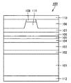
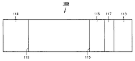
図1に、本実施の形態の窒化物半導体レーザ素子の好ましい一例の模式的な断面図を示す。ここで、本実施の形態の窒化物半導体レーザ素子100は、n型GaN基板101上に、n型AlGaInNバッファ層102、n型AlGaInNクラッド層103、n型AlGaInNガイド層104、AlGaInN多重量子井戸活性層105、p型AlGaInNガイド層106、p型AlGaInNクラッド層107およびp型AlGaInNコンタクト層108がn型GaN基板101側からこの順序で積層された構成を有している。なお、上記の各層の混晶比は適宜調節されるものであり、本発明の本質とは関係がない。また、本実施の形態の窒化物半導体レーザ素子から発振されるレーザ光の波長はAlGaInN多重量子井戸活性層105の混晶比によって、たとえば370nm〜470nmの範囲で適宜調節することができる。本実施の形態においては、405nmの波長のレーザ光が発振するように調節された。
本実施の形態の窒化物半導体レーザ素子は、光出射側の共振器端面に形成されるコート膜の構成および光反射側の共振器端面に形成される膜の構成を変更したこと以外は、実施の形態1の窒化物半導体レーザ素子と同様の構成を有している。
本実施の形態の窒化物半導体レーザ素子は、光出射側の共振器端面に形成されるコート膜の構成および光反射側の共振器端面に形成される膜の構成を変更したこと以外は、実施の形態1の窒化物半導体レーザ素子と同様の構成を有している。
本実施の形態の窒化物半導体レーザ素子は、光出射側の共振器端面に形成されるコート膜の構成および光反射側の共振器端面に形成される膜の構成を変更したこと以外は、実施の形態1の窒化物半導体レーザ素子と同様の構成を有している。
本実施の形態の窒化物半導体レーザ素子は、460nmの波長のレーザ光が発振するように調節されたこと、ならびに光出射側の共振器端面に形成されるコート膜の構成および光反射側の共振器端面に形成される膜の構成を変更したこと以外は、実施の形態1の窒化物半導体レーザ素子と同様の構成を有している。なお、発振されるレーザ光の波長は、AlGaInN多重量子井戸活性層のAlGaInNの混晶比を変更することで調節している。
本実施の形態の窒化物半導体レーザ素子は、光出射側の共振器端面に形成されるコート膜の構成および光反射側の共振器端面に形成される膜の構成を変更したこと以外は、実施の形態1の窒化物半導体レーザ素子と同様の構成を有している。
本実施の形態の窒化物半導体レーザ素子は、光出射側の共振器端面に形成されるコート膜の構成および光反射側の共振器端面に形成される膜の構成を変更したこと以外は、実施の形態1の窒化物半導体レーザ素子と同様の構成を有している。
Claims (15)
- 光出射部にコート膜が形成されている窒化物半導体発光素子であって、前記光出射部は窒化物半導体からなり、前記光出射部に接するコート膜が酸窒化物からなることを特徴とする、窒化物半導体発光素子。
- 前記窒化物半導体発光素子は窒化物半導体レーザ素子であって、前記光出射部は共振器端面であることを特徴とする、請求項1に記載の窒化物半導体発光素子。
- 前記酸窒化物は、アルミニウムの酸窒化物またはシリコンの酸窒化物であることを特徴とする、請求項1または2に記載の窒化物半導体発光素子。
- 前記酸窒化物中の酸素の含有量が2原子%以上35原子%以下であることを特徴とする、請求項1から3のいずれかに記載の窒化物半導体発光素子。
- 前記酸窒化物中の酸素の含有量が2原子%以上15原子%以下であることを特徴とする、請求項1から3のいずれかに記載の窒化物半導体発光素子。
- 前記コート膜上に酸化物または窒化物からなる膜が形成されていることを特徴とする、請求項1から5のいずれかに記載の窒化物半導体発光素子。
- 前記窒化物からなる膜がシリコンおよびアルミニウムの少なくとも一方の窒化物からなる膜であることを特徴とする、請求項6に記載の窒化物半導体発光素子。
- 前記窒化物からなる膜がシリコンの窒化物からなる膜であり、前記シリコンの窒化物からなる膜の厚さが5nm以上であることを特徴とする、請求項7に記載の窒化物半導体発光素子。
- 前記酸化物からなる膜が酸化アルミニウム、酸化シリコン、酸化チタン、酸化ハフニウム、酸化ジルコニウム、酸化ニオブ、酸化タンタルおよび酸化イットリウムからなる群から選択された少なくとも1種の膜であることを特徴とする、請求項6に記載の窒化物半導体発光素子。
- 前記コート膜上に酸窒化物からなる膜が形成されていることを特徴とする、請求項1に記載の窒化物半導体発光素子。
- 前記酸窒化物からなる膜がシリコンまたはアルミニウムの酸窒化物からなる膜であることを特徴とする、請求項10に記載の窒化物半導体発光素子。
- 前記コート膜上にフッ化マグネシウムからなる膜が形成されていることを特徴とする、請求項1に記載の窒化物半導体発光素子。
- 共振器端面にコート膜が形成されている窒化物半導体レーザ素子を製造する方法であって、劈開により前記共振器端面を形成する工程と、前記共振器端面に酸窒化物からなるコート膜を形成する工程と、を含む、窒化物半導体レーザ素子の製造方法。
- 前記酸窒化物は、ターゲットに酸化アルミニウムを用いて作製されたことを特徴とする請求項13に記載の窒化物半導体レーザ素子の製造方法。
- 前記酸窒化物は、ターゲットにアルミニウムの酸窒化物を用いて作製されたことを特徴とする請求項13に記載の窒化物半導体レーザ素子の製造方法。
Priority Applications (12)
| Application Number | Priority Date | Filing Date | Title |
|---|---|---|---|
| JP2006320327A JP5191650B2 (ja) | 2005-12-16 | 2006-11-28 | 窒化物半導体発光素子および窒化物半導体発光素子の製造方法 |
| KR1020060122938A KR100829137B1 (ko) | 2005-12-16 | 2006-12-06 | 질화물반도체 발광 소자 및 질화물반도체 레이저 소자의제조 방법 |
| US11/638,582 US8368095B2 (en) | 2005-12-16 | 2006-12-14 | Nitride semiconductor light emitting device and method of fabricating nitride semiconductor laser device |
| CN2010105102836A CN102005699A (zh) | 2005-12-16 | 2006-12-15 | 氮化物半导体发光元件及氮化物半导体激光元件的制造方法 |
| CN2011101196059A CN102231477A (zh) | 2005-12-16 | 2006-12-15 | 氮化物半导体发光元件及氮化物半导体激光元件的制造方法 |
| CN2006101717110A CN1983748B (zh) | 2005-12-16 | 2006-12-15 | 氮化物半导体发光元件及氮化物半导体激光元件的制造方法 |
| KR1020080007919A KR100868268B1 (ko) | 2005-12-16 | 2008-01-25 | 질화물반도체 발광 소자 및 질화물반도체 레이저 소자의제조 방법 |
| US12/153,756 US8735192B2 (en) | 2005-12-16 | 2008-05-23 | Nitride semiconductor light emitting device and method of fabricating nitride semiconductor laser device |
| KR1020080050232A KR100898958B1 (ko) | 2005-12-16 | 2008-05-29 | 질화물반도체 발광 소자 및 질화물반도체 레이저 소자의제조 방법 |
| KR1020080108970A KR100924498B1 (ko) | 2005-12-16 | 2008-11-04 | 질화물반도체 발광 소자 및 질화물반도체 레이저 소자의 제조 방법 |
| KR1020080108978A KR100924500B1 (ko) | 2005-12-16 | 2008-11-04 | 질화물반도체 발광 소자 및 질화물반도체 레이저 소자의 제조 방법 |
| US12/382,530 US20090218593A1 (en) | 2005-12-16 | 2009-03-18 | Nitride semiconductor light emitting device and method of frabicating nitride semiconductor laser device |
Applications Claiming Priority (3)
| Application Number | Priority Date | Filing Date | Title |
|---|---|---|---|
| JP2005363590 | 2005-12-16 | ||
| JP2005363590 | 2005-12-16 | ||
| JP2006320327A JP5191650B2 (ja) | 2005-12-16 | 2006-11-28 | 窒化物半導体発光素子および窒化物半導体発光素子の製造方法 |
Related Child Applications (1)
| Application Number | Title | Priority Date | Filing Date |
|---|---|---|---|
| JP2012145435A Division JP5766659B2 (ja) | 2005-12-16 | 2012-06-28 | 窒化物半導体発光素子 |
Publications (3)
| Publication Number | Publication Date |
|---|---|
| JP2007189201A true JP2007189201A (ja) | 2007-07-26 |
| JP2007189201A5 JP2007189201A5 (ja) | 2010-01-21 |
| JP5191650B2 JP5191650B2 (ja) | 2013-05-08 |
Family
ID=38172436
Family Applications (1)
| Application Number | Title | Priority Date | Filing Date |
|---|---|---|---|
| JP2006320327A Active JP5191650B2 (ja) | 2005-12-16 | 2006-11-28 | 窒化物半導体発光素子および窒化物半導体発光素子の製造方法 |
Country Status (4)
| Country | Link |
|---|---|
| US (3) | US8368095B2 (ja) |
| JP (1) | JP5191650B2 (ja) |
| KR (5) | KR100829137B1 (ja) |
| CN (3) | CN102231477A (ja) |
Cited By (6)
| Publication number | Priority date | Publication date | Assignee | Title |
|---|---|---|---|---|
| JP2009194150A (ja) * | 2008-02-14 | 2009-08-27 | Sharp Corp | 窒化物半導体発光素子 |
| US7792172B2 (en) | 2007-10-04 | 2010-09-07 | Sharp Kabushiki Kaisha | Nitride semiconductor laser device |
| US7970035B2 (en) | 2008-03-19 | 2011-06-28 | Sharp Kabushiki Kaisha | Nitride semiconductor laser element and external-cavity semiconductor laser device |
| US8368098B2 (en) | 2007-06-05 | 2013-02-05 | Sharp Kabushiki Kaisha | Light emitting device and manufacturing method thereof |
| US8571083B2 (en) | 2009-06-11 | 2013-10-29 | Sharp Kabushiki Kaisha | Nitride semiconductor laser chip |
| WO2018139528A1 (ja) * | 2017-01-26 | 2018-08-02 | 株式会社 アルバック | 酸化アルミニウム膜の形成方法 |
Families Citing this family (134)
| Publication number | Priority date | Publication date | Assignee | Title |
|---|---|---|---|---|
| US7707603B2 (en) * | 2005-01-28 | 2010-04-27 | Microsoft Corporation | Digital media transfer based on user behavior |
| JP5191650B2 (ja) * | 2005-12-16 | 2013-05-08 | シャープ株式会社 | 窒化物半導体発光素子および窒化物半導体発光素子の製造方法 |
| KR100853241B1 (ko) * | 2005-12-16 | 2008-08-20 | 샤프 가부시키가이샤 | 질화물 반도체 발광소자 및 질화물 반도체 레이저 소자의제조방법 |
| JP2008060472A (ja) * | 2006-09-01 | 2008-03-13 | Sumitomo Electric Ind Ltd | 半導体レーザ及びその製造方法 |
| US8097081B2 (en) | 2008-06-05 | 2012-01-17 | Soraa, Inc. | High pressure apparatus and method for nitride crystal growth |
| US8871024B2 (en) | 2008-06-05 | 2014-10-28 | Soraa, Inc. | High pressure apparatus and method for nitride crystal growth |
| US9157167B1 (en) | 2008-06-05 | 2015-10-13 | Soraa, Inc. | High pressure apparatus and method for nitride crystal growth |
| US8847249B2 (en) | 2008-06-16 | 2014-09-30 | Soraa, Inc. | Solid-state optical device having enhanced indium content in active regions |
| US8303710B2 (en) * | 2008-06-18 | 2012-11-06 | Soraa, Inc. | High pressure apparatus and method for nitride crystal growth |
| US9404197B2 (en) | 2008-07-07 | 2016-08-02 | Soraa, Inc. | Large area, low-defect gallium-containing nitride crystals, method of making, and method of use |
| WO2011044554A1 (en) | 2009-10-09 | 2011-04-14 | Soraa, Inc. | Method for synthesis of high quality large area bulk gallium based crystals |
| US8143148B1 (en) | 2008-07-14 | 2012-03-27 | Soraa, Inc. | Self-aligned multi-dielectric-layer lift off process for laser diode stripes |
| US8805134B1 (en) | 2012-02-17 | 2014-08-12 | Soraa Laser Diode, Inc. | Methods and apparatus for photonic integration in non-polar and semi-polar oriented wave-guided optical devices |
| US8259769B1 (en) | 2008-07-14 | 2012-09-04 | Soraa, Inc. | Integrated total internal reflectors for high-gain laser diodes with high quality cleaved facets on nonpolar/semipolar GaN substrates |
| US8284810B1 (en) | 2008-08-04 | 2012-10-09 | Soraa, Inc. | Solid state laser device using a selected crystal orientation in non-polar or semi-polar GaN containing materials and methods |
| US8124996B2 (en) | 2008-08-04 | 2012-02-28 | Soraa, Inc. | White light devices using non-polar or semipolar gallium containing materials and phosphors |
| US8323405B2 (en) | 2008-08-07 | 2012-12-04 | Soraa, Inc. | Process and apparatus for growing a crystalline gallium-containing nitride using an azide mineralizer |
| US10036099B2 (en) | 2008-08-07 | 2018-07-31 | Slt Technologies, Inc. | Process for large-scale ammonothermal manufacturing of gallium nitride boules |
| US8021481B2 (en) | 2008-08-07 | 2011-09-20 | Soraa, Inc. | Process and apparatus for large-scale manufacturing of bulk monocrystalline gallium-containing nitride |
| US8430958B2 (en) | 2008-08-07 | 2013-04-30 | Soraa, Inc. | Apparatus and method for seed crystal utilization in large-scale manufacturing of gallium nitride |
| US20100031873A1 (en) * | 2008-08-07 | 2010-02-11 | Soraa, Inc. | Basket process and apparatus for crystalline gallium-containing nitride |
| US8979999B2 (en) | 2008-08-07 | 2015-03-17 | Soraa, Inc. | Process for large-scale ammonothermal manufacturing of gallium nitride boules |
| US7976630B2 (en) | 2008-09-11 | 2011-07-12 | Soraa, Inc. | Large-area seed for ammonothermal growth of bulk gallium nitride and method of manufacture |
| US8354679B1 (en) | 2008-10-02 | 2013-01-15 | Soraa, Inc. | Microcavity light emitting diode method of manufacture |
| US8455894B1 (en) | 2008-10-17 | 2013-06-04 | Soraa, Inc. | Photonic-crystal light emitting diode and method of manufacture |
| JP5221279B2 (ja) * | 2008-10-22 | 2013-06-26 | 株式会社ディスコ | 積層デバイスの製造方法 |
| US8000366B2 (en) * | 2008-11-21 | 2011-08-16 | Palo Alto Research Center Incorporated | Laser diode with high indium active layer and lattice matched cladding layer |
| US8878230B2 (en) | 2010-03-11 | 2014-11-04 | Soraa, Inc. | Semi-insulating group III metal nitride and method of manufacture |
| US8461071B2 (en) | 2008-12-12 | 2013-06-11 | Soraa, Inc. | Polycrystalline group III metal nitride with getter and method of making |
| US9543392B1 (en) | 2008-12-12 | 2017-01-10 | Soraa, Inc. | Transparent group III metal nitride and method of manufacture |
| US9589792B2 (en) | 2012-11-26 | 2017-03-07 | Soraa, Inc. | High quality group-III metal nitride crystals, methods of making, and methods of use |
| US8987156B2 (en) | 2008-12-12 | 2015-03-24 | Soraa, Inc. | Polycrystalline group III metal nitride with getter and method of making |
| US20100147210A1 (en) * | 2008-12-12 | 2010-06-17 | Soraa, Inc. | high pressure apparatus and method for nitride crystal growth |
| USRE47114E1 (en) | 2008-12-12 | 2018-11-06 | Slt Technologies, Inc. | Polycrystalline group III metal nitride with getter and method of making |
| US8247886B1 (en) | 2009-03-09 | 2012-08-21 | Soraa, Inc. | Polarization direction of optical devices using selected spatial configurations |
| US8422525B1 (en) | 2009-03-28 | 2013-04-16 | Soraa, Inc. | Optical device structure using miscut GaN substrates for laser applications |
| US8299473B1 (en) | 2009-04-07 | 2012-10-30 | Soraa, Inc. | Polarized white light devices using non-polar or semipolar gallium containing materials and transparent phosphors |
| US8634442B1 (en) | 2009-04-13 | 2014-01-21 | Soraa Laser Diode, Inc. | Optical device structure using GaN substrates for laser applications |
| US8242522B1 (en) | 2009-05-12 | 2012-08-14 | Soraa, Inc. | Optical device structure using non-polar GaN substrates and growth structures for laser applications in 481 nm |
| DE112010001615T5 (de) * | 2009-04-13 | 2012-08-02 | Soraa, Inc. | Stuktur eines optischen Elements unter Verwendung von GaN-Substraten für Laseranwendungen |
| US8294179B1 (en) | 2009-04-17 | 2012-10-23 | Soraa, Inc. | Optical device structure using GaN substrates and growth structures for laser applications |
| US8254425B1 (en) * | 2009-04-17 | 2012-08-28 | Soraa, Inc. | Optical device structure using GaN substrates and growth structures for laser applications |
| US8837545B2 (en) | 2009-04-13 | 2014-09-16 | Soraa Laser Diode, Inc. | Optical device structure using GaN substrates and growth structures for laser applications |
| US8416825B1 (en) | 2009-04-17 | 2013-04-09 | Soraa, Inc. | Optical device structure using GaN substrates and growth structure for laser applications |
| US8306081B1 (en) * | 2009-05-27 | 2012-11-06 | Soraa, Inc. | High indium containing InGaN substrates for long wavelength optical devices |
| US8247887B1 (en) | 2009-05-29 | 2012-08-21 | Soraa, Inc. | Method and surface morphology of non-polar gallium nitride containing substrates |
| US9250044B1 (en) | 2009-05-29 | 2016-02-02 | Soraa Laser Diode, Inc. | Gallium and nitrogen containing laser diode dazzling devices and methods of use |
| US9829780B2 (en) | 2009-05-29 | 2017-11-28 | Soraa Laser Diode, Inc. | Laser light source for a vehicle |
| US8509275B1 (en) | 2009-05-29 | 2013-08-13 | Soraa, Inc. | Gallium nitride based laser dazzling device and method |
| US10108079B2 (en) | 2009-05-29 | 2018-10-23 | Soraa Laser Diode, Inc. | Laser light source for a vehicle |
| US8427590B2 (en) | 2009-05-29 | 2013-04-23 | Soraa, Inc. | Laser based display method and system |
| US9800017B1 (en) | 2009-05-29 | 2017-10-24 | Soraa Laser Diode, Inc. | Laser device and method for a vehicle |
| JP2010278335A (ja) * | 2009-05-29 | 2010-12-09 | Sanyo Electric Co Ltd | 半導体レーザ素子及びこれを用いた光ピックアップ装置 |
| US8314429B1 (en) | 2009-09-14 | 2012-11-20 | Soraa, Inc. | Multi color active regions for white light emitting diode |
| US8750342B1 (en) | 2011-09-09 | 2014-06-10 | Soraa Laser Diode, Inc. | Laser diodes with scribe structures |
| US8355418B2 (en) | 2009-09-17 | 2013-01-15 | Soraa, Inc. | Growth structures and method for forming laser diodes on {20-21} or off cut gallium and nitrogen containing substrates |
| US8933644B2 (en) | 2009-09-18 | 2015-01-13 | Soraa, Inc. | LED lamps with improved quality of light |
| US9293644B2 (en) | 2009-09-18 | 2016-03-22 | Soraa, Inc. | Power light emitting diode and method with uniform current density operation |
| US9583678B2 (en) | 2009-09-18 | 2017-02-28 | Soraa, Inc. | High-performance LED fabrication |
| CN107256915A (zh) | 2009-09-18 | 2017-10-17 | 天空公司 | 发光二极管器件 |
| US8435347B2 (en) | 2009-09-29 | 2013-05-07 | Soraa, Inc. | High pressure apparatus with stackable rings |
| US8905588B2 (en) | 2010-02-03 | 2014-12-09 | Sorra, Inc. | System and method for providing color light sources in proximity to predetermined wavelength conversion structures |
| US10147850B1 (en) | 2010-02-03 | 2018-12-04 | Soraa, Inc. | System and method for providing color light sources in proximity to predetermined wavelength conversion structures |
| US9927611B2 (en) | 2010-03-29 | 2018-03-27 | Soraa Laser Diode, Inc. | Wearable laser based display method and system |
| US8451876B1 (en) | 2010-05-17 | 2013-05-28 | Soraa, Inc. | Method and system for providing bidirectional light sources with broad spectrum |
| US9564320B2 (en) | 2010-06-18 | 2017-02-07 | Soraa, Inc. | Large area nitride crystal and method for making it |
| US9450143B2 (en) | 2010-06-18 | 2016-09-20 | Soraa, Inc. | Gallium and nitrogen containing triangular or diamond-shaped configuration for optical devices |
| US8729559B2 (en) | 2010-10-13 | 2014-05-20 | Soraa, Inc. | Method of making bulk InGaN substrates and devices thereon |
| US8816319B1 (en) | 2010-11-05 | 2014-08-26 | Soraa Laser Diode, Inc. | Method of strain engineering and related optical device using a gallium and nitrogen containing active region |
| US8975615B2 (en) | 2010-11-09 | 2015-03-10 | Soraa Laser Diode, Inc. | Method of fabricating optical devices using laser treatment of contact regions of gallium and nitrogen containing material |
| US9048170B2 (en) | 2010-11-09 | 2015-06-02 | Soraa Laser Diode, Inc. | Method of fabricating optical devices using laser treatment |
| US9318875B1 (en) | 2011-01-24 | 2016-04-19 | Soraa Laser Diode, Inc. | Color converting element for laser diode |
| US9025635B2 (en) | 2011-01-24 | 2015-05-05 | Soraa Laser Diode, Inc. | Laser package having multiple emitters configured on a support member |
| US9595813B2 (en) | 2011-01-24 | 2017-03-14 | Soraa Laser Diode, Inc. | Laser package having multiple emitters configured on a substrate member |
| US8786053B2 (en) | 2011-01-24 | 2014-07-22 | Soraa, Inc. | Gallium-nitride-on-handle substrate materials and devices and method of manufacture |
| US9093820B1 (en) | 2011-01-25 | 2015-07-28 | Soraa Laser Diode, Inc. | Method and structure for laser devices using optical blocking regions |
| US9287684B2 (en) | 2011-04-04 | 2016-03-15 | Soraa Laser Diode, Inc. | Laser package having multiple emitters with color wheel |
| US8492185B1 (en) | 2011-07-14 | 2013-07-23 | Soraa, Inc. | Large area nonpolar or semipolar gallium and nitrogen containing substrate and resulting devices |
| US8686431B2 (en) | 2011-08-22 | 2014-04-01 | Soraa, Inc. | Gallium and nitrogen containing trilateral configuration for optical devices |
| US8971370B1 (en) | 2011-10-13 | 2015-03-03 | Soraa Laser Diode, Inc. | Laser devices using a semipolar plane |
| US9694158B2 (en) | 2011-10-21 | 2017-07-04 | Ahmad Mohamad Slim | Torque for incrementally advancing a catheter during right heart catheterization |
| US10029955B1 (en) | 2011-10-24 | 2018-07-24 | Slt Technologies, Inc. | Capsule for high pressure, high temperature processing of materials and methods of use |
| US8482104B2 (en) | 2012-01-09 | 2013-07-09 | Soraa, Inc. | Method for growth of indium-containing nitride films |
| US9020003B1 (en) | 2012-03-14 | 2015-04-28 | Soraa Laser Diode, Inc. | Group III-nitride laser diode grown on a semi-polar orientation of gallium and nitrogen containing substrates |
| US9800016B1 (en) | 2012-04-05 | 2017-10-24 | Soraa Laser Diode, Inc. | Facet on a gallium and nitrogen containing laser diode |
| US9343871B1 (en) | 2012-04-05 | 2016-05-17 | Soraa Laser Diode, Inc. | Facet on a gallium and nitrogen containing laser diode |
| US10559939B1 (en) | 2012-04-05 | 2020-02-11 | Soraa Laser Diode, Inc. | Facet on a gallium and nitrogen containing laser diode |
| US10145026B2 (en) | 2012-06-04 | 2018-12-04 | Slt Technologies, Inc. | Process for large-scale ammonothermal manufacturing of semipolar gallium nitride boules |
| US9099843B1 (en) | 2012-07-19 | 2015-08-04 | Soraa Laser Diode, Inc. | High operating temperature laser diodes |
| US8971368B1 (en) | 2012-08-16 | 2015-03-03 | Soraa Laser Diode, Inc. | Laser devices having a gallium and nitrogen containing semipolar surface orientation |
| US9275912B1 (en) | 2012-08-30 | 2016-03-01 | Soraa, Inc. | Method for quantification of extended defects in gallium-containing nitride crystals |
| US9299555B1 (en) | 2012-09-28 | 2016-03-29 | Soraa, Inc. | Ultrapure mineralizers and methods for nitride crystal growth |
| US9978904B2 (en) | 2012-10-16 | 2018-05-22 | Soraa, Inc. | Indium gallium nitride light emitting devices |
| DE102012111512B4 (de) | 2012-11-28 | 2021-11-04 | OSRAM Opto Semiconductors Gesellschaft mit beschränkter Haftung | Halbleiterstreifenlaser |
| WO2014097508A1 (ja) | 2012-12-19 | 2014-06-26 | パナソニック株式会社 | 窒化物半導体レーザ素子 |
| US9650723B1 (en) | 2013-04-11 | 2017-05-16 | Soraa, Inc. | Large area seed crystal for ammonothermal crystal growth and method of making |
| US9166372B1 (en) | 2013-06-28 | 2015-10-20 | Soraa Laser Diode, Inc. | Gallium nitride containing laser device configured on a patterned substrate |
| US9379525B2 (en) | 2014-02-10 | 2016-06-28 | Soraa Laser Diode, Inc. | Manufacturable laser diode |
| US9368939B2 (en) | 2013-10-18 | 2016-06-14 | Soraa Laser Diode, Inc. | Manufacturable laser diode formed on C-plane gallium and nitrogen material |
| US9362715B2 (en) | 2014-02-10 | 2016-06-07 | Soraa Laser Diode, Inc | Method for manufacturing gallium and nitrogen bearing laser devices with improved usage of substrate material |
| US9520695B2 (en) | 2013-10-18 | 2016-12-13 | Soraa Laser Diode, Inc. | Gallium and nitrogen containing laser device having confinement region |
| US9419189B1 (en) | 2013-11-04 | 2016-08-16 | Soraa, Inc. | Small LED source with high brightness and high efficiency |
| US9209596B1 (en) | 2014-02-07 | 2015-12-08 | Soraa Laser Diode, Inc. | Manufacturing a laser diode device from a plurality of gallium and nitrogen containing substrates |
| US9520697B2 (en) | 2014-02-10 | 2016-12-13 | Soraa Laser Diode, Inc. | Manufacturable multi-emitter laser diode |
| US9871350B2 (en) | 2014-02-10 | 2018-01-16 | Soraa Laser Diode, Inc. | Manufacturable RGB laser diode source |
| US9564736B1 (en) * | 2014-06-26 | 2017-02-07 | Soraa Laser Diode, Inc. | Epitaxial growth of p-type cladding regions using nitrogen gas for a gallium and nitrogen containing laser diode |
| US9246311B1 (en) | 2014-11-06 | 2016-01-26 | Soraa Laser Diode, Inc. | Method of manufacture for an ultraviolet laser diode |
| US12126143B2 (en) | 2014-11-06 | 2024-10-22 | Kyocera Sld Laser, Inc. | Method of manufacture for an ultraviolet emitting optoelectronic device |
| US9653642B1 (en) | 2014-12-23 | 2017-05-16 | Soraa Laser Diode, Inc. | Manufacturable RGB display based on thin film gallium and nitrogen containing light emitting diodes |
| US9666677B1 (en) | 2014-12-23 | 2017-05-30 | Soraa Laser Diode, Inc. | Manufacturable thin film gallium and nitrogen containing devices |
| US11437775B2 (en) | 2015-08-19 | 2022-09-06 | Kyocera Sld Laser, Inc. | Integrated light source using a laser diode |
| US10938182B2 (en) | 2015-08-19 | 2021-03-02 | Soraa Laser Diode, Inc. | Specialized integrated light source using a laser diode |
| US10879673B2 (en) | 2015-08-19 | 2020-12-29 | Soraa Laser Diode, Inc. | Integrated white light source using a laser diode and a phosphor in a surface mount device package |
| US11437774B2 (en) | 2015-08-19 | 2022-09-06 | Kyocera Sld Laser, Inc. | High-luminous flux laser-based white light source |
| US9787963B2 (en) | 2015-10-08 | 2017-10-10 | Soraa Laser Diode, Inc. | Laser lighting having selective resolution |
| US10665426B2 (en) * | 2015-10-28 | 2020-05-26 | Applied Materials, Inc. | Methods for thin film material deposition using reactive plasma-free physical vapor deposition |
| US10174438B2 (en) | 2017-03-30 | 2019-01-08 | Slt Technologies, Inc. | Apparatus for high pressure reaction |
| US10771155B2 (en) | 2017-09-28 | 2020-09-08 | Soraa Laser Diode, Inc. | Intelligent visible light with a gallium and nitrogen containing laser source |
| US10222474B1 (en) | 2017-12-13 | 2019-03-05 | Soraa Laser Diode, Inc. | Lidar systems including a gallium and nitrogen containing laser light source |
| US10551728B1 (en) | 2018-04-10 | 2020-02-04 | Soraa Laser Diode, Inc. | Structured phosphors for dynamic lighting |
| US11239637B2 (en) | 2018-12-21 | 2022-02-01 | Kyocera Sld Laser, Inc. | Fiber delivered laser induced white light system |
| US11421843B2 (en) | 2018-12-21 | 2022-08-23 | Kyocera Sld Laser, Inc. | Fiber-delivered laser-induced dynamic light system |
| US11466384B2 (en) | 2019-01-08 | 2022-10-11 | Slt Technologies, Inc. | Method of forming a high quality group-III metal nitride boule or wafer using a patterned substrate |
| US11884202B2 (en) | 2019-01-18 | 2024-01-30 | Kyocera Sld Laser, Inc. | Laser-based fiber-coupled white light system |
| US12000552B2 (en) | 2019-01-18 | 2024-06-04 | Kyocera Sld Laser, Inc. | Laser-based fiber-coupled white light system for a vehicle |
| US12152742B2 (en) | 2019-01-18 | 2024-11-26 | Kyocera Sld Laser, Inc. | Laser-based light guide-coupled wide-spectrum light system |
| US11228158B2 (en) | 2019-05-14 | 2022-01-18 | Kyocera Sld Laser, Inc. | Manufacturable laser diodes on a large area gallium and nitrogen containing substrate |
| US10903623B2 (en) | 2019-05-14 | 2021-01-26 | Soraa Laser Diode, Inc. | Method and structure for manufacturable large area gallium and nitrogen containing substrate |
| US12091771B2 (en) | 2020-02-11 | 2024-09-17 | Slt Technologies, Inc. | Large area group III nitride crystals and substrates, methods of making, and methods of use |
| EP4104201A1 (en) | 2020-02-11 | 2022-12-21 | SLT Technologies, Inc. | Improved group iii nitride substrate, method of making, and method of use |
| US11721549B2 (en) | 2020-02-11 | 2023-08-08 | Slt Technologies, Inc. | Large area group III nitride crystals and substrates, methods of making, and methods of use |
| US12191626B1 (en) | 2020-07-31 | 2025-01-07 | Kyocera Sld Laser, Inc. | Vertically emitting laser devices and chip-scale-package laser devices and laser-based, white light emitting devices |
| CN114566863A (zh) * | 2020-11-27 | 2022-05-31 | 潍坊华光光电子有限公司 | 一种改善半导体激光器cod退化的方法及腔面结构 |
| JP7802468B2 (ja) * | 2021-06-29 | 2026-01-20 | ヌヴォトンテクノロジージャパン株式会社 | 窒化物半導体発光素子 |
Citations (7)
| Publication number | Priority date | Publication date | Assignee | Title |
|---|---|---|---|---|
| JPS5992593A (ja) * | 1982-11-18 | 1984-05-28 | Matsushita Electric Ind Co Ltd | 半導体レ−ザ装置 |
| JP2002100830A (ja) * | 2000-07-18 | 2002-04-05 | Nichia Chem Ind Ltd | 窒化ガリウム系発光素子 |
| JP2002335053A (ja) * | 2001-03-06 | 2002-11-22 | Sony Corp | 半導体レーザの製造方法、半導体レーザ、半導体装置の製造方法および半導体装置 |
| JP2003027215A (ja) * | 2001-07-12 | 2003-01-29 | Shimadzu Corp | 保護膜成膜方法、保護膜成膜装置および保護膜 |
| JP2004281686A (ja) * | 2003-03-14 | 2004-10-07 | Sumitomo Electric Ind Ltd | 半導体発光デバイス及びその製造方法 |
| JP2005025910A (ja) * | 2003-06-13 | 2005-01-27 | Nec Corp | 光学的情報記録媒体及びその製造方法 |
| JP2005175111A (ja) * | 2003-12-10 | 2005-06-30 | Hitachi Ltd | 半導体レーザ及びその製造方法 |
Family Cites Families (62)
| Publication number | Priority date | Publication date | Assignee | Title |
|---|---|---|---|---|
| US3629088A (en) | 1968-07-11 | 1971-12-21 | Sperry Rand Corp | Sputtering method for deposition of silicon oxynitride |
| JP2884603B2 (ja) * | 1989-07-17 | 1999-04-19 | 住友電気工業株式会社 | 半導体レーザ素子 |
| JPH03142892A (ja) * | 1989-10-27 | 1991-06-18 | Sharp Corp | 半導体レーザ素子 |
| US5196958A (en) * | 1989-10-31 | 1993-03-23 | U.S. Philips Corporation | Optical amplifier having gain at two separated wavelengths |
| JP2743106B2 (ja) | 1990-01-12 | 1998-04-22 | アルプス電気株式会社 | 半導体レーザ |
| US5231062A (en) | 1990-08-09 | 1993-07-27 | Minnesota Mining And Manufacturing Company | Transparent aluminum oxynitride-based ceramic article |
| JPH06291422A (ja) | 1993-04-02 | 1994-10-18 | Canon Inc | 光半導体素子 |
| JP3184031B2 (ja) * | 1993-08-25 | 2001-07-09 | 富士通株式会社 | 光半導体素子装置及び光半導体装置の製造方法 |
| JPH07312459A (ja) | 1994-05-16 | 1995-11-28 | Canon Inc | 光半導体素子 |
| JPH08148764A (ja) * | 1994-11-25 | 1996-06-07 | Furukawa Electric Co Ltd:The | 半導体レーザ素子 |
| JPH09194204A (ja) | 1995-11-16 | 1997-07-29 | Matsushita Electric Ind Co Ltd | 窒化アルミニウムの製造方法および半導体発光素子 |
| JPH09162496A (ja) | 1995-12-12 | 1997-06-20 | Nippon Telegr & Teleph Corp <Ntt> | 半導体レーザ及びその製造方法 |
| JP3774503B2 (ja) | 1996-04-17 | 2006-05-17 | 日本オプネクスト株式会社 | 半導体レーザ素子およびその製造方法 |
| US5719893A (en) | 1996-07-17 | 1998-02-17 | Motorola, Inc. | Passivated vertical cavity surface emitting laser |
| US5741724A (en) | 1996-12-27 | 1998-04-21 | Motorola | Method of growing gallium nitride on a spinel substrate |
| US6486068B2 (en) | 1998-01-08 | 2002-11-26 | Toyoda Gosei Co., Ltd. | Method for manufacturing group III nitride compound semiconductor laser diodes |
| JP2971435B2 (ja) | 1998-03-30 | 1999-11-08 | 東芝電子エンジニアリング株式会社 | 半導体レーザおよびその製造方法 |
| US6249534B1 (en) | 1998-04-06 | 2001-06-19 | Matsushita Electronics Corporation | Nitride semiconductor laser device |
| US6693935B2 (en) | 2000-06-20 | 2004-02-17 | Sony Corporation | Semiconductor laser |
| KR100591705B1 (ko) | 2000-09-21 | 2006-06-20 | 샤프 가부시키가이샤 | 질화물 반도체 발광소자 및 그것을 포함한 광학장치 |
| US7053413B2 (en) | 2000-10-23 | 2006-05-30 | General Electric Company | Homoepitaxial gallium-nitride-based light emitting device and method for producing |
| JP2002237648A (ja) | 2001-02-13 | 2002-08-23 | Fuji Photo Film Co Ltd | 半導体レーザ素子 |
| JP3849758B2 (ja) | 2001-04-12 | 2006-11-22 | ソニー株式会社 | 半導体レーザ素子 |
| DE60238195D1 (de) * | 2001-05-31 | 2010-12-16 | Nichia Corp | Halbleiterlaserelement |
| JP2003017745A (ja) * | 2001-06-29 | 2003-01-17 | Shiro Sakai | 窒化ガリウム系発光素子 |
| US7501023B2 (en) | 2001-07-06 | 2009-03-10 | Technologies And Devices, International, Inc. | Method and apparatus for fabricating crack-free Group III nitride semiconductor materials |
| US7067849B2 (en) | 2001-07-17 | 2006-06-27 | Lg Electronics Inc. | Diode having high brightness and method thereof |
| US6734111B2 (en) * | 2001-08-09 | 2004-05-11 | Comlase Ab | Method to GaAs based lasers and a GaAs based laser |
| US6812152B2 (en) | 2001-08-09 | 2004-11-02 | Comlase Ab | Method to obtain contamination free laser mirrors and passivation of these |
| JP2003078199A (ja) | 2001-09-03 | 2003-03-14 | Fuji Photo Film Co Ltd | 半導体レーザ装置 |
| EP1453158A4 (en) | 2001-10-26 | 2007-09-19 | Ammono Sp Zoo | NITRIDE SEMICONDUCTOR LASER ELEMENT AND MANUFACTURING METHOD THEREFOR |
| JP4236840B2 (ja) * | 2001-12-25 | 2009-03-11 | 富士フイルム株式会社 | 半導体レーザ素子 |
| JP2003243764A (ja) | 2002-02-19 | 2003-08-29 | Matsushita Electric Ind Co Ltd | 半導体レーザおよびその製造方法 |
| JP2003332688A (ja) | 2002-03-08 | 2003-11-21 | Toyoda Gosei Co Ltd | Iii族窒化物系化合物半導体レーザ |
| JP3856300B2 (ja) | 2002-03-11 | 2006-12-13 | ソニー株式会社 | 半導体レーザ素子 |
| US6744076B2 (en) | 2002-03-14 | 2004-06-01 | The Circle For The Promotion Of Science And Engineering | Single crystalline aluminum nitride film, method of forming the same, base substrate for group III element nitride film, light emitting device and surface acoustic wave device |
| JP2004281929A (ja) | 2003-03-18 | 2004-10-07 | Canare Electric Co Ltd | 共振器型発光ダイオード |
| JP4097552B2 (ja) | 2003-03-27 | 2008-06-11 | 三菱電機株式会社 | 半導体レーザ装置 |
| JP2004327581A (ja) | 2003-04-23 | 2004-11-18 | Mitsubishi Electric Corp | 半導体レーザ装置 |
| US6953705B2 (en) * | 2003-07-22 | 2005-10-11 | E. I. Du Pont De Nemours And Company | Process for removing an organic layer during fabrication of an organic electronic device |
| JP2005079406A (ja) | 2003-09-01 | 2005-03-24 | Matsushita Electric Ind Co Ltd | 半導体レーザの製造方法 |
| US7118813B2 (en) | 2003-11-14 | 2006-10-10 | Cree, Inc. | Vicinal gallium nitride substrate for high quality homoepitaxy |
| KR100587320B1 (ko) * | 2003-12-31 | 2006-06-08 | 엘지전자 주식회사 | 반도체 레이저 다이오드의 제조방법 |
| US7356060B2 (en) | 2004-03-15 | 2008-04-08 | Matsushita Electric Industrial Co., Ltd. | Semiconductor laser device and method for fabricating the same |
| WO2005101532A1 (ja) * | 2004-04-16 | 2005-10-27 | Nitride Semiconductors Co., Ltd. | 窒化ガリウム系発光装置 |
| JP2005340625A (ja) | 2004-05-28 | 2005-12-08 | Nichia Chem Ind Ltd | 窒化物半導体レーザ素子 |
| EP1807859A2 (en) * | 2004-10-25 | 2007-07-18 | TEL Epion Inc. | Ionizer and method for gas-cluster ion-beam formation |
| JP2006128475A (ja) | 2004-10-29 | 2006-05-18 | Mitsubishi Electric Corp | 半導体レーザ |
| JP4451371B2 (ja) | 2004-12-20 | 2010-04-14 | シャープ株式会社 | 窒化物半導体レーザ素子 |
| US7189991B2 (en) * | 2004-12-29 | 2007-03-13 | E. I. Du Pont De Nemours And Company | Electronic devices comprising conductive members that connect electrodes to other conductive members within a substrate and processes for forming the electronic devices |
| JP5285835B2 (ja) | 2005-07-13 | 2013-09-11 | 株式会社東芝 | 半導体素子およびその製造方法 |
| JP2007095758A (ja) | 2005-09-27 | 2007-04-12 | Matsushita Electric Ind Co Ltd | 半導体レーザ |
| JP2007103814A (ja) * | 2005-10-07 | 2007-04-19 | Sharp Corp | 窒化物半導体発光素子およびその製造方法 |
| TW200717843A (en) | 2005-10-19 | 2007-05-01 | Epistar Corp | Light-emitting element with high-light-extracting-efficiency |
| KR100853241B1 (ko) * | 2005-12-16 | 2008-08-20 | 샤프 가부시키가이샤 | 질화물 반도체 발광소자 및 질화물 반도체 레이저 소자의제조방법 |
| JP5191650B2 (ja) * | 2005-12-16 | 2013-05-08 | シャープ株式会社 | 窒化物半導体発光素子および窒化物半導体発光素子の製造方法 |
| JP2007201373A (ja) | 2006-01-30 | 2007-08-09 | Sharp Corp | 半導体レーザ素子 |
| US20070205410A1 (en) | 2006-03-03 | 2007-09-06 | Semiconductor Energy Laboratory Co., Ltd. | Light-emitting element, light-emitting device, and electronic device |
| JP5004597B2 (ja) * | 2006-03-06 | 2012-08-22 | シャープ株式会社 | 窒化物半導体発光素子および窒化物半導体発光素子の製造方法 |
| JP5430826B2 (ja) * | 2006-03-08 | 2014-03-05 | シャープ株式会社 | 窒化物半導体レーザ素子 |
| JP4444304B2 (ja) | 2006-04-24 | 2010-03-31 | シャープ株式会社 | 窒化物半導体発光素子および窒化物半導体発光素子の製造方法 |
| US20070290378A1 (en) | 2006-06-20 | 2007-12-20 | International Business Machines Corporation | Novel reworkable underfills for ceramic mcm c4 protection |
-
2006
- 2006-11-28 JP JP2006320327A patent/JP5191650B2/ja active Active
- 2006-12-06 KR KR1020060122938A patent/KR100829137B1/ko active Active
- 2006-12-14 US US11/638,582 patent/US8368095B2/en active Active
- 2006-12-15 CN CN2011101196059A patent/CN102231477A/zh active Pending
- 2006-12-15 CN CN2010105102836A patent/CN102005699A/zh active Pending
- 2006-12-15 CN CN2006101717110A patent/CN1983748B/zh active Active
-
2008
- 2008-01-25 KR KR1020080007919A patent/KR100868268B1/ko not_active Expired - Fee Related
- 2008-05-23 US US12/153,756 patent/US8735192B2/en active Active
- 2008-05-29 KR KR1020080050232A patent/KR100898958B1/ko active Active
- 2008-11-04 KR KR1020080108978A patent/KR100924500B1/ko not_active Expired - Fee Related
- 2008-11-04 KR KR1020080108970A patent/KR100924498B1/ko not_active Expired - Fee Related
-
2009
- 2009-03-18 US US12/382,530 patent/US20090218593A1/en not_active Abandoned
Patent Citations (7)
| Publication number | Priority date | Publication date | Assignee | Title |
|---|---|---|---|---|
| JPS5992593A (ja) * | 1982-11-18 | 1984-05-28 | Matsushita Electric Ind Co Ltd | 半導体レ−ザ装置 |
| JP2002100830A (ja) * | 2000-07-18 | 2002-04-05 | Nichia Chem Ind Ltd | 窒化ガリウム系発光素子 |
| JP2002335053A (ja) * | 2001-03-06 | 2002-11-22 | Sony Corp | 半導体レーザの製造方法、半導体レーザ、半導体装置の製造方法および半導体装置 |
| JP2003027215A (ja) * | 2001-07-12 | 2003-01-29 | Shimadzu Corp | 保護膜成膜方法、保護膜成膜装置および保護膜 |
| JP2004281686A (ja) * | 2003-03-14 | 2004-10-07 | Sumitomo Electric Ind Ltd | 半導体発光デバイス及びその製造方法 |
| JP2005025910A (ja) * | 2003-06-13 | 2005-01-27 | Nec Corp | 光学的情報記録媒体及びその製造方法 |
| JP2005175111A (ja) * | 2003-12-10 | 2005-06-30 | Hitachi Ltd | 半導体レーザ及びその製造方法 |
Cited By (9)
| Publication number | Priority date | Publication date | Assignee | Title |
|---|---|---|---|---|
| US8368098B2 (en) | 2007-06-05 | 2013-02-05 | Sharp Kabushiki Kaisha | Light emitting device and manufacturing method thereof |
| US7792172B2 (en) | 2007-10-04 | 2010-09-07 | Sharp Kabushiki Kaisha | Nitride semiconductor laser device |
| JP2009194150A (ja) * | 2008-02-14 | 2009-08-27 | Sharp Corp | 窒化物半導体発光素子 |
| US7970035B2 (en) | 2008-03-19 | 2011-06-28 | Sharp Kabushiki Kaisha | Nitride semiconductor laser element and external-cavity semiconductor laser device |
| US8571083B2 (en) | 2009-06-11 | 2013-10-29 | Sharp Kabushiki Kaisha | Nitride semiconductor laser chip |
| WO2018139528A1 (ja) * | 2017-01-26 | 2018-08-02 | 株式会社 アルバック | 酸化アルミニウム膜の形成方法 |
| CN109154075A (zh) * | 2017-01-26 | 2019-01-04 | 株式会社爱发科 | 氧化铝膜的形成方法 |
| JPWO2018139528A1 (ja) * | 2017-01-26 | 2019-03-22 | 株式会社アルバック | 酸化アルミニウム膜の形成方法 |
| CN109154075B (zh) * | 2017-01-26 | 2020-11-24 | 株式会社爱发科 | 氧化铝膜的形成方法 |
Also Published As
| Publication number | Publication date |
|---|---|
| US20080291961A1 (en) | 2008-11-27 |
| KR20080066640A (ko) | 2008-07-16 |
| KR100924498B1 (ko) | 2009-11-03 |
| US20070138492A1 (en) | 2007-06-21 |
| US8735192B2 (en) | 2014-05-27 |
| CN102231477A (zh) | 2011-11-02 |
| KR100924500B1 (ko) | 2009-11-02 |
| US20090218593A1 (en) | 2009-09-03 |
| JP5191650B2 (ja) | 2013-05-08 |
| KR100868268B1 (ko) | 2008-11-11 |
| CN1983748B (zh) | 2011-06-22 |
| US8368095B2 (en) | 2013-02-05 |
| KR100898958B1 (ko) | 2009-05-25 |
| KR20080103943A (ko) | 2008-11-28 |
| KR100829137B1 (ko) | 2008-05-14 |
| KR20080016908A (ko) | 2008-02-22 |
| KR20070064387A (ko) | 2007-06-20 |
| CN1983748A (zh) | 2007-06-20 |
| KR20080103942A (ko) | 2008-11-28 |
| CN102005699A (zh) | 2011-04-06 |
Similar Documents
| Publication | Publication Date | Title |
|---|---|---|
| JP5191650B2 (ja) | 窒化物半導体発光素子および窒化物半導体発光素子の製造方法 | |
| JP4444304B2 (ja) | 窒化物半導体発光素子および窒化物半導体発光素子の製造方法 | |
| CN101034727B (zh) | 氮化物半导体发光器件 | |
| JP4776514B2 (ja) | 窒化物半導体レーザ素子 | |
| KR100853241B1 (ko) | 질화물 반도체 발광소자 및 질화물 반도체 레이저 소자의제조방법 | |
| JP5766659B2 (ja) | 窒化物半導体発光素子 | |
| JP4799339B2 (ja) | 窒化物半導体発光素子 | |
| JP2007243023A (ja) | 窒化物半導体発光素子 | |
| CN100592583C (zh) | 氮化物半导体发光元件以及氮化物半导体发光元件的制造方法 |
Legal Events
| Date | Code | Title | Description |
|---|---|---|---|
| A521 | Request for written amendment filed |
Free format text: JAPANESE INTERMEDIATE CODE: A523 Effective date: 20091127 |
|
| A621 | Written request for application examination |
Free format text: JAPANESE INTERMEDIATE CODE: A621 Effective date: 20091127 |
|
| A131 | Notification of reasons for refusal |
Free format text: JAPANESE INTERMEDIATE CODE: A131 Effective date: 20110628 |
|
| A977 | Report on retrieval |
Free format text: JAPANESE INTERMEDIATE CODE: A971007 Effective date: 20110629 |
|
| A521 | Request for written amendment filed |
Free format text: JAPANESE INTERMEDIATE CODE: A523 Effective date: 20110824 |
|
| A02 | Decision of refusal |
Free format text: JAPANESE INTERMEDIATE CODE: A02 Effective date: 20120403 |
|
| A521 | Request for written amendment filed |
Free format text: JAPANESE INTERMEDIATE CODE: A523 Effective date: 20120628 |
|
| A911 | Transfer to examiner for re-examination before appeal (zenchi) |
Free format text: JAPANESE INTERMEDIATE CODE: A911 Effective date: 20120705 |
|
| A131 | Notification of reasons for refusal |
Free format text: JAPANESE INTERMEDIATE CODE: A131 Effective date: 20121016 |
|
| A521 | Request for written amendment filed |
Free format text: JAPANESE INTERMEDIATE CODE: A523 Effective date: 20121127 |
|
| TRDD | Decision of grant or rejection written | ||
| A01 | Written decision to grant a patent or to grant a registration (utility model) |
Free format text: JAPANESE INTERMEDIATE CODE: A01 Effective date: 20130108 |
|
| A61 | First payment of annual fees (during grant procedure) |
Free format text: JAPANESE INTERMEDIATE CODE: A61 Effective date: 20130130 |
|
| R150 | Certificate of patent or registration of utility model |
Ref document number: 5191650 Country of ref document: JP Free format text: JAPANESE INTERMEDIATE CODE: R150 Free format text: JAPANESE INTERMEDIATE CODE: R150 |
|
| FPAY | Renewal fee payment (event date is renewal date of database) |
Free format text: PAYMENT UNTIL: 20160208 Year of fee payment: 3 |
|
| S111 | Request for change of ownership or part of ownership |
Free format text: JAPANESE INTERMEDIATE CODE: R313113 |
|
| S531 | Written request for registration of change of domicile |
Free format text: JAPANESE INTERMEDIATE CODE: R313531 |
|
| S111 | Request for change of ownership or part of ownership |
Free format text: JAPANESE INTERMEDIATE CODE: R313113 |
|
| S531 | Written request for registration of change of domicile |
Free format text: JAPANESE INTERMEDIATE CODE: R313531 |
|
| R350 | Written notification of registration of transfer |
Free format text: JAPANESE INTERMEDIATE CODE: R350 |