JP2012015496A - 電界効果トランジスタおよびその作製方法 - Google Patents
電界効果トランジスタおよびその作製方法 Download PDFInfo
- Publication number
- JP2012015496A JP2012015496A JP2011122996A JP2011122996A JP2012015496A JP 2012015496 A JP2012015496 A JP 2012015496A JP 2011122996 A JP2011122996 A JP 2011122996A JP 2011122996 A JP2011122996 A JP 2011122996A JP 2012015496 A JP2012015496 A JP 2012015496A
- Authority
- JP
- Japan
- Prior art keywords
- insulating film
- layer
- semiconductor
- semiconductor layer
- oxide
- Prior art date
- Legal status (The legal status is an assumption and is not a legal conclusion. Google has not performed a legal analysis and makes no representation as to the accuracy of the status listed.)
- Granted
Links
Images


Classifications
-
- H—ELECTRICITY
- H10—SEMICONDUCTOR DEVICES; ELECTRIC SOLID-STATE DEVICES NOT OTHERWISE PROVIDED FOR
- H10D—INORGANIC ELECTRIC SEMICONDUCTOR DEVICES
- H10D99/00—Subject matter not provided for in other groups of this subclass
-
- H—ELECTRICITY
- H10—SEMICONDUCTOR DEVICES; ELECTRIC SOLID-STATE DEVICES NOT OTHERWISE PROVIDED FOR
- H10D—INORGANIC ELECTRIC SEMICONDUCTOR DEVICES
- H10D30/00—Field-effect transistors [FET]
- H10D30/60—Insulated-gate field-effect transistors [IGFET]
- H10D30/67—Thin-film transistors [TFT]
- H10D30/674—Thin-film transistors [TFT] characterised by the active materials
- H10D30/6755—Oxide semiconductors, e.g. zinc oxide, copper aluminium oxide or cadmium stannate
-
- H—ELECTRICITY
- H10—SEMICONDUCTOR DEVICES; ELECTRIC SOLID-STATE DEVICES NOT OTHERWISE PROVIDED FOR
- H10D—INORGANIC ELECTRIC SEMICONDUCTOR DEVICES
- H10D62/00—Semiconductor bodies, or regions thereof, of devices having potential barriers
- H10D62/80—Semiconductor bodies, or regions thereof, of devices having potential barriers characterised by the materials
- H10D62/871—Semiconductor bodies, or regions thereof, of devices having potential barriers characterised by the materials being Group I-VI materials, e.g. Cu2O; being Group I-VII materials, e.g. CuI
-
- H—ELECTRICITY
- H10—SEMICONDUCTOR DEVICES; ELECTRIC SOLID-STATE DEVICES NOT OTHERWISE PROVIDED FOR
- H10D—INORGANIC ELECTRIC SEMICONDUCTOR DEVICES
- H10D86/00—Integrated devices formed in or on insulating or conducting substrates, e.g. formed in silicon-on-insulator [SOI] substrates or on stainless steel or glass substrates
- H10D86/40—Integrated devices formed in or on insulating or conducting substrates, e.g. formed in silicon-on-insulator [SOI] substrates or on stainless steel or glass substrates characterised by multiple TFTs
- H10D86/421—Integrated devices formed in or on insulating or conducting substrates, e.g. formed in silicon-on-insulator [SOI] substrates or on stainless steel or glass substrates characterised by multiple TFTs having a particular composition, shape or crystalline structure of the active layer
- H10D86/423—Integrated devices formed in or on insulating or conducting substrates, e.g. formed in silicon-on-insulator [SOI] substrates or on stainless steel or glass substrates characterised by multiple TFTs having a particular composition, shape or crystalline structure of the active layer comprising semiconductor materials not belonging to the Group IV, e.g. InGaZnO
-
- H—ELECTRICITY
- H10—SEMICONDUCTOR DEVICES; ELECTRIC SOLID-STATE DEVICES NOT OTHERWISE PROVIDED FOR
- H10D—INORGANIC ELECTRIC SEMICONDUCTOR DEVICES
- H10D86/00—Integrated devices formed in or on insulating or conducting substrates, e.g. formed in silicon-on-insulator [SOI] substrates or on stainless steel or glass substrates
- H10D86/40—Integrated devices formed in or on insulating or conducting substrates, e.g. formed in silicon-on-insulator [SOI] substrates or on stainless steel or glass substrates characterised by multiple TFTs
- H10D86/481—Integrated devices formed in or on insulating or conducting substrates, e.g. formed in silicon-on-insulator [SOI] substrates or on stainless steel or glass substrates characterised by multiple TFTs integrated with passive devices, e.g. auxiliary capacitors
-
- H—ELECTRICITY
- H10—SEMICONDUCTOR DEVICES; ELECTRIC SOLID-STATE DEVICES NOT OTHERWISE PROVIDED FOR
- H10D—INORGANIC ELECTRIC SEMICONDUCTOR DEVICES
- H10D86/00—Integrated devices formed in or on insulating or conducting substrates, e.g. formed in silicon-on-insulator [SOI] substrates or on stainless steel or glass substrates
- H10D86/40—Integrated devices formed in or on insulating or conducting substrates, e.g. formed in silicon-on-insulator [SOI] substrates or on stainless steel or glass substrates characterised by multiple TFTs
- H10D86/60—Integrated devices formed in or on insulating or conducting substrates, e.g. formed in silicon-on-insulator [SOI] substrates or on stainless steel or glass substrates characterised by multiple TFTs wherein the TFTs are in active matrices
-
- H—ELECTRICITY
- H10—SEMICONDUCTOR DEVICES; ELECTRIC SOLID-STATE DEVICES NOT OTHERWISE PROVIDED FOR
- H10P—GENERIC PROCESSES OR APPARATUS FOR THE MANUFACTURE OR TREATMENT OF DEVICES COVERED BY CLASS H10
- H10P14/00—Formation of materials, e.g. in the shape of layers or pillars
- H10P14/20—Formation of materials, e.g. in the shape of layers or pillars of semiconductor materials
- H10P14/203—Formation of materials, e.g. in the shape of layers or pillars of semiconductor materials using transformation of metal, e.g. oxidation or nitridation
-
- H—ELECTRICITY
- H10—SEMICONDUCTOR DEVICES; ELECTRIC SOLID-STATE DEVICES NOT OTHERWISE PROVIDED FOR
- H10P—GENERIC PROCESSES OR APPARATUS FOR THE MANUFACTURE OR TREATMENT OF DEVICES COVERED BY CLASS H10
- H10P14/00—Formation of materials, e.g. in the shape of layers or pillars
- H10P14/20—Formation of materials, e.g. in the shape of layers or pillars of semiconductor materials
- H10P14/34—Deposited materials, e.g. layers
- H10P14/3402—Deposited materials, e.g. layers characterised by the chemical composition
- H10P14/3434—Deposited materials, e.g. layers characterised by the chemical composition being oxide semiconductor materials
-
- H—ELECTRICITY
- H10—SEMICONDUCTOR DEVICES; ELECTRIC SOLID-STATE DEVICES NOT OTHERWISE PROVIDED FOR
- H10P—GENERIC PROCESSES OR APPARATUS FOR THE MANUFACTURE OR TREATMENT OF DEVICES COVERED BY CLASS H10
- H10P14/00—Formation of materials, e.g. in the shape of layers or pillars
- H10P14/60—Formation of materials, e.g. in the shape of layers or pillars of insulating materials
- H10P14/63—Formation of materials, e.g. in the shape of layers or pillars of insulating materials characterised by the formation processes
- H10P14/6326—Deposition processes
- H10P14/6328—Deposition from the gas or vapour phase
- H10P14/6329—Deposition from the gas or vapour phase using physical ablation of a target, e.g. physical vapour deposition or pulsed laser deposition
-
- H—ELECTRICITY
- H10—SEMICONDUCTOR DEVICES; ELECTRIC SOLID-STATE DEVICES NOT OTHERWISE PROVIDED FOR
- H10P—GENERIC PROCESSES OR APPARATUS FOR THE MANUFACTURE OR TREATMENT OF DEVICES COVERED BY CLASS H10
- H10P32/00—Diffusion of dopants within, into or out of wafers, substrates or parts of devices
- H10P32/10—Diffusion of dopants within, into or out of semiconductor bodies or layers
- H10P32/14—Diffusion of dopants within, into or out of semiconductor bodies or layers within a single semiconductor body or layer in a solid phase; between different semiconductor bodies or layers, both in a solid phase
-
- H—ELECTRICITY
- H10—SEMICONDUCTOR DEVICES; ELECTRIC SOLID-STATE DEVICES NOT OTHERWISE PROVIDED FOR
- H10P—GENERIC PROCESSES OR APPARATUS FOR THE MANUFACTURE OR TREATMENT OF DEVICES COVERED BY CLASS H10
- H10P32/00—Diffusion of dopants within, into or out of wafers, substrates or parts of devices
- H10P32/10—Diffusion of dopants within, into or out of semiconductor bodies or layers
- H10P32/17—Diffusion of dopants within, into or out of semiconductor bodies or layers characterised by the semiconductor material
-
- H—ELECTRICITY
- H10—SEMICONDUCTOR DEVICES; ELECTRIC SOLID-STATE DEVICES NOT OTHERWISE PROVIDED FOR
- H10P—GENERIC PROCESSES OR APPARATUS FOR THE MANUFACTURE OR TREATMENT OF DEVICES COVERED BY CLASS H10
- H10P95/00—Generic processes or apparatus for manufacture or treatments not covered by the other groups of this subclass
- H10P95/90—Thermal treatments, e.g. annealing or sintering
-
- H—ELECTRICITY
- H10—SEMICONDUCTOR DEVICES; ELECTRIC SOLID-STATE DEVICES NOT OTHERWISE PROVIDED FOR
- H10D—INORGANIC ELECTRIC SEMICONDUCTOR DEVICES
- H10D86/00—Integrated devices formed in or on insulating or conducting substrates, e.g. formed in silicon-on-insulator [SOI] substrates or on stainless steel or glass substrates
- H10D86/80—Integrated devices formed in or on insulating or conducting substrates, e.g. formed in silicon-on-insulator [SOI] substrates or on stainless steel or glass substrates characterised by multiple passive components, e.g. resistors, capacitors or inductors
Landscapes
- Thin Film Transistor (AREA)
- Physics & Mathematics (AREA)
- Optics & Photonics (AREA)
Abstract
【解決手段】基板101上に設けられ、ゲート電極としても機能する配線102aと、配線102a上に設けられ、配線102aと略同形状で、ゲート絶縁膜としても機能する絶縁膜103aと、絶縁膜103a上に設けられた酸化物半導体等よりなる半導体層104aと、半導体層104a上に設けられた厚さが、絶縁膜103aの厚さと半導体層104aの厚さの和の5倍以上もしくは100nm以上の酸化物絶縁層105と、酸化物絶縁層105に設けられた開口部を通して、半導体層に接続する配線107a、107bとを有する電界効果トランジスタ。
【選択図】図1
Description
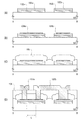
図1(A)乃至(D)に、本発明の一態様のFETの作製工程断面図を、また、図2(A)および(B)に、本発明の一態様のFETの作製工程上面図を示す。図1(A)乃至(D)は図2(A)および(B)のA−Bにおける断面図である。
本実施の形態では、実施の形態1で示したものとは異なる構造を有するFETの例を説明する。図3(A)および図3(B)に示すFETは、基板101上に、ゲート電極として機能する配線102a、102bと、配線102aの上に設けられ、配線102aと略同形状でゲート絶縁膜として機能する絶縁膜103aと、配線102bの上に設けられ、配線102bと略同形状でゲート絶縁膜として機能する絶縁膜103bと、絶縁膜103aの上に設けられ、その外周が絶縁膜103aの外周よりも内側にある半導体層104aと、絶縁膜103bの上に設けられ、その外周が絶縁膜103bの外周よりも内側にある半導体層104bと、酸化物絶縁層105と、平坦化絶縁層106と、酸化物絶縁層105と平坦化絶縁層106に設けられた開口部を通して半導体層104aに接する配線107aと、酸化物絶縁層105と平坦化絶縁層106に設けられた開口部を通して半導体層104bに接する配線107bとを有する点で、図1(D)に示すFETと同じである。
本実施の形態では、実施の形態1および2とは異なる構造を有するFETと、それをアクティブマトリクス回路に用いた例を説明する。アクティブマトリクス回路は、図5(A)に示される単位回路をマトリクス状に配置したものであり、図5(A)の回路は液晶表示装置のように、階調を電圧で制御する表示装置に用いられる。なお、図5(A)の回路以外に、一部のエレクトロルミネッセンス表示装置のように、階調を電流で制御する表示装置に用いられるアクティブマトリクス回路もある。
本実施の形態では、FETの信頼性を高めることのできる作製方法について図7を用いて説明する。なお、本実施の形態で説明するFETの半導体層や配線を上方から見た様子は図2に示されるものと同様であり、図2の一点鎖線A−Bで示される部分の断面の模式図を図7に示す。また、主たる構造も他の実施の形態と同じなので、それらを参照すればよい。
本実施の形態では、実施の形態1乃至4に示したFETを用いた電子機器について説明する。これらのFETは、パーソナルコンピュータ、携帯通信機器、画像表示装置、映像再生装置、画像映像撮像装置、ゲーム機、電子書籍等の機器に用いることができる。
102a 配線
102b 配線
103a 絶縁膜
103b 絶縁膜
104a 半導体層
104b 半導体層
104c 半導体層
104d 半導体層
105 酸化物絶縁層
105a 酸化物絶縁層
105b 酸化物絶縁層
105c 酸化物絶縁層
105d 酸化物絶縁層
106 平坦化絶縁層
106a 第1の保護絶縁層
106b 第2の保護絶縁層
107a 配線
107b 配線
108 絶縁膜
108a 絶縁膜
108b 絶縁膜
201 基板
202a 配線
202b 配線
203 絶縁膜
204a 半導体層
204b 半導体層
205a 配線
205b 配線
206 平坦化絶縁層
207a 配線
207b 配線
301 FET
302 表示素子
303 保持容量
304 スキャン線
305 データ線
306 容量線
307 配線
308 配線の交差する部分
401 基板
402 絶縁膜
403 半導体層
404 酸化物絶縁層
405 平坦化絶縁層
406 絶縁膜
407 開口部
501 基板
502a 配線
502b 配線
503a 絶縁膜
503b 絶縁膜
504a 半導体層
504b 半導体層
505a 酸化物絶縁層
505b 酸化物絶縁層
506a 第1の保護絶縁層
506b 第2の保護絶縁層
507a 配線
507b 配線
507c 配線
507d 配線
508 隔壁
509 発光材料層
510 透明導電膜
511 配線交差部
512 容量素子
Claims (9)
- 基板と、前記基板上に設けられた第1の配線と、前記第1の配線上に設けられ、前記第1の配線と略同形状の絶縁膜と、前記絶縁膜上に設けられた半導体層と、前記半導体層上に設けられた酸化物絶縁層と、前記酸化物絶縁層に設けられた開口部を通して、前記半導体層に接続する第2の配線とを有する電界効果トランジスタ。
- 前記半導体層が酸化物半導体よりなることを特徴とする請求項1記載の電界効果トランジスタ。
- 前記半導体層が、インジウムとガリウムを含むことを特徴とする請求項1または請求項2記載の電界効果トランジスタ。
- 前記酸化物絶縁層の厚さが、前記絶縁膜の厚さと前記半導体層の厚さの和の5倍以上である請求項1乃至3記載の電界効果トランジスタ。
- 前記酸化物絶縁層の厚さが、100nm以上である請求項1乃至3記載の電界効果トランジスタ。
- 前記半導体層の外周は、前記絶縁膜の外周の内側にあることを特徴とする請求項1乃至5記載の電界効果トランジスタ。
- 前記開口部は、前記半導体層と重なるように設けられることを特徴とする請求項1乃至6記載の電界効果トランジスタ。
- 基板上に第1の導電層を形成する工程と、
前記第1の導電層上に絶縁膜を形成する工程と、
前記絶縁膜を所定の形状に加工する工程と、
前記絶縁膜の形状と略同形状となるように前記第1の導電層を加工する工程と、
前記絶縁膜上に半導体層を形成する工程と、
前記半導体層上に酸化物絶縁層を形成する工程と
前記酸化物絶縁層に、前記半導体層に達する開口部を設ける工程と、
前記酸化物絶縁層を覆って第2の導電層を形成する工程と、を有することを特徴とする電界効果トランジスタの作製方法。 - 請求項8において、前記酸化物絶縁層を200℃以上で加熱する工程を有することを特徴とする電界効果トランジスタの作製方法。
Priority Applications (1)
| Application Number | Priority Date | Filing Date | Title |
|---|---|---|---|
| JP2011122996A JP5780836B2 (ja) | 2010-06-01 | 2011-06-01 | 電界効果トランジスタおよびその作製方法 |
Applications Claiming Priority (3)
| Application Number | Priority Date | Filing Date | Title |
|---|---|---|---|
| JP2010125443 | 2010-06-01 | ||
| JP2010125443 | 2010-06-01 | ||
| JP2011122996A JP5780836B2 (ja) | 2010-06-01 | 2011-06-01 | 電界効果トランジスタおよびその作製方法 |
Related Child Applications (1)
| Application Number | Title | Priority Date | Filing Date |
|---|---|---|---|
| JP2015140175A Division JP6091556B2 (ja) | 2010-06-01 | 2015-07-14 | 電子機器の作製方法 |
Publications (3)
| Publication Number | Publication Date |
|---|---|
| JP2012015496A true JP2012015496A (ja) | 2012-01-19 |
| JP2012015496A5 JP2012015496A5 (ja) | 2014-06-19 |
| JP5780836B2 JP5780836B2 (ja) | 2015-09-16 |
Family
ID=45021331
Family Applications (3)
| Application Number | Title | Priority Date | Filing Date |
|---|---|---|---|
| JP2011122996A Expired - Fee Related JP5780836B2 (ja) | 2010-06-01 | 2011-06-01 | 電界効果トランジスタおよびその作製方法 |
| JP2015140175A Expired - Fee Related JP6091556B2 (ja) | 2010-06-01 | 2015-07-14 | 電子機器の作製方法 |
| JP2016240541A Expired - Fee Related JP6250777B2 (ja) | 2010-06-01 | 2016-12-12 | 電子機器の作製方法 |
Family Applications After (2)
| Application Number | Title | Priority Date | Filing Date |
|---|---|---|---|
| JP2015140175A Expired - Fee Related JP6091556B2 (ja) | 2010-06-01 | 2015-07-14 | 電子機器の作製方法 |
| JP2016240541A Expired - Fee Related JP6250777B2 (ja) | 2010-06-01 | 2016-12-12 | 電子機器の作製方法 |
Country Status (2)
| Country | Link |
|---|---|
| US (2) | US8895375B2 (ja) |
| JP (3) | JP5780836B2 (ja) |
Cited By (7)
| Publication number | Priority date | Publication date | Assignee | Title |
|---|---|---|---|---|
| JP2014103390A (ja) * | 2012-10-24 | 2014-06-05 | Semiconductor Energy Lab Co Ltd | 半導体装置及びその作製方法 |
| JP2014192420A (ja) * | 2013-03-28 | 2014-10-06 | Japan Display Inc | 半導体装置及びその製造方法並びにそれを用いた表示装置 |
| JP2014199907A (ja) * | 2012-10-24 | 2014-10-23 | 株式会社半導体エネルギー研究所 | 半導体装置及びその作製方法 |
| JPWO2013190838A1 (ja) * | 2012-06-21 | 2016-02-08 | 株式会社Joled | Tft基板およびその製造方法並びに有機el表示装置およびその製造方法 |
| JP2016042577A (ja) * | 2014-08-18 | 2016-03-31 | 群創光電股▲ふん▼有限公司Innolux Corporation | 薄膜トランジスタ及び表示パネル |
| JP2017143280A (ja) * | 2012-09-13 | 2017-08-17 | 株式会社半導体エネルギー研究所 | 表示装置 |
| WO2019049632A1 (ja) * | 2017-09-05 | 2019-03-14 | 株式会社アルバック | 半導体装置の製造方法、および、半導体装置 |
Families Citing this family (5)
| Publication number | Priority date | Publication date | Assignee | Title |
|---|---|---|---|---|
| US20130265010A1 (en) * | 2012-04-06 | 2013-10-10 | Semiconductor Energy Laboratory Co., Ltd. | Protective circuit module and battery pack |
| JP6496132B2 (ja) | 2013-12-02 | 2019-04-03 | 株式会社半導体エネルギー研究所 | 半導体装置 |
| CN104752514B (zh) * | 2013-12-26 | 2018-05-25 | 昆山工研院新型平板显示技术中心有限公司 | 一种薄膜晶体管及其制备方法和应用 |
| JP7399857B2 (ja) | 2018-07-10 | 2023-12-18 | 株式会社半導体エネルギー研究所 | 二次電池の保護回路 |
| JP7679305B2 (ja) * | 2019-11-08 | 2025-05-19 | 株式会社半導体エネルギー研究所 | 半導体装置 |
Citations (5)
| Publication number | Priority date | Publication date | Assignee | Title |
|---|---|---|---|---|
| JPH10189994A (ja) * | 1996-12-27 | 1998-07-21 | Sony Corp | 半導体装置及びその製造方法 |
| JP2007258675A (ja) * | 2006-02-21 | 2007-10-04 | Idemitsu Kosan Co Ltd | Tft基板及び反射型tft基板並びにそれらの製造方法 |
| JP2008070876A (ja) * | 2006-09-11 | 2008-03-27 | Beijing Boe Optoelectronics Technology Co Ltd | Tft―lcdアレイ基板及びその製造方法 |
| JP2008175930A (ja) * | 2007-01-17 | 2008-07-31 | Hitachi Displays Ltd | 表示装置および表示装置の製造方法 |
| JP2010021520A (ja) * | 2008-07-08 | 2010-01-28 | Samsung Mobile Display Co Ltd | 薄膜トランジスタ及びその製造方法、ならびに薄膜トランジスタを備える平板表示装置 |
Family Cites Families (129)
| Publication number | Priority date | Publication date | Assignee | Title |
|---|---|---|---|---|
| JPS60198861A (ja) | 1984-03-23 | 1985-10-08 | Fujitsu Ltd | 薄膜トランジスタ |
| JPS61203484A (ja) | 1985-03-06 | 1986-09-09 | 株式会社東芝 | 表示装置用駆動回路基板及びその製造方法 |
| JPH0244256B2 (ja) | 1987-01-28 | 1990-10-03 | Kagaku Gijutsucho Mukizaishitsu Kenkyushocho | Ingazn2o5deshimesarerurotsuhoshokeinosojokozoojusurukagobutsuoyobisonoseizoho |
| JPH0244258B2 (ja) | 1987-02-24 | 1990-10-03 | Kagaku Gijutsucho Mukizaishitsu Kenkyushocho | Ingazn3o6deshimesarerurotsuhoshokeinosojokozoojusurukagobutsuoyobisonoseizoho |
| JPH0244260B2 (ja) | 1987-02-24 | 1990-10-03 | Kagaku Gijutsucho Mukizaishitsu Kenkyushocho | Ingazn5o8deshimesarerurotsuhoshokeinosojokozoojusurukagobutsuoyobisonoseizoho |
| JPS63210023A (ja) | 1987-02-24 | 1988-08-31 | Natl Inst For Res In Inorg Mater | InGaZn↓4O↓7で示される六方晶系の層状構造を有する化合物およびその製造法 |
| JPH0244262B2 (ja) | 1987-02-27 | 1990-10-03 | Kagaku Gijutsucho Mukizaishitsu Kenkyushocho | Ingazn6o9deshimesarerurotsuhoshokeinosojokozoojusurukagobutsuoyobisonoseizoho |
| JPH0244263B2 (ja) | 1987-04-22 | 1990-10-03 | Kagaku Gijutsucho Mukizaishitsu Kenkyushocho | Ingazn7o10deshimesarerurotsuhoshokeinosojokozoojusurukagobutsuoyobisonoseizoho |
| JP2715521B2 (ja) | 1989-02-15 | 1998-02-18 | カシオ計算機株式会社 | 薄膜トランジスタの製造方法 |
| US5087584A (en) * | 1990-04-30 | 1992-02-11 | Intel Corporation | Process for fabricating a contactless floating gate memory array utilizing wordline trench vias |
| JPH05251705A (ja) | 1992-03-04 | 1993-09-28 | Fuji Xerox Co Ltd | 薄膜トランジスタ |
| JP3479375B2 (ja) | 1995-03-27 | 2003-12-15 | 科学技術振興事業団 | 亜酸化銅等の金属酸化物半導体による薄膜トランジスタとpn接合を形成した金属酸化物半導体装置およびそれらの製造方法 |
| WO1997006554A2 (en) | 1995-08-03 | 1997-02-20 | Philips Electronics N.V. | Semiconductor device provided with transparent switching element |
| JP3625598B2 (ja) | 1995-12-30 | 2005-03-02 | 三星電子株式会社 | 液晶表示装置の製造方法 |
| CN1169015C (zh) | 1996-05-15 | 2004-09-29 | 精工爱普生株式会社 | 具有涂敷膜的薄膜器件、液晶屏以及薄膜器件的制造方法 |
| JPH10275913A (ja) * | 1997-03-28 | 1998-10-13 | Sanyo Electric Co Ltd | 半導体装置、半導体装置の製造方法及び薄膜トランジスタの製造方法 |
| JP4170454B2 (ja) | 1998-07-24 | 2008-10-22 | Hoya株式会社 | 透明導電性酸化物薄膜を有する物品及びその製造方法 |
| JP4386978B2 (ja) * | 1998-08-07 | 2009-12-16 | 株式会社半導体エネルギー研究所 | 半導体装置の作製方法 |
| JP2000150861A (ja) | 1998-11-16 | 2000-05-30 | Tdk Corp | 酸化物薄膜 |
| JP3276930B2 (ja) | 1998-11-17 | 2002-04-22 | 科学技術振興事業団 | トランジスタ及び半導体装置 |
| TW460731B (en) | 1999-09-03 | 2001-10-21 | Ind Tech Res Inst | Electrode structure and production method of wide viewing angle LCD |
| JP2001311965A (ja) | 2000-04-28 | 2001-11-09 | Nec Corp | アクティブマトリクス基板及びその製造方法 |
| JP4089858B2 (ja) | 2000-09-01 | 2008-05-28 | 国立大学法人東北大学 | 半導体デバイス |
| KR20020038482A (ko) | 2000-11-15 | 2002-05-23 | 모리시타 요이찌 | 박막 트랜지스터 어레이, 그 제조방법 및 그것을 이용한표시패널 |
| KR100704510B1 (ko) * | 2001-02-12 | 2007-04-09 | 엘지.필립스 엘시디 주식회사 | 횡전계형 액정표시장치용 하부 기판 및 그의 제조방법 |
| JP3997731B2 (ja) | 2001-03-19 | 2007-10-24 | 富士ゼロックス株式会社 | 基材上に結晶性半導体薄膜を形成する方法 |
| JP2002289859A (ja) | 2001-03-23 | 2002-10-04 | Minolta Co Ltd | 薄膜トランジスタ |
| JP3925839B2 (ja) | 2001-09-10 | 2007-06-06 | シャープ株式会社 | 半導体記憶装置およびその試験方法 |
| JP4090716B2 (ja) | 2001-09-10 | 2008-05-28 | 雅司 川崎 | 薄膜トランジスタおよびマトリクス表示装置 |
| JP4164562B2 (ja) | 2002-09-11 | 2008-10-15 | 独立行政法人科学技術振興機構 | ホモロガス薄膜を活性層として用いる透明薄膜電界効果型トランジスタ |
| EP1443130B1 (en) | 2001-11-05 | 2011-09-28 | Japan Science and Technology Agency | Natural superlattice homologous single crystal thin film, method for preparation thereof, and device using said single crystal thin film |
| JP4083486B2 (ja) | 2002-02-21 | 2008-04-30 | 独立行政法人科学技術振興機構 | LnCuO(S,Se,Te)単結晶薄膜の製造方法 |
| CN1445821A (zh) | 2002-03-15 | 2003-10-01 | 三洋电机株式会社 | ZnO膜和ZnO半导体层的形成方法、半导体元件及其制造方法 |
| JP3933591B2 (ja) | 2002-03-26 | 2007-06-20 | 淳二 城戸 | 有機エレクトロルミネッセント素子 |
| US7339187B2 (en) | 2002-05-21 | 2008-03-04 | State Of Oregon Acting By And Through The Oregon State Board Of Higher Education On Behalf Of Oregon State University | Transistor structures |
| JP2004022625A (ja) | 2002-06-13 | 2004-01-22 | Murata Mfg Co Ltd | 半導体デバイス及び該半導体デバイスの製造方法 |
| US7105868B2 (en) | 2002-06-24 | 2006-09-12 | Cermet, Inc. | High-electron mobility transistor with zinc oxide |
| US7067843B2 (en) | 2002-10-11 | 2006-06-27 | E. I. Du Pont De Nemours And Company | Transparent oxide semiconductor thin film transistors |
| JP4166105B2 (ja) | 2003-03-06 | 2008-10-15 | シャープ株式会社 | 半導体装置およびその製造方法 |
| JP2004273732A (ja) | 2003-03-07 | 2004-09-30 | Sharp Corp | アクティブマトリクス基板およびその製造方法 |
| JP4108633B2 (ja) | 2003-06-20 | 2008-06-25 | シャープ株式会社 | 薄膜トランジスタおよびその製造方法ならびに電子デバイス |
| US7262463B2 (en) | 2003-07-25 | 2007-08-28 | Hewlett-Packard Development Company, L.P. | Transistor including a deposited channel region having a doped portion |
| US7297977B2 (en) | 2004-03-12 | 2007-11-20 | Hewlett-Packard Development Company, L.P. | Semiconductor device |
| US7145174B2 (en) | 2004-03-12 | 2006-12-05 | Hewlett-Packard Development Company, Lp. | Semiconductor device |
| EP2413366B1 (en) | 2004-03-12 | 2017-01-11 | Japan Science And Technology Agency | A switching element of LCDs or organic EL displays |
| US7282782B2 (en) | 2004-03-12 | 2007-10-16 | Hewlett-Packard Development Company, L.P. | Combined binary oxide semiconductor device |
| US7211825B2 (en) | 2004-06-14 | 2007-05-01 | Yi-Chi Shih | Indium oxide-based thin film transistors and circuits |
| JP2006100760A (ja) | 2004-09-02 | 2006-04-13 | Casio Comput Co Ltd | 薄膜トランジスタおよびその製造方法 |
| US7285501B2 (en) | 2004-09-17 | 2007-10-23 | Hewlett-Packard Development Company, L.P. | Method of forming a solution processed device |
| US7298084B2 (en) | 2004-11-02 | 2007-11-20 | 3M Innovative Properties Company | Methods and displays utilizing integrated zinc oxide row and column drivers in conjunction with organic light emitting diodes |
| RU2369940C2 (ru) | 2004-11-10 | 2009-10-10 | Кэнон Кабусики Кайся | Аморфный оксид и полевой транзистор с его использованием |
| US7863611B2 (en) | 2004-11-10 | 2011-01-04 | Canon Kabushiki Kaisha | Integrated circuits utilizing amorphous oxides |
| US7829444B2 (en) | 2004-11-10 | 2010-11-09 | Canon Kabushiki Kaisha | Field effect transistor manufacturing method |
| CA2585063C (en) | 2004-11-10 | 2013-01-15 | Canon Kabushiki Kaisha | Light-emitting device |
| US7453065B2 (en) | 2004-11-10 | 2008-11-18 | Canon Kabushiki Kaisha | Sensor and image pickup device |
| EP1815530B1 (en) | 2004-11-10 | 2021-02-17 | Canon Kabushiki Kaisha | Field effect transistor employing an amorphous oxide |
| US7791072B2 (en) | 2004-11-10 | 2010-09-07 | Canon Kabushiki Kaisha | Display |
| US7579224B2 (en) | 2005-01-21 | 2009-08-25 | Semiconductor Energy Laboratory Co., Ltd. | Method for manufacturing a thin film semiconductor device |
| TWI390735B (zh) | 2005-01-28 | 2013-03-21 | 半導體能源研究所股份有限公司 | 半導體裝置,電子裝置,和半導體裝置的製造方法 |
| TWI505473B (zh) | 2005-01-28 | 2015-10-21 | 半導體能源研究所股份有限公司 | 半導體裝置,電子裝置,和半導體裝置的製造方法 |
| US7858451B2 (en) | 2005-02-03 | 2010-12-28 | Semiconductor Energy Laboratory Co., Ltd. | Electronic device, semiconductor device and manufacturing method thereof |
| US7948171B2 (en) | 2005-02-18 | 2011-05-24 | Semiconductor Energy Laboratory Co., Ltd. | Light emitting device |
| US20060197092A1 (en) | 2005-03-03 | 2006-09-07 | Randy Hoffman | System and method for forming conductive material on a substrate |
| US8681077B2 (en) | 2005-03-18 | 2014-03-25 | Semiconductor Energy Laboratory Co., Ltd. | Semiconductor device, and display device, driving method and electronic apparatus thereof |
| WO2006105077A2 (en) | 2005-03-28 | 2006-10-05 | Massachusetts Institute Of Technology | Low voltage thin film transistor with high-k dielectric material |
| US7645478B2 (en) | 2005-03-31 | 2010-01-12 | 3M Innovative Properties Company | Methods of making displays |
| US8300031B2 (en) | 2005-04-20 | 2012-10-30 | Semiconductor Energy Laboratory Co., Ltd. | Semiconductor device comprising transistor having gate and drain connected through a current-voltage conversion element |
| JP2006344849A (ja) | 2005-06-10 | 2006-12-21 | Casio Comput Co Ltd | 薄膜トランジスタ |
| US7402506B2 (en) | 2005-06-16 | 2008-07-22 | Eastman Kodak Company | Methods of making thin film transistors comprising zinc-oxide-based semiconductor materials and transistors made thereby |
| US7691666B2 (en) | 2005-06-16 | 2010-04-06 | Eastman Kodak Company | Methods of making thin film transistors comprising zinc-oxide-based semiconductor materials and transistors made thereby |
| US7507618B2 (en) | 2005-06-27 | 2009-03-24 | 3M Innovative Properties Company | Method for making electronic devices using metal oxide nanoparticles |
| KR100711890B1 (ko) | 2005-07-28 | 2007-04-25 | 삼성에스디아이 주식회사 | 유기 발광표시장치 및 그의 제조방법 |
| JP2007059128A (ja) | 2005-08-23 | 2007-03-08 | Canon Inc | 有機el表示装置およびその製造方法 |
| JP4280736B2 (ja) | 2005-09-06 | 2009-06-17 | キヤノン株式会社 | 半導体素子 |
| JP4850457B2 (ja) | 2005-09-06 | 2012-01-11 | キヤノン株式会社 | 薄膜トランジスタ及び薄膜ダイオード |
| JP2007073705A (ja) | 2005-09-06 | 2007-03-22 | Canon Inc | 酸化物半導体チャネル薄膜トランジスタおよびその製造方法 |
| JP5116225B2 (ja) | 2005-09-06 | 2013-01-09 | キヤノン株式会社 | 酸化物半導体デバイスの製造方法 |
| EP3614442A3 (en) | 2005-09-29 | 2020-03-25 | Semiconductor Energy Laboratory Co., Ltd. | Semiconductor device having oxide semiconductor layer and manufactoring method thereof |
| JP5037808B2 (ja) | 2005-10-20 | 2012-10-03 | キヤノン株式会社 | アモルファス酸化物を用いた電界効果型トランジスタ、及び該トランジスタを用いた表示装置 |
| CN101283444B (zh) | 2005-11-15 | 2011-01-26 | 株式会社半导体能源研究所 | 半导体器件及其制造方法 |
| KR101213871B1 (ko) * | 2005-12-15 | 2012-12-18 | 엘지디스플레이 주식회사 | 박막 트랜지스터 어레이 기판 및 그 제조 방법 |
| TWI292281B (en) | 2005-12-29 | 2008-01-01 | Ind Tech Res Inst | Pixel structure of active organic light emitting diode and method of fabricating the same |
| US7867636B2 (en) | 2006-01-11 | 2011-01-11 | Murata Manufacturing Co., Ltd. | Transparent conductive film and method for manufacturing the same |
| JP4977478B2 (ja) | 2006-01-21 | 2012-07-18 | 三星電子株式会社 | ZnOフィルム及びこれを用いたTFTの製造方法 |
| US20090001374A1 (en) | 2006-01-31 | 2009-01-01 | Kazuyoshi Inoue | Tft Substrate, Reflective Tft Substrate and Method for Manufacturing These Substrates |
| US7576394B2 (en) | 2006-02-02 | 2009-08-18 | Kochi Industrial Promotion Center | Thin film transistor including low resistance conductive thin films and manufacturing method thereof |
| US7977169B2 (en) | 2006-02-15 | 2011-07-12 | Kochi Industrial Promotion Center | Semiconductor device including active layer made of zinc oxide with controlled orientations and manufacturing method thereof |
| KR20070101595A (ko) | 2006-04-11 | 2007-10-17 | 삼성전자주식회사 | ZnO TFT |
| US20070252928A1 (en) | 2006-04-28 | 2007-11-01 | Toppan Printing Co., Ltd. | Structure, transmission type liquid crystal display, reflection type display and manufacturing method thereof |
| TWI275184B (en) | 2006-05-18 | 2007-03-01 | Au Optronics Corp | Thin film transistor and fabrication method thereof |
| JP5028033B2 (ja) | 2006-06-13 | 2012-09-19 | キヤノン株式会社 | 酸化物半導体膜のドライエッチング方法 |
| JP4999400B2 (ja) | 2006-08-09 | 2012-08-15 | キヤノン株式会社 | 酸化物半導体膜のドライエッチング方法 |
| JP4609797B2 (ja) | 2006-08-09 | 2011-01-12 | Nec液晶テクノロジー株式会社 | 薄膜デバイス及びその製造方法 |
| JP5128792B2 (ja) * | 2006-08-31 | 2013-01-23 | 財団法人高知県産業振興センター | 薄膜トランジスタの製法 |
| JP4332545B2 (ja) | 2006-09-15 | 2009-09-16 | キヤノン株式会社 | 電界効果型トランジスタ及びその製造方法 |
| JP4274219B2 (ja) | 2006-09-27 | 2009-06-03 | セイコーエプソン株式会社 | 電子デバイス、有機エレクトロルミネッセンス装置、有機薄膜半導体装置 |
| JP5164357B2 (ja) | 2006-09-27 | 2013-03-21 | キヤノン株式会社 | 半導体装置及び半導体装置の製造方法 |
| US7622371B2 (en) | 2006-10-10 | 2009-11-24 | Hewlett-Packard Development Company, L.P. | Fused nanocrystal thin film semiconductor and method |
| US7772021B2 (en) | 2006-11-29 | 2010-08-10 | Samsung Electronics Co., Ltd. | Flat panel displays comprising a thin-film transistor having a semiconductive oxide in its channel and methods of fabricating the same for use in flat panel displays |
| JP2008140684A (ja) | 2006-12-04 | 2008-06-19 | Toppan Printing Co Ltd | カラーelディスプレイおよびその製造方法 |
| JP5305630B2 (ja) * | 2006-12-05 | 2013-10-02 | キヤノン株式会社 | ボトムゲート型薄膜トランジスタの製造方法及び表示装置の製造方法 |
| KR101303578B1 (ko) | 2007-01-05 | 2013-09-09 | 삼성전자주식회사 | 박막 식각 방법 |
| US8207063B2 (en) | 2007-01-26 | 2012-06-26 | Eastman Kodak Company | Process for atomic layer deposition |
| KR100851215B1 (ko) | 2007-03-14 | 2008-08-07 | 삼성에스디아이 주식회사 | 박막 트랜지스터 및 이를 이용한 유기 전계 발광표시장치 |
| US7795613B2 (en) | 2007-04-17 | 2010-09-14 | Toppan Printing Co., Ltd. | Structure with transistor |
| KR101325053B1 (ko) | 2007-04-18 | 2013-11-05 | 삼성디스플레이 주식회사 | 박막 트랜지스터 기판 및 이의 제조 방법 |
| KR20080094300A (ko) | 2007-04-19 | 2008-10-23 | 삼성전자주식회사 | 박막 트랜지스터 및 그 제조 방법과 박막 트랜지스터를포함하는 평판 디스플레이 |
| KR101334181B1 (ko) | 2007-04-20 | 2013-11-28 | 삼성전자주식회사 | 선택적으로 결정화된 채널층을 갖는 박막 트랜지스터 및 그제조 방법 |
| WO2008133345A1 (en) | 2007-04-25 | 2008-11-06 | Canon Kabushiki Kaisha | Oxynitride semiconductor |
| KR101334182B1 (ko) * | 2007-05-28 | 2013-11-28 | 삼성전자주식회사 | ZnO 계 박막 트랜지스터의 제조방법 |
| KR101345376B1 (ko) | 2007-05-29 | 2013-12-24 | 삼성전자주식회사 | ZnO 계 박막 트랜지스터 및 그 제조방법 |
| US8202365B2 (en) | 2007-12-17 | 2012-06-19 | Fujifilm Corporation | Process for producing oriented inorganic crystalline film, and semiconductor device using the oriented inorganic crystalline film |
| JP5467728B2 (ja) | 2008-03-14 | 2014-04-09 | 富士フイルム株式会社 | 薄膜電界効果型トランジスタおよびその製造方法 |
| JP2010016072A (ja) | 2008-07-02 | 2010-01-21 | Canon Inc | 薄膜トランジスタ |
| JP5584960B2 (ja) * | 2008-07-03 | 2014-09-10 | ソニー株式会社 | 薄膜トランジスタおよび表示装置 |
| JP5330779B2 (ja) * | 2008-09-10 | 2013-10-30 | 三菱電機株式会社 | 光電変換装置、及びその製造方法 |
| JP4623179B2 (ja) | 2008-09-18 | 2011-02-02 | ソニー株式会社 | 薄膜トランジスタおよびその製造方法 |
| KR101827333B1 (ko) | 2008-09-19 | 2018-02-09 | 가부시키가이샤 한도오따이 에네루기 켄큐쇼 | 반도체장치 |
| JP5451280B2 (ja) | 2008-10-09 | 2014-03-26 | キヤノン株式会社 | ウルツ鉱型結晶成長用基板およびその製造方法ならびに半導体装置 |
| KR20170021903A (ko) | 2008-11-07 | 2017-02-28 | 가부시키가이샤 한도오따이 에네루기 켄큐쇼 | 반도체 장치의 제작 방법 |
| KR101019048B1 (ko) | 2008-11-20 | 2011-03-07 | 엘지디스플레이 주식회사 | 어레이 기판 및 이의 제조방법 |
| EP2256814B1 (en) | 2009-05-29 | 2019-01-16 | Semiconductor Energy Laboratory Co, Ltd. | Oxide semiconductor device and method for manufacturing the same |
| WO2011001881A1 (en) | 2009-06-30 | 2011-01-06 | Semiconductor Energy Laboratory Co., Ltd. | Method for manufacturing semiconductor device |
| KR102153841B1 (ko) | 2009-07-31 | 2020-09-08 | 가부시키가이샤 한도오따이 에네루기 켄큐쇼 | 반도체 장치 및 그 제조 방법 |
| WO2011013522A1 (en) | 2009-07-31 | 2011-02-03 | Semiconductor Energy Laboratory Co., Ltd. | Semiconductor device and manufacturing method thereof |
| KR101913995B1 (ko) | 2009-07-31 | 2018-10-31 | 가부시키가이샤 한도오따이 에네루기 켄큐쇼 | 반도체 장치 및 그 제작 방법 |
| WO2011013523A1 (en) | 2009-07-31 | 2011-02-03 | Semiconductor Energy Laboratory Co., Ltd. | Semiconductor device and method for manufacturing the same |
| CN102576677B (zh) | 2009-09-24 | 2015-07-22 | 株式会社半导体能源研究所 | 半导体元件及其制造方法 |
| KR20120102653A (ko) | 2009-10-30 | 2012-09-18 | 가부시키가이샤 한도오따이 에네루기 켄큐쇼 | 반도체 장치 및 반도체 장치의 제작방법 |
-
2011
- 2011-05-24 US US13/114,634 patent/US8895375B2/en not_active Expired - Fee Related
- 2011-06-01 JP JP2011122996A patent/JP5780836B2/ja not_active Expired - Fee Related
-
2014
- 2014-11-17 US US14/542,705 patent/US9812560B2/en not_active Expired - Fee Related
-
2015
- 2015-07-14 JP JP2015140175A patent/JP6091556B2/ja not_active Expired - Fee Related
-
2016
- 2016-12-12 JP JP2016240541A patent/JP6250777B2/ja not_active Expired - Fee Related
Patent Citations (5)
| Publication number | Priority date | Publication date | Assignee | Title |
|---|---|---|---|---|
| JPH10189994A (ja) * | 1996-12-27 | 1998-07-21 | Sony Corp | 半導体装置及びその製造方法 |
| JP2007258675A (ja) * | 2006-02-21 | 2007-10-04 | Idemitsu Kosan Co Ltd | Tft基板及び反射型tft基板並びにそれらの製造方法 |
| JP2008070876A (ja) * | 2006-09-11 | 2008-03-27 | Beijing Boe Optoelectronics Technology Co Ltd | Tft―lcdアレイ基板及びその製造方法 |
| JP2008175930A (ja) * | 2007-01-17 | 2008-07-31 | Hitachi Displays Ltd | 表示装置および表示装置の製造方法 |
| JP2010021520A (ja) * | 2008-07-08 | 2010-01-28 | Samsung Mobile Display Co Ltd | 薄膜トランジスタ及びその製造方法、ならびに薄膜トランジスタを備える平板表示装置 |
Cited By (24)
| Publication number | Priority date | Publication date | Assignee | Title |
|---|---|---|---|---|
| JPWO2013190838A1 (ja) * | 2012-06-21 | 2016-02-08 | 株式会社Joled | Tft基板およびその製造方法並びに有機el表示装置およびその製造方法 |
| US10446584B2 (en) | 2012-09-13 | 2019-10-15 | Semiconductor Energy Laboratory Co., Ltd. | Semiconductor device |
| US10236305B2 (en) | 2012-09-13 | 2019-03-19 | Semiconductor Energy Laboratory Co., Ltd. | Semiconductor device |
| US12080717B2 (en) | 2012-09-13 | 2024-09-03 | Semiconductor Energy Laboratory Co., Ltd. | Semiconductor device |
| US10700099B2 (en) | 2012-09-13 | 2020-06-30 | Semiconductor Energy Laboratory Co., Ltd. | Semiconductor device |
| JP2017143280A (ja) * | 2012-09-13 | 2017-08-17 | 株式会社半導体エネルギー研究所 | 表示装置 |
| US9806099B2 (en) | 2012-09-13 | 2017-10-31 | Semiconductor Energy Laboratory Co., Ltd. | Semiconductor device |
| US9997639B2 (en) | 2012-10-24 | 2018-06-12 | Semiconductor Energy Laboratory Co., Ltd. | Semiconductor device and method for manufacturing the same |
| US10749015B2 (en) | 2012-10-24 | 2020-08-18 | Semiconductor Energy Laboratory Co., Ltd. | Semiconductor device and method for manufacturing the same |
| JP2014103390A (ja) * | 2012-10-24 | 2014-06-05 | Semiconductor Energy Lab Co Ltd | 半導体装置及びその作製方法 |
| US12495619B2 (en) | 2012-10-24 | 2025-12-09 | Semiconductor Energy Laboratory Co., Ltd. | Semiconductor device and method for manufacturing the same |
| JP2014199907A (ja) * | 2012-10-24 | 2014-10-23 | 株式会社半導体エネルギー研究所 | 半導体装置及びその作製方法 |
| US10361291B2 (en) | 2012-10-24 | 2019-07-23 | Semiconductor Energy Laboratory Co., Ltd. | Semiconductor device and method for manufacturing the same |
| US11824105B2 (en) | 2012-10-24 | 2023-11-21 | Semiconductor Energy Laboratory Co., Ltd. | Semiconductor device and method for manufacturing the same |
| US10516062B2 (en) | 2012-10-24 | 2019-12-24 | Semiconductor Energy Laboratory Co., Ltd. | Semiconductor device and method for manufacturing the same |
| US11355648B2 (en) | 2012-10-24 | 2022-06-07 | Semiconductor Energy Laboratory Co., Ltd. | Semiconductor device and method for manufacturing the same |
| US11152494B2 (en) | 2012-10-24 | 2021-10-19 | Semiconductor Energy Laboratory Co., Ltd. | Semiconductor device and method for manufacturing the same |
| JP2014192420A (ja) * | 2013-03-28 | 2014-10-06 | Japan Display Inc | 半導体装置及びその製造方法並びにそれを用いた表示装置 |
| JP2016042577A (ja) * | 2014-08-18 | 2016-03-31 | 群創光電股▲ふん▼有限公司Innolux Corporation | 薄膜トランジスタ及び表示パネル |
| KR102229705B1 (ko) * | 2017-09-05 | 2021-03-18 | 가부시키가이샤 알박 | 반도체 장치를 제조하기 위한 방법 및 반도체 장치 |
| JPWO2019049632A1 (ja) * | 2017-09-05 | 2019-11-07 | 株式会社アルバック | 半導体装置の製造方法、および、半導体装置 |
| US11411120B2 (en) | 2017-09-05 | 2022-08-09 | Ulvac, Inc. | Method for manufacturing semiconductor device using plasma CVD process |
| WO2019049632A1 (ja) * | 2017-09-05 | 2019-03-14 | 株式会社アルバック | 半導体装置の製造方法、および、半導体装置 |
| KR20190059979A (ko) * | 2017-09-05 | 2019-05-31 | 가부시키가이샤 알박 | 반도체 장치를 제조하기 위한 방법 및 반도체 장치 |
Also Published As
| Publication number | Publication date |
|---|---|
| JP6091556B2 (ja) | 2017-03-08 |
| US9812560B2 (en) | 2017-11-07 |
| US8895375B2 (en) | 2014-11-25 |
| JP6250777B2 (ja) | 2017-12-20 |
| US20110291092A1 (en) | 2011-12-01 |
| JP2017050572A (ja) | 2017-03-09 |
| JP5780836B2 (ja) | 2015-09-16 |
| JP2015195399A (ja) | 2015-11-05 |
| US20150072471A1 (en) | 2015-03-12 |
Similar Documents
| Publication | Publication Date | Title |
|---|---|---|
| JP5780836B2 (ja) | 電界効果トランジスタおよびその作製方法 | |
| JP7441282B2 (ja) | 半導体装置 | |
| JP6298139B2 (ja) | 電界効果トランジスタ | |
| US8053773B2 (en) | Thin film transistor, flat panel display device having the same, and associated methods | |
| TWI623101B (zh) | 半導體裝置及其製造方法 | |
| JP2025137548A (ja) | 半導体装置 | |
| EP3723130B1 (en) | Array substrate and manufacturing method therefor, and display apparatus | |
| JP6113500B2 (ja) | 半導体装置及び半導体装置の製造方法 | |
| JP6798942B2 (ja) | トランジスタおよび半導体装置 | |
| CN105849878A (zh) | 具有未图案化的蚀刻停止的motft | |
| WO2015140656A1 (en) | Semiconductor device and manufacturing method thereof | |
| TW202324608A (zh) | 主動元件基板、電容裝置以及主動元件基板的製造方法 | |
| US20170373194A1 (en) | Transistor | |
| KR102605008B1 (ko) | 반도체 장치, 전자 부품, 및 전자 기기 | |
| US20170373192A1 (en) | Transistor and semiconductor device | |
| EP3480853A1 (en) | Method for manufacturing thin-film transistor and thin-film transistor | |
| US11777502B2 (en) | Logic circuit and semiconductor device formed using unipolar transistor | |
| KR20210077716A (ko) | 단극성 레벨 시프트 회로 및 반도체 장치 | |
| US10971528B2 (en) | Semiconductor device | |
| JP7550948B2 (ja) | 金属酸化物膜 | |
| KR20260044957A (ko) | 전자 디바이스 안정성을 향상시키기 위한 금속 산화물 층 인터페이스들의 엔지니어링 | |
| CN116565026A (zh) | 薄膜晶体管及其制备方法 | |
| TWI865344B (zh) | 薄膜電晶體及其製造方法 | |
| US12205892B2 (en) | Semiconductor device | |
| WO2018002757A1 (ja) | トランジスタ |
Legal Events
| Date | Code | Title | Description |
|---|---|---|---|
| A521 | Request for written amendment filed |
Free format text: JAPANESE INTERMEDIATE CODE: A523 Effective date: 20140430 |
|
| A621 | Written request for application examination |
Free format text: JAPANESE INTERMEDIATE CODE: A621 Effective date: 20140430 |
|
| A977 | Report on retrieval |
Free format text: JAPANESE INTERMEDIATE CODE: A971007 Effective date: 20150309 |
|
| A131 | Notification of reasons for refusal |
Free format text: JAPANESE INTERMEDIATE CODE: A131 Effective date: 20150317 |
|
| A521 | Request for written amendment filed |
Free format text: JAPANESE INTERMEDIATE CODE: A523 Effective date: 20150326 |
|
| TRDD | Decision of grant or rejection written | ||
| A01 | Written decision to grant a patent or to grant a registration (utility model) |
Free format text: JAPANESE INTERMEDIATE CODE: A01 Effective date: 20150630 |
|
| A61 | First payment of annual fees (during grant procedure) |
Free format text: JAPANESE INTERMEDIATE CODE: A61 Effective date: 20150714 |
|
| R150 | Certificate of patent or registration of utility model |
Ref document number: 5780836 Country of ref document: JP Free format text: JAPANESE INTERMEDIATE CODE: R150 |
|
| R250 | Receipt of annual fees |
Free format text: JAPANESE INTERMEDIATE CODE: R250 |
|
| R250 | Receipt of annual fees |
Free format text: JAPANESE INTERMEDIATE CODE: R250 |
|
| R250 | Receipt of annual fees |
Free format text: JAPANESE INTERMEDIATE CODE: R250 |
|
| R250 | Receipt of annual fees |
Free format text: JAPANESE INTERMEDIATE CODE: R250 |
|
| R250 | Receipt of annual fees |
Free format text: JAPANESE INTERMEDIATE CODE: R250 |
|
| LAPS | Cancellation because of no payment of annual fees |