JP2013201424A - 半導体装置の製造方法 - Google Patents
半導体装置の製造方法 Download PDFInfo
- Publication number
- JP2013201424A JP2013201424A JP2013022391A JP2013022391A JP2013201424A JP 2013201424 A JP2013201424 A JP 2013201424A JP 2013022391 A JP2013022391 A JP 2013022391A JP 2013022391 A JP2013022391 A JP 2013022391A JP 2013201424 A JP2013201424 A JP 2013201424A
- Authority
- JP
- Japan
- Prior art keywords
- substrate
- back surface
- treatment
- semiconductor device
- polishing
- Prior art date
- Legal status (The legal status is an assumption and is not a legal conclusion. Google has not performed a legal analysis and makes no representation as to the accuracy of the status listed.)
- Granted
Links
Images


Classifications
-
- H—ELECTRICITY
- H10—SEMICONDUCTOR DEVICES; ELECTRIC SOLID-STATE DEVICES NOT OTHERWISE PROVIDED FOR
- H10P—GENERIC PROCESSES OR APPARATUS FOR THE MANUFACTURE OR TREATMENT OF DEVICES COVERED BY CLASS H10
- H10P70/00—Cleaning of wafers, substrates or parts of devices
- H10P70/20—Cleaning during device manufacture
-
- B—PERFORMING OPERATIONS; TRANSPORTING
- B24—GRINDING; POLISHING
- B24B—MACHINES, DEVICES, OR PROCESSES FOR GRINDING OR POLISHING; DRESSING OR CONDITIONING OF ABRADING SURFACES; FEEDING OF GRINDING, POLISHING, OR LAPPING AGENTS
- B24B37/00—Lapping machines or devices; Accessories
- B24B37/04—Lapping machines or devices; Accessories designed for working plane surfaces
- B24B37/042—Lapping machines or devices; Accessories designed for working plane surfaces operating processes therefor
-
- B—PERFORMING OPERATIONS; TRANSPORTING
- B82—NANOTECHNOLOGY
- B82Y—SPECIFIC USES OR APPLICATIONS OF NANOSTRUCTURES; MEASUREMENT OR ANALYSIS OF NANOSTRUCTURES; MANUFACTURE OR TREATMENT OF NANOSTRUCTURES
- B82Y10/00—Nanotechnology for information processing, storage or transmission, e.g. quantum computing or single electron logic
-
- B—PERFORMING OPERATIONS; TRANSPORTING
- B82—NANOTECHNOLOGY
- B82Y—SPECIFIC USES OR APPLICATIONS OF NANOSTRUCTURES; MEASUREMENT OR ANALYSIS OF NANOSTRUCTURES; MANUFACTURE OR TREATMENT OF NANOSTRUCTURES
- B82Y40/00—Manufacture or treatment of nanostructures
-
- G—PHYSICS
- G03—PHOTOGRAPHY; CINEMATOGRAPHY; ANALOGOUS TECHNIQUES USING WAVES OTHER THAN OPTICAL WAVES; ELECTROGRAPHY; HOLOGRAPHY
- G03F—PHOTOMECHANICAL PRODUCTION OF TEXTURED OR PATTERNED SURFACES, e.g. FOR PRINTING, FOR PROCESSING OF SEMICONDUCTOR DEVICES; MATERIALS THEREFOR; ORIGINALS THEREFOR; APPARATUS SPECIALLY ADAPTED THEREFOR
- G03F7/00—Photomechanical, e.g. photolithographic, production of textured or patterned surfaces, e.g. printing surfaces; Materials therefor, e.g. comprising photoresists; Apparatus specially adapted therefor
- G03F7/004—Photosensitive materials
- G03F7/09—Photosensitive materials characterised by structural details, e.g. supports, auxiliary layers
- G03F7/092—Photosensitive materials characterised by structural details, e.g. supports, auxiliary layers characterised by backside coating or layers, by lubricating-slip layers or means, by oxygen barrier layers or by stripping-release layers or means
-
- H—ELECTRICITY
- H10—SEMICONDUCTOR DEVICES; ELECTRIC SOLID-STATE DEVICES NOT OTHERWISE PROVIDED FOR
- H10P—GENERIC PROCESSES OR APPARATUS FOR THE MANUFACTURE OR TREATMENT OF DEVICES COVERED BY CLASS H10
- H10P70/00—Cleaning of wafers, substrates or parts of devices
- H10P70/50—Cleaning of wafers, substrates or parts of devices characterised by the part to be cleaned
- H10P70/56—Cleaning of wafer backside
-
- H—ELECTRICITY
- H10—SEMICONDUCTOR DEVICES; ELECTRIC SOLID-STATE DEVICES NOT OTHERWISE PROVIDED FOR
- H10P—GENERIC PROCESSES OR APPARATUS FOR THE MANUFACTURE OR TREATMENT OF DEVICES COVERED BY CLASS H10
- H10P72/00—Handling or holding of wafers, substrates or devices during manufacture or treatment thereof
- H10P72/04—Apparatus for manufacture or treatment
- H10P72/0402—Apparatus for fluid treatment
- H10P72/0406—Apparatus for fluid treatment for cleaning followed by drying, rinsing, stripping, blasting or the like
- H10P72/0411—Apparatus for fluid treatment for cleaning followed by drying, rinsing, stripping, blasting or the like for wet cleaning or washing
- H10P72/0414—Apparatus for fluid treatment for cleaning followed by drying, rinsing, stripping, blasting or the like for wet cleaning or washing using mainly spraying means, e.g. nozzles
-
- H—ELECTRICITY
- H10—SEMICONDUCTOR DEVICES; ELECTRIC SOLID-STATE DEVICES NOT OTHERWISE PROVIDED FOR
- H10P—GENERIC PROCESSES OR APPARATUS FOR THE MANUFACTURE OR TREATMENT OF DEVICES COVERED BY CLASS H10
- H10P76/00—Manufacture or treatment of masks on semiconductor bodies, e.g. by lithography or photolithography
- H10P76/20—Manufacture or treatment of masks on semiconductor bodies, e.g. by lithography or photolithography of masks comprising organic materials
- H10P76/204—Manufacture or treatment of masks on semiconductor bodies, e.g. by lithography or photolithography of masks comprising organic materials of organic photoresist masks
- H10P76/2041—Photolithographic processes
-
- G—PHYSICS
- G03—PHOTOGRAPHY; CINEMATOGRAPHY; ANALOGOUS TECHNIQUES USING WAVES OTHER THAN OPTICAL WAVES; ELECTROGRAPHY; HOLOGRAPHY
- G03F—PHOTOMECHANICAL PRODUCTION OF TEXTURED OR PATTERNED SURFACES, e.g. FOR PRINTING, FOR PROCESSING OF SEMICONDUCTOR DEVICES; MATERIALS THEREFOR; ORIGINALS THEREFOR; APPARATUS SPECIALLY ADAPTED THEREFOR
- G03F7/00—Photomechanical, e.g. photolithographic, production of textured or patterned surfaces, e.g. printing surfaces; Materials therefor, e.g. comprising photoresists; Apparatus specially adapted therefor
- G03F7/0002—Lithographic processes using patterning methods other than those involving the exposure to radiation, e.g. by stamping
Landscapes
- Engineering & Computer Science (AREA)
- Chemical & Material Sciences (AREA)
- Nanotechnology (AREA)
- Physics & Mathematics (AREA)
- Crystallography & Structural Chemistry (AREA)
- General Physics & Mathematics (AREA)
- Condensed Matter Physics & Semiconductors (AREA)
- Manufacturing & Machinery (AREA)
- Structural Engineering (AREA)
- Architecture (AREA)
- Mechanical Engineering (AREA)
- Mathematical Physics (AREA)
- Theoretical Computer Science (AREA)
- Cleaning Or Drying Semiconductors (AREA)
- Mechanical Treatment Of Semiconductor (AREA)
- Exposure Of Semiconductors, Excluding Electron Or Ion Beam Exposure (AREA)
- Finish Polishing, Edge Sharpening, And Grinding By Specific Grinding Devices (AREA)
Abstract
【解決手段】半導体装置の製造方法であって、基板10の表面側を該表面と非接触に保持した状態で、基板10の裏面の傷又は異物を除去するための裏面処理を行う工程と(S2)、裏面処理が施された基板10の裏面をステージ上に接触させて保持し、基板10の表面にリソグラフィでパターン形成を行う工程と(S6)、を含む。
【選択図】 図1
Description
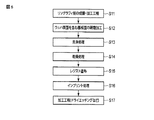
図1は、第1の実施形態に係る半導体装置の製造工程を説明するためのフローチャートである。ここでは、マスクを用いた光リソグラフィにより基板上にパターンを形成するものとする。
図5は、第2の実施形態に係る半導体装置の製造工程を説明するためのフローチャートである。ここでは、スタンパを用いたナノインプリント・リソグラフィ(NIL)により被処理基板上にパターンを形成するものとする。
図7は、第3の実施形態に係る半導体装置の製造工程を説明するためのフローチャートである。ステップS31,S33〜S38は第1の実施形態のステップS1,S3〜S8に対応している。
なお、本発明は上述した各実施形態に限定されるものではない。
11,61…Si基板
12,62…被加工膜
13,63…レジスト
20…静圧軸受け
21…導入管
22…ポケット
23…保持具
24…研磨ヘッド
25…ホルダー
26…処理部材
27…研磨液供給管
28…洗浄液供給管
30…ステージ
40…露光用マスク
41…石英ガラス
42…クロムパターン
45…レンズ系
48,64…異物
65…スタンパ
74…ノズル
75…供給管
76…ジェット流
Claims (14)
- 被処理基板の表面側を該表面と非接触に保持した状態で、前記基板の裏面の傷又は異物を除去するための裏面処理を行う工程と、
前記裏面処理が施された前記基板の裏面をステージ上に接触させて保持し、前記基板の表面にリソグラフィでパターン形成を行う工程と、
を含むことを特徴とする半導体装置の製造方法。 - 被処理基板の裏面側を該裏面と非接触に保持した状態で、前記基板の表面の傷又は異物を除去するための表面処理を行う工程と、
前記表面処理が施された前記基板の裏面をステージ上に接触させて保持し、前記基板の表面にインプリント・リソグラフィでパターン形成を行う工程と、
を含むことを特徴とする半導体装置の製造方法。 - 前記裏面処理又は前記表面処理を行う工程として、前記基板の裏面又は表面に、研磨部を接触させて摺動させる研磨処理を施すことを特徴とする、請求項1又は2に記載の半導体装置の製造方法。
- 前記研磨処理の際に、前記研磨部により前記基板に100hPa以上の押圧を加えることを特徴とする、請求項3記載の半導体装置の製造方法。
- 前記研磨処理の際に、前記基板よりも小径の研磨部を用い、該研磨部を基板面上で移動させることにより基板面の必要な部分を研磨することを特徴とする、請求項3又は4に記載の半導体装置の製造方法。
- 前記裏面処理又は前記表面処理を行う工程として、前記基板の裏面又は表面に、高圧気体と共に液体、固体、又はこれらの混合物をジェット流で噴射する処理を施すことを特徴とする、請求項1又は2に記載の半導体装置の製造方法。
- 前記ジェット流で噴射する際に、前記ジェット流を前記基板の裏面又は表面に対して斜め方向から照射することを特徴とする、請求項6記載の半導体装置の製造方法。
- 前記ジェット流で噴射する際に、前記高圧気体として不活性ガスを、前記液体として水を、及び前記固体として金属酸化物の粒子を用いたことを特徴とする、請求項6又は7に記載の半導体装置の製造方法。
- 前記基板の表面側又は裏面側を非接触で保持するために、前記基板の表面又は裏面に流体を供給する静圧軸受けを用いることを特徴とする、請求項1乃至8の何れか1項に記載の半導体装置の製造方法。
- 前記静圧軸受けのための流体は、前記基板の汚染要因にならない水、油、又は高圧空気であることを特徴とする、請求項9記載の半導体装置の製造方法。
- 前記裏面処理又は前記表面処理を行う工程の後で且つ前記パターン形成を行う工程の前に、前記基板の裏面又は表面を洗浄処理する工程と、続いて前記基板の裏面又は表面を乾燥処理する工程と、を更に含むことを特徴とする、請求項1乃至10の何れか1項に記載の半導体装置の製造方法。
- 前記裏面処理又は前記表面処理、前記洗浄処理、及び前記乾燥処理を、同一チャンバ内で行うことを特徴とする、請求項11記載の半導体装置の製造方法。
- 前記裏面処理又は前記表面処理を行う際及び前記洗浄処理を行う際は、前記基板の表面又は裏面に流体を供給する静圧軸受けを用いて前記基板を保持し、前記乾燥処理を行う際は、前記基板の側面に接触する保持具を用いて前記基板を保持することを特徴とする、請求項12記載の半導体装置の製造方法。
- 前記洗浄処理の際に、前記裏面処理又は前記表面処理による前記基板の処理面に、純水と共に薬液を供給することを特徴とする、請求項11乃至13の何れか1項に記載の半導体装置の製造方法。
Priority Applications (1)
| Application Number | Priority Date | Filing Date | Title |
|---|---|---|---|
| JP2013022391A JP6162417B2 (ja) | 2012-02-21 | 2013-02-07 | 半導体装置の製造方法 |
Applications Claiming Priority (3)
| Application Number | Priority Date | Filing Date | Title |
|---|---|---|---|
| JP2012035018 | 2012-02-21 | ||
| JP2012035018 | 2012-02-21 | ||
| JP2013022391A JP6162417B2 (ja) | 2012-02-21 | 2013-02-07 | 半導体装置の製造方法 |
Publications (2)
| Publication Number | Publication Date |
|---|---|
| JP2013201424A true JP2013201424A (ja) | 2013-10-03 |
| JP6162417B2 JP6162417B2 (ja) | 2017-07-12 |
Family
ID=48982594
Family Applications (1)
| Application Number | Title | Priority Date | Filing Date |
|---|---|---|---|
| JP2013022391A Expired - Fee Related JP6162417B2 (ja) | 2012-02-21 | 2013-02-07 | 半導体装置の製造方法 |
Country Status (2)
| Country | Link |
|---|---|
| US (2) | US20130217228A1 (ja) |
| JP (1) | JP6162417B2 (ja) |
Cited By (7)
| Publication number | Priority date | Publication date | Assignee | Title |
|---|---|---|---|---|
| JP2014220495A (ja) * | 2013-04-12 | 2014-11-20 | レーザーテック株式会社 | 異物除去装置 |
| JP2016198854A (ja) * | 2015-04-10 | 2016-12-01 | 株式会社東芝 | 処理装置 |
| KR20170037822A (ko) * | 2015-09-28 | 2017-04-05 | 도쿄엘렉트론가부시키가이샤 | 기판 처리 방법 및 기판 처리 장치 |
| KR20180061020A (ko) * | 2016-11-29 | 2018-06-07 | 도쿄엘렉트론가부시키가이샤 | 기판 처리 장치, 기판 처리 방법 및 기억 매체 |
| CN111261561A (zh) * | 2016-02-01 | 2020-06-09 | 株式会社斯库林集团 | 基板清洗装置及方法、基板处理装置及方法 |
| JP2020167438A (ja) * | 2016-02-01 | 2020-10-08 | 株式会社Screenホールディングス | 基板洗浄装置、基板処理装置、基板洗浄方法および基板処理方法 |
| WO2023074444A1 (ja) * | 2021-10-26 | 2023-05-04 | 株式会社Screenホールディングス | 基板処理方法および基板処理システム |
Families Citing this family (8)
| Publication number | Priority date | Publication date | Assignee | Title |
|---|---|---|---|---|
| JP6113960B2 (ja) * | 2012-02-21 | 2017-04-12 | 株式会社荏原製作所 | 基板処理装置および基板処理方法 |
| JP6920849B2 (ja) * | 2017-03-27 | 2021-08-18 | 株式会社荏原製作所 | 基板処理方法および装置 |
| JP7317532B2 (ja) * | 2019-03-19 | 2023-07-31 | キオクシア株式会社 | 研磨装置及び研磨方法 |
| JP2021044511A (ja) | 2019-09-13 | 2021-03-18 | キオクシア株式会社 | 半導体装置の製造方法 |
| JP7467188B2 (ja) | 2020-03-24 | 2024-04-15 | キオクシア株式会社 | Cmp方法及びcmp用洗浄剤 |
| JP7562453B2 (ja) | 2021-03-12 | 2024-10-07 | キオクシア株式会社 | 研磨液、研磨装置、及び研磨方法 |
| JP7746092B2 (ja) | 2021-09-24 | 2025-09-30 | 株式会社Screenホールディングス | 研磨装置、基板処理装置および研磨方法 |
| JP7660056B2 (ja) | 2021-11-17 | 2025-04-10 | 株式会社Screenホールディングス | 基板処理装置 |
Citations (9)
| Publication number | Priority date | Publication date | Assignee | Title |
|---|---|---|---|---|
| JPH0855826A (ja) * | 1994-08-10 | 1996-02-27 | Nec Corp | 研磨方法および研磨装置 |
| JPH0945684A (ja) * | 1995-07-28 | 1997-02-14 | Nec Corp | 半導体装置の製造方法およびその装置 |
| US5780204A (en) * | 1997-02-03 | 1998-07-14 | Advanced Micro Devices, Inc. | Backside wafer polishing for improved photolithography |
| JP2003297901A (ja) * | 2002-04-05 | 2003-10-17 | Supurauto:Kk | 基板処理システムおよびその処理方法 |
| JP2004223639A (ja) * | 2003-01-21 | 2004-08-12 | Femutekku:Kk | 薄膜構造物加工装置 |
| JP2006319249A (ja) * | 2005-05-16 | 2006-11-24 | Nikon Corp | 研磨装置、この研磨装置を用いた半導体デバイス製造方法及びこの製造方法により製造された半導体デバイス |
| JP2007299994A (ja) * | 2006-05-01 | 2007-11-15 | Canon Inc | 加工装置及び方法、並びに、デバイス製造方法 |
| JP2008270818A (ja) * | 2007-04-24 | 2008-11-06 | Applied Materials Inc | 非接触ウエットウエハホルダ |
| JP2010062403A (ja) * | 2008-09-05 | 2010-03-18 | Oki Semiconductor Co Ltd | 半導体装置の製造装置 |
Family Cites Families (15)
| Publication number | Priority date | Publication date | Assignee | Title |
|---|---|---|---|---|
| EP1080797A3 (en) * | 1994-06-28 | 2005-10-05 | Ebara Corporation | Method and apparatus for cleaning workpiece |
| US5593344A (en) | 1994-10-11 | 1997-01-14 | Ontrak Systems, Inc. | Wafer polishing machine with fluid bearings and drive systems |
| JP2758152B2 (ja) * | 1995-04-10 | 1998-05-28 | 松下電器産業株式会社 | 被研磨基板の保持装置及び基板の研磨方法 |
| JPH11854A (ja) | 1997-06-16 | 1999-01-06 | Nippei Toyama Corp | ウエハの加工方法及び平面研削盤 |
| JP3256944B2 (ja) | 1997-09-01 | 2002-02-18 | 株式会社日平トヤマ | 平面研削盤 |
| US5980368A (en) * | 1997-11-05 | 1999-11-09 | Aplex Group | Polishing tool having a sealed fluid chamber for support of polishing pad |
| US6676492B2 (en) * | 1998-12-15 | 2004-01-13 | Chou H. Li | Chemical mechanical polishing |
| JP2000228391A (ja) * | 1998-11-30 | 2000-08-15 | Canon Inc | 半導体基板の精密研磨方法および装置 |
| JP2000254861A (ja) | 1999-03-08 | 2000-09-19 | Toyoda Mach Works Ltd | 研削装置 |
| JP4423656B2 (ja) | 2002-01-25 | 2010-03-03 | Tdk株式会社 | 磁気ヘッドの製造装置及び製造方法 |
| US6730617B2 (en) * | 2002-04-24 | 2004-05-04 | Ibm | Method of fabricating one or more tiers of an integrated circuit |
| KR20090026266A (ko) * | 2006-05-03 | 2009-03-12 | 에스티. 로렌스 나노테크놀로지, 인크. | 폴리싱 개별 다이의 능력을 이용하여 대형 웨이퍼를 화학적기계적으로 폴리싱하기 위한 방법 및 장치 |
| US20070270080A1 (en) * | 2006-05-18 | 2007-11-22 | Nikon Precision Inc. | Non-contact chemical mechanical polishing wafer edge control apparatus and method |
| DE102007049810B4 (de) | 2007-10-17 | 2012-03-22 | Siltronic Ag | Simultanes Doppelseitenschleifen von Halbleiterscheiben |
| JP6113960B2 (ja) * | 2012-02-21 | 2017-04-12 | 株式会社荏原製作所 | 基板処理装置および基板処理方法 |
-
2012
- 2012-08-30 US US13/599,493 patent/US20130217228A1/en not_active Abandoned
-
2013
- 2013-02-07 JP JP2013022391A patent/JP6162417B2/ja not_active Expired - Fee Related
-
2016
- 2016-08-19 US US15/241,256 patent/US10586694B2/en active Active
Patent Citations (9)
| Publication number | Priority date | Publication date | Assignee | Title |
|---|---|---|---|---|
| JPH0855826A (ja) * | 1994-08-10 | 1996-02-27 | Nec Corp | 研磨方法および研磨装置 |
| JPH0945684A (ja) * | 1995-07-28 | 1997-02-14 | Nec Corp | 半導体装置の製造方法およびその装置 |
| US5780204A (en) * | 1997-02-03 | 1998-07-14 | Advanced Micro Devices, Inc. | Backside wafer polishing for improved photolithography |
| JP2003297901A (ja) * | 2002-04-05 | 2003-10-17 | Supurauto:Kk | 基板処理システムおよびその処理方法 |
| JP2004223639A (ja) * | 2003-01-21 | 2004-08-12 | Femutekku:Kk | 薄膜構造物加工装置 |
| JP2006319249A (ja) * | 2005-05-16 | 2006-11-24 | Nikon Corp | 研磨装置、この研磨装置を用いた半導体デバイス製造方法及びこの製造方法により製造された半導体デバイス |
| JP2007299994A (ja) * | 2006-05-01 | 2007-11-15 | Canon Inc | 加工装置及び方法、並びに、デバイス製造方法 |
| JP2008270818A (ja) * | 2007-04-24 | 2008-11-06 | Applied Materials Inc | 非接触ウエットウエハホルダ |
| JP2010062403A (ja) * | 2008-09-05 | 2010-03-18 | Oki Semiconductor Co Ltd | 半導体装置の製造装置 |
Cited By (19)
| Publication number | Priority date | Publication date | Assignee | Title |
|---|---|---|---|---|
| JP2014220495A (ja) * | 2013-04-12 | 2014-11-20 | レーザーテック株式会社 | 異物除去装置 |
| JP2016198854A (ja) * | 2015-04-10 | 2016-12-01 | 株式会社東芝 | 処理装置 |
| US10332759B2 (en) | 2015-04-10 | 2019-06-25 | Kabushiki Kaisha Toshiba | Processing apparatus |
| KR20170037822A (ko) * | 2015-09-28 | 2017-04-05 | 도쿄엘렉트론가부시키가이샤 | 기판 처리 방법 및 기판 처리 장치 |
| JP2017069271A (ja) * | 2015-09-28 | 2017-04-06 | 東京エレクトロン株式会社 | 基板処理方法及び基板処理装置 |
| KR102556220B1 (ko) * | 2015-09-28 | 2023-07-18 | 도쿄엘렉트론가부시키가이샤 | 기판 처리 방법 및 기판 처리 장치 |
| US11676811B2 (en) | 2016-02-01 | 2023-06-13 | SCREEN Holdings Co., Ltd. | Substrate cleaning device, substrate processing apparatus, substrate cleaning method and substrate processing method |
| US12322586B2 (en) | 2016-02-01 | 2025-06-03 | SCREEN Holdings Co., Ltd. | Substrate cleaning method and substrate processing method |
| CN111261561A (zh) * | 2016-02-01 | 2020-06-09 | 株式会社斯库林集团 | 基板清洗装置及方法、基板处理装置及方法 |
| JP2020167438A (ja) * | 2016-02-01 | 2020-10-08 | 株式会社Screenホールディングス | 基板洗浄装置、基板処理装置、基板洗浄方法および基板処理方法 |
| JP6992131B2 (ja) | 2016-02-01 | 2022-01-13 | 株式会社Screenホールディングス | 基板洗浄装置、基板処理装置、基板洗浄方法および基板処理方法 |
| CN111261561B (zh) * | 2016-02-01 | 2024-12-31 | 株式会社斯库林集团 | 基板清洗装置及方法、基板处理装置及方法 |
| KR20180061020A (ko) * | 2016-11-29 | 2018-06-07 | 도쿄엘렉트론가부시키가이샤 | 기판 처리 장치, 기판 처리 방법 및 기억 매체 |
| KR102499098B1 (ko) | 2016-11-29 | 2023-02-14 | 도쿄엘렉트론가부시키가이샤 | 기판 처리 장치, 기판 처리 방법 및 기억 매체 |
| JP7052280B2 (ja) | 2016-11-29 | 2022-04-12 | 東京エレクトロン株式会社 | 基板処理装置、基板処理方法及び記憶媒体 |
| JP2018093178A (ja) * | 2016-11-29 | 2018-06-14 | 東京エレクトロン株式会社 | 基板処理装置、基板処理方法及び記憶媒体 |
| JP2023064373A (ja) * | 2021-10-26 | 2023-05-11 | 株式会社Screenホールディングス | 基板処理方法および基板処理システム |
| WO2023074444A1 (ja) * | 2021-10-26 | 2023-05-04 | 株式会社Screenホールディングス | 基板処理方法および基板処理システム |
| JP7812210B2 (ja) | 2021-10-26 | 2026-02-09 | 株式会社Screenホールディングス | 基板処理方法および基板処理システム |
Also Published As
| Publication number | Publication date |
|---|---|
| US10586694B2 (en) | 2020-03-10 |
| US20130217228A1 (en) | 2013-08-22 |
| JP6162417B2 (ja) | 2017-07-12 |
| US20160358768A1 (en) | 2016-12-08 |
Similar Documents
| Publication | Publication Date | Title |
|---|---|---|
| JP6162417B2 (ja) | 半導体装置の製造方法 | |
| US20250279320A1 (en) | Substrate processing system and substrate processing method | |
| TWI619190B (zh) | Liquid processing method, memory medium and liquid processing device | |
| JP4519199B2 (ja) | ウエハ再生方法およびウエハ再生装置 | |
| TWI552220B (zh) | Substrate cleaning system, substrate cleaning method and memory media | |
| JP5736615B2 (ja) | 基板の洗浄方法 | |
| US20190041755A1 (en) | Development unit, substrate processing apparatus, development method and substrate processing method | |
| US10310373B2 (en) | Method for manufacturing mask blank substrate, method for manufacturing mask blank and method for manufacturing transfer mask | |
| TW202220094A (zh) | 基板處理裝置、基板處理方法及記錄媒體 | |
| TWI759364B (zh) | 基板處理裝置、基板處理方法及記錄媒體 | |
| TW201428838A (zh) | 基板洗淨方法及基板洗淨系統 | |
| CN106463377A (zh) | 基板处理装置、基板处理方法以及记录有基板处理程序的计算机可读取的记录介质 | |
| CN109494174A (zh) | 基片处理装置、基片处理方法和计算机存储介质 | |
| CN101060938B (zh) | 玻璃基板清洗装置及玻璃基板清洗方法 | |
| JP3426560B2 (ja) | 基板洗浄方法 | |
| KR20100071895A (ko) | 세정 장치, 기판 처리 시스템, 세정 방법, 프로그램 및 컴퓨터 기억 매체 | |
| JP4628623B2 (ja) | ウェハ洗浄システムの処理前調整を実施する方法 | |
| TWI869642B (zh) | 用於在基板邊緣處的缺陷減少的拋光系統設備和方法 | |
| CN117976531A (zh) | 抛光方法及半导体器件的制备方法 | |
| US7559825B2 (en) | Method of polishing a semiconductor wafer | |
| WO2023176051A1 (ja) | 基板処理方法および基板処理装置 | |
| CN100385632C (zh) | 避免研磨浆料残留的化学机械研磨方法及设备 | |
| JP2020105582A (ja) | 加工方法、および、物品製造方法 | |
| JP4936443B2 (ja) | 液体ホーニング加工方法 | |
| JP2023105856A (ja) | 基板洗浄方法、基板洗浄装置、基板洗浄部材、及び、基板洗浄部材の製造方法 |
Legal Events
| Date | Code | Title | Description |
|---|---|---|---|
| RD04 | Notification of resignation of power of attorney |
Free format text: JAPANESE INTERMEDIATE CODE: A7424 Effective date: 20131219 |
|
| RD04 | Notification of resignation of power of attorney |
Free format text: JAPANESE INTERMEDIATE CODE: A7424 Effective date: 20131226 |
|
| RD04 | Notification of resignation of power of attorney |
Free format text: JAPANESE INTERMEDIATE CODE: A7424 Effective date: 20140109 |
|
| A621 | Written request for application examination |
Free format text: JAPANESE INTERMEDIATE CODE: A621 Effective date: 20150205 |
|
| A977 | Report on retrieval |
Free format text: JAPANESE INTERMEDIATE CODE: A971007 Effective date: 20160303 |
|
| A131 | Notification of reasons for refusal |
Free format text: JAPANESE INTERMEDIATE CODE: A131 Effective date: 20160315 |
|
| A521 | Request for written amendment filed |
Free format text: JAPANESE INTERMEDIATE CODE: A523 Effective date: 20160516 |
|
| A131 | Notification of reasons for refusal |
Free format text: JAPANESE INTERMEDIATE CODE: A131 Effective date: 20161011 |
|
| A521 | Request for written amendment filed |
Free format text: JAPANESE INTERMEDIATE CODE: A523 Effective date: 20161212 |
|
| TRDD | Decision of grant or rejection written | ||
| A01 | Written decision to grant a patent or to grant a registration (utility model) |
Free format text: JAPANESE INTERMEDIATE CODE: A01 Effective date: 20170516 |
|
| A61 | First payment of annual fees (during grant procedure) |
Free format text: JAPANESE INTERMEDIATE CODE: A61 Effective date: 20170615 |
|
| R151 | Written notification of patent or utility model registration |
Ref document number: 6162417 Country of ref document: JP Free format text: JAPANESE INTERMEDIATE CODE: R151 |
|
| S111 | Request for change of ownership or part of ownership |
Free format text: JAPANESE INTERMEDIATE CODE: R313111 |
|
| R350 | Written notification of registration of transfer |
Free format text: JAPANESE INTERMEDIATE CODE: R350 |
|
| S111 | Request for change of ownership or part of ownership |
Free format text: JAPANESE INTERMEDIATE CODE: R313111 |
|
| R350 | Written notification of registration of transfer |
Free format text: JAPANESE INTERMEDIATE CODE: R350 |
|
| LAPS | Cancellation because of no payment of annual fees |