JP2014199679A - メモリデバイス - Google Patents
メモリデバイス Download PDFInfo
- Publication number
- JP2014199679A JP2014199679A JP2014153970A JP2014153970A JP2014199679A JP 2014199679 A JP2014199679 A JP 2014199679A JP 2014153970 A JP2014153970 A JP 2014153970A JP 2014153970 A JP2014153970 A JP 2014153970A JP 2014199679 A JP2014199679 A JP 2014199679A
- Authority
- JP
- Japan
- Prior art keywords
- link
- bank
- input
- switching logic
- data
- Prior art date
- Legal status (The legal status is an assumption and is not a legal conclusion. Google has not performed a legal analysis and makes no representation as to the accuracy of the status listed.)
- Pending
Links
Images







Classifications
-
- G—PHYSICS
- G06—COMPUTING OR CALCULATING; COUNTING
- G06F—ELECTRIC DIGITAL DATA PROCESSING
- G06F13/00—Interconnection of, or transfer of information or other signals between, memories, input/output devices or central processing units
- G06F13/38—Information transfer, e.g. on bus
- G06F13/40—Bus structure
- G06F13/4004—Coupling between buses
- G06F13/4022—Coupling between buses using switching circuits, e.g. switching matrix, connection or expansion network
-
- G—PHYSICS
- G11—INFORMATION STORAGE
- G11C—STATIC STORES
- G11C7/00—Arrangements for writing information into, or reading information out from, a digital store
- G11C7/10—Input/output [I/O] data interface arrangements, e.g. I/O data control circuits, I/O data buffers
- G11C7/1048—Data bus control circuits, e.g. precharging, presetting, equalising
-
- G—PHYSICS
- G11—INFORMATION STORAGE
- G11C—STATIC STORES
- G11C29/00—Checking stores for correct operation ; Subsequent repair; Testing stores during standby or offline operation
- G11C29/04—Detection or location of defective memory elements, e.g. cell constructio details, timing of test signals
- G11C29/08—Functional testing, e.g. testing during refresh, power-on self testing [POST] or distributed testing
- G11C29/12—Built-in arrangements for testing, e.g. built-in self testing [BIST] or interconnection details
- G11C29/18—Address generation devices; Devices for accessing memories, e.g. details of addressing circuits
- G11C29/26—Accessing multiple arrays
-
- G—PHYSICS
- G11—INFORMATION STORAGE
- G11C—STATIC STORES
- G11C11/00—Digital stores characterised by the use of particular electric or magnetic storage elements; Storage elements therefor
- G11C11/21—Digital stores characterised by the use of particular electric or magnetic storage elements; Storage elements therefor using electric elements
- G11C11/34—Digital stores characterised by the use of particular electric or magnetic storage elements; Storage elements therefor using electric elements using semiconductor devices
- G11C11/40—Digital stores characterised by the use of particular electric or magnetic storage elements; Storage elements therefor using electric elements using semiconductor devices using transistors
- G11C11/401—Digital stores characterised by the use of particular electric or magnetic storage elements; Storage elements therefor using electric elements using semiconductor devices using transistors forming cells needing refreshing or charge regeneration, i.e. dynamic cells
- G11C11/4063—Auxiliary circuits, e.g. for addressing, decoding, driving, writing, sensing or timing
- G11C11/407—Auxiliary circuits, e.g. for addressing, decoding, driving, writing, sensing or timing for memory cells of the field-effect type
- G11C11/408—Address circuits
-
- G—PHYSICS
- G11—INFORMATION STORAGE
- G11C—STATIC STORES
- G11C8/00—Arrangements for selecting an address in a digital store
- G11C8/12—Group selection circuits, e.g. for memory block selection, chip selection, array selection
-
- G—PHYSICS
- G11—INFORMATION STORAGE
- G11C—STATIC STORES
- G11C7/00—Arrangements for writing information into, or reading information out from, a digital store
- G11C7/18—Bit line organisation; Bit line lay-out
Landscapes
- Engineering & Computer Science (AREA)
- Computer Hardware Design (AREA)
- Microelectronics & Electronic Packaging (AREA)
- Physics & Mathematics (AREA)
- General Engineering & Computer Science (AREA)
- Theoretical Computer Science (AREA)
- Mathematical Physics (AREA)
- General Physics & Mathematics (AREA)
- Dram (AREA)
- Multi Processors (AREA)
- Memory System (AREA)
- Static Random-Access Memory (AREA)
Abstract
【解決手段】メモリデバイスは、第1のリンクと、第2のリンクと、第1のバンクと、第2のバンクと、第1のバンク、第2のバンク、第1のリンク、および第2のリンクの間でデータを切り替えるスイッチング回路と、を含む。
スイッチング回路は第1のスイッチングロジック回路を含み、第1のスイッチングロジック回路は、第1のリンクから入力データを受け取るための第1の入力と、第1のリンクについての書込みのためのイネーブルを受け取るための第2の入力と、第2のリンクから入力データを受け取るための第3の入力と、第2のリンクについての書込みのためのイネーブルを受け取るための第4の入力と、メモリバンクにデータを出力するための出力と、を含む。
【選択図】図2
Description
本出願は、2005年9月30日に出願された米国仮出願第60/722,368号の利益を主張する、2005年12月30日に出願され、「Multiple Independent Link Serial Memory」と題された米国特許出願第11/324,023号の一部継続出願である、2006年12月22日に出願された米国出願第11/643,850号の利益を主張するものであり、その両方の内容の全体が参照により本明細書に組み込まれる。
スイッチング回路は第1のスイッチングロジック回路を含み、第1のスイッチングロジック回路は、第1のリンクから入力データを受け取るための第1の入力と、第1のリンクについての書込みのためのイネーブルを受け取るための第2の入力と、第2のリンクから入力データを受け取るための第3の入力と、第2のリンクについての書込みのためのイネーブルを受け取るための第4の入力と、メモリバンクにデータを出力するための出力と、を含む。
第2のスイッチングロジック回路は、第1のバンクからのデータを受け取るための第2のスイッチングロジック回路の第1の入力と、第1のバンクからの読出しのためのイネーブルを受け取るための第2のスイッチングロジック回路の第2の入力と、に接続された第4のNANDゲートと、第2のバンクからデータを受け取るための第2のスイッチングロジック回路の第3の入力と、第2のバンクからの読出しのためのイネーブルを受け取るための第2のスイッチングロジック回路の第4の入力と、に接続された第5のNANDゲートと、第2のスイッチングロジック回路の出力を生成するために、第1のNANDゲートの出力と、第2のNANDゲートの出力と、に接続された第6のNANDゲートと、を含む。
第1の複数の第1のスイッチングロジック回路の各々は、第1のバンクへデータを出力するためのそれぞれの出力を有する。
第1の複数の第1のスイッチングロジック回路は、各々が、第1のリンクからのそれぞれのデータと、第1のリンクについての書込みのためのイネーブルと、第2のリンクからのそれぞれのデータと、第2のリンクについての書込みのためのイネーブルと、を受け取り、各々が、第1のバンクへデータを出力するためのそれぞれの出力を有する。
第2の複数の第1のスイッチングロジック回路は、各々が、第1のリンクからのそれぞれのデータと、第1のリンクについての書込みのためのイネーブルと、第2のリンクからのそれぞれのデータと、第2のリンクについての書込みのためのイネーブルと、を受け取り、各々が、第2のバンクへデータを出力するためのそれぞれの出力を有する。
2つの第2のスイッチングロジック回路の第1の出力は第1のリンクのためであり、2つの第2のスイッチングロジック回路の第2の出力は第2のリンクのためである。
スイッチング回路はスイッチングロジック回路を含み、スイッチングロジック回路は、第1のバンクから入力データを受け取るための第1の入力と、第1のバンクからの読出しのためのイネーブルを受け取るための第2の入力と、第2のバンクから入力データを受け取るための第3の入力と、第2のバンクからの読出しのためのイネーブルを受け取るための第4の入力と、第1または第2のバンクから読出されたデータを出力するための出力と、を含む。
1. 複数のリンクポートからの同じバンクへの同時アクセスの防止。
2. オプション機能としてのシングルリンクアクセス。
3. リンク制御ブロックからバンク制御ブロックへの短いスイッチ経路。
4. リンク制御ブロックごとに同じであるロジック実装。
5. 同じバンクが後に別のリンクポートからアクセスされる場合に、前のバンクアクセスが保持される。
6. リンクからバンクへのアクセス(書込みおよび制御信号)と、バンクからリンクへのアクセス(データ読出し)とのための別々のロジック。
ただし、一部の実装形態は、これらの機能の一部しか提供しない場合があることが理解される。より広くは、各実装形態はこれらの機能のうちの任意の数を提供してよい。
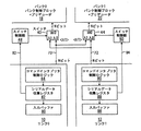
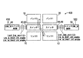
バンク選択制御として機能するためにリンク0 10からスイッチ制御部48、50への入力として接続される制御入力Bnk0<1:0> 49。
リンク0からの制御、アドレスおよびデータをバンク0に与えることを可能にする、スイッチ制御部48からスイッチ40へのLnk_is_Bnk0_ctrl_enable 53。
リンク1からの制御、アドレスおよびデータをバンク0に与えることを可能にする、スイッチ制御部48からスイッチ40へのLnk_os_Bnk0_ctrl_enable 60。
ページバッファから、リンク0に関するリンクロジックブロックに対して読出し関連操作が実行される場合にバンクを選択するために使用される、スイッチ制御部48からスイッチ42へのLnk0_Bnk_slct<1:0>出力64。
バンク選択制御として機能するためにリンク1 12からスイッチ制御部48、50への入力として接続される制御入力Bnk1<1:0> 51。
リンク1からの制御、アドレスおよびデータをバンク1に与えることを可能にする、スイッチ制御部50からスイッチ44へのLnk_is_Bnk1_ctrl_enable 63。
リンク0からの制御、アドレスおよびデータをバンク1に与えることを可能にする、スイッチ制御部50からスイッチ44へのLnk_os_Bnk1_ctrl_enable 65。
ページバッファから、リンク1に関するリンクロジックブロックに対して読出し関連操作が実行される場合にバンクを選択するために使用される、スイッチ制御部50からスイッチ46へのLnk1_Bnk_slct<1:0>出力66。
スイッチ42、46のそれぞれに接続されて示されたバンク0出力60。この出力は、個々の設計に応じて例えば4ビット、8ビットまたは16ビットのパラレル出力とすることができ、リンクブロック内でパラレル/シリアル変換が行われる。あるいは、バンク0内に読出しアクセス用の組込パラレル/シリアル変換器がある場合、この出力はシリアル出力とすることができる。この説明の残りの部分では、この出力を8ビットのパラレル出力と想定する。
スイッチ42、46のそれぞれに接続されて示されたバンク1出力62。出力60に関して上記に説明したのと同様の解説がこの出力についても当てはまる。
スイッチ42とリンク0 10とを相互接続する接続67。
スイッチ46とリンク1 12とを相互接続する接続68。
スイッチ40の個々のスイッチング素子およびスイッチ44の個々のスイッチング素子にそれぞれ接続される、リンク0 10からの複数の出力70。
スイッチ40の個々のスイッチング素子およびスイッチ44の個々のスイッチング素子にそれぞれ接続される、リンク1 12からの複数の出力72。
バンク0 18に接続されるスイッチ40の各スイッチング素子からの個々の出力であり、74で集合的に示す出力。
バンク1 20に接続されるスイッチ44の各スイッチング素子からの個々の出力であり、76で集合的に示す出力。
リンク0用のLnk0_Bank_slct<0>、
各リンク0用のLnk0_Bank_slct<1>、
リンク1用のLnk1_Bank_slct<0>、
各リンク1用のLnk1_Bank_slct<1>、
Lnk_is_Bnk0_ctrl_enable、
Lnk_os_Bnk0_ctrl_enable、
Lnk_is_Bnk1_ctrl_enable、および
Lnk_os_Bnk1_ctrl_enableである。
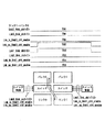
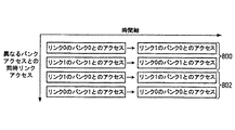
以下に説明する様々なアクセスシナリオは、リンク0からバンク0へのアクセス、リンク0からバンク1へのアクセス、リンク1からバンク1へのアクセス、およびリンク1からバンク0へのアクセスを含む。
・ リンク0の位置(link_id=0)→NAND380の出力が「lnk_is」の結果に影響し、NAND388はロジック的にどんな影響も与えない。その結果はリンク0からのバンク0アクセス→内部にリンク(304A)。
・ リンク1の位置(link_id=1)→NAND388の出力が「lnk_is」の結果に影響し、NAND380はロジック的にどんな影響も与えない。その結果はリンク1からのバンク1アクセス→内部にリンク(304A)。
・ リンク0の位置(link_id=0)→NAND400の出力が「lnk_os」の結果に影響する。→Bk1<0>が入力の1つとしてNAND392にロジック的に接続される。その結果はリンク1からのバンク0アクセス→外部にリンク(304B)。
・ リンク1の位置(link_id=1)→NAND390の出力が「lnk_os」の結果に影響する。→Bk0<1>が入力の1つとしてNAND392にロジック的に接続される。その結果はリンク0からのバンク1アクセス→外部にリンク(304B)。
12 リンク1
14 制御ロジック
16 スイッチングロジック
18 バンク0
20 バンク1
30 デュアルポート構成
32 シングルポート構成
40 スイッチ
42 スイッチ
44 スイッチ
46 スイッチ
48 スイッチ制御部
48 スイッチ
49 Bnk0<1:0>
49 制御入力
50 スイッチ制御部
50 スイッチ
51 Bnk1<1:0>
51 制御入力
53 Lnk_is_Bnk0_ctrl_enable
60 Lnk_os_Bnk0_ctrl_enable
60 バンク0出力
62 バンク1出力
63 Lnk_is_Bnk1_ctrl_enable
65 Lnk_os_Bnk1_ctrl_enable
64 Lnk0_Bnk_slct<1:0>
66 Lnk1_Bnk_slct<1:0>
67 出力
67 接続
68 出力
68 接続
70 出力
72 出力
74 出力
76 出力
80 入力バッファ
82 シリアルデータ収集レジスタ
84 コマンドインタプリタ制御ロジック
86 入力バッファ
88 シリアルデータ収集レジスタ
90 コマンドインタプリタ制御ロジック
92 制御出力
94 制御出力
100 第1のNANDゲート
101 スイッチング素子
102 第2のNANDゲート
103 スイッチング素子
104 第3のNANDゲート
105 out0
110 第1のNANDゲート
112 第2のNANDゲート
114 第3のNANDゲート
115 out1
300 回路
301 無効検査ロジック
302 シングルリンク構成回路
303A 回路
303B 回路
304A スイッチロジック
304B スイッチロジック
305 リンク認識ロジック
306A 保持ロジック
306A 保持回路
306B 保持ロジック
306B 保持回路
307A バンク選択ロジック
307B バンク選択ロジック
350 NANDゲート
352 NANDゲート
354 インバータ
356 NANDゲート
358 NANDゲート
360 インバータ
370 第1のNANDゲート
372 第2のNANDゲート
374 第3のNANDゲート
380 第1のNANDゲート
380 NANDゲート
380 NAND
382 NANDゲート
388 第1のNANDゲート
388 NANDゲート
388 NAND
390 第2のNANDゲート
390 NANDゲート
390 NAND
392 第3のNANDゲート
392 NAND
400 NANDゲート
400 NAND
402 インバータ
403 インバータ
404 NANDゲート
406 インバータ
408 NANDゲート
410 インバータ
Claims (15)
- 第1のリンクと、
第2のリンクと、
第1のバンクと、
第2のバンクと、
前記第1のバンク、前記第2のバンク、前記第1のリンク、および前記第2のリンクの間でデータを切り替えるスイッチング回路と、を含み、
前記スイッチング回路は第1のスイッチングロジック回路を含み、
前記第1のスイッチングロジック回路は、
前記第1のリンクから入力データを受け取るための第1の入力と、
前記第1のリンクについての書込みのためのイネーブルを受け取るための第2の入力と、
前記第2のリンクから入力データを受け取るための第3の入力と、
前記第2のリンクについての書込みのためのイネーブルを受け取るための第4の入力と、
メモリバンクにデータを出力するための出力と、を含む、
メモリデバイス。 - 第2のスイッチングロジック回路をさらに含み、
前記第2のスイッチングロジック回路は、
前記第1のバンクから入力データを受け取るための第1の入力と、
前記第1のバンクからの読出しのためのイネーブルを受け取るための第2の入力と、
前記第2のバンクから入力データを受け取るための第3の入力と、
前記第2のバンクからの読出しのためのイネーブルを受け取るための第4の入力と、
前記第1または第2のバンクから読出されたデータを出力するための出力と、を含む、
請求項1に記載のメモリデバイス。 - 前記第1のスイッチングロジック回路は、
前記第1のリンクからのデータを受け取るための前記第1のスイッチングロジック回路の前記第1の入力と、前記第1のリンクについての書込みのための前記イネーブルを受け取るための前記第1のスイッチングロジック回路の前記第2の入力と、に接続された第1のNANDゲートと、
前記第2のリンクからデータを受け取るための前記第1のスイッチングロジック回路の前記第3の入力と、前記第2のリンクについての書込みのための前記イネーブルを受け取るための前記第1のスイッチングロジック回路の前記第4の入力と、に接続された第2のNANDゲートと、
前記第1のスイッチングロジック回路の前記出力を生成するために、前記第1のNANDゲートの出力と、前記第2のNANDゲートの出力と、に接続された第3のNANDゲートと、を含む、
請求項1に記載のメモリデバイス。 - 前記第2のスイッチングロジック回路は、
前記第1のバンクからのデータを受け取るための前記第2のスイッチングロジック回路の前記第1の入力と、前記第1のバンクからの読出しのための前記イネーブルを受け取るための前記第2のスイッチングロジック回路の前記第2の入力と、に接続された第1のNANDゲートと、
前記第2のバンクからデータを受け取るための前記第2のスイッチングロジック回路の前記第3の入力と、前記第2のバンクからの読出しのための前記イネーブルを受け取るための前記第2のスイッチングロジック回路の前記第4の入力と、に接続された第2のNANDゲートと、
前記第2のスイッチングロジック回路の前記出力を生成するために、前記第1のNANDゲートの出力と、前記第2のNANDゲートの出力と、に接続された第3のNANDゲートと、を含む、
請求項2に記載のメモリデバイス。 - 第2のスイッチングロジック回路をさらに含み、
前記第2のスイッチングロジック回路は、
前記第1のバンクから入力データを受け取るための第1の入力と、
前記第1のバンクからの読出しのためのイネーブルを受け取るための第2の入力と、
前記第2のバンクから入力データを受け取るための第3の入力と、
前記第2のバンクからの読出しのためのイネーブルを受け取るための第4の入力と、
前記第1または第2のバンクから読出されたデータを出力するための出力と、を含み、
前記第2のスイッチングロジック回路は、
前記第1のバンクからのデータを受け取るための前記第2のスイッチングロジック回路の前記第1の入力と、前記第1のバンクからの読出しのための前記イネーブルを受け取るための前記第2のスイッチングロジック回路の前記第2の入力と、に接続された第4のNANDゲートと、
前記第2のバンクからデータを受け取るための前記第2のスイッチングロジック回路の前記第3の入力と、前記第2のバンクからの読出しのための前記イネーブルを受け取るための前記第2のスイッチングロジック回路の前記第4の入力と、に接続された第5のNANDゲートと、
前記第2のスイッチングロジック回路の前記出力を生成するために、前記第1のNANDゲートの出力と、前記第2のNANDゲートの出力と、に接続された第6のNANDゲートと、を含む、
請求項3に記載のメモリデバイス。 - 第1の複数の前記第1のスイッチングロジック回路であって、各々が、前記第1のリンクからのそれぞれのデータと、前記第1のリンクについての書込みのための前記イネーブルと、前記第2のリンクからのそれぞれのデータと、前記第2のリンクについての書込みのための前記イネーブルと、を受け取ることを含む、前記第1の複数の前記第1のスイッチングロジック回路を含み、
前記第1の複数の前記第1のスイッチングロジック回路の各々は、前記第1のバンクへデータを出力するためのそれぞれの出力を有する、
請求項1に記載のメモリデバイス。 - 第1の複数の前記第1のスイッチングロジック回路であって、各々が、前記第1のリンクからのそれぞれのデータと、前記第1のリンクについての書込みのための前記イネーブルと、前記第2のリンクからのそれぞれのデータと、前記第2のリンクについての書込みのための前記イネーブルと、を受け取ることを含み、各々が、前記第2のバンクへデータを出力するためのそれぞれの出力を有する、前記第1の複数の前記第1のスイッチングロジック回路を含む、
請求項1に記載のメモリデバイス。 - 第2の複数の前記第1のスイッチングロジック回路であって、各々が、前記第1のリンクからのそれぞれのデータと、前記第1のリンクについての書込みのための前記イネーブルと、前記第2のリンクからのそれぞれのデータと、前記第2のリンクについての書込みのための前記イネーブルと、を受け取り、各々が、前記第2のバンクへデータを出力するためのそれぞれの出力を有する、前記第2の複数の前記第1のスイッチングロジック回路を含む、
請求項6に記載のメモリデバイス。 - 2つの前記第2のスイッチングロジック回路と、を含み、
前記2つの第2のスイッチングロジック回路の第1の前記出力は前記第1のリンクのためであり、前記2つの第2のスイッチングロジック回路の第2の前記出力は前記第2のリンクのためである、
請求項2に記載のメモリデバイス。 - 各々のリンクは、
前記リンク制御部の少なくとも1つの入力を介して入力コマンドおよび入力データを受け取るための入力バッファと、
入力コマンドおよび入力データをパラレル形式に変換するためのコンバータと、
入力コマンドを解釈するためのコマンドインタプリタと、を含む、
請求項1に記載のメモリデバイス。 - 第1の複数の前記第1のスイッチングロジック回路であって、各々が、前記第1のリンクからのそれぞれのデータと、前記第1のリンクについての書込みのための前記イネーブルと、前記第2のリンクからのそれぞれのデータと、前記第2のリンクについての書込みのための前記イネーブルと、を受け取り、各々が、前記第1のバンクへデータを出力するためのそれぞれの出力を有する、前記第1の複数の前記第1のスイッチングロジック回路と、
第2の複数の前記第1のスイッチングロジック回路であって、各々が、前記第1のリンクからのそれぞれのデータと、前記第1のリンクについての書込みのための前記イネーブルと、前記第2のリンクからのそれぞれのデータと、前記第2のリンクについての書込みのための前記イネーブルと、を受け取り、各々が、前記第2のバンクへデータを出力するためのそれぞれの出力を有する、前記第2の複数の前記第1のスイッチングロジック回路と、
2つの前記第2のスイッチングロジック回路であって、前記2つの第2のスイッチングロジック回路の第1の前記出力は前記第1のリンクのためであり、前記2つの第2のスイッチングロジック回路の第2の前記出力は前記第2のリンクのためである、前記2つの前記第2のスイッチングロジック回路と、を含む、
請求項2に記載のメモリデバイス。 - 第1のリンクと、
第2のリンクと、
第1のバンクと、
第2のバンクと、
前記第1のバンク、前記第2のバンク、前記第1のリンク、および前記第2のリンクとの間でデータを切り替えるスイッチング回路と、を含み、
前記スイッチング回路はスイッチングロジック回路を含み、
前記スイッチングロジック回路は、
前記第1のバンクから入力データを受け取るための第1の入力と、
前記第1のバンクからの読出しのためのイネーブルを受け取るための第2の入力と、
前記第2のバンクから入力データを受け取るための第3の入力と、
前記第2のバンクからの読出しのためのイネーブルを受け取るための第4の入力と、
前記第1または第2のバンクから読出されたデータを出力するための出力と、を含む、
メモリデバイス。 - 前記スイッチングロジック回路は、
前記第1のバンクからのデータを受け取るための前記スイッチングロジック回路の前記第1の入力と、前記第1のバンクからの読出しのための前記イネーブルを受け取るための前記スイッチングロジック回路の前記第2の入力と、に接続された第1のNANDゲートと、
前記第2のバンクからデータを受け取るための前記スイッチングロジック回路の前記第3の入力と、前記第2のバンクからの読出しのための前記イネーブルを受け取るための前記スイッチングロジック回路の前記第4の入力と、に接続された第2のNANDゲートと、
前記スイッチングロジック回路の前記出力を生成するために、前記第1のNANDゲートの出力と、前記第2のNANDゲートの出力と、に接続された第3のNANDゲートと、を含む、
請求項12に記載のメモリデバイス。 - 2つの前記スイッチングロジック回路と、を含み、
前記2つのスイッチングロジック回路の第1の前記出力は前記第1のリンクのためであり、前記2つのスイッチングロジック回路の第2の前記出力は前記第2のリンクのためである、
請求項12に記載のメモリデバイス。 - 各々のリンクは、
前記リンク制御部の少なくとも1つの入力を介して入力コマンドおよび入力データを受け取るための入力バッファと、
入力コマンドおよび入力データをパラレル形式に変換するためのコンバータと、
入力コマンドを解釈するためのコマンドインタプリタと、を含む、
請求項12に記載のメモリデバイス。
Applications Claiming Priority (2)
| Application Number | Priority Date | Filing Date | Title |
|---|---|---|---|
| US11/643,850 | 2006-12-22 | ||
| US11/643,850 US7747833B2 (en) | 2005-09-30 | 2006-12-22 | Independent link and bank selection |
Related Parent Applications (1)
| Application Number | Title | Priority Date | Filing Date |
|---|---|---|---|
| JP2012136668A Division JP5591284B2 (ja) | 2006-12-22 | 2012-06-18 | 独立リンクおよびバンク選択 |
Publications (1)
| Publication Number | Publication Date |
|---|---|
| JP2014199679A true JP2014199679A (ja) | 2014-10-23 |
Family
ID=39562054
Family Applications (3)
| Application Number | Title | Priority Date | Filing Date |
|---|---|---|---|
| JP2009541717A Expired - Fee Related JP5467573B2 (ja) | 2006-12-22 | 2007-12-21 | 独立リンクおよびバンク選択 |
| JP2012136668A Expired - Fee Related JP5591284B2 (ja) | 2006-12-22 | 2012-06-18 | 独立リンクおよびバンク選択 |
| JP2014153970A Pending JP2014199679A (ja) | 2006-12-22 | 2014-07-29 | メモリデバイス |
Family Applications Before (2)
| Application Number | Title | Priority Date | Filing Date |
|---|---|---|---|
| JP2009541717A Expired - Fee Related JP5467573B2 (ja) | 2006-12-22 | 2007-12-21 | 独立リンクおよびバンク選択 |
| JP2012136668A Expired - Fee Related JP5591284B2 (ja) | 2006-12-22 | 2012-06-18 | 独立リンクおよびバンク選択 |
Country Status (7)
| Country | Link |
|---|---|
| US (4) | US7747833B2 (ja) |
| EP (1) | EP2126918A4 (ja) |
| JP (3) | JP5467573B2 (ja) |
| KR (2) | KR101370711B1 (ja) |
| CN (2) | CN103366799A (ja) |
| TW (1) | TWI536394B (ja) |
| WO (1) | WO2008077244A1 (ja) |
Cited By (1)
| Publication number | Priority date | Publication date | Assignee | Title |
|---|---|---|---|---|
| US10496569B2 (en) | 2017-09-19 | 2019-12-03 | Kabushiki Kaisha Toshiba | Semiconductor integrated circuit |
Families Citing this family (30)
| Publication number | Priority date | Publication date | Assignee | Title |
|---|---|---|---|---|
| US7747833B2 (en) | 2005-09-30 | 2010-06-29 | Mosaid Technologies Incorporated | Independent link and bank selection |
| EP1932158A4 (en) | 2005-09-30 | 2008-10-15 | Mosaid Technologies Inc | MEMORY WITH OUTPUT CONTROL |
| US7652922B2 (en) | 2005-09-30 | 2010-01-26 | Mosaid Technologies Incorporated | Multiple independent serial link memory |
| US20080005257A1 (en) * | 2006-06-29 | 2008-01-03 | Kestrelink Corporation | Dual processor based digital media player architecture with network support |
| US8825939B2 (en) * | 2007-12-12 | 2014-09-02 | Conversant Intellectual Property Management Inc. | Semiconductor memory device suitable for interconnection in a ring topology |
| US8139390B2 (en) * | 2008-07-08 | 2012-03-20 | Mosaid Technologies Incorporated | Mixed data rates in memory devices and systems |
| EP2329496A4 (en) | 2008-09-30 | 2012-06-13 | Mosaid Technologies Inc | SERIAL SWITCHED STORAGE SYSTEM WITH OUTPUT DELAY SETTING |
| US8161313B2 (en) * | 2008-09-30 | 2012-04-17 | Mosaid Technologies Incorporated | Serial-connected memory system with duty cycle correction |
| US8181056B2 (en) * | 2008-09-30 | 2012-05-15 | Mosaid Technologies Incorporated | Serial-connected memory system with output delay adjustment |
| US8134852B2 (en) * | 2008-10-14 | 2012-03-13 | Mosaid Technologies Incorporated | Bridge device architecture for connecting discrete memory devices to a system |
| US7957173B2 (en) * | 2008-10-14 | 2011-06-07 | Mosaid Technologies Incorporated | Composite memory having a bridging device for connecting discrete memory devices to a system |
| US20100115172A1 (en) * | 2008-11-04 | 2010-05-06 | Mosaid Technologies Incorporated | Bridge device having a virtual page buffer |
| US8549209B2 (en) * | 2008-11-04 | 2013-10-01 | Mosaid Technologies Incorporated | Bridging device having a configurable virtual page size |
| US8472199B2 (en) | 2008-11-13 | 2013-06-25 | Mosaid Technologies Incorporated | System including a plurality of encapsulated semiconductor chips |
| KR101006748B1 (ko) * | 2009-01-29 | 2011-01-10 | (주)인디링스 | 패드들의 동시 스위칭을 제어하는 고체 상태 디스크를 위한컨트롤러 |
| TW201044371A (en) * | 2009-06-15 | 2010-12-16 | Novatek Microelectronics Corp | Memory architecture of display device and reading method thereof |
| US8484428B2 (en) * | 2009-07-30 | 2013-07-09 | Micron Technology, Inc. | Enhanced block copy |
| US8582382B2 (en) * | 2010-03-23 | 2013-11-12 | Mosaid Technologies Incorporated | Memory system having a plurality of serially connected devices |
| US8843692B2 (en) | 2010-04-27 | 2014-09-23 | Conversant Intellectual Property Management Inc. | System of interconnected nonvolatile memories having automatic status packet |
| US8533403B1 (en) | 2010-09-30 | 2013-09-10 | Apple Inc. | Arbitration unit for memory system |
| WO2012082480A2 (en) * | 2010-12-14 | 2012-06-21 | Rambus Inc. | Multi-die dram banks arrangement and wiring |
| JP5864957B2 (ja) * | 2011-08-31 | 2016-02-17 | ルネサスエレクトロニクス株式会社 | 半導体装置 |
| US9974686B2 (en) | 2012-06-26 | 2018-05-22 | Synergetics, Inc. | Ophthalmic surgical fluid handling cassette |
| US9471484B2 (en) | 2012-09-19 | 2016-10-18 | Novachips Canada Inc. | Flash memory controller having dual mode pin-out |
| US9361973B2 (en) | 2013-10-28 | 2016-06-07 | Cypress Semiconductor Corporation | Multi-channel, multi-bank memory with wide data input/output |
| US9933980B2 (en) * | 2014-02-24 | 2018-04-03 | Toshiba Memory Corporation | NAND raid controller for connection between an SSD controller and multiple non-volatile storage units |
| KR102346629B1 (ko) * | 2014-12-05 | 2022-01-03 | 삼성전자주식회사 | 메모리 접근 제어 방법 및 장치 |
| US9747042B2 (en) * | 2015-06-30 | 2017-08-29 | International Business Machines Corporation | Statistic-based isolation of lethargic drives |
| US9690494B2 (en) * | 2015-07-21 | 2017-06-27 | Qualcomm Incorporated | Managing concurrent access to multiple storage bank domains by multiple interfaces |
| US10140044B2 (en) | 2016-03-31 | 2018-11-27 | Qualcomm Incorporated | Efficient memory bank design |
Citations (4)
| Publication number | Priority date | Publication date | Assignee | Title |
|---|---|---|---|---|
| JPH11282794A (ja) * | 1998-03-27 | 1999-10-15 | Chokosoku Network Computer Gijutsu Kenkyusho:Kk | メモリ・アクセス方式 |
| JP2000231535A (ja) * | 1998-11-13 | 2000-08-22 | Infineon Technol North America Corp | メモリカップリングユニットを持つデータ処理装置 |
| JP2002298595A (ja) * | 2001-03-28 | 2002-10-11 | Toshiba Corp | 半導体記憶装置 |
| WO2003009301A1 (en) * | 2001-07-17 | 2003-01-30 | Mitsubishi Denki Kabushiki Kaisha | Storage device |
Family Cites Families (132)
| Publication number | Priority date | Publication date | Assignee | Title |
|---|---|---|---|---|
| US4174536A (en) | 1977-01-21 | 1979-11-13 | Massachusetts Institute Of Technology | Digital communications controller with firmware control |
| US4617566A (en) | 1983-12-15 | 1986-10-14 | Teleplex Corporation | Addressable-port, daisy chain telemetry system with self-test capability |
| DE3586523T2 (de) | 1984-10-17 | 1993-01-07 | Fujitsu Ltd | Halbleiterspeicheranordnung mit einer seriellen dateneingangs- und ausgangsschaltung. |
| US4683555A (en) | 1985-01-22 | 1987-07-28 | Texas Instruments Incorporated | Serial accessed semiconductor memory with reconfigureable shift registers |
| US4714536A (en) | 1985-08-26 | 1987-12-22 | Varian Associates, Inc. | Planar magnetron sputtering device with combined circumferential and radial movement of magnetic fields |
| JPS6289149A (ja) * | 1985-10-15 | 1987-04-23 | Agency Of Ind Science & Technol | 多ポ−トメモリシステム |
| JPS62152050A (ja) | 1985-12-26 | 1987-07-07 | Nec Corp | 半導体メモリ |
| JPS63113624A (ja) | 1986-10-30 | 1988-05-18 | Tokyo Electric Co Ltd | 電子秤のプリンタインタ−フエ−ス |
| DE69030858T2 (de) | 1989-03-15 | 1998-01-29 | Oki Electric Ind Co Ltd | Serielleingabe-parallelausgabe-umwandlungsschaltung |
| US5126808A (en) | 1989-10-23 | 1992-06-30 | Advanced Micro Devices, Inc. | Flash EEPROM array with paged erase architecture |
| US5175819A (en) | 1990-03-28 | 1992-12-29 | Integrated Device Technology, Inc. | Cascadable parallel to serial converter using tap shift registers and data shift registers while receiving input data from FIFO buffer |
| US5243703A (en) | 1990-04-18 | 1993-09-07 | Rambus, Inc. | Apparatus for synchronously generating clock signals in a data processing system |
| US5204669A (en) | 1990-08-30 | 1993-04-20 | Datacard Corporation | Automatic station identification where function modules automatically initialize |
| US5319598A (en) | 1990-12-10 | 1994-06-07 | Hughes Aircraft Company | Nonvolatile serially programmable devices |
| US5132635A (en) | 1991-03-05 | 1992-07-21 | Ast Research, Inc. | Serial testing of removable circuit boards on a backplane bus |
| JP2673390B2 (ja) * | 1991-03-13 | 1997-11-05 | 三菱電機株式会社 | マルチポートメモリ |
| JPH0776942B2 (ja) | 1991-04-22 | 1995-08-16 | インターナショナル・ビジネス・マシーンズ・コーポレイション | マルチプロセッサ・システムおよびそのデータ伝送装置 |
| US5430859A (en) | 1991-07-26 | 1995-07-04 | Sundisk Corporation | Solid state memory system including plural memory chips and a serialized bus |
| US6230233B1 (en) | 1991-09-13 | 2001-05-08 | Sandisk Corporation | Wear leveling techniques for flash EEPROM systems |
| KR950000761B1 (ko) | 1992-01-15 | 1995-01-28 | 삼성전자 주식회사 | 직렬 입력신호의 동기회로 |
| JP3088180B2 (ja) | 1992-03-26 | 2000-09-18 | 日本電気アイシーマイコンシステム株式会社 | シリアル入力インタフェース回路 |
| KR960000616B1 (ko) | 1993-01-13 | 1996-01-10 | 삼성전자주식회사 | 불휘발성 반도체 메모리 장치 |
| JPH06275069A (ja) | 1993-03-20 | 1994-09-30 | Hitachi Ltd | シリアルメモリ |
| US5365484A (en) | 1993-08-23 | 1994-11-15 | Advanced Micro Devices, Inc. | Independent array grounds for flash EEPROM array with paged erase architechture |
| JPH0793219A (ja) | 1993-09-20 | 1995-04-07 | Olympus Optical Co Ltd | 情報処理装置 |
| US5602780A (en) | 1993-10-20 | 1997-02-11 | Texas Instruments Incorporated | Serial to parallel and parallel to serial architecture for a RAM based FIFO memory |
| US5452259A (en) | 1993-11-15 | 1995-09-19 | Micron Technology Inc. | Multiport memory with pipelined serial input |
| US5404460A (en) | 1994-01-28 | 1995-04-04 | Vlsi Technology, Inc. | Method for configuring multiple identical serial I/O devices to unique addresses through a serial bus |
| US5475854A (en) | 1994-01-28 | 1995-12-12 | Vlsi Technology, Inc. | Serial bus I/O system and method for serializing interrupt requests and DMA requests in a computer system |
| US5596724A (en) | 1994-02-04 | 1997-01-21 | Advanced Micro Devices | Input/output data port with a parallel and serial interface |
| JPH07319755A (ja) * | 1994-05-25 | 1995-12-08 | Nippon Telegr & Teleph Corp <Ntt> | 複数ポートメモリ |
| DE4429433C1 (de) | 1994-08-19 | 1995-10-26 | Siemens Ag | Adreßzuordnungsverfahren |
| US5473566A (en) | 1994-09-12 | 1995-12-05 | Cirrus Logic, Inc. | Memory architecture and devices, systems and methods utilizing the same |
| KR0142367B1 (ko) | 1995-02-04 | 1998-07-15 | 김광호 | 열 리던던씨를 가지는 불휘발성 반도체 메모리의 소거 검증회로 |
| JPH08221319A (ja) * | 1995-02-13 | 1996-08-30 | Hitachi Ltd | 半導体記憶装置 |
| US5636342A (en) | 1995-02-17 | 1997-06-03 | Dell Usa, L.P. | Systems and method for assigning unique addresses to agents on a system management bus |
| US5729683A (en) | 1995-05-18 | 1998-03-17 | Compaq Computer Corporation | Programming memory devices through the parallel port of a computer system |
| US5594694A (en) | 1995-07-28 | 1997-01-14 | Micron Quantum Devices, Inc. | Memory circuit with switch for selectively connecting an input/output pad directly to a nonvolatile memory cell |
| US5742840A (en) | 1995-08-16 | 1998-04-21 | Microunity Systems Engineering, Inc. | General purpose, multiple precision parallel operation, programmable media processor |
| US5835935A (en) | 1995-09-13 | 1998-11-10 | Lexar Media, Inc. | Method of and architecture for controlling system data with automatic wear leveling in a semiconductor non-volatile mass storage memory |
| JPH0991197A (ja) | 1995-09-22 | 1997-04-04 | Sharp Corp | データ転送制御装置 |
| JP3693721B2 (ja) | 1995-11-10 | 2005-09-07 | Necエレクトロニクス株式会社 | フラッシュメモリ内蔵マイクロコンピュータ及びそのテスト方法 |
| TW307869B (en) | 1995-12-20 | 1997-06-11 | Toshiba Co Ltd | Semiconductor memory |
| KR100211760B1 (ko) | 1995-12-28 | 1999-08-02 | 윤종용 | 멀티뱅크 구조를 갖는 반도체 메모리 장치의 데이타 입출력 경로 제어회로 |
| KR0170723B1 (ko) | 1995-12-29 | 1999-03-30 | 김광호 | 단일 ras 신호에 의해 동시 동작이 가능한 이중 뱅크를 갖는 반도체 메모리 장치 |
| US5828899A (en) | 1996-01-04 | 1998-10-27 | Compaq Computer Corporation | System for peripheral devices recursively generating unique addresses based on the number of devices connected dependent upon the relative position to the port |
| WO1997030395A1 (fr) * | 1996-02-16 | 1997-08-21 | Hitachi, Ltd. | Memoire a acces multiples et processeur de donnees procurant l'acces a cette memoire |
| JPH09231740A (ja) | 1996-02-21 | 1997-09-05 | Nec Corp | 半導体記憶装置 |
| US5941974A (en) | 1996-11-29 | 1999-08-24 | Motorola, Inc. | Serial interface with register selection which uses clock counting, chip select pulsing, and no address bits |
| US6493347B2 (en) * | 1996-12-16 | 2002-12-10 | Juniper Networks, Inc. | Memory organization in a switching device |
| US6075743A (en) * | 1996-12-26 | 2000-06-13 | Rambus Inc. | Method and apparatus for sharing sense amplifiers between memory banks |
| KR100243335B1 (ko) | 1996-12-31 | 2000-02-01 | 김영환 | 독립적인 리프레쉬 수단을 가지는 데이지 체인 구조의 반도체 장치 |
| KR100272037B1 (ko) | 1997-02-27 | 2000-12-01 | 니시무로 타이죠 | 불휘발성 반도체 기억 장치 |
| US5900021A (en) | 1997-04-04 | 1999-05-04 | United Memories, Inc. | Pad input select circuit for use with bond options |
| GB2329792A (en) | 1997-08-20 | 1999-03-31 | Nokia Telecommunications Oy | Identification signals enable a transceiver module to correctly configure itself to an attached functional module |
| JPH1166841A (ja) | 1997-08-22 | 1999-03-09 | Mitsubishi Electric Corp | 半導体記憶装置 |
| KR100240873B1 (ko) | 1997-08-26 | 2000-01-15 | 윤종용 | 송수신 겸용의 레지스터를 갖는 직렬인터페이스장치 |
| JP4039532B2 (ja) | 1997-10-02 | 2008-01-30 | 株式会社ルネサステクノロジ | 半導体集積回路装置 |
| US5937425A (en) | 1997-10-16 | 1999-08-10 | M-Systems Flash Disk Pioneers Ltd. | Flash file system optimized for page-mode flash technologies |
| US6148364A (en) | 1997-12-30 | 2000-11-14 | Netlogic Microsystems, Inc. | Method and apparatus for cascading content addressable memory devices |
| US6002638A (en) | 1998-01-20 | 1999-12-14 | Microchip Technology Incorporated | Memory device having a switchable clock output and method therefor |
| US6453365B1 (en) | 1998-02-11 | 2002-09-17 | Globespanvirata, Inc. | Direct memory access controller having decode circuit for compact instruction format |
| GB2339044B (en) | 1998-03-02 | 2003-06-04 | Lexar Media Inc | Flash memory card with enhanced operating mode detection and user-friendly interfacing system |
| US6016270A (en) | 1998-03-06 | 2000-01-18 | Alliance Semiconductor Corporation | Flash memory architecture that utilizes a time-shared address bus scheme and separate memory cell access paths for simultaneous read/write operations |
| US6085290A (en) | 1998-03-10 | 2000-07-04 | Nexabit Networks, Llc | Method of and apparatus for validating data read out of a multi port internally cached dynamic random access memory (AMPIC DRAM) |
| US6144576A (en) | 1998-08-19 | 2000-11-07 | Intel Corporation | Method and apparatus for implementing a serial memory architecture |
| US5995417A (en) | 1998-10-20 | 1999-11-30 | Advanced Micro Devices, Inc. | Scheme for page erase and erase verify in a non-volatile memory array |
| JP4601737B2 (ja) | 1998-10-28 | 2010-12-22 | 株式会社東芝 | メモリ混載ロジックlsi |
| JP2000149564A (ja) | 1998-10-30 | 2000-05-30 | Mitsubishi Electric Corp | 半導体記憶装置 |
| US6216178B1 (en) | 1998-11-16 | 2001-04-10 | Infineon Technologies Ag | Methods and apparatus for detecting the collision of data on a data bus in case of out-of-order memory accesses of different times of memory access execution |
| US6304921B1 (en) | 1998-12-07 | 2001-10-16 | Motorola Inc. | System for serial peripheral interface with embedded addressing circuit for providing portion of an address for peripheral devices |
| KR100284742B1 (ko) | 1998-12-28 | 2001-04-02 | 윤종용 | 입출력 센스앰프의 개수가 최소화된 메모리장치 |
| JP3853537B2 (ja) | 1999-04-30 | 2006-12-06 | 株式会社日立製作所 | 半導体メモリファイルシステム |
| US6176135B1 (en) * | 1999-07-27 | 2001-01-23 | Marc Dubois | System and method for laser-ultrasonic frequency control using optimal wavelength tuning |
| US7130958B2 (en) | 2003-12-02 | 2006-10-31 | Super Talent Electronics, Inc. | Serial interface to flash-memory chip using PCI-express-like packets and packed data for partial-page writes |
| JP3892655B2 (ja) | 1999-09-17 | 2007-03-14 | 株式会社東芝 | 半導体集積回路装置 |
| US6680904B1 (en) | 1999-12-27 | 2004-01-20 | Orckit Communications Ltd. | Bi-directional chaining of network access ports |
| US20050160218A1 (en) | 2004-01-20 | 2005-07-21 | Sun-Teck See | Highly integrated mass storage device with an intelligent flash controller |
| US6442098B1 (en) | 2000-02-08 | 2002-08-27 | Alliance Semiconductor | High performance multi-bank compact synchronous DRAM architecture |
| US6988154B2 (en) | 2000-03-10 | 2006-01-17 | Arc International | Memory interface and method of interfacing between functional entities |
| US6816933B1 (en) | 2000-05-17 | 2004-11-09 | Silicon Laboratories, Inc. | Serial device daisy chaining method and apparatus |
| US6535948B1 (en) | 2000-05-31 | 2003-03-18 | Agere Systems Inc. | Serial interface unit |
| US6317350B1 (en) | 2000-06-16 | 2001-11-13 | Netlogic Microsystems, Inc. | Hierarchical depth cascading of content addressable memory devices |
| US6356487B1 (en) | 2000-08-23 | 2002-03-12 | Micron Technology, Inc. | Memory device having data path containing dual mode flip-flop used for normal operation and for internal testing |
| US6754807B1 (en) | 2000-08-31 | 2004-06-22 | Stmicroelectronics, Inc. | System and method for managing vertical dependencies in a digital signal processor |
| GB2370667B (en) | 2000-09-05 | 2003-02-12 | Samsung Electronics Co Ltd | Semiconductor memory device having altered clock frequency for address and/or command signals, and memory module and system having the same |
| US6317352B1 (en) | 2000-09-18 | 2001-11-13 | Intel Corporation | Apparatus for implementing a buffered daisy chain connection between a memory controller and memory modules |
| US6853557B1 (en) | 2000-09-20 | 2005-02-08 | Rambus, Inc. | Multi-channel memory architecture |
| US6658509B1 (en) | 2000-10-03 | 2003-12-02 | Intel Corporation | Multi-tier point-to-point ring memory interface |
| FR2816751A1 (fr) | 2000-11-15 | 2002-05-17 | St Microelectronics Sa | Memoire flash effacable par page |
| JP2002236611A (ja) | 2000-12-04 | 2002-08-23 | Hitachi Ltd | 半導体装置と情報処理システム |
| US6642986B2 (en) | 2001-04-13 | 2003-11-04 | Koninklijke Philips Electronics N.V. | Liquid crystal display device having uniform integrated spacers |
| US6757761B1 (en) * | 2001-05-08 | 2004-06-29 | Tera Force Technology Corp. | Multi-processor architecture for parallel signal and image processing |
| US6732221B2 (en) | 2001-06-01 | 2004-05-04 | M-Systems Flash Disk Pioneers Ltd | Wear leveling of static areas in flash memory |
| US6996644B2 (en) | 2001-06-06 | 2006-02-07 | Conexant Systems, Inc. | Apparatus and methods for initializing integrated circuit addresses |
| US6823402B2 (en) | 2001-11-14 | 2004-11-23 | Texas Instruments Incorporated | Apparatus and method for distribution of signals from a high level data link controller to multiple digital signal processor cores |
| KR100413762B1 (ko) | 2001-07-02 | 2003-12-31 | 삼성전자주식회사 | 뱅크 수를 가변할 수 있는 반도체 장치 및 그 방법 |
| JP2003036681A (ja) | 2001-07-23 | 2003-02-07 | Hitachi Ltd | 不揮発性記憶装置 |
| US6928501B2 (en) | 2001-10-15 | 2005-08-09 | Silicon Laboratories, Inc. | Serial device daisy chaining method and apparatus |
| US6914901B1 (en) | 2001-12-05 | 2005-07-05 | Cisco Technology, Inc. | System and method for communicating using multiple memory banks |
| US6763426B1 (en) | 2001-12-27 | 2004-07-13 | Cypress Semiconductor Corporation | Cascadable content addressable memory (CAM) device and architecture |
| JP2003263363A (ja) * | 2002-03-08 | 2003-09-19 | Ricoh Co Ltd | メモリ制御回路 |
| US6906978B2 (en) | 2002-03-19 | 2005-06-14 | Intel Corporation | Flexible integrated memory |
| US7073022B2 (en) | 2002-05-23 | 2006-07-04 | International Business Machines Corporation | Serial interface for a data storage array |
| US7062601B2 (en) | 2002-06-28 | 2006-06-13 | Mosaid Technologies Incorporated | Method and apparatus for interconnecting content addressable memory devices |
| KR100499686B1 (ko) | 2002-07-23 | 2005-07-07 | 주식회사 디지털웨이 | 메모리 확장 가능한 휴대용 플래쉬 메모리 장치 |
| CA2396632A1 (en) | 2002-07-31 | 2004-01-31 | Mosaid Technologies Incorporated | Cam diamond cascade architecture |
| KR100487539B1 (ko) | 2002-09-02 | 2005-05-03 | 삼성전자주식회사 | 직렬 에이티에이 케이블과 연결되는 불휘발성 반도체메모리 장치 |
| EP1424635B1 (en) | 2002-11-28 | 2008-10-29 | STMicroelectronics S.r.l. | Non volatile memory device architecture, for instance a flash kind, having a serial communication interface |
| KR100493884B1 (ko) | 2003-01-09 | 2005-06-10 | 삼성전자주식회사 | 시리얼 플래시 메모리에서의 현지 실행을 위한 제어 장치및 그 방법, 이를 이용한 플래시 메모리 칩 |
| US7308524B2 (en) | 2003-01-13 | 2007-12-11 | Silicon Pipe, Inc | Memory chain |
| US7242684B2 (en) * | 2003-02-07 | 2007-07-10 | Fujitsu Limited | Architecture for switching packets in a high-speed switching environment |
| US20040199721A1 (en) | 2003-03-12 | 2004-10-07 | Power Data Communication Co., Ltd. | Multi-transmission interface memory card |
| US7571287B2 (en) | 2003-03-13 | 2009-08-04 | Marvell World Trade Ltd. | Multiport memory architecture, devices and systems including the same, and methods of using the same |
| KR101095025B1 (ko) | 2003-05-13 | 2011-12-20 | 어드밴스드 마이크로 디바이시즈, 인코포레이티드 | 직렬 메모리 상호접속부를 통해 복수의 메모리 모듈에결합된 호스트를 포함하는 시스템 |
| JP4256210B2 (ja) * | 2003-06-12 | 2009-04-22 | 株式会社半導体理工学研究センター | 同期バンク型メモリ |
| JP4156986B2 (ja) | 2003-06-30 | 2008-09-24 | 株式会社東芝 | 不揮発性半導体記憶装置 |
| JP2005025473A (ja) | 2003-07-01 | 2005-01-27 | Matsushita Electric Ind Co Ltd | 複合入出力装置 |
| US7031221B2 (en) | 2003-12-30 | 2006-04-18 | Intel Corporation | Fixed phase clock and strobe signals in daisy chained chips |
| WO2005069150A1 (en) | 2004-01-20 | 2005-07-28 | Trek 2000 International Ltd. | Portable data storage device using multiple memory devices |
| US7930540B2 (en) | 2004-01-22 | 2011-04-19 | Mcafee, Inc. | Cryptographic policy enforcement |
| JP2005260321A (ja) * | 2004-03-09 | 2005-09-22 | Nec Corp | ラベルパスネットワークの迂回制御方式 |
| JP4697924B2 (ja) | 2004-06-07 | 2011-06-08 | キヤノン株式会社 | データ転送方法 |
| KR100705221B1 (ko) | 2004-09-03 | 2007-04-06 | 에스티마이크로일렉트로닉스 엔.브이. | 플래쉬 메모리 소자 및 이를 이용한 플래쉬 메모리 셀의소거 방법 |
| US6950325B1 (en) | 2004-10-07 | 2005-09-27 | Winbond Electronics Corporation | Cascade-connected ROM |
| US8041879B2 (en) | 2005-02-18 | 2011-10-18 | Sandisk Il Ltd | Flash memory backup system and method |
| JP2006260127A (ja) * | 2005-03-17 | 2006-09-28 | Hiroshima Univ | 結合網およびそれを用いたマルチポートメモリ |
| JP2006260124A (ja) | 2005-03-17 | 2006-09-28 | Hitachi Ltd | データバックアップ方法 |
| ATE520086T1 (de) | 2005-06-30 | 2011-08-15 | Imec | Speicheranordnung für mehrprozessorsysteme |
| US7747833B2 (en) | 2005-09-30 | 2010-06-29 | Mosaid Technologies Incorporated | Independent link and bank selection |
| US7652922B2 (en) | 2005-09-30 | 2010-01-26 | Mosaid Technologies Incorporated | Multiple independent serial link memory |
| US8407395B2 (en) | 2006-08-22 | 2013-03-26 | Mosaid Technologies Incorporated | Scalable memory system |
-
2006
- 2006-12-22 US US11/643,850 patent/US7747833B2/en active Active
-
2007
- 2007-12-21 KR KR1020097015434A patent/KR101370711B1/ko active Active
- 2007-12-21 TW TW103125753A patent/TWI536394B/zh active
- 2007-12-21 CN CN201310246837XA patent/CN103366799A/zh active Pending
- 2007-12-21 EP EP07855602A patent/EP2126918A4/en not_active Withdrawn
- 2007-12-21 WO PCT/CA2007/002320 patent/WO2008077244A1/en not_active Ceased
- 2007-12-21 JP JP2009541717A patent/JP5467573B2/ja not_active Expired - Fee Related
- 2007-12-21 KR KR1020137018555A patent/KR101392593B1/ko active Active
- 2007-12-21 CN CN2007800515754A patent/CN101611453B/zh active Active
-
2010
- 2010-04-09 US US12/757,406 patent/US7945755B2/en not_active Expired - Lifetime
-
2011
- 2011-03-31 US US13/077,122 patent/US8285960B2/en not_active Expired - Fee Related
-
2012
- 2012-06-18 JP JP2012136668A patent/JP5591284B2/ja not_active Expired - Fee Related
- 2012-09-10 US US13/608,605 patent/US8738879B2/en not_active Expired - Lifetime
-
2014
- 2014-07-29 JP JP2014153970A patent/JP2014199679A/ja active Pending
Patent Citations (4)
| Publication number | Priority date | Publication date | Assignee | Title |
|---|---|---|---|---|
| JPH11282794A (ja) * | 1998-03-27 | 1999-10-15 | Chokosoku Network Computer Gijutsu Kenkyusho:Kk | メモリ・アクセス方式 |
| JP2000231535A (ja) * | 1998-11-13 | 2000-08-22 | Infineon Technol North America Corp | メモリカップリングユニットを持つデータ処理装置 |
| JP2002298595A (ja) * | 2001-03-28 | 2002-10-11 | Toshiba Corp | 半導体記憶装置 |
| WO2003009301A1 (en) * | 2001-07-17 | 2003-01-30 | Mitsubishi Denki Kabushiki Kaisha | Storage device |
Cited By (1)
| Publication number | Priority date | Publication date | Assignee | Title |
|---|---|---|---|---|
| US10496569B2 (en) | 2017-09-19 | 2019-12-03 | Kabushiki Kaisha Toshiba | Semiconductor integrated circuit |
Also Published As
| Publication number | Publication date |
|---|---|
| KR101370711B1 (ko) | 2014-03-06 |
| US20110179245A1 (en) | 2011-07-21 |
| KR101392593B1 (ko) | 2014-05-08 |
| US7945755B2 (en) | 2011-05-17 |
| CN103366799A (zh) | 2013-10-23 |
| EP2126918A1 (en) | 2009-12-02 |
| JP2012178190A (ja) | 2012-09-13 |
| JP5467573B2 (ja) | 2014-04-09 |
| US20070143677A1 (en) | 2007-06-21 |
| WO2008077244A1 (en) | 2008-07-03 |
| CN101611453A (zh) | 2009-12-23 |
| US8285960B2 (en) | 2012-10-09 |
| US20130003470A1 (en) | 2013-01-03 |
| US7747833B2 (en) | 2010-06-29 |
| TW201442039A (zh) | 2014-11-01 |
| TWI536394B (zh) | 2016-06-01 |
| JP2010514018A (ja) | 2010-04-30 |
| JP5591284B2 (ja) | 2014-09-17 |
| US8738879B2 (en) | 2014-05-27 |
| KR20130095316A (ko) | 2013-08-27 |
| KR20090097199A (ko) | 2009-09-15 |
| CN101611453B (zh) | 2013-07-10 |
| US20100199057A1 (en) | 2010-08-05 |
| EP2126918A4 (en) | 2010-01-27 |
Similar Documents
| Publication | Publication Date | Title |
|---|---|---|
| JP5591284B2 (ja) | 独立リンクおよびバンク選択 | |
| JP5426396B2 (ja) | 直列および並列モードを有するメモリシステムおよび方法 | |
| US8493808B2 (en) | Data flow control in multiple independent port | |
| KR101547076B1 (ko) | 데이지 체인 캐스케이딩 장치 | |
| TWI460736B (zh) | 獨立連結與記憶庫選擇 | |
| US20080098152A1 (en) | Method and apparatus for configuring a memory device | |
| JP2000311500A (ja) | 半導体記憶装置 | |
| HK1187733A (en) | Memory system and method with serial and parallel modes |
Legal Events
| Date | Code | Title | Description |
|---|---|---|---|
| A621 | Written request for application examination |
Free format text: JAPANESE INTERMEDIATE CODE: A621 Effective date: 20140729 |
|
| RD03 | Notification of appointment of power of attorney |
Free format text: JAPANESE INTERMEDIATE CODE: A7423 Effective date: 20140926 |
|
| RD04 | Notification of resignation of power of attorney |
Free format text: JAPANESE INTERMEDIATE CODE: A7424 Effective date: 20150217 |
|
| RD04 | Notification of resignation of power of attorney |
Free format text: JAPANESE INTERMEDIATE CODE: A7424 Effective date: 20150428 |
|
| RD03 | Notification of appointment of power of attorney |
Free format text: JAPANESE INTERMEDIATE CODE: A7423 Effective date: 20150512 |
|
| RD04 | Notification of resignation of power of attorney |
Free format text: JAPANESE INTERMEDIATE CODE: A7424 Effective date: 20150430 |
|
| A977 | Report on retrieval |
Free format text: JAPANESE INTERMEDIATE CODE: A971007 Effective date: 20150610 |
|
| A131 | Notification of reasons for refusal |
Free format text: JAPANESE INTERMEDIATE CODE: A131 Effective date: 20150707 |
|
| A601 | Written request for extension of time |
Free format text: JAPANESE INTERMEDIATE CODE: A601 Effective date: 20150924 |
|
| A02 | Decision of refusal |
Free format text: JAPANESE INTERMEDIATE CODE: A02 Effective date: 20160308 |