JP2020004845A - Wiring board - Google Patents
Wiring board Download PDFInfo
- Publication number
- JP2020004845A JP2020004845A JP2018122894A JP2018122894A JP2020004845A JP 2020004845 A JP2020004845 A JP 2020004845A JP 2018122894 A JP2018122894 A JP 2018122894A JP 2018122894 A JP2018122894 A JP 2018122894A JP 2020004845 A JP2020004845 A JP 2020004845A
- Authority
- JP
- Japan
- Prior art keywords
- metal wiring
- wiring layer
- layer
- lower metal
- upper metal
- Prior art date
- Legal status (The legal status is an assumption and is not a legal conclusion. Google has not performed a legal analysis and makes no representation as to the accuracy of the status listed.)
- Granted
Links
Images


Landscapes
- Structure Of Printed Boards (AREA)
- Manufacturing Of Printed Wiring (AREA)
Abstract
【課題】材質の応力に起因したシリコン基材もしくはガラス基材へのクラックや割れ欠け等の不具合を抑制しつつ、抵抗値を増大させることのない配線基板を提供することを課題とする。【解決手段】シリコン基材もしくはガラス基材101上の少なくとも一方の面に、無機化合物からなる一層以上の無機密着層102を有し、該無機密着層上に電気めっきからなる下層金属配線層103を有し、さらにその上に一層以上の電気めっきからなる上層金属配線層104を有しており、前記下層金属配線層103と上層金属配線層104は、互いの端辺が重ならない多段構造である配線基板。【選択図】図1PROBLEM TO BE SOLVED: To provide a wiring board which does not increase a resistance value while suppressing defects such as cracks and cracks in a silicon base material or a glass base material caused by stress of a material. SOLUTION: A lower metal wiring layer 103 having one or more inorganic adhesive layers 102 made of an inorganic compound on at least one surface of a silicon base material or a glass base material 101 and being electroplated on the inorganic adhesive layer. The lower metal wiring layer 103 and the upper metal wiring layer 104 have a multi-stage structure in which the ends of the lower metal wiring layer 103 and the upper metal wiring layer 104 do not overlap each other. A wiring board. [Selection diagram] Fig. 1
Description
本発明は半導体装置等に用いられる配線基板に関するものである。 The present invention relates to a wiring board used for a semiconductor device or the like.
半導体チップ、および、外部接続用部材を用いた半導体装置が、画像処理、通信、車載などのさまざまな分野で用いられている。また、半導体装置の高性能化、小型軽量化が進む中で、半導体装置に用いられる半導体配線基板においても小型化、多ピン化、外部端子のファインピッチ化が求められており、そのため高密度配線基板の要求が高まっている。 Semiconductor devices using semiconductor chips and external connection members are used in various fields such as image processing, communication, and vehicle mounting. In addition, as the performance and size and weight reduction of semiconductor devices are increasing, semiconductor wiring boards used in semiconductor devices are also required to be smaller, have more pins, and have finer pitches of external terminals. There is a growing demand for substrates.
配線基板の内層部材であるコア材料には、従来、ガラスエポキシ樹脂に代表される有機コア材料が用いられてきたが、近年はシリコンやガラスなどの無機コア材料が注目を浴びている。ガラスやシリコンは、有機コア材料と比べ、平坦かつ平滑な基板ができることから微細配線形成に適し、吸湿時や加熱時の変形が少なく、また、絶縁性に優れ、電気的に優位であることが挙げられる。 Conventionally, an organic core material typified by a glass epoxy resin has been used as a core material as an inner layer member of a wiring board, but in recent years, inorganic core materials such as silicon and glass have attracted attention. Compared to organic core materials, glass and silicon are suitable for forming fine wiring because they can produce a flat and smooth substrate, have less deformation during moisture absorption and heating, have excellent insulation properties, and are electrically superior. No.
しかしながら、シリコンやガラス等の材料は寸法安定性、平坦性、電気的特性に優れているものの、シリコン、ガラス基板へ金属配線層を形成した際に、材質の線膨張係数の差による引張/圧縮歪みにより、シリコン、ガラス基板上の金属配線層周辺で亀裂(クラック)を生じることがある。 However, although materials such as silicon and glass are excellent in dimensional stability, flatness, and electrical characteristics, when a metal wiring layer is formed on a silicon or glass substrate, tensile / compression due to a difference in linear expansion coefficient of the material. The strain may cause cracks around the metal wiring layer on the silicon or glass substrate.
特にシリコン、ガラス基板の表面と金属配線層の端部接点箇所に応力が集中し、シリコン、ガラス基板にクラックが生じることが確認されている。 In particular, it has been confirmed that stress concentrates on the surface of the silicon or glass substrate and the end contact point of the metal wiring layer, and cracks occur on the silicon or glass substrate.
シリコン、ガラス基板と貫通孔電極、金属パッド、金属配線層周辺におけるクラックの抑制には、貫通孔電極、金属パッド、金属配線層の厚みを薄化させて引張/圧縮歪みを低減させることが効果的であるが、貫通孔電極、金属パッド、金属配線層が薄くなることで、電気抵抗値が増大することにより、電気的特性が低下するといった問題がある。 To suppress cracks around silicon, glass substrates and through-hole electrodes, metal pads, and metal wiring layers, it is effective to reduce the thickness of through-hole electrodes, metal pads, and metal wiring layers to reduce tensile / compression strain. However, there is a problem that the electrical characteristics are reduced due to an increase in the electrical resistance value due to the thinning of the through-hole electrode, the metal pad, and the metal wiring layer.
本発明は、以上の事情の下になされ、電気抵抗値の増大による電気的特性を低下させることなく、半導体パッケージ基板の金属配線層周辺のコア材に発生するクラック、割れ、欠けを抑制する構造を備えた配線基板を提供することを目的とする。 The present invention has been made in view of the above circumstances, and has a structure for suppressing cracks, cracks, and chipping occurring in a core material around a metal wiring layer of a semiconductor package substrate without deteriorating electric characteristics due to an increase in electric resistance. It is an object of the present invention to provide a wiring board provided with the above.
上記課題を解決するために、本発明の請求項1の発明は、
シリコン基材上もしくはガラス基材上の少なくとも一方の面に、無機化合物からなる一層以上の無機密着層を有し、該無機密着層上に電気めっきからなる下層金属配線層を有し、さらにその上に一層以上の電気めっきからなる上層金属配線層を有しており、
前記下層金属配線層と上層金属配線層は、それら両層の端辺が重ならない多段構造であることを特徴とする配線基板である。
In order to solve the above problems, the invention of
At least one surface on a silicon substrate or a glass substrate has one or more inorganic adhesive layers made of an inorganic compound, and has a lower metal wiring layer made of electroplating on the inorganic adhesive layer. It has an upper metal wiring layer composed of one or more electroplatings on the upper side,
The wiring board is characterized in that the lower metal wiring layer and the upper metal wiring layer have a multistage structure in which the edges of both layers do not overlap.
これにより、金属配線と前記シリコン基材もしくはガラス基材との異種材料による線膨
張係数による応力差を低減させることで、配線基板の金属配線層周辺に発生するクラック、割れ、欠けを抑制することができる。
Thereby, by reducing the stress difference due to the linear expansion coefficient due to the dissimilar material between the metal wiring and the silicon base material or the glass base material, it is possible to suppress cracks, cracks, and chipping occurring around the metal wiring layer of the wiring board. Can be.
本発明の請求項2の発明は、
前記基材が、その表裏を貫通する貫通孔を有し、
前記貫通孔の内壁には、前記無機密着層および前記下層金属配線層が積層され、
前記下層金属配線層上に前記上層金属配線層を有することを特徴とする請求項1に記載の配線基板である。
The invention of claim 2 of the present invention
The base material has a through hole penetrating the front and back,
On the inner wall of the through hole, the inorganic adhesion layer and the lower metal wiring layer are stacked,
The wiring board according to
本発明の請求項3の発明は、
前記下層金属配線層の平面視における下層金属配線幅Aに対して、前記上層金属配線層の平面視における上層金属配線幅aが、A>aとなることを特徴とする請求項1または2に記載の配線基板である。
The invention of claim 3 of the present invention provides:
3. The width A of the upper metal wiring in the plan view of the upper metal wiring layer satisfies A> a with respect to the width A of the lower metal wiring in the plan view of the lower metal wiring layer. 4. It is a wiring board of description.
本発明の請求項4の発明は、
前記下層金属配線層の平面視における下層金属配線幅Aに対して、前記上層金属配線層の平面視における上層金属配線幅aが、A<aとなることを特徴とする請求項1または2に記載の配線基板である。
The invention of claim 4 of the present invention provides:
3. The method according to
本発明の請求項5の発明は、
前記下層金属配線層の平面視における下層金属配線幅Aに対して、前記上層金属配線層の平面視における上層金属配線幅aが、A>aかつ一部分においてA<aとなることを特徴とする請求項1または2に記載の配線基板である。
The invention of claim 5 of the present invention provides:
The upper metal wiring width a in plan view of the upper metal wiring layer is A> a and A <a in a part of the lower metal wiring width A in plan view of the lower metal wiring layer. A wiring board according to
上記のようにすることにより、金属配線層全体の体積が増加することで電気抵抗値が低下する。なおかつ、前記下層金属配線層の配線厚みが薄くできることで、前記シリコン基材もしくはガラス基材と金属配線層の端部接点での応力緩和が可能となり、前記シリコン基材もしくはガラス基材へのクラック等の不具合を抑制することができる。
その結果、前記シリコン基材もしくはガラス基材へのクラックや割れ欠け等の不具合を抑制しつつ、電気的特性の劣化を抑えることができる。
By doing so, the volume of the entire metal wiring layer increases, and the electric resistance value decreases. Further, since the wiring thickness of the lower metal wiring layer can be reduced, stress can be relaxed at an end contact between the silicon base material or the glass base material and the metal wiring layer, and cracks on the silicon base material or the glass base material can be achieved. And the like can be suppressed.
As a result, it is possible to suppress the deterioration of the electrical characteristics while suppressing defects such as cracks and cracks in the silicon base material or the glass base material.
本発明によれば、シリコン基材もしくはガラス基材へのクラックや割れ欠けを抑制し、かつ電気抵抗値の増大による電気的特性の低下を回避可能な配線基板が提供できる。 ADVANTAGE OF THE INVENTION According to this invention, the wiring board which can suppress the crack and a crack in a silicon base material or a glass base material and can avoid the fall of an electrical characteristic by the increase in an electrical resistance value can be provided.
以下、本発明の実施の形態を、図面を用いて説明する。なお本発明はこれらの実施形態のみに限定されるものではない。 Hereinafter, embodiments of the present invention will be described with reference to the drawings. Note that the present invention is not limited to only these embodiments.
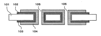
図1は本発明の効果を得るための一例として第1の形態を示す断面模式図となっている。
図1に示すように、シリコン基材もしくはガラス基材101の表裏面に、少なくとも一層以上の無機密着層102が形成され、さらに無機密着層102直上に、下層金属配線層103、上層金属配線層104が積層されており、下層金属配線層103と上層金属配線層104は、その端辺が重ならず、段差を生じており、いわゆる多段構造形状になっている。
これにより、金属配線と前記シリコン基材もしくはガラス基材101との異種材料による線膨張係数による応力差を低減させることで、配線基板の金属配線層周辺のコア材に発生するクラック、割れ、欠けを抑制する構造を得ることができる。
FIG. 1 is a schematic sectional view showing a first embodiment as an example for obtaining the effect of the present invention.
As shown in FIG. 1, at least one or more inorganic
This reduces a stress difference due to a linear expansion coefficient due to a different material between the metal wiring and the silicon base material or the
また、このような構造にすることにより、前記シリコン基材もしくはガラス基材101においてクラックが生じやすい箇所である前記シリコン基材もしくはガラス基材101と前記下層金属配線層103との端部接点が多段構造であることで、材質応力差によるクラックの発生を抑制することができる。かつ、前記上層金属配線層104により金属配線全体の体積が増加することで電気抵抗値を下げることが出来るため、電気特性の劣化を回避することが可能となる。
Further, with such a structure, the end contact between the silicon base material or the
図2に、本発明の第2の形態に係る配線基板の断面を示す。
この配線基板は、脆性材料であるシリコン基材もしくはガラス基材101に、この基材101を貫通する貫通孔105が穿設され、前記シリコン基材もしくはガラス基材101の両面および前記貫通孔内壁上に、無機密着層102が形成されている。そして前記無機密着層102直上に、電気めっきによって下層金属配線層103が形成され、さらに前記下層金属配線層103直上に、電気めっきにより上層金属配線層104が形成されている。
FIG. 2 shows a cross section of a wiring board according to a second embodiment of the present invention.
In this wiring board, a through-
その後、前記下層金属配線層103が形成されていない箇所の前記無機密着層102が除去されることで、図2の構成を得る。なお、図2記載の前記無機密着層102および前記上記金属配線層104の層数および前記下層金属配線103および前記上記上層金属配線104の形状および厚みは、1つの例として図示したものであり、特に規定するものではない。
After that, the
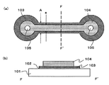
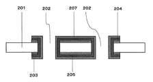
図3〜図5に、本発明の第3〜第5の形態をとる場合のそれぞれの(a)平面図および(b)断面図を示す。 FIGS. 3 to 5 show (a) a plan view and (b) a sectional view, respectively, in the case where the third to fifth embodiments of the present invention are taken.
図3に示すように、本発明の第3の形態においては、下層金属配線層103のパターンが上層金属配線層104のパターンより大きく形成されており、図3(a)平面図では下層金属配線層103のパターンの端部が露出している。中央のFとF’を結ぶ線における(b)断面図では、下層金属配線層103と上層金属配線層104とは、階段状の多段構造になっている。
As shown in FIG. 3, in the third embodiment of the present invention, the pattern of the lower
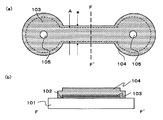
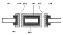
また図4に示すように、本発明の第4の形態においては、下層金属配線層103のパターンは上層金属配線層104のパターンによって完全に覆われて形成されており、図4(a)平面図では下層金属配線層103のパターンは見えなくなっている。中央のFとF’を結ぶ線における(b)断面図では、下層金属配線層103と上層金属配線層104とは、被覆状の多段構造になっている。
Further, as shown in FIG. 4, in the fourth embodiment of the present invention, the pattern of the lower
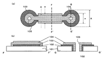
また図5に示すように、本発明の第5の形態においては、図5(a)平面図の中央部分では、下層金属配線層103のパターンは上層金属配線層104のパターンによって完全に覆われて見えなくなっている。一方、図の両端部分ではホールパターンが形成され、ホールの中心には貫通孔105が形成されている。
As shown in FIG. 5, in the fifth embodiment of the present invention, the pattern of the lower
そして、中央のFとF’を結ぶ線における(b)断面図(左側の図)では、下層金属配線層103のパターンは上層金属配線層104のパターンによって覆われており、前記第4の形態と同様な被覆状の多段構造になっている。
一方、右端部のGとG’を結ぶ線における(b)断面図(右側の図)では、基板101上に無機密着層102、下層金属配線層103、上層金属配線層104が順に積層されて、貫通孔105を覆っている。ホールパターンの外周部では、前記第3の形態と同様な階段状の多段構造となっている。
このように、第5の形態においては2種類の多段構造が共存している形となっている。
In the (b) cross-sectional view (left drawing) of the line connecting F and F ′ at the center, the pattern of the lower
On the other hand, in the (b) cross-sectional view (right drawing) of the line connecting G and G ′ at the right end, an inorganic
Thus, in the fifth embodiment, two types of multistage structures coexist.
本発明においては、下層金属配線層103直上に上層金属配線層104が形成されることにより、金属配線層全体の体積が増加することで電気抵抗の低下を図ることができる。また、シリコン基材もしくはガラス基材101と下層金属配線層103および上層金属配線層104が多段構造をとることで、前記シリコン基材もしくはガラス基材101と前記下層金属配線層103の端部接点におけるクラックの抑制が可能となる。
In the present invention, since the upper
<実施例1>
まず、本発明の第3の形態を得るための実施例を、図6〜図13を用いて説明する。
<Example 1>
First, an example for obtaining the third embodiment of the present invention will be described with reference to FIGS.
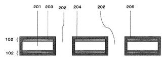
(ガラス基材の形成)
本発明の実施例1として、図6〜図13に示す工程によって配線基板を作製した。厚さ0.3mm、大きさ300×300mm、熱膨張率4ppm/℃のガラスコア基板201に、公知技術であるCO2レーザーにて穴径100μmの貫通孔202を形成し、500℃でアニールすることによって加工歪みを除去した(図6)。
(Formation of glass substrate)
As Example 1 of the present invention, a wiring board was manufactured by the steps shown in FIGS. A through-
(無機密着層の形成)
続いて、図7に示すように、チタン層203を厚さ0.05μm、銅層204を厚さ0.5μmとなるようにスパッタリング処理により形成し、その後、ニッケル層205を厚さ0.2μmとなるように化学めっきによって形成した。
(Formation of inorganic adhesion layer)
Subsequently, as shown in FIG. 7, a
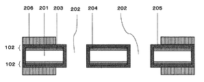
(下層金属配線層の形成)
続いて、厚さ25μmのドライフィルムレジスト206を両面形成後、配線パターンをフォトマスクによって両面パターニング後、1%炭酸ソーダで現像処理することにより、パターニングされたガラスコア基板を得た(図8)。
さらに、下層金属配線層207として電気めっきにて銅層204を2μm形成し(図9)、ドライフィルムレジスト206を剥離後に無機密着層102の除去として、トップリップAZ(奥野製薬)によるニッケル層205の除去、硫酸−過酸化水素からなるエッチング液による銅層204の除去、水酸化カリウム−過酸化水素混合エッチング液によるチタン層203を除去することで、ガラス上に下層金属配線層207を形成された基板を得た(図10)。
(Formation of lower metal wiring layer)
Subsequently, after a dry film resist 206 having a thickness of 25 μm was formed on both sides, the wiring pattern was patterned on both sides with a photomask and then developed with 1% sodium carbonate to obtain a patterned glass core substrate (FIG. 8). .
Further, a
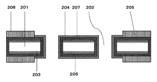
(上層金属配線層の形成)
第3の形態では、図3に示すように、下層金属配線層103の配線パターン部分の寸法
幅を下層金属配線幅Aとし、また上層金属配線層104の配線パターン部分の寸法幅を上層金属配線幅aとする。この場合下層金属配線幅Aに対して、上層金属配線幅aがA>aの形態をとることとなる。下層金属配線層207上にドライフィルムレジスト206を用い、下層金属配線幅aに対して、A>aとなるように、パターニングを行い(図11)、下層金属配線層207直上に電気めっきにて銅4μmの上層金属配線層208を形成した後(図12)、ドライフィルムレジスト206を除去することで本発明の第3の形態における構造が得られた(図13)。
(Formation of upper metal wiring layer)
In the third embodiment, as shown in FIG. 3, the dimensional width of the wiring pattern portion of the lower
なお、図13では上層金属配線層208が一層の事例を示したが、所望の電気抵抗値が得られるよう更に上層金属配線層208を多層化してもよい。
Although FIG. 13 shows an example in which the upper
上記実施例1に示す工程により、図3に示される形状の金属配線パターンが得られた。 The metal wiring pattern having the shape shown in FIG. 3 was obtained by the steps shown in Example 1 above.
<実施例2>
次に、本発明の第4の形態を得るための実施例を示す。
<Example 2>
Next, an example for obtaining the fourth embodiment of the present invention will be described.
(ガラス基材の形成)
本発明の実施例2として、図6〜図10、および図14〜16に示す工程によって配線基板を作製した。厚さ0.3mm、大きさ300×300mm、熱膨張率4ppm/℃のガラスコア基板201に、公知技術であるCO2レーザーにて穴径100μmの貫通孔202を形成し、500℃でアニールすることによって加工歪みを除去した(図6)。
(Formation of glass substrate)
As Example 2 of the present invention, a wiring board was manufactured by the steps shown in FIGS. 6 to 10 and FIGS. A through-
(無機密着層の形成)
続いて、図7に記載するようにチタン層203を厚さ0.05μm、銅層204を厚さ0.5μmとなるようにスパッタリング処理により形成し、その後、ニッケル層205を厚さ0.2μmとなるように化学めっきによって形成した。
(Formation of inorganic adhesion layer)
Subsequently, as shown in FIG. 7, a
(下層金属配線層の形成)
続いて、厚さ25μmのドライフィルムレジスト206を両面形成後、配線パターンをフォトマスクによって両面パターニング後、1%炭酸ソーダで現像処理することにより、パターニングされたガラスコア基板を得た(図8)。さらに、下層金属配線層207として電気めっきにて銅層204を2μm形成し(図9)、ドライフィルムレジスト206を剥離後に無機密着層102の除去として、トップリップAZ(奥野製薬)によるニッケル層205の除去、硫酸−過酸化水素からなるエッチング液による銅層204の除去、水酸化カリウム−過酸化水素混合エッチング液によるチタン層203を除去することで、ガラス上に下層金属配線層207を形成された基板を得た(図10)。
(Formation of lower metal wiring layer)
Subsequently, after a dry film resist 206 having a thickness of 25 μm was formed on both sides, the wiring pattern was patterned on both sides with a photomask and then developed with 1% sodium carbonate to obtain a patterned glass core substrate (FIG. 8). . Further, a
(上層金属配線層の形成)
第4の形態では、図4に示すように下層金属配線幅Aに対して、上層金属配線幅aがA<aの形態をとることとなるため、下層金属配線層207上にドライフィルムレジスト206を用い、下層金属配線幅aに対して、A<aとなるようにパターニングを行い(図14)、下層金属配線層207直上に電気めっきにて銅4μmの上層金属配線層208を形成した後(図15)、ドライフィルムレジスト206を除去することで本発明の第4の形態における構造が得られた(図16)。
(Formation of upper metal wiring layer)
In the fourth embodiment, as shown in FIG. 4, since the upper metal wiring width a has a relation of A <a with respect to the lower metal wiring width A, the dry film resist 206 is formed on the lower
なお、図16では上層金属配線層208が一層の事例を示したが、所望の電気抵抗値が得られるよう更に上層金属配線層を多層化してもよい。
Although FIG. 16 shows an example in which the upper
上記第4の形態の工程により、図4に示される形状の金属配線が得られた。 Through the steps of the fourth embodiment, a metal wiring having the shape shown in FIG. 4 was obtained.
<実施例3>
次に、本発明の第5の形態を得るための実施例を示す。
<Example 3>
Next, an example for obtaining the fifth embodiment of the present invention will be described.
(ガラス基材の形成)
本発明の実施例3として、図6〜図10、および図14〜16に示す工程によって配線基板を作製した。厚さ0.3mm、大きさ300×300mm、熱膨張率4ppm/℃のガラスコア基板201に、公知技術であるCO2レーザーにて穴径100μmの貫通孔202を形成し、500℃でアニールすることによって加工歪みを除去した(図6)。
(Formation of glass substrate)
Example 3 As Example 3 of the present invention, a wiring board was manufactured by the steps shown in FIGS. 6 to 10 and FIGS. A through-
(無機密着層の形成)
続いて、図7に記載するようにチタン層203を厚さ0.05μm、銅層204を厚さ0.5μmとなるようにスパッタリング処理により形成し、その後、ニッケル層205を厚さ0.2μmとなるように化学めっきによって形成した。
(Formation of inorganic adhesion layer)
Subsequently, as shown in FIG. 7, a
(下層金属配線層の形成)
続いて、厚さ25μmのドライフィルムレジスト206を両面形成後、配線パターンをフォトマスクによって両面パターニング後、1%炭酸ソーダで現像処理することにより、パターニングされたガラスコア基板を得た(図8)。さらに、下層金属配線層207として電気めっきにて銅層204を2μm形成し(図9)、ドライフィルムレジスト206を剥離後に無機密着層102の除去として、トップリップAZ(奥野製薬)によるニッケル層205の除去、硫酸−過酸化水素からなるエッチング液による銅層204の除去、水酸化カリウム−過酸化水素混合エッチング液によるチタン層203を除去することで、ガラス上に下層金属配線層207を形成された基板を得た(図10)。
(Formation of lower metal wiring layer)
Subsequently, after a dry film resist 206 having a thickness of 25 μm was formed on both sides, the wiring pattern was patterned on both sides with a photomask and then developed with 1% sodium carbonate to obtain a patterned glass core substrate (FIG. 8). . Further, a
(上層金属配線層の形成)
第5の形態では、図5に示すように下層金属配線幅Aに対して、上層金属配線幅aがA>aかつ一部分がA<aの形態をとることとなるため、下層金属配線層207上にドライフィルムレジスト206を用い、下層金属配線幅aに対して、A<aかつ一部分においては、A>aとなるようにパターニングを行い(図11および図14)、下層金属配線層207直上に電気めっきにて銅4μmの上層金属配線層208を形成した後(図12および図15)、ドライフィルムレジスト206を除去することで本発明の第5の形態における構造が得られる(図13及び図16)。
(Formation of upper metal wiring layer)
In the fifth embodiment, as shown in FIG. 5, the upper metal wiring width a is A> a and a part is A <a with respect to the lower metal wiring width A. Using a dry film resist 206 thereon, patterning is performed so that A <a and, in part, A> a with respect to the lower metal wiring width a (FIGS. 11 and 14). After forming an upper
なお、図13及び図16では上層金属配線層208が一層の事例を示したが、所望の電気抵抗値が得られるよう更に上層金属配線層を多層化してもよい。
Although FIGS. 13 and 16 show an example in which the upper
上記第5の形態の工程により、図5に示される形状の金属配線が得られる。 Through the steps of the fifth embodiment, a metal wiring having the shape shown in FIG. 5 is obtained.
上記実施例1〜3のいずれかの構成を有することで、駆動周波数1GHzにおいて、ガラスコア基板にクラックが生じることがなく、伝送特性低下が生じない基板が得られた。 With the configuration of any one of Examples 1 to 3, at a driving frequency of 1 GHz, a glass core substrate was not cracked, and a substrate with no deterioration in transmission characteristics was obtained.
本発明の配線基板は、ガラスインターポーザ、ガラスコアRFモジュール等に有効である The wiring board of the present invention is effective for a glass interposer, a glass core RF module, and the like.
101 シリコンもしくはガラスからなる基材
102 無機密着層
103 下層金属配線層
104 上層金属配線層
105 貫通孔
A 下層金属配線幅
a 上層金属配線幅
201 ガラスコア基板
202 貫通孔
203 チタン層
204 銅層
205 ニッケル層
206 ドライフィルムレジスト
207 下層金属配線層
208 上層金属配線層
Claims (5)
前記下層金属配線層と上層金属配線層は、それら両層の端辺が重ならない多段構造であることを特徴とする配線基板。 At least one surface on a silicon substrate or a glass substrate has one or more inorganic adhesive layers made of an inorganic compound, and has a lower metal wiring layer made of electroplating on the inorganic adhesive layer. It has an upper metal wiring layer composed of one or more electroplatings on the upper side,
A wiring board, wherein the lower metal wiring layer and the upper metal wiring layer have a multi-stage structure in which the edges of both layers do not overlap.
前記貫通孔の内壁には、前記無機密着層および前記下層金属配線層が積層され、
前記下層金属配線層上に前記上層金属配線層を有することを特徴とする請求項1に記載の配線基板。 The base material has a through hole penetrating the front and back,
On the inner wall of the through hole, the inorganic adhesion layer and the lower metal wiring layer are stacked,
The wiring board according to claim 1, further comprising the upper metal wiring layer on the lower metal wiring layer.
Priority Applications (1)
| Application Number | Priority Date | Filing Date | Title |
|---|---|---|---|
| JP2018122894A JP7279306B2 (en) | 2018-06-28 | 2018-06-28 | wiring board |
Applications Claiming Priority (1)
| Application Number | Priority Date | Filing Date | Title |
|---|---|---|---|
| JP2018122894A JP7279306B2 (en) | 2018-06-28 | 2018-06-28 | wiring board |
Publications (2)
| Publication Number | Publication Date |
|---|---|
| JP2020004845A true JP2020004845A (en) | 2020-01-09 |
| JP7279306B2 JP7279306B2 (en) | 2023-05-23 |
Family
ID=69100590
Family Applications (1)
| Application Number | Title | Priority Date | Filing Date |
|---|---|---|---|
| JP2018122894A Active JP7279306B2 (en) | 2018-06-28 | 2018-06-28 | wiring board |
Country Status (1)
| Country | Link |
|---|---|
| JP (1) | JP7279306B2 (en) |
Cited By (1)
| Publication number | Priority date | Publication date | Assignee | Title |
|---|---|---|---|---|
| JP2022190464A (en) * | 2021-06-14 | 2022-12-26 | 凸版印刷株式会社 | Glass wiring board and manufacturing method of glass wiring board |
Citations (7)
| Publication number | Priority date | Publication date | Assignee | Title |
|---|---|---|---|---|
| JPH0513933A (en) * | 1991-07-02 | 1993-01-22 | Fujitsu Ltd | Printed wiring board conductor pattern and method for forming the same |
| JP2000188447A (en) * | 1998-12-21 | 2000-07-04 | Ibiden Co Ltd | Wiring board and printed wiring board |
| JP2000299540A (en) * | 1999-04-13 | 2000-10-24 | Toshiba Corp | Metallized substrate |
| JP2004349593A (en) * | 2003-05-26 | 2004-12-09 | Sanyo Electric Co Ltd | Semiconductor device and manufacturing method thereof |
| JP2009239184A (en) * | 2008-03-28 | 2009-10-15 | Toppan Printing Co Ltd | Multilayer printed wiring board |
| US20160122180A1 (en) * | 2008-11-19 | 2016-05-05 | Silex Microsystems Ab | Method of making a semiconductor device having a functional capping |
| JP2016154240A (en) * | 2010-03-03 | 2016-08-25 | ジョージア テック リサーチ コーポレイション | Microelectronic package and semiconductor package circuits |
-
2018
- 2018-06-28 JP JP2018122894A patent/JP7279306B2/en active Active
Patent Citations (7)
| Publication number | Priority date | Publication date | Assignee | Title |
|---|---|---|---|---|
| JPH0513933A (en) * | 1991-07-02 | 1993-01-22 | Fujitsu Ltd | Printed wiring board conductor pattern and method for forming the same |
| JP2000188447A (en) * | 1998-12-21 | 2000-07-04 | Ibiden Co Ltd | Wiring board and printed wiring board |
| JP2000299540A (en) * | 1999-04-13 | 2000-10-24 | Toshiba Corp | Metallized substrate |
| JP2004349593A (en) * | 2003-05-26 | 2004-12-09 | Sanyo Electric Co Ltd | Semiconductor device and manufacturing method thereof |
| JP2009239184A (en) * | 2008-03-28 | 2009-10-15 | Toppan Printing Co Ltd | Multilayer printed wiring board |
| US20160122180A1 (en) * | 2008-11-19 | 2016-05-05 | Silex Microsystems Ab | Method of making a semiconductor device having a functional capping |
| JP2016154240A (en) * | 2010-03-03 | 2016-08-25 | ジョージア テック リサーチ コーポレイション | Microelectronic package and semiconductor package circuits |
Cited By (1)
| Publication number | Priority date | Publication date | Assignee | Title |
|---|---|---|---|---|
| JP2022190464A (en) * | 2021-06-14 | 2022-12-26 | 凸版印刷株式会社 | Glass wiring board and manufacturing method of glass wiring board |
Also Published As
| Publication number | Publication date |
|---|---|
| JP7279306B2 (en) | 2023-05-23 |
Similar Documents
| Publication | Publication Date | Title |
|---|---|---|
| US8387239B2 (en) | Manufacturing method of embedded circuit substrate | |
| US9370102B2 (en) | Embedded multilayer ceramic electronic component and printed circuit board having embedded multilayer ceramic electronic component | |
| JP2002016183A (en) | Circuit board for semiconductor package and method of manufacturing the same | |
| CN111328427A (en) | Wiring board, semiconductor device, and manufacturing method of wiring board | |
| US20170033037A1 (en) | Packaging substrate | |
| JPWO2011007659A1 (en) | Signal line and manufacturing method thereof | |
| US9338887B2 (en) | Core substrate, manufacturing method thereof, and structure for metal via | |
| WO2012124421A1 (en) | Flexible multilayer substrate | |
| JP4525786B2 (en) | Electronic components and electronic component modules | |
| JP2012234857A (en) | Ceramic circuit boad and module using the same | |
| CN114026967A (en) | Method for manufacturing ceramic substrate | |
| JP2001251024A (en) | Method of manufacturing multilayer assembly board and multilayer ceramic component | |
| US11864316B2 (en) | Wiring substrate | |
| JP2020004845A (en) | Wiring board | |
| JP2017005232A (en) | Electronic component built-in wiring board | |
| CN1351815A (en) | Flexible printed wiring board and its production method | |
| TW201220964A (en) | Carrier board | |
| TW202110297A (en) | Substrate structure and manufacturing method thereof | |
| WO2024062808A1 (en) | Wiring substrate | |
| TWI715458B (en) | Method for manufacturing rigid printed circuit board | |
| TWI501706B (en) | Circuit board and manufacturing method thereof | |
| WO2012164719A1 (en) | Substrate with built-in component, and method for producing said substrate | |
| US8383953B2 (en) | Circuit board and method for manufacturing the same | |
| JP2003332503A (en) | Circuit board having heat sink and manufacturing method thereof | |
| JPWO2017077837A1 (en) | Component mounting board |
Legal Events
| Date | Code | Title | Description |
|---|---|---|---|
| A621 | Written request for application examination |
Free format text: JAPANESE INTERMEDIATE CODE: A621 Effective date: 20210519 |
|
| A977 | Report on retrieval |
Free format text: JAPANESE INTERMEDIATE CODE: A971007 Effective date: 20220221 |
|
| A131 | Notification of reasons for refusal |
Free format text: JAPANESE INTERMEDIATE CODE: A131 Effective date: 20220329 |
|
| A521 | Request for written amendment filed |
Free format text: JAPANESE INTERMEDIATE CODE: A523 Effective date: 20220525 |
|
| A131 | Notification of reasons for refusal |
Free format text: JAPANESE INTERMEDIATE CODE: A131 Effective date: 20221018 |
|
| A521 | Request for written amendment filed |
Free format text: JAPANESE INTERMEDIATE CODE: A523 Effective date: 20221207 |
|
| TRDD | Decision of grant or rejection written | ||
| A01 | Written decision to grant a patent or to grant a registration (utility model) |
Free format text: JAPANESE INTERMEDIATE CODE: A01 Effective date: 20230411 |
|
| A61 | First payment of annual fees (during grant procedure) |
Free format text: JAPANESE INTERMEDIATE CODE: A61 Effective date: 20230424 |
|
| R150 | Certificate of patent or registration of utility model |
Ref document number: 7279306 Country of ref document: JP Free format text: JAPANESE INTERMEDIATE CODE: R150 |
|
| R250 | Receipt of annual fees |
Free format text: JAPANESE INTERMEDIATE CODE: R250 |