JP3853373B2 - 電気回路及び制御装置 - Google Patents
電気回路及び制御装置 Download PDFInfo
- Publication number
- JP3853373B2 JP3853373B2 JP52305198A JP52305198A JP3853373B2 JP 3853373 B2 JP3853373 B2 JP 3853373B2 JP 52305198 A JP52305198 A JP 52305198A JP 52305198 A JP52305198 A JP 52305198A JP 3853373 B2 JP3853373 B2 JP 3853373B2
- Authority
- JP
- Japan
- Prior art keywords
- control device
- circuit board
- casing
- connector
- plug
- Prior art date
- Legal status (The legal status is an assumption and is not a legal conclusion. Google has not performed a legal analysis and makes no representation as to the accuracy of the status listed.)
- Expired - Fee Related
Links
Images

Classifications
-
- B—PERFORMING OPERATIONS; TRANSPORTING
- B60—VEHICLES IN GENERAL
- B60R—VEHICLES, VEHICLE FITTINGS, OR VEHICLE PARTS, NOT OTHERWISE PROVIDED FOR
- B60R16/00—Electric or fluid circuits specially adapted for vehicles and not otherwise provided for; Arrangement of elements of electric or fluid circuits specially adapted for vehicles and not otherwise provided for
- B60R16/02—Electric or fluid circuits specially adapted for vehicles and not otherwise provided for; Arrangement of elements of electric or fluid circuits specially adapted for vehicles and not otherwise provided for electric constitutive elements
- B60R16/023—Electric or fluid circuits specially adapted for vehicles and not otherwise provided for; Arrangement of elements of electric or fluid circuits specially adapted for vehicles and not otherwise provided for electric constitutive elements for transmission of signals between vehicle parts or subsystems
- B60R16/0239—Electronic boxes
-
- H—ELECTRICITY
- H01—ELECTRIC ELEMENTS
- H01R—ELECTRICALLY-CONDUCTIVE CONNECTIONS; STRUCTURAL ASSOCIATIONS OF A PLURALITY OF MUTUALLY-INSULATED ELECTRICAL CONNECTING ELEMENTS; COUPLING DEVICES; CURRENT COLLECTORS
- H01R13/00—Details of coupling devices of the kinds covered by groups H01R12/70 or H01R24/00 - H01R33/00
- H01R13/02—Contact members
- H01R13/04—Pins or blades for co-operation with sockets
-
- H—ELECTRICITY
- H01—ELECTRIC ELEMENTS
- H01R—ELECTRICALLY-CONDUCTIVE CONNECTIONS; STRUCTURAL ASSOCIATIONS OF A PLURALITY OF MUTUALLY-INSULATED ELECTRICAL CONNECTING ELEMENTS; COUPLING DEVICES; CURRENT COLLECTORS
- H01R12/00—Structural associations of a plurality of mutually-insulated electrical connecting elements, specially adapted for printed circuits, e.g. printed circuit boards [PCB], flat or ribbon cables, or like generally planar structures, e.g. terminal strips, terminal blocks; Coupling devices specially adapted for printed circuits, flat or ribbon cables, or like generally planar structures; Terminals specially adapted for contact with, or insertion into, printed circuits, flat or ribbon cables, or like generally planar structures
- H01R12/70—Coupling devices
-
- H—ELECTRICITY
- H01—ELECTRIC ELEMENTS
- H01R—ELECTRICALLY-CONDUCTIVE CONNECTIONS; STRUCTURAL ASSOCIATIONS OF A PLURALITY OF MUTUALLY-INSULATED ELECTRICAL CONNECTING ELEMENTS; COUPLING DEVICES; CURRENT COLLECTORS
- H01R12/00—Structural associations of a plurality of mutually-insulated electrical connecting elements, specially adapted for printed circuits, e.g. printed circuit boards [PCB], flat or ribbon cables, or like generally planar structures, e.g. terminal strips, terminal blocks; Coupling devices specially adapted for printed circuits, flat or ribbon cables, or like generally planar structures; Terminals specially adapted for contact with, or insertion into, printed circuits, flat or ribbon cables, or like generally planar structures
- H01R12/70—Coupling devices
- H01R12/7094—Coupling devices with switch operated by engagement of PCB
-
- H—ELECTRICITY
- H01—ELECTRIC ELEMENTS
- H01R—ELECTRICALLY-CONDUCTIVE CONNECTIONS; STRUCTURAL ASSOCIATIONS OF A PLURALITY OF MUTUALLY-INSULATED ELECTRICAL CONNECTING ELEMENTS; COUPLING DEVICES; CURRENT COLLECTORS
- H01R13/00—Details of coupling devices of the kinds covered by groups H01R12/70 or H01R24/00 - H01R33/00
- H01R13/648—Protective earth or shield arrangements on coupling devices, e.g. anti-static shielding
- H01R13/658—High frequency shielding arrangements, e.g. against EMI [Electro-Magnetic Interference] or EMP [Electro-Magnetic Pulse]
- H01R13/6598—Shield material
- H01R13/6599—Dielectric material made conductive, e.g. plastic material coated with metal
-
- H—ELECTRICITY
- H05—ELECTRIC TECHNIQUES NOT OTHERWISE PROVIDED FOR
- H05K—PRINTED CIRCUITS; CASINGS OR CONSTRUCTIONAL DETAILS OF ELECTRIC APPARATUS; MANUFACTURE OF ASSEMBLAGES OF ELECTRICAL COMPONENTS
- H05K5/00—Casings, cabinets or drawers for electric apparatus
- H05K5/0026—Casings, cabinets or drawers for electric apparatus provided with connectors and printed circuit boards [PCB], e.g. automotive electronic control units
- H05K5/0069—Casings, cabinets or drawers for electric apparatus provided with connectors and printed circuit boards [PCB], e.g. automotive electronic control units having connector relating features for connecting the connector pins with the PCB or for mounting the connector body with the housing
Landscapes
- Engineering & Computer Science (AREA)
- Microelectronics & Electronic Packaging (AREA)
- Mechanical Engineering (AREA)
- Shielding Devices Or Components To Electric Or Magnetic Fields (AREA)
- Details Of Connecting Devices For Male And Female Coupling (AREA)
- Coupling Device And Connection With Printed Circuit (AREA)
- Electrical Discharge Machining, Electrochemical Machining, And Combined Machining (AREA)
- Selective Calling Equipment (AREA)
- Steering Control In Accordance With Driving Conditions (AREA)
Description
本発明は、請求の範囲第1項の上位概念による電気回路及び制御装置に関する。このような回路及び制御装置はドイツ連邦共和国特許出願公開第3310477号公報から公知である。
この公知の回路及び制御装置では、金属ピンがコネクタボデーに設けられ、機械的に保護されたマルチポイントコネクタを形成している。しかしこのマルチポイントコネクタは電気的および電磁気的影響に対する保護機能を有していない。またこのマルチポイントコネクタは、周囲の環境を、この回路及び制御装置からの電磁波放射によって発生する影響から保護することもできない。
本発明の課題は、上記の欠点を回避した、電気回路及び制御装置を提供することである。本発明による装置は、外部の電気的または電磁的影響から保護されると同時に、この回路及び制御装置の周囲の環境を、この回路及び制御装置自身を発生源とする電磁波から保護する。これに加えて、回路支持体としてのプリント配線回路板とコネクタプラグとの間、または対向するコネクタを介してこのコネクタプラグに接続されたケーブルとの間に信頼性が高く、かつ自由に形成可能な接続が得られるようにすることである。
上記の課題は、本発明により請求の範囲第1項の特徴とする構成によって解決される。請求の範囲第1項の装置の有利な実施形態は、従属請求項の以下の説明および図面に記載されている。
図面
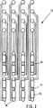
本発明の実施例を図に示し、以下詳しく説明する。ここで、図1は、回路及び制御装置の一部の断面図を示し、図2は制御装置の金属の構造層の平面図を示している。
実施例の説明
詳細には図示していない回路及び制御装置1は、複数のケーシング被覆部を備えたプラスティック製のケーシング2を有している。図1ではこのようなケーシング被覆部の2つ、すなわち側面のケーシング被覆部3と下方のケーシング被覆部4とが示されている。
側面のケーシング被覆部3は、少なくとも2つの側方張出し部5と6と共に多数のピン8が設けられているプラグ7の凹入部を覆っている。これらのピンがいわゆるポイントコネクタ端子9を形成している。プラグ7は、マルチポイントコネクタ端子9と共に、図示されていないケーブルコネクタソケットと接続される。プラグ7の内側面、すなわち張出し部5と6の内側面10、およびプラグ7の底面11には、金属層12が設けられている。この層は、電磁波(入射および出射)をシールドするためのものである。マルチポイントコネクタ端子9はリフローはんだ付けプロセスにおいて処理可能である。
ピン8は、ケーシング被覆部3を貫通し、内側において、つまりケーシング2の内側で、金属構造層13に埋め込まれている。ケーシング2のこの内側面は、レイアウト面とも称され、図2に示されている。層13はモールドプリント回路部品(Molded Interconnected Devices)技術で製造される。
この技術では、耐熱性のプラスティックが使用される。このプラスティック材はプラスティック放出法で製作され、また導電材の安定した付着を保証する。この技術で製造される部分は、標準の電子製造において処理可能であり、したがってはんだ付けは、リフロー炉でも、はんだウェーブで行ってもよい。
図2で示した、斑点の存在する円はアースに対する貫通接触接続点14である。白い長方形は、例えばコンデンサ15のような電気部品または電子構成部品を示している。白い円は、プリント配線回路板17の回路支持面18上への貫通接触接続点16である。この回路面側18は図1に示されている。貫通接触接続点14と16は、信号をさらに先へと導くために使用されている。プリント配線回路板17の代わりに、シートまたはサブストレートを使用することもできる。
ケーシング2にプリント配線回路板17を固定し、その接触接続のために、金属被膜が形成されたプラスティック支柱19が設けられている。この支柱がはんだ付け位置を形成する。この支柱19は、種々の方法、例えば接着、ボンディング、またはリフローはんだ付けでプリント配線回路板17に接続することができる。実施例ではBGA(Ball Grid Array)技法により、リフローはんだ付け法にてはんだ付けされている。
BGA技術は、特に数多くの接続端子を有する構成素子において使用される。接続端子は、構成素子のボデーに垂直に立っているピン8をそれぞれ有している。このピンの自由端には、球状のはんだが取り付けられている。ピン8はプリント配線回路板17の接続パッド当接されており、はんだが溶融することによって、ピン8とそれに対応する接続パッドとの電気接続が行われる。
作用および機能
ケーシング2の内部に設けられた層13は、回路及び制御装置1を、電気的および/または電磁気的な種類の外部からの影響から保護するために使用される。またこの他にケーシング2は、機械的な保護の働きをしている。
マルチポイントコネクタ端子9の領域に層12が設けられたプラグ7は、回路及び制御装置の周囲を電磁波をシールドするという働きをしている。
貫通接触接続点14および16により、カレントパススルーとも称される、所要の電気的クロスコネクション、例えばピン8とプリント配線回路板17の任意の点との間の接続は容易に実現される。
また必要に応じて例えばコンデンサのような、別の電子構成素子をマルチポイントコネクタ端子上に装着可能である。
Claims (2)
- ケーシング(2)を備えた、自動車用の電気回路及び制御装置であって、
前記ケーシングは、1つの面に、電気的なコネクタ接続を形成するための対向コネクタ収容部を備えたプラグ(7)と、前記ケーシング(2)に対して設けられたプリント配線回路板(17)とを有し、
前記コネクタ(7)は、マルチポイントコネクタ端子(9)を形成する、相互に絶縁された多数の金属ピンを有し、
プラグ接続を行う際には、対向するコネクタの対向接触接続要素は、前記マルチポイントコネクタ端子と電気的に接続され、
前記プリント配線回路板には、電気的構成素子と導体路が設けられており、
前記プリント配線回路板は、前記プラグ(7)と接続している回路及び制御装置において、
前記プラグ(7)には、対向コネクタを収容するために設けられた側の内側面(10)と、底面(11)とに層(12)が設けられ、
該層は、電磁波をシールドし、
ケーシング被覆部(3)の、前記マルチポイントコネクタ端子(9)とは反対側に金属の構造層(13)が設けられており、
前記金属の構造層(13)は、一方では貫通接触接続点(14)を介して前記マルチポイントコネクタ端子(9)のピン(8)と接触接続され、他方では貫通接触接続点(16)を介して前記プリント配線回路板(17)と接続されて、前記回路及び制御装置(1)を、電気的または電磁気的な外部の影響を受けないようにシールドし、
前記ケーシング(2)の、前記プリント配線回路板側の壁面に、プラスティックの支柱(19)が設けられており、
該支柱に、前記プリント配線回路板(17)に通じる貫通接触接続点(16)が設けられていることを特徴とする回路及び制御装置。 - 前記金属の構造層(13)上に、電子的構成素子例えばコンデンサ(15)が配置されている、
請求の範囲第1項に記載の回路及び制御装置。
Applications Claiming Priority (3)
| Application Number | Priority Date | Filing Date | Title |
|---|---|---|---|
| DE29619867U DE29619867U1 (de) | 1996-11-15 | 1996-11-15 | Elektrisches Schalt- und Steuergerät |
| DE29619867.6 | 1996-11-15 | ||
| PCT/DE1997/001379 WO1998022993A1 (de) | 1996-11-15 | 1997-07-02 | Elektrisches schalt- und steuergerät |
Publications (2)
| Publication Number | Publication Date |
|---|---|
| JP2000503470A JP2000503470A (ja) | 2000-03-21 |
| JP3853373B2 true JP3853373B2 (ja) | 2006-12-06 |
Family
ID=8031982
Family Applications (1)
| Application Number | Title | Priority Date | Filing Date |
|---|---|---|---|
| JP52305198A Expired - Fee Related JP3853373B2 (ja) | 1996-11-15 | 1997-07-02 | 電気回路及び制御装置 |
Country Status (7)
| Country | Link |
|---|---|
| EP (1) | EP0892999B1 (ja) |
| JP (1) | JP3853373B2 (ja) |
| KR (1) | KR100537300B1 (ja) |
| CN (1) | CN1118902C (ja) |
| DE (2) | DE29619867U1 (ja) |
| RU (1) | RU2185014C2 (ja) |
| WO (1) | WO1998022993A1 (ja) |
Families Citing this family (6)
| Publication number | Priority date | Publication date | Assignee | Title |
|---|---|---|---|---|
| DE102007044359A1 (de) | 2007-09-17 | 2009-03-19 | Robert Bosch Gmbh | LDS Stecker |
| DE102008022973B4 (de) | 2008-05-09 | 2015-08-06 | Hella Kgaa Hueck & Co. | Elektrische Verbindung mit mindestens zwei Bauteilen |
| RU2476964C2 (ru) * | 2011-05-27 | 2013-02-27 | Евгений Владиславович Чёрный | Способ соединения печатной платы с несущей конструкцией |
| DE102011082140B4 (de) * | 2011-09-05 | 2024-09-19 | Kiekert Aktiengesellschaft | Schloss für ein Kraftfahrzeug |
| DE102014200975B4 (de) | 2014-01-21 | 2026-03-19 | Robert Bosch Gmbh | Anordnung aus Leiterplatte, Kontaktstift und elektrisch leitfähigem Klebstoff sowie Verfahren zum Herstellen einer solchen |
| CN110401578A (zh) * | 2019-06-15 | 2019-11-01 | 江苏华兮网络科技工程有限公司 | 一种用于检测网络设备网速的检测设备 |
Family Cites Families (6)
| Publication number | Priority date | Publication date | Assignee | Title |
|---|---|---|---|---|
| JPS57168540A (en) * | 1981-04-10 | 1982-10-16 | Nissan Motor Co Ltd | Noise preventing device and its production for electronic controller |
| DE3310477A1 (de) * | 1982-07-17 | 1984-01-19 | Robert Bosch Gmbh, 7000 Stuttgart | Elektrisches geraet, insbesondere schalt- und steuergeraet fuer kraftfahrzeuge |
| DE3345701A1 (de) * | 1983-12-17 | 1985-06-27 | Robert Bosch Gmbh, 7000 Stuttgart | Elektrisches schaltgeraet mit einer steckerteile tragenden, stirnseitigen anschlussplatte |
| EP0563071B1 (de) * | 1990-12-21 | 1995-03-01 | Siemens Aktiengesellschaft | Gegen hf abschirmendes gehaüse einer schaltung, z.b. für die steuerschaltung eines airbag eines fahrzeuges |
| JPH0521110A (ja) * | 1991-07-10 | 1993-01-29 | Amp Japan Ltd | シールド型電気コネクタ |
| DE4142138C2 (de) * | 1991-12-20 | 1998-04-23 | Bosch Gmbh Robert | Elektrisches Steuergerät |
-
1996
- 1996-11-15 DE DE29619867U patent/DE29619867U1/de not_active Expired - Lifetime
-
1997
- 1997-07-02 RU RU98115278/09A patent/RU2185014C2/ru not_active IP Right Cessation
- 1997-07-02 KR KR1019980705366A patent/KR100537300B1/ko not_active Expired - Fee Related
- 1997-07-02 CN CN97191630A patent/CN1118902C/zh not_active Expired - Fee Related
- 1997-07-02 JP JP52305198A patent/JP3853373B2/ja not_active Expired - Fee Related
- 1997-07-02 DE DE59712659T patent/DE59712659D1/de not_active Expired - Fee Related
- 1997-07-02 WO PCT/DE1997/001379 patent/WO1998022993A1/de not_active Ceased
- 1997-07-02 EP EP97931697A patent/EP0892999B1/de not_active Expired - Lifetime
Also Published As
| Publication number | Publication date |
|---|---|
| CN1118902C (zh) | 2003-08-20 |
| KR19990077224A (ko) | 1999-10-25 |
| EP0892999B1 (de) | 2006-05-24 |
| DE59712659D1 (de) | 2006-06-29 |
| CN1207213A (zh) | 1999-02-03 |
| KR100537300B1 (ko) | 2006-03-16 |
| EP0892999A1 (de) | 1999-01-27 |
| JP2000503470A (ja) | 2000-03-21 |
| RU2185014C2 (ru) | 2002-07-10 |
| DE29619867U1 (de) | 1998-03-12 |
| WO1998022993A1 (de) | 1998-05-28 |
Similar Documents
| Publication | Publication Date | Title |
|---|---|---|
| US7090502B2 (en) | Board connecting component and three-dimensional connecting structure using thereof | |
| US6344682B1 (en) | Semiconductor device comprising a semiconductor element mounted on a substrate and covered by a wiring board | |
| JPH0676894A (ja) | コネクタ | |
| WO1999013571A1 (en) | Shielded surface acoustical wave package | |
| JP3826054B2 (ja) | 基板側コネクタとシールドケーブル側コネクタとの接続構造 | |
| JP2008226786A (ja) | 電子機器 | |
| KR100537300B1 (ko) | 전기 스위칭 및 제어장치 | |
| FI116265B (fi) | Painettu piirilevy | |
| US20020054485A1 (en) | Apparatus for shielding | |
| JP4031549B2 (ja) | 端子のシールド構造 | |
| JP3019373B2 (ja) | コネクタ装置 | |
| JP2822984B2 (ja) | 混成集積回路のシールド構造 | |
| JP2785502B2 (ja) | プリント基板 | |
| JP3019372B2 (ja) | コネクタ装置 | |
| JP3497680B2 (ja) | 半導体パッケージを有する回路モジュールおよび回路モジュールを搭載した電子機器 | |
| JP2827950B2 (ja) | 混成集積回路装置 | |
| JP2003092458A (ja) | フレキシブルプリント基板及びそのチェック方法 | |
| WO2025084094A1 (ja) | 電気機器 | |
| JPH0558260B2 (ja) | ||
| JPH0479352A (ja) | 半導体装置 | |
| JPH0220758Y2 (ja) | ||
| JP2019507480A (ja) | プリント回路基板用のシールド接続要素 | |
| JP3158773B2 (ja) | 回路ユニットの製造方法 | |
| JPH042478Y2 (ja) | ||
| JPH02163958A (ja) | 半導体装置 |
Legal Events
| Date | Code | Title | Description |
|---|---|---|---|
| A621 | Written request for application examination |
Free format text: JAPANESE INTERMEDIATE CODE: A621 Effective date: 20040701 |
|
| A131 | Notification of reasons for refusal |
Free format text: JAPANESE INTERMEDIATE CODE: A131 Effective date: 20051220 |
|
| A601 | Written request for extension of time |
Free format text: JAPANESE INTERMEDIATE CODE: A601 Effective date: 20060317 |
|
| A602 | Written permission of extension of time |
Free format text: JAPANESE INTERMEDIATE CODE: A602 Effective date: 20060508 |
|
| A521 | Request for written amendment filed |
Free format text: JAPANESE INTERMEDIATE CODE: A523 Effective date: 20060620 |
|
| TRDD | Decision of grant or rejection written | ||
| A01 | Written decision to grant a patent or to grant a registration (utility model) |
Free format text: JAPANESE INTERMEDIATE CODE: A01 Effective date: 20060808 |
|
| A61 | First payment of annual fees (during grant procedure) |
Free format text: JAPANESE INTERMEDIATE CODE: A61 Effective date: 20060906 |
|
| R150 | Certificate of patent or registration of utility model |
Free format text: JAPANESE INTERMEDIATE CODE: R150 |
|
| FPAY | Renewal fee payment (event date is renewal date of database) |
Free format text: PAYMENT UNTIL: 20100915 Year of fee payment: 4 |
|
| LAPS | Cancellation because of no payment of annual fees |