JP4366193B2 - スタンパ原盤の製造方法及びスタンパの製造方法 - Google Patents
スタンパ原盤の製造方法及びスタンパの製造方法 Download PDFInfo
- Publication number
- JP4366193B2 JP4366193B2 JP2003585081A JP2003585081A JP4366193B2 JP 4366193 B2 JP4366193 B2 JP 4366193B2 JP 2003585081 A JP2003585081 A JP 2003585081A JP 2003585081 A JP2003585081 A JP 2003585081A JP 4366193 B2 JP4366193 B2 JP 4366193B2
- Authority
- JP
- Japan
- Prior art keywords
- resist layer
- stamper
- crosslinked
- resist
- light
- Prior art date
- Legal status (The legal status is an assumption and is not a legal conclusion. Google has not performed a legal analysis and makes no representation as to the accuracy of the status listed.)
- Expired - Fee Related
Links
Images





Classifications
-
- G—PHYSICS
- G03—PHOTOGRAPHY; CINEMATOGRAPHY; ANALOGOUS TECHNIQUES USING WAVES OTHER THAN OPTICAL WAVES; ELECTROGRAPHY; HOLOGRAPHY
- G03F—PHOTOMECHANICAL PRODUCTION OF TEXTURED OR PATTERNED SURFACES, e.g. FOR PRINTING, FOR PROCESSING OF SEMICONDUCTOR DEVICES; MATERIALS THEREFOR; ORIGINALS THEREFOR; APPARATUS SPECIALLY ADAPTED THEREFOR
- G03F7/00—Photomechanical, e.g. photolithographic, production of textured or patterned surfaces, e.g. printing surfaces; Materials therefor, e.g. comprising photoresists; Apparatus specially adapted therefor
- G03F7/0002—Lithographic processes using patterning methods other than those involving the exposure to radiation, e.g. by stamping
-
- B—PERFORMING OPERATIONS; TRANSPORTING
- B82—NANOTECHNOLOGY
- B82Y—SPECIFIC USES OR APPLICATIONS OF NANOSTRUCTURES; MEASUREMENT OR ANALYSIS OF NANOSTRUCTURES; MANUFACTURE OR TREATMENT OF NANOSTRUCTURES
- B82Y10/00—Nanotechnology for information processing, storage or transmission, e.g. quantum computing or single electron logic
-
- B—PERFORMING OPERATIONS; TRANSPORTING
- B82—NANOTECHNOLOGY
- B82Y—SPECIFIC USES OR APPLICATIONS OF NANOSTRUCTURES; MEASUREMENT OR ANALYSIS OF NANOSTRUCTURES; MANUFACTURE OR TREATMENT OF NANOSTRUCTURES
- B82Y40/00—Manufacture or treatment of nanostructures
-
- G—PHYSICS
- G03—PHOTOGRAPHY; CINEMATOGRAPHY; ANALOGOUS TECHNIQUES USING WAVES OTHER THAN OPTICAL WAVES; ELECTROGRAPHY; HOLOGRAPHY
- G03F—PHOTOMECHANICAL PRODUCTION OF TEXTURED OR PATTERNED SURFACES, e.g. FOR PRINTING, FOR PROCESSING OF SEMICONDUCTOR DEVICES; MATERIALS THEREFOR; ORIGINALS THEREFOR; APPARATUS SPECIALLY ADAPTED THEREFOR
- G03F7/00—Photomechanical, e.g. photolithographic, production of textured or patterned surfaces, e.g. printing surfaces; Materials therefor, e.g. comprising photoresists; Apparatus specially adapted therefor
- G03F7/0017—Photomechanical, e.g. photolithographic, production of textured or patterned surfaces, e.g. printing surfaces; Materials therefor, e.g. comprising photoresists; Apparatus specially adapted therefor for the production of embossing, cutting or similar devices; for the production of casting means
-
- G—PHYSICS
- G03—PHOTOGRAPHY; CINEMATOGRAPHY; ANALOGOUS TECHNIQUES USING WAVES OTHER THAN OPTICAL WAVES; ELECTROGRAPHY; HOLOGRAPHY
- G03F—PHOTOMECHANICAL PRODUCTION OF TEXTURED OR PATTERNED SURFACES, e.g. FOR PRINTING, FOR PROCESSING OF SEMICONDUCTOR DEVICES; MATERIALS THEREFOR; ORIGINALS THEREFOR; APPARATUS SPECIALLY ADAPTED THEREFOR
- G03F7/00—Photomechanical, e.g. photolithographic, production of textured or patterned surfaces, e.g. printing surfaces; Materials therefor, e.g. comprising photoresists; Apparatus specially adapted therefor
- G03F7/004—Photosensitive materials
- G03F7/0045—Photosensitive materials with organic non-macromolecular light-sensitive compounds not otherwise provided for, e.g. dissolution inhibitors
-
- G—PHYSICS
- G11—INFORMATION STORAGE
- G11B—INFORMATION STORAGE BASED ON RELATIVE MOVEMENT BETWEEN RECORD CARRIER AND TRANSDUCER
- G11B7/00—Recording or reproducing by optical means, e.g. recording using a thermal beam of optical radiation by modifying optical properties or the physical structure, reproducing using an optical beam at lower power by sensing optical properties; Record carriers therefor
- G11B7/24—Record carriers characterised by shape, structure or physical properties, or by the selection of the material
- G11B7/26—Apparatus or processes specially adapted for the manufacture of record carriers
- G11B7/261—Preparing a master, e.g. exposing photoresist, electroforming
-
- G—PHYSICS
- G11—INFORMATION STORAGE
- G11B—INFORMATION STORAGE BASED ON RELATIVE MOVEMENT BETWEEN RECORD CARRIER AND TRANSDUCER
- G11B7/00—Recording or reproducing by optical means, e.g. recording using a thermal beam of optical radiation by modifying optical properties or the physical structure, reproducing using an optical beam at lower power by sensing optical properties; Record carriers therefor
- G11B7/24—Record carriers characterised by shape, structure or physical properties, or by the selection of the material
- G11B7/26—Apparatus or processes specially adapted for the manufacture of record carriers
- G11B7/263—Preparing and using a stamper, e.g. pressing or injection molding substrates
Landscapes
- Engineering & Computer Science (AREA)
- Physics & Mathematics (AREA)
- Chemical & Material Sciences (AREA)
- Nanotechnology (AREA)
- General Physics & Mathematics (AREA)
- Manufacturing & Machinery (AREA)
- Crystallography & Structural Chemistry (AREA)
- Condensed Matter Physics & Semiconductors (AREA)
- Mathematical Physics (AREA)
- Theoretical Computer Science (AREA)
- Spectroscopy & Molecular Physics (AREA)
- Manufacturing Optical Record Carriers (AREA)
- Moulds For Moulding Plastics Or The Like (AREA)
Description
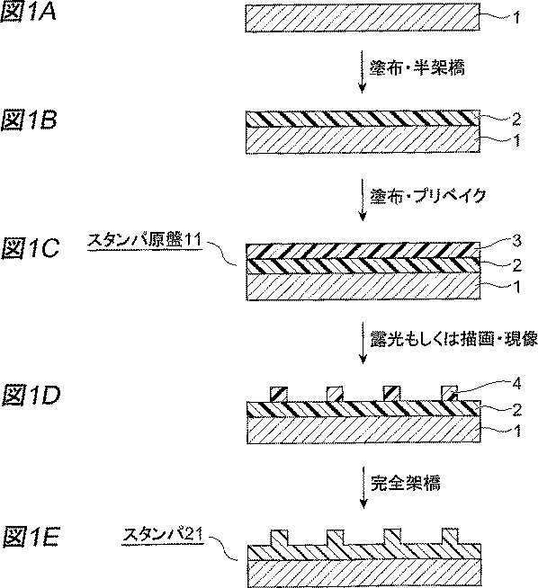
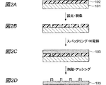
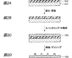
図2A〜Dは、従来のスタンパの製造方法を模式的に示す工程図である。
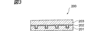
図3は、光ディスクの一実施形態を示す断面図である。
<スタンパ原盤の製造>
まず、外径200mm、厚さ0.3mmであるNi基盤の一方の面を酸化セリウム(CeO2)を用いて機械研磨した。次に、Ni基盤の研磨された面に下記式(1)で表される化合物を含有するアルカリ可溶性ネガ型レジスト(NNR600S2、ナガセケムテックス株式会社製)を、スピンコーターによって200nmの厚さに塗布した。
<スタンパの製造>
得られたスタンパ原盤のプリベイクレジスト層にArレーザー(351nm)を所定のパターンで照射して一定の情報を記録した後、110℃に設定されたホットプレート内で4分間のベーキングを行った。次いで、1.57wt%のTMAH水溶液を用いて、常温(約24℃)で60秒間のスピン現像を行い、露光部を除去してレジストバンプを形成した。次いで、レジストバンプが形成されたスタンパ原盤に対し、175℃に設定されたホットプレート内で10分間処理した後に250℃に設定されたホットプレート内で10分間の処理を行う多段ベークを施した。さらに、ディープUV光を用いて半架橋レジスト層及びレジストバンプを完全架橋した。それから、そのスタンパ原盤を外径138mm、内径22mmのドーナツ状に打ち抜き、スタンパを製造した。
<光ディスクの製造>
光ディスク基盤の材料として、ポリカーボネート樹脂を用いた。上述の実施例2で得たスタンパを金型に取り付け、射出圧縮成形によって、そのスタンパに記録された情報パターンが転写された外径120mm、内径15mmの光ディスク基盤を得た。次に、その光ディスク基盤における情報パターン転写面にアルミニウムスパッタリングを施して反射膜を成膜した。さらに、その反射膜上に光ディスク基盤と同じ大きさのポリカーボネート製ダミー盤を接着剤を用いて貼り合わせ、光ディスクを製造した。
Claims (3)
- 基盤上に熱及び/又は光線によって架橋反応を生じる化合物を塗布し、加熱又は光線を照射することにより前記化合物が完全に架橋しない程度に架橋反応を生じさせて半架橋レジスト層を形成する工程と、
前記半架橋レジスト層上に、下記式(1)で表される化合物を含有して成るプリベイクレジスト層を形成する工程と、を備え、
前記プリベイクレジスト層を形成する工程において、プリベイクは85〜95℃で加熱することで行う、スタンパ原盤の製造方法。
- 前記プリベイクレジスト層を形成する工程を実施した後に該プリベイクレジスト層上に保護膜を形成する工程を備える請求項1に記載のスタンパ原盤の製造方法。
- 基盤上に熱及び/又は光線によって架橋反応を生じる化合物を塗布し、加熱又は光線を照射することにより前記化合物が完全に架橋しない程度に架橋反応を生じさせて半架橋レジスト層を形成する工程と、
前記半架橋レジスト層上に、下記式(1)で表される化合物を含有して成るプリベイクレジスト層を85〜95℃で加熱することで形成する工程と、
該プリベイクレジスト層に一定の情報を記録する工程と、
情報が記録された前記プリベイクレジスト層を現像してバンプを形成する工程と、
前記半架橋レジスト層及び前記バンプに架橋反応を生じさせて実質的に完全に硬化させる工程と、
を備えるスタンパの製造方法。
Applications Claiming Priority (5)
| Application Number | Priority Date | Filing Date | Title |
|---|---|---|---|
| JP2002111600 | 2002-04-15 | ||
| JP2002111600 | 2002-04-15 | ||
| JP2002226296 | 2002-08-02 | ||
| JP2002226296 | 2002-08-02 | ||
| PCT/JP2003/004789 WO2003088235A1 (en) | 2002-04-15 | 2003-04-15 | Stamper original and its manufacturing method, stamper and its manufacturing method, and optical disk |
Publications (3)
| Publication Number | Publication Date |
|---|---|
| JPWO2003088235A1 JPWO2003088235A1 (ja) | 2005-08-25 |
| JPWO2003088235A6 JPWO2003088235A6 (ja) | 2005-08-25 |
| JP4366193B2 true JP4366193B2 (ja) | 2009-11-18 |
Family
ID=29253551
Family Applications (1)
| Application Number | Title | Priority Date | Filing Date |
|---|---|---|---|
| JP2003585081A Expired - Fee Related JP4366193B2 (ja) | 2002-04-15 | 2003-04-15 | スタンパ原盤の製造方法及びスタンパの製造方法 |
Country Status (8)
| Country | Link |
|---|---|
| US (1) | US20050181089A1 (ja) |
| EP (1) | EP1496510A4 (ja) |
| JP (1) | JP4366193B2 (ja) |
| KR (1) | KR20050007458A (ja) |
| CN (1) | CN1647181A (ja) |
| AU (1) | AU2003227507A1 (ja) |
| TW (1) | TW200306567A (ja) |
| WO (1) | WO2003088235A1 (ja) |
Families Citing this family (8)
| Publication number | Priority date | Publication date | Assignee | Title |
|---|---|---|---|---|
| JP5848320B2 (ja) * | 2013-12-20 | 2016-01-27 | デクセリアルズ株式会社 | 円筒基材、原盤、及び原盤の製造方法 |
| KR102511881B1 (ko) | 2019-08-14 | 2023-03-20 | 세라믹 데이터 솔루션즈 게엠베하 | 정보의 장기 저장을 위한 방법 및 그를 위한 저장 매체 |
| JP2023532545A (ja) | 2020-07-03 | 2023-07-28 | セラミック・データ・ソリューションズ・ゲーエムベーハー | 多ビット符号方式により記憶密度が向上した情報の記憶方法および情報記憶媒体 |
| CN115843362B (zh) | 2020-07-03 | 2025-07-04 | 陶瓷数据解决方案有限公司 | 用于长期存储信息的方法和信息存储介质的提高存储能力 |
| EP3955248B1 (en) | 2020-08-11 | 2025-12-17 | Ceramic Data Solutions GmbH | Data recording on ceramic material |
| WO2022194354A1 (en) | 2021-03-16 | 2022-09-22 | Ceramic Data Solutions GmbH | Data carrier, reading method and system utilizing super resolution techniques |
| AU2021443312B2 (en) | 2021-04-29 | 2025-06-26 | Ceramic Data Solutions GmbH | Hybrid digital and analog data storage |
| EP4092464B1 (en) | 2021-05-17 | 2025-03-26 | Ceramic Data Solutions GmbH | High-speed reading by combining transmissive wide angle view with reflective focus view |
Family Cites Families (24)
| Publication number | Priority date | Publication date | Assignee | Title |
|---|---|---|---|---|
| DE2136795C3 (de) * | 1971-07-23 | 1978-04-27 | Agfa-Gevaert Ag, 5090 Leverkusen | Verfahren zur Herstellung von magnetisierbaren Speichermedien |
| JPS5766546A (en) * | 1980-10-08 | 1982-04-22 | Sanyo Electric Co Ltd | Manufacture of replica disk |
| JPH0477746A (ja) * | 1990-07-19 | 1992-03-11 | Sony Corp | 化学増幅型レジストのパターン形成方法 |
| JPH05107769A (ja) * | 1991-10-15 | 1993-04-30 | Fujitsu Ltd | 多層レジストのパターニング方法 |
| JPH05181277A (ja) * | 1991-11-11 | 1993-07-23 | Mitsubishi Kasei Corp | ネガ型感光性組成物 |
| JPH05323609A (ja) * | 1992-05-22 | 1993-12-07 | Tokyo Ohka Kogyo Co Ltd | 電子線レジスト組成物 |
| JPH06150391A (ja) * | 1992-11-05 | 1994-05-31 | Matsushita Electric Ind Co Ltd | 光ディスク原盤の作製方法 |
| JPH0757995A (ja) * | 1993-08-16 | 1995-03-03 | Toshiba Corp | レジストパターン形成方法 |
| JPH0844061A (ja) * | 1994-07-26 | 1996-02-16 | Nippon Zeon Co Ltd | レジスト組成物 |
| JP3403546B2 (ja) * | 1995-05-09 | 2003-05-06 | 沖電気工業株式会社 | パターン形成方法 |
| JPH1021589A (ja) * | 1996-07-03 | 1998-01-23 | Hitachi Chem Co Ltd | レリーフ構造の製造法 |
| JP3031287B2 (ja) * | 1997-04-30 | 2000-04-10 | 日本電気株式会社 | 反射防止膜材料 |
| JPH10320845A (ja) * | 1997-05-21 | 1998-12-04 | Ricoh Co Ltd | 光ディスクスタンパ及びその製造方法 |
| JP3055512B2 (ja) * | 1997-12-02 | 2000-06-26 | 日本電気株式会社 | 化学増幅ポジ型レジスト |
| NL1009106C2 (nl) * | 1998-05-08 | 1999-11-09 | Od & Me Bv | Werkwijze voor het vervaardigen van een stamper, stamper verkregen volgens een dergelijke werkwijze alsmede optische schijf verkregen onder toepassing van een dergelijke stamper. |
| JP3104699B1 (ja) * | 1999-06-01 | 2000-10-30 | 株式会社ニコン | 細溝付き成形基板の製造方法 |
| JP2001109165A (ja) * | 1999-10-05 | 2001-04-20 | Clariant (Japan) Kk | パターン形成方法 |
| JP2001243662A (ja) * | 2000-02-24 | 2001-09-07 | Sony Corp | 記録媒体の製造方法、および記録媒体製造用原盤の製造方法 |
| JP2001291288A (ja) * | 2000-04-05 | 2001-10-19 | Hitachi Ltd | 光ディスク用原盤の製造方法 |
| JP4348499B2 (ja) * | 2000-08-16 | 2009-10-21 | 信越化学工業株式会社 | 微細めっきパターン形成組成物 |
| US6849390B2 (en) * | 2001-02-05 | 2005-02-01 | Pioneer Corporation | Stamper-forming electrode material, stamper-forming thin film, and method of manufacturing optical disk |
| JP3592678B2 (ja) * | 2002-02-27 | 2004-11-24 | 松下電器産業株式会社 | ブランク盤の製造方法とダイレクトスタンパーの製作方法 |
| JP3690740B2 (ja) * | 2001-11-15 | 2005-08-31 | 敏夫 川井 | 光ディスク用のスタンパー |
| US6793780B2 (en) * | 2002-09-19 | 2004-09-21 | Prodisc Technology Inc. | Stamper forming method |
-
2003
- 2003-04-15 KR KR10-2004-7016593A patent/KR20050007458A/ko not_active Withdrawn
- 2003-04-15 EP EP03717595A patent/EP1496510A4/en not_active Withdrawn
- 2003-04-15 AU AU2003227507A patent/AU2003227507A1/en not_active Abandoned
- 2003-04-15 US US10/511,491 patent/US20050181089A1/en not_active Abandoned
- 2003-04-15 JP JP2003585081A patent/JP4366193B2/ja not_active Expired - Fee Related
- 2003-04-15 CN CNA038085801A patent/CN1647181A/zh active Pending
- 2003-04-15 WO PCT/JP2003/004789 patent/WO2003088235A1/ja not_active Ceased
- 2003-04-15 TW TW092108976A patent/TW200306567A/zh unknown
Also Published As
| Publication number | Publication date |
|---|---|
| WO2003088235A1 (en) | 2003-10-23 |
| US20050181089A1 (en) | 2005-08-18 |
| TW200306567A (en) | 2003-11-16 |
| KR20050007458A (ko) | 2005-01-18 |
| EP1496510A1 (en) | 2005-01-12 |
| EP1496510A4 (en) | 2007-10-17 |
| CN1647181A (zh) | 2005-07-27 |
| AU2003227507A1 (en) | 2003-10-27 |
| JPWO2003088235A1 (ja) | 2005-08-25 |
Similar Documents
| Publication | Publication Date | Title |
|---|---|---|
| JP3104699B1 (ja) | 細溝付き成形基板の製造方法 | |
| US6814897B2 (en) | Method for manufacturing a molding tool used for substrate molding | |
| KR100248442B1 (ko) | 광디스크의 제조방법 | |
| US6207247B1 (en) | Method for manufacturing a molding tool used for sustrate molding | |
| JP4366193B2 (ja) | スタンパ原盤の製造方法及びスタンパの製造方法 | |
| JPWO2003088235A6 (ja) | スタンパ原盤及びその製造方法、スタンパ及びその製造方法、並びに光ディスク | |
| WO2003046904A1 (fr) | Procede et dispositif de matriçage et de pressage de supports d'information | |
| JP2000280255A (ja) | 原盤の製造方法 | |
| WO2003041070A1 (en) | Method for manufacturing stamper for information medium and device for manufacturing stamper for information medium | |
| US20050232130A1 (en) | Production method for photoresist master, production method for optical recording medium-producing stamper, stamper, phtoresist master, stamper intermediate element and optical recroding medium | |
| JP2004062981A (ja) | 光ディスク製造用スタンパーの製造方法、光ディスク製造用スタンパー及び光ディスクの製造方法 | |
| JP2000113526A (ja) | 光情報記録媒体用スタンパの製造方法 | |
| JP2009080914A (ja) | 光ディスク原盤の製造方法、光ディスク原盤、スタンパ、光ディスク基板、及び光ディスク | |
| JP2004136692A (ja) | 金属製第3成形型を大量に製造する方法、樹脂基板を製造する方法及び樹脂基板 | |
| JPH11102541A (ja) | 光ディスク用原盤の製造方法 | |
| JPH06302018A (ja) | 凸型パターンを有するスタンパーの製造方法 | |
| JPH06111387A (ja) | プラスチック・スタンパーの製造方法 | |
| JP2001338445A (ja) | スタンパ製造方法、光記録媒体製造方法及び支持板 | |
| JP3596543B2 (ja) | スタンパーとその製造方法及び光ディスク並びにブランクス | |
| JP2000021031A (ja) | 光記録媒体の原盤製造法 | |
| JPH10241214A (ja) | 光ディスク用スタンパーの製造方法 | |
| JP2003203396A5 (ja) | ||
| JPH07153122A (ja) | マーカー付案内溝作製方法 | |
| JP4668666B2 (ja) | 光情報記憶媒体用原盤の製造方法、光情報記憶媒体用スタンパの製造方法、スタンパ、光情報記憶媒体用成形基板の製造方法及び光情報記憶媒体用成形基板 | |
| JP2005032281A (ja) | 光ディスク原盤の製造方法と光ディスク原盤とスタンパの製造方法とスタンパ及び光ディスク |
Legal Events
| Date | Code | Title | Description |
|---|---|---|---|
| A621 | Written request for application examination |
Free format text: JAPANESE INTERMEDIATE CODE: A621 Effective date: 20060406 |
|
| A131 | Notification of reasons for refusal |
Free format text: JAPANESE INTERMEDIATE CODE: A131 Effective date: 20090203 |
|
| A521 | Request for written amendment filed |
Free format text: JAPANESE INTERMEDIATE CODE: A523 Effective date: 20090402 |
|
| TRDD | Decision of grant or rejection written | ||
| A01 | Written decision to grant a patent or to grant a registration (utility model) |
Free format text: JAPANESE INTERMEDIATE CODE: A01 Effective date: 20090728 |
|
| A01 | Written decision to grant a patent or to grant a registration (utility model) |
Free format text: JAPANESE INTERMEDIATE CODE: A01 |
|
| A61 | First payment of annual fees (during grant procedure) |
Free format text: JAPANESE INTERMEDIATE CODE: A61 Effective date: 20090824 |
|
| FPAY | Renewal fee payment (event date is renewal date of database) |
Free format text: PAYMENT UNTIL: 20120828 Year of fee payment: 3 |
|
| R150 | Certificate of patent or registration of utility model |
Free format text: JAPANESE INTERMEDIATE CODE: R150 |
|
| FPAY | Renewal fee payment (event date is renewal date of database) |
Free format text: PAYMENT UNTIL: 20130828 Year of fee payment: 4 |
|
| FPAY | Renewal fee payment (event date is renewal date of database) |
Free format text: PAYMENT UNTIL: 20130828 Year of fee payment: 4 |
|
| S111 | Request for change of ownership or part of ownership |
Free format text: JAPANESE INTERMEDIATE CODE: R313117 |
|
| FPAY | Renewal fee payment (event date is renewal date of database) |
Free format text: PAYMENT UNTIL: 20130828 Year of fee payment: 4 |
|
| R350 | Written notification of registration of transfer |
Free format text: JAPANESE INTERMEDIATE CODE: R350 |
|
| LAPS | Cancellation because of no payment of annual fees |