JP5004585B2 - 半導体デバイスにおける相互接続層上の一対の相互接続部の間にエアーギャップを形成する方法 - Google Patents
半導体デバイスにおける相互接続層上の一対の相互接続部の間にエアーギャップを形成する方法 Download PDFInfo
- Publication number
- JP5004585B2 JP5004585B2 JP2006534155A JP2006534155A JP5004585B2 JP 5004585 B2 JP5004585 B2 JP 5004585B2 JP 2006534155 A JP2006534155 A JP 2006534155A JP 2006534155 A JP2006534155 A JP 2006534155A JP 5004585 B2 JP5004585 B2 JP 5004585B2
- Authority
- JP
- Japan
- Prior art keywords
- insulating layer
- layer
- interconnect
- hard mask
- insulating
- Prior art date
- Legal status (The legal status is an assumption and is not a legal conclusion. Google has not performed a legal analysis and makes no representation as to the accuracy of the status listed.)
- Expired - Fee Related
Links
Images




Classifications
-
- H—ELECTRICITY
- H10—SEMICONDUCTOR DEVICES; ELECTRIC SOLID-STATE DEVICES NOT OTHERWISE PROVIDED FOR
- H10P—GENERIC PROCESSES OR APPARATUS FOR THE MANUFACTURE OR TREATMENT OF DEVICES COVERED BY CLASS H10
- H10P14/00—Formation of materials, e.g. in the shape of layers or pillars
- H10P14/40—Formation of materials, e.g. in the shape of layers or pillars of conductive or resistive materials
-
- H—ELECTRICITY
- H10—SEMICONDUCTOR DEVICES; ELECTRIC SOLID-STATE DEVICES NOT OTHERWISE PROVIDED FOR
- H10W—GENERIC PACKAGES, INTERCONNECTIONS, CONNECTORS OR OTHER CONSTRUCTIONAL DETAILS OF DEVICES COVERED BY CLASS H10
- H10W20/00—Interconnections in chips, wafers or substrates
- H10W20/01—Manufacture or treatment
- H10W20/071—Manufacture or treatment of dielectric parts thereof
- H10W20/074—Manufacture or treatment of dielectric parts thereof of dielectric parts comprising thin functional dielectric layers, e.g. dielectric etch-stop, barrier, capping or liner layers
- H10W20/076—Manufacture or treatment of dielectric parts thereof of dielectric parts comprising thin functional dielectric layers, e.g. dielectric etch-stop, barrier, capping or liner layers in via holes or trenches
-
- H—ELECTRICITY
- H10—SEMICONDUCTOR DEVICES; ELECTRIC SOLID-STATE DEVICES NOT OTHERWISE PROVIDED FOR
- H10P—GENERIC PROCESSES OR APPARATUS FOR THE MANUFACTURE OR TREATMENT OF DEVICES COVERED BY CLASS H10
- H10P10/00—Bonding of wafers, substrates or parts of devices
-
- H—ELECTRICITY
- H10—SEMICONDUCTOR DEVICES; ELECTRIC SOLID-STATE DEVICES NOT OTHERWISE PROVIDED FOR
- H10W—GENERIC PACKAGES, INTERCONNECTIONS, CONNECTORS OR OTHER CONSTRUCTIONAL DETAILS OF DEVICES COVERED BY CLASS H10
- H10W10/00—Isolation regions in semiconductor bodies between components of integrated devices
-
- H—ELECTRICITY
- H10—SEMICONDUCTOR DEVICES; ELECTRIC SOLID-STATE DEVICES NOT OTHERWISE PROVIDED FOR
- H10W—GENERIC PACKAGES, INTERCONNECTIONS, CONNECTORS OR OTHER CONSTRUCTIONAL DETAILS OF DEVICES COVERED BY CLASS H10
- H10W10/00—Isolation regions in semiconductor bodies between components of integrated devices
- H10W10/01—Manufacture or treatment
-
- H—ELECTRICITY
- H10—SEMICONDUCTOR DEVICES; ELECTRIC SOLID-STATE DEVICES NOT OTHERWISE PROVIDED FOR
- H10W—GENERIC PACKAGES, INTERCONNECTIONS, CONNECTORS OR OTHER CONSTRUCTIONAL DETAILS OF DEVICES COVERED BY CLASS H10
- H10W10/00—Isolation regions in semiconductor bodies between components of integrated devices
- H10W10/01—Manufacture or treatment
- H10W10/021—Manufacture or treatment of air gaps
-
- H—ELECTRICITY
- H10—SEMICONDUCTOR DEVICES; ELECTRIC SOLID-STATE DEVICES NOT OTHERWISE PROVIDED FOR
- H10W—GENERIC PACKAGES, INTERCONNECTIONS, CONNECTORS OR OTHER CONSTRUCTIONAL DETAILS OF DEVICES COVERED BY CLASS H10
- H10W10/00—Isolation regions in semiconductor bodies between components of integrated devices
- H10W10/20—Air gaps
-
- H—ELECTRICITY
- H10—SEMICONDUCTOR DEVICES; ELECTRIC SOLID-STATE DEVICES NOT OTHERWISE PROVIDED FOR
- H10W—GENERIC PACKAGES, INTERCONNECTIONS, CONNECTORS OR OTHER CONSTRUCTIONAL DETAILS OF DEVICES COVERED BY CLASS H10
- H10W20/00—Interconnections in chips, wafers or substrates
- H10W20/01—Manufacture or treatment
- H10W20/071—Manufacture or treatment of dielectric parts thereof
- H10W20/072—Manufacture or treatment of dielectric parts thereof of dielectric parts comprising air gaps
-
- H—ELECTRICITY
- H10—SEMICONDUCTOR DEVICES; ELECTRIC SOLID-STATE DEVICES NOT OTHERWISE PROVIDED FOR
- H10W—GENERIC PACKAGES, INTERCONNECTIONS, CONNECTORS OR OTHER CONSTRUCTIONAL DETAILS OF DEVICES COVERED BY CLASS H10
- H10W20/00—Interconnections in chips, wafers or substrates
- H10W20/01—Manufacture or treatment
- H10W20/071—Manufacture or treatment of dielectric parts thereof
- H10W20/081—Manufacture or treatment of dielectric parts thereof by forming openings in the dielectric parts
- H10W20/084—Manufacture or treatment of dielectric parts thereof by forming openings in the dielectric parts for dual-damascene structures
- H10W20/087—Manufacture or treatment of dielectric parts thereof by forming openings in the dielectric parts for dual-damascene structures involving multiple stacked pre-patterned masks
-
- H—ELECTRICITY
- H10—SEMICONDUCTOR DEVICES; ELECTRIC SOLID-STATE DEVICES NOT OTHERWISE PROVIDED FOR
- H10W—GENERIC PACKAGES, INTERCONNECTIONS, CONNECTORS OR OTHER CONSTRUCTIONAL DETAILS OF DEVICES COVERED BY CLASS H10
- H10W20/00—Interconnections in chips, wafers or substrates
- H10W20/40—Interconnections external to wafers or substrates, e.g. back-end-of-line [BEOL] metallisations or vias connecting to gate electrodes
- H10W20/45—Interconnections external to wafers or substrates, e.g. back-end-of-line [BEOL] metallisations or vias connecting to gate electrodes characterised by their insulating parts
- H10W20/46—Interconnections external to wafers or substrates, e.g. back-end-of-line [BEOL] metallisations or vias connecting to gate electrodes characterised by their insulating parts comprising air gaps
-
- H—ELECTRICITY
- H10—SEMICONDUCTOR DEVICES; ELECTRIC SOLID-STATE DEVICES NOT OTHERWISE PROVIDED FOR
- H10W—GENERIC PACKAGES, INTERCONNECTIONS, CONNECTORS OR OTHER CONSTRUCTIONAL DETAILS OF DEVICES COVERED BY CLASS H10
- H10W20/00—Interconnections in chips, wafers or substrates
- H10W20/40—Interconnections external to wafers or substrates, e.g. back-end-of-line [BEOL] metallisations or vias connecting to gate electrodes
- H10W20/495—Capacitive arrangements or effects of, or between wiring layers
-
- H—ELECTRICITY
- H10—SEMICONDUCTOR DEVICES; ELECTRIC SOLID-STATE DEVICES NOT OTHERWISE PROVIDED FOR
- H10W—GENERIC PACKAGES, INTERCONNECTIONS, CONNECTORS OR OTHER CONSTRUCTIONAL DETAILS OF DEVICES COVERED BY CLASS H10
- H10W20/00—Interconnections in chips, wafers or substrates
- H10W20/40—Interconnections external to wafers or substrates, e.g. back-end-of-line [BEOL] metallisations or vias connecting to gate electrodes
- H10W20/45—Interconnections external to wafers or substrates, e.g. back-end-of-line [BEOL] metallisations or vias connecting to gate electrodes characterised by their insulating parts
- H10W20/47—Interconnections external to wafers or substrates, e.g. back-end-of-line [BEOL] metallisations or vias connecting to gate electrodes characterised by their insulating parts comprising two or more dielectric layers having different properties, e.g. different dielectric constants
Landscapes
- Internal Circuitry In Semiconductor Integrated Circuit Devices (AREA)
Description
Claims (4)
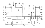
- 半導体デバイスにおける相互接続層上の一対の相互接続部の間にエアーギャップを形成する方法であって、
半導体デバイスの複数の絶縁層を堆積するステップと、
第一ハードマスク絶縁層を前記複数の絶縁層上に堆積するステップと、
前記第一ハードマスク絶縁層の一部を除去して、相互接続部が形成されるべき離間した前記複数の絶縁層の最上部領域を露出させるステップと、
第二ハードマスク絶縁層を、前記第一ハードマスク絶縁層及び前記複数の絶縁層の最上部の露出領域の上に堆積するステップと、
前記第一ハードマスク絶縁層上の前記第二ハードマスク絶縁層の全部及び複数の絶縁層の最上部の露出領域の上の前記第二ハードマスク絶縁層の一部を除去して、相互接続部が形成されるべき複数の絶縁層の最上部領域を露出させ、前記相互接続部が形成されるべき前記複数の絶縁層の最上部領域に隣接して第二ハードマスク・スペーサは残すようにするステップと、
前記第一ハードマスク絶縁層及び前記第二ハードマスク・スペーサを用いて、下方の複数の絶縁層の少なくとも一つをエッチングして、相互接続部の開口部を形成するステップと、
コンフォーマル絶縁層を堆積し、このコンフォーマル絶縁層を指向性エッチングして、前記相互接続部の開口部の側壁にスペーサを形成するステップと、
前記コンフォーマル絶縁層スペーサに隣接して導電性金属を堆積して、前記相互接続部の開口部に相互接続部を形成するステップと、
2つの前記コンフォーマル絶縁層スペーサの間の前記第一ハードマスク絶縁層及び前記下方の複数の絶縁層の一部をエッチングし、前記コンフォーマル絶縁層スペーサに隣接して第二ハードマスク・スペーサを残すようにして、前記相互接続部の少なくとも一方の下方に延びるエアーギャップを形成するステップと、
少なくとも一つの絶縁層を、前記エアーギャップ上と、前記相互接続部及び前記コンフォーマル絶縁層スペーサ上と、第二ハードマスク・スペーサ上に堆積して、前記エアーギャップを密閉するステップと、
を含む方法。 - 前記エアーギャップが前記相互接続部の上方に、前記少なくとも一つの絶縁層の中まで延びる、請求項1に記載の方法。
- 半導体デバイスの複数の絶縁層を堆積する前記ステップが、半導体デバイスの第一絶縁キャップ層を堆積するステップと、第二絶縁層を前記第一絶縁キャップ層上に堆積するステップと、第三絶縁層のエッチング停止層を前記第二絶縁層上に堆積するステップと、第四絶縁層を前記第三絶縁エッチング停止層上に堆積するステップとを含み、
前記第一ハードマスク絶縁層の一部を除去する前記ステップが、相互接続部が形成されるべき前記第四絶縁層の領域を露出させ、
前記コンフォーマル絶縁層スペーサ間には、前記第一ハードマスク絶縁層と、前記第四絶縁層と、前記第三絶縁エッチング停止層とのエッチングされた部分があり、前記コンフォーマル絶縁層スペーサに隣接して前記第二ハードマスク・スペーサを残すようにして、前記相互接続部の少なくとも一方の下方に延びる前記エアーギャップを形成する、請求項1に記載の方法。 - 前記相互接続部上の前記少なくとも一つの絶縁層が、前記相互接続部のための第五絶縁キャップ層と、前記キャップ層の上方の第六絶縁層とを含み、前記エアーギャップが前記第五絶縁キャップ層を完全に貫通して、前記第六絶縁層の一部の中まで延びる、請求項3に記載の方法。
Applications Claiming Priority (3)
| Application Number | Priority Date | Filing Date | Title |
|---|---|---|---|
| US10/605,440 US7071532B2 (en) | 2003-09-30 | 2003-09-30 | Adjustable self-aligned air gap dielectric for low capacitance wiring |
| US10/605,440 | 2003-09-30 | ||
| PCT/US2004/032404 WO2005034200A2 (en) | 2003-09-30 | 2004-09-30 | Adjustable self-aligned air gap dielectric for low capacitance wiring |
Publications (2)
| Publication Number | Publication Date |
|---|---|
| JP2007507903A JP2007507903A (ja) | 2007-03-29 |
| JP5004585B2 true JP5004585B2 (ja) | 2012-08-22 |
Family
ID=34375676
Family Applications (1)
| Application Number | Title | Priority Date | Filing Date |
|---|---|---|---|
| JP2006534155A Expired - Fee Related JP5004585B2 (ja) | 2003-09-30 | 2004-09-30 | 半導体デバイスにおける相互接続層上の一対の相互接続部の間にエアーギャップを形成する方法 |
Country Status (8)
| Country | Link |
|---|---|
| US (2) | US7071532B2 (ja) |
| EP (1) | EP1668692B1 (ja) |
| JP (1) | JP5004585B2 (ja) |
| KR (1) | KR100800360B1 (ja) |
| CN (1) | CN100466219C (ja) |
| AT (1) | ATE547809T1 (ja) |
| TW (1) | TWI319903B (ja) |
| WO (1) | WO2005034200A2 (ja) |
Families Citing this family (194)
| Publication number | Priority date | Publication date | Assignee | Title |
|---|---|---|---|---|
| KR100579846B1 (ko) * | 2003-12-11 | 2006-05-12 | 동부일렉트로닉스 주식회사 | 반도체 소자의 금속 배선층 및 이의 제조 방법 |
| DE102004003337A1 (de) * | 2004-01-22 | 2005-08-18 | Infineon Technologies Ag | Plasmaangeregtes chemisches Gasphasenabscheide-Verfahren, Silizium-Sauerstoff-Stickstoff-haltiges Material und Schicht-Anordnung |
| KR20050114784A (ko) * | 2004-06-01 | 2005-12-07 | 동부아남반도체 주식회사 | 반도체 소자의 구리배선 형성방법 |
| DE102004050391B4 (de) * | 2004-10-15 | 2007-02-08 | Infineon Technologies Ag | Verfahren zum Herstellen einer Schicht-Anordnung und Schicht-Anordnung |
| KR100632653B1 (ko) * | 2005-04-22 | 2006-10-12 | 주식회사 하이닉스반도체 | 반도체 소자의 비트라인 형성방법 |
| US7629225B2 (en) * | 2005-06-13 | 2009-12-08 | Infineon Technologies Ag | Methods of manufacturing semiconductor devices and structures thereof |
| EP1837905A3 (en) * | 2005-07-12 | 2008-12-31 | STMicroelectronics (Crolles 2) SAS | Interconnect structure having cavities in its dielectric portion |
| KR100672731B1 (ko) * | 2005-10-04 | 2007-01-24 | 동부일렉트로닉스 주식회사 | 반도체 소자의 금속배선 형성방법 |
| CN1996589B (zh) * | 2005-12-31 | 2010-10-13 | 上海集成电路研发中心有限公司 | 利用空气填充降低介电常数的大马士革结构及其制造方法 |
| WO2007113108A1 (en) | 2006-03-30 | 2007-10-11 | Koninklijke Philips Electronics N.V. | Improving control of localized air gap formation in an interconnect stack |
| US7951723B2 (en) * | 2006-10-24 | 2011-05-31 | Taiwan Semiconductor Manufacturing Company, Ltd. | Integrated etch and supercritical CO2 process and chamber design |
| WO2008056295A1 (en) * | 2006-11-09 | 2008-05-15 | Nxp B.V. | A semiconductor device and a method of manufacturing thereof |
| US7973409B2 (en) * | 2007-01-22 | 2011-07-05 | International Business Machines Corporation | Hybrid interconnect structure for performance improvement and reliability enhancement |
| US20080185722A1 (en) * | 2007-02-05 | 2008-08-07 | Chung-Shi Liu | Formation process of interconnect structures with air-gaps and sidewall spacers |
| DE102007020269A1 (de) * | 2007-04-30 | 2008-11-06 | Advanced Micro Devices, Inc., Sunnyvale | Halbleiterstruktur mit einer elektrischen Verbindung und Verfahren zu ihrer Herstellung |
| KR100854860B1 (ko) * | 2007-06-27 | 2008-08-28 | 주식회사 하이닉스반도체 | 메모리 소자의 제조방법 |
| US20090072409A1 (en) * | 2007-09-14 | 2009-03-19 | International Business Machines Corporation | Interconnect Structures Incorporating Air-Gap Spacers |
| US20090075470A1 (en) * | 2007-09-14 | 2009-03-19 | International Business Machines Corporation | Method for Manufacturing Interconnect Structures Incorporating Air-Gap Spacers |
| US8476758B2 (en) * | 2008-01-09 | 2013-07-02 | International Business Machines Corporation | Airgap-containing interconnect structure with patternable low-k material and method of fabricating |
| US8108820B2 (en) * | 2008-09-11 | 2012-01-31 | International Business Machines Corporation | Enhanced conductivity in an airgapped integrated circuit |
| JP5491077B2 (ja) * | 2009-06-08 | 2014-05-14 | キヤノン株式会社 | 半導体装置、及び半導体装置の製造方法 |
| US8519540B2 (en) | 2009-06-16 | 2013-08-27 | International Business Machines Corporation | Self-aligned dual damascene BEOL structures with patternable low- K material and methods of forming same |
| US8659115B2 (en) * | 2009-06-17 | 2014-02-25 | International Business Machines Corporation | Airgap-containing interconnect structure with improved patternable low-K material and method of fabricating |
| US8163658B2 (en) | 2009-08-24 | 2012-04-24 | International Business Machines Corporation | Multiple patterning using improved patternable low-k dielectric materials |
| US8003516B2 (en) * | 2009-08-26 | 2011-08-23 | International Business Machines Corporation | BEOL interconnect structures and related fabrication methods |
| US7790601B1 (en) * | 2009-09-17 | 2010-09-07 | International Business Machines Corporation | Forming interconnects with air gaps |
| US8202783B2 (en) | 2009-09-29 | 2012-06-19 | International Business Machines Corporation | Patternable low-k dielectric interconnect structure with a graded cap layer and method of fabrication |
| US8637395B2 (en) | 2009-11-16 | 2014-01-28 | International Business Machines Corporation | Methods for photo-patternable low-k (PPLK) integration with curing after pattern transfer |
| US8367540B2 (en) * | 2009-11-19 | 2013-02-05 | International Business Machines Corporation | Interconnect structure including a modified photoresist as a permanent interconnect dielectric and method of fabricating same |
| US8642252B2 (en) | 2010-03-10 | 2014-02-04 | International Business Machines Corporation | Methods for fabrication of an air gap-containing interconnect structure |
| US8896120B2 (en) | 2010-04-27 | 2014-11-25 | International Business Machines Corporation | Structures and methods for air gap integration |
| US8357609B2 (en) * | 2010-05-04 | 2013-01-22 | Globalfoundries Inc. | Dual damascene-like subtractive metal etch scheme |
| US8241992B2 (en) | 2010-05-10 | 2012-08-14 | International Business Machines Corporation | Method for air gap interconnect integration using photo-patternable low k material |
| US8373271B2 (en) | 2010-05-27 | 2013-02-12 | International Business Machines Corporation | Interconnect structure with an oxygen-doped SiC antireflective coating and method of fabrication |
| US9324576B2 (en) | 2010-05-27 | 2016-04-26 | Applied Materials, Inc. | Selective etch for silicon films |
| US8497203B2 (en) | 2010-08-13 | 2013-07-30 | International Business Machines Corporation | Semiconductor structures and methods of manufacture |
| US10283321B2 (en) | 2011-01-18 | 2019-05-07 | Applied Materials, Inc. | Semiconductor processing system and methods using capacitively coupled plasma |
| US8999856B2 (en) | 2011-03-14 | 2015-04-07 | Applied Materials, Inc. | Methods for etch of sin films |
| US9064815B2 (en) | 2011-03-14 | 2015-06-23 | Applied Materials, Inc. | Methods for etch of metal and metal-oxide films |
| US9054160B2 (en) | 2011-04-15 | 2015-06-09 | International Business Machines Corporation | Interconnect structure and method for fabricating on-chip interconnect structures by image reversal |
| US8900988B2 (en) | 2011-04-15 | 2014-12-02 | International Business Machines Corporation | Method for forming self-aligned airgap interconnect structures |
| US8890318B2 (en) | 2011-04-15 | 2014-11-18 | International Business Machines Corporation | Middle of line structures |
| US8822137B2 (en) | 2011-08-03 | 2014-09-02 | International Business Machines Corporation | Self-aligned fine pitch permanent on-chip interconnect structures and method of fabrication |
| US20130062732A1 (en) | 2011-09-08 | 2013-03-14 | International Business Machines Corporation | Interconnect structures with functional components and methods for fabrication |
| US8808563B2 (en) | 2011-10-07 | 2014-08-19 | Applied Materials, Inc. | Selective etch of silicon by way of metastable hydrogen termination |
| CN103137545B (zh) * | 2011-11-25 | 2015-08-05 | 中芯国际集成电路制造(上海)有限公司 | 半导体器件及其形成方法 |
| CN103165519B (zh) * | 2011-12-08 | 2016-07-27 | 中芯国际集成电路制造(上海)有限公司 | 一种半导体器件的制造方法 |
| CN103178000B (zh) * | 2011-12-20 | 2014-11-05 | 中芯国际集成电路制造(上海)有限公司 | 半导体器件及其形成方法 |
| US9087753B2 (en) | 2012-05-10 | 2015-07-21 | International Business Machines Corporation | Printed transistor and fabrication method |
| US9267739B2 (en) | 2012-07-18 | 2016-02-23 | Applied Materials, Inc. | Pedestal with multi-zone temperature control and multiple purge capabilities |
| US9373517B2 (en) | 2012-08-02 | 2016-06-21 | Applied Materials, Inc. | Semiconductor processing with DC assisted RF power for improved control |
| KR101921465B1 (ko) | 2012-08-22 | 2018-11-26 | 삼성전자 주식회사 | 반도체 소자 및 이의 제조 방법 |
| US9034770B2 (en) | 2012-09-17 | 2015-05-19 | Applied Materials, Inc. | Differential silicon oxide etch |
| US9023734B2 (en) | 2012-09-18 | 2015-05-05 | Applied Materials, Inc. | Radical-component oxide etch |
| US9390937B2 (en) | 2012-09-20 | 2016-07-12 | Applied Materials, Inc. | Silicon-carbon-nitride selective etch |
| US9132436B2 (en) | 2012-09-21 | 2015-09-15 | Applied Materials, Inc. | Chemical control features in wafer process equipment |
| US8847401B2 (en) | 2012-10-31 | 2014-09-30 | International Business Machines Corporation | Semiconductor structure incorporating a contact sidewall spacer with a self-aligned airgap and a method of forming the semiconductor structure |
| US8969212B2 (en) | 2012-11-20 | 2015-03-03 | Applied Materials, Inc. | Dry-etch selectivity |
| US8980763B2 (en) | 2012-11-30 | 2015-03-17 | Applied Materials, Inc. | Dry-etch for selective tungsten removal |
| US9111877B2 (en) | 2012-12-18 | 2015-08-18 | Applied Materials, Inc. | Non-local plasma oxide etch |
| US8921234B2 (en) | 2012-12-21 | 2014-12-30 | Applied Materials, Inc. | Selective titanium nitride etching |
| US10256079B2 (en) | 2013-02-08 | 2019-04-09 | Applied Materials, Inc. | Semiconductor processing systems having multiple plasma configurations |
| US9362130B2 (en) | 2013-03-01 | 2016-06-07 | Applied Materials, Inc. | Enhanced etching processes using remote plasma sources |
| US9040422B2 (en) | 2013-03-05 | 2015-05-26 | Applied Materials, Inc. | Selective titanium nitride removal |
| US20140271097A1 (en) | 2013-03-15 | 2014-09-18 | Applied Materials, Inc. | Processing systems and methods for halide scavenging |
| US9493879B2 (en) | 2013-07-12 | 2016-11-15 | Applied Materials, Inc. | Selective sputtering for pattern transfer |
| US9773648B2 (en) | 2013-08-30 | 2017-09-26 | Applied Materials, Inc. | Dual discharge modes operation for remote plasma |
| US9576809B2 (en) | 2013-11-04 | 2017-02-21 | Applied Materials, Inc. | Etch suppression with germanium |
| US9520303B2 (en) | 2013-11-12 | 2016-12-13 | Applied Materials, Inc. | Aluminum selective etch |
| US9159671B2 (en) | 2013-11-19 | 2015-10-13 | International Business Machines Corporation | Copper wire and dielectric with air gaps |
| US9245762B2 (en) | 2013-12-02 | 2016-01-26 | Applied Materials, Inc. | Procedure for etch rate consistency |
| US9287095B2 (en) | 2013-12-17 | 2016-03-15 | Applied Materials, Inc. | Semiconductor system assemblies and methods of operation |
| US9287134B2 (en) | 2014-01-17 | 2016-03-15 | Applied Materials, Inc. | Titanium oxide etch |
| US9293568B2 (en) | 2014-01-27 | 2016-03-22 | Applied Materials, Inc. | Method of fin patterning |
| US9396989B2 (en) | 2014-01-27 | 2016-07-19 | Applied Materials, Inc. | Air gaps between copper lines |
| US9385028B2 (en) | 2014-02-03 | 2016-07-05 | Applied Materials, Inc. | Air gap process |
| US9499898B2 (en) | 2014-03-03 | 2016-11-22 | Applied Materials, Inc. | Layered thin film heater and method of fabrication |
| US9299575B2 (en) | 2014-03-17 | 2016-03-29 | Applied Materials, Inc. | Gas-phase tungsten etch |
| US9299537B2 (en) | 2014-03-20 | 2016-03-29 | Applied Materials, Inc. | Radial waveguide systems and methods for post-match control of microwaves |
| US9299538B2 (en) | 2014-03-20 | 2016-03-29 | Applied Materials, Inc. | Radial waveguide systems and methods for post-match control of microwaves |
| US9903020B2 (en) | 2014-03-31 | 2018-02-27 | Applied Materials, Inc. | Generation of compact alumina passivation layers on aluminum plasma equipment components |
| US9269590B2 (en) | 2014-04-07 | 2016-02-23 | Applied Materials, Inc. | Spacer formation |
| US9309598B2 (en) | 2014-05-28 | 2016-04-12 | Applied Materials, Inc. | Oxide and metal removal |
| US9406523B2 (en) | 2014-06-19 | 2016-08-02 | Applied Materials, Inc. | Highly selective doped oxide removal method |
| US9378969B2 (en) | 2014-06-19 | 2016-06-28 | Applied Materials, Inc. | Low temperature gas-phase carbon removal |
| US9425096B2 (en) | 2014-07-14 | 2016-08-23 | Qualcomm Incorporated | Air gap between tungsten metal lines for interconnects with reduced RC delay |
| US9425058B2 (en) | 2014-07-24 | 2016-08-23 | Applied Materials, Inc. | Simplified litho-etch-litho-etch process |
| US9378978B2 (en) | 2014-07-31 | 2016-06-28 | Applied Materials, Inc. | Integrated oxide recess and floating gate fin trimming |
| US9159606B1 (en) * | 2014-07-31 | 2015-10-13 | Applied Materials, Inc. | Metal air gap |
| US9496167B2 (en) | 2014-07-31 | 2016-11-15 | Applied Materials, Inc. | Integrated bit-line airgap formation and gate stack post clean |
| US9659753B2 (en) | 2014-08-07 | 2017-05-23 | Applied Materials, Inc. | Grooved insulator to reduce leakage current |
| US9553102B2 (en) | 2014-08-19 | 2017-01-24 | Applied Materials, Inc. | Tungsten separation |
| US9355856B2 (en) | 2014-09-12 | 2016-05-31 | Applied Materials, Inc. | V trench dry etch |
| US9478434B2 (en) | 2014-09-24 | 2016-10-25 | Applied Materials, Inc. | Chlorine-based hardmask removal |
| US9368364B2 (en) | 2014-09-24 | 2016-06-14 | Applied Materials, Inc. | Silicon etch process with tunable selectivity to SiO2 and other materials |
| US9613822B2 (en) | 2014-09-25 | 2017-04-04 | Applied Materials, Inc. | Oxide etch selectivity enhancement |
| US9355922B2 (en) | 2014-10-14 | 2016-05-31 | Applied Materials, Inc. | Systems and methods for internal surface conditioning in plasma processing equipment |
| US9966240B2 (en) | 2014-10-14 | 2018-05-08 | Applied Materials, Inc. | Systems and methods for internal surface conditioning assessment in plasma processing equipment |
| US9431294B2 (en) * | 2014-10-28 | 2016-08-30 | GlobalFoundries, Inc. | Methods of producing integrated circuits with an air gap |
| US11637002B2 (en) | 2014-11-26 | 2023-04-25 | Applied Materials, Inc. | Methods and systems to enhance process uniformity |
| US9299583B1 (en) | 2014-12-05 | 2016-03-29 | Applied Materials, Inc. | Aluminum oxide selective etch |
| US10573496B2 (en) | 2014-12-09 | 2020-02-25 | Applied Materials, Inc. | Direct outlet toroidal plasma source |
| US10224210B2 (en) | 2014-12-09 | 2019-03-05 | Applied Materials, Inc. | Plasma processing system with direct outlet toroidal plasma source |
| US9502258B2 (en) | 2014-12-23 | 2016-11-22 | Applied Materials, Inc. | Anisotropic gap etch |
| US9343272B1 (en) | 2015-01-08 | 2016-05-17 | Applied Materials, Inc. | Self-aligned process |
| US11257693B2 (en) | 2015-01-09 | 2022-02-22 | Applied Materials, Inc. | Methods and systems to improve pedestal temperature control |
| US9373522B1 (en) | 2015-01-22 | 2016-06-21 | Applied Mateials, Inc. | Titanium nitride removal |
| US9449846B2 (en) | 2015-01-28 | 2016-09-20 | Applied Materials, Inc. | Vertical gate separation |
| US9728437B2 (en) | 2015-02-03 | 2017-08-08 | Applied Materials, Inc. | High temperature chuck for plasma processing systems |
| US20160225652A1 (en) | 2015-02-03 | 2016-08-04 | Applied Materials, Inc. | Low temperature chuck for plasma processing systems |
| US9881805B2 (en) | 2015-03-02 | 2018-01-30 | Applied Materials, Inc. | Silicon selective removal |
| US9691645B2 (en) | 2015-08-06 | 2017-06-27 | Applied Materials, Inc. | Bolted wafer chuck thermal management systems and methods for wafer processing systems |
| US9741593B2 (en) | 2015-08-06 | 2017-08-22 | Applied Materials, Inc. | Thermal management systems and methods for wafer processing systems |
| US9349605B1 (en) | 2015-08-07 | 2016-05-24 | Applied Materials, Inc. | Oxide etch selectivity systems and methods |
| US10504700B2 (en) | 2015-08-27 | 2019-12-10 | Applied Materials, Inc. | Plasma etching systems and methods with secondary plasma injection |
| US10256141B2 (en) * | 2015-09-23 | 2019-04-09 | Intel Corporation | Maskless air gap to prevent via punch through |
| KR102334736B1 (ko) * | 2015-12-03 | 2021-12-03 | 삼성전자주식회사 | 반도체 장치 및 그 제조 방법 |
| US9905463B2 (en) | 2015-12-15 | 2018-02-27 | International Business Machines Corporation | Self-aligned low dielectric constant gate cap and a method of forming the same |
| KR102616823B1 (ko) * | 2015-12-16 | 2023-12-22 | 삼성전자주식회사 | 반도체 장치 |
| US9349687B1 (en) | 2015-12-19 | 2016-05-24 | International Business Machines Corporation | Advanced manganese/manganese nitride cap/etch mask for air gap formation scheme in nanocopper low-K interconnect |
| US10504754B2 (en) | 2016-05-19 | 2019-12-10 | Applied Materials, Inc. | Systems and methods for improved semiconductor etching and component protection |
| US10522371B2 (en) | 2016-05-19 | 2019-12-31 | Applied Materials, Inc. | Systems and methods for improved semiconductor etching and component protection |
| US9865484B1 (en) | 2016-06-29 | 2018-01-09 | Applied Materials, Inc. | Selective etch using material modification and RF pulsing |
| US9859212B1 (en) | 2016-07-12 | 2018-01-02 | International Business Machines Corporation | Multi-level air gap formation in dual-damascene structure |
| US10032711B2 (en) | 2016-07-25 | 2018-07-24 | International Business Machines Corporation | Integrating metal-insulator-metal capacitors with air gap process flow |
| US10062575B2 (en) | 2016-09-09 | 2018-08-28 | Applied Materials, Inc. | Poly directional etch by oxidation |
| US10629473B2 (en) | 2016-09-09 | 2020-04-21 | Applied Materials, Inc. | Footing removal for nitride spacer |
| US9786553B1 (en) | 2016-09-16 | 2017-10-10 | International Business Machines Corporation | Advanced BEOL interconnect structure containing uniform air gaps |
| US9721789B1 (en) | 2016-10-04 | 2017-08-01 | Applied Materials, Inc. | Saving ion-damaged spacers |
| US10062585B2 (en) | 2016-10-04 | 2018-08-28 | Applied Materials, Inc. | Oxygen compatible plasma source |
| US10546729B2 (en) | 2016-10-04 | 2020-01-28 | Applied Materials, Inc. | Dual-channel showerhead with improved profile |
| US9934942B1 (en) | 2016-10-04 | 2018-04-03 | Applied Materials, Inc. | Chamber with flow-through source |
| US10062579B2 (en) | 2016-10-07 | 2018-08-28 | Applied Materials, Inc. | Selective SiN lateral recess |
| US9947549B1 (en) | 2016-10-10 | 2018-04-17 | Applied Materials, Inc. | Cobalt-containing material removal |
| US9768034B1 (en) | 2016-11-11 | 2017-09-19 | Applied Materials, Inc. | Removal methods for high aspect ratio structures |
| US10163696B2 (en) | 2016-11-11 | 2018-12-25 | Applied Materials, Inc. | Selective cobalt removal for bottom up gapfill |
| US10026621B2 (en) | 2016-11-14 | 2018-07-17 | Applied Materials, Inc. | SiN spacer profile patterning |
| US10242908B2 (en) | 2016-11-14 | 2019-03-26 | Applied Materials, Inc. | Airgap formation with damage-free copper |
| US10566206B2 (en) | 2016-12-27 | 2020-02-18 | Applied Materials, Inc. | Systems and methods for anisotropic material breakthrough |
| US10403507B2 (en) | 2017-02-03 | 2019-09-03 | Applied Materials, Inc. | Shaped etch profile with oxidation |
| US10431429B2 (en) | 2017-02-03 | 2019-10-01 | Applied Materials, Inc. | Systems and methods for radial and azimuthal control of plasma uniformity |
| US10043684B1 (en) | 2017-02-06 | 2018-08-07 | Applied Materials, Inc. | Self-limiting atomic thermal etching systems and methods |
| US10319739B2 (en) | 2017-02-08 | 2019-06-11 | Applied Materials, Inc. | Accommodating imperfectly aligned memory holes |
| US10943834B2 (en) | 2017-03-13 | 2021-03-09 | Applied Materials, Inc. | Replacement contact process |
| US9911652B1 (en) | 2017-03-29 | 2018-03-06 | International Business Machines Corporation | Forming self-aligned vias and air-gaps in semiconductor fabrication |
| US10319649B2 (en) | 2017-04-11 | 2019-06-11 | Applied Materials, Inc. | Optical emission spectroscopy (OES) for remote plasma monitoring |
| JP7176860B6 (ja) | 2017-05-17 | 2022-12-16 | アプライド マテリアルズ インコーポレイテッド | 前駆体の流れを改善する半導体処理チャンバ |
| US11276559B2 (en) | 2017-05-17 | 2022-03-15 | Applied Materials, Inc. | Semiconductor processing chamber for multiple precursor flow |
| US11276590B2 (en) | 2017-05-17 | 2022-03-15 | Applied Materials, Inc. | Multi-zone semiconductor substrate supports |
| US10497579B2 (en) | 2017-05-31 | 2019-12-03 | Applied Materials, Inc. | Water-free etching methods |
| US10049891B1 (en) | 2017-05-31 | 2018-08-14 | Applied Materials, Inc. | Selective in situ cobalt residue removal |
| US10920320B2 (en) | 2017-06-16 | 2021-02-16 | Applied Materials, Inc. | Plasma health determination in semiconductor substrate processing reactors |
| US10541246B2 (en) | 2017-06-26 | 2020-01-21 | Applied Materials, Inc. | 3D flash memory cells which discourage cross-cell electrical tunneling |
| US10727080B2 (en) | 2017-07-07 | 2020-07-28 | Applied Materials, Inc. | Tantalum-containing material removal |
| US10541184B2 (en) | 2017-07-11 | 2020-01-21 | Applied Materials, Inc. | Optical emission spectroscopic techniques for monitoring etching |
| US10354889B2 (en) | 2017-07-17 | 2019-07-16 | Applied Materials, Inc. | Non-halogen etching of silicon-containing materials |
| US10043674B1 (en) | 2017-08-04 | 2018-08-07 | Applied Materials, Inc. | Germanium etching systems and methods |
| US10170336B1 (en) | 2017-08-04 | 2019-01-01 | Applied Materials, Inc. | Methods for anisotropic control of selective silicon removal |
| US10297458B2 (en) | 2017-08-07 | 2019-05-21 | Applied Materials, Inc. | Process window widening using coated parts in plasma etch processes |
| US10629478B2 (en) * | 2017-08-22 | 2020-04-21 | International Business Machines Corporation | Dual-damascene formation with dielectric spacer and thin liner |
| US10283324B1 (en) | 2017-10-24 | 2019-05-07 | Applied Materials, Inc. | Oxygen treatment for nitride etching |
| US10128086B1 (en) | 2017-10-24 | 2018-11-13 | Applied Materials, Inc. | Silicon pretreatment for nitride removal |
| US10256112B1 (en) | 2017-12-08 | 2019-04-09 | Applied Materials, Inc. | Selective tungsten removal |
| US10903054B2 (en) | 2017-12-19 | 2021-01-26 | Applied Materials, Inc. | Multi-zone gas distribution systems and methods |
| US11328909B2 (en) | 2017-12-22 | 2022-05-10 | Applied Materials, Inc. | Chamber conditioning and removal processes |
| US10854426B2 (en) | 2018-01-08 | 2020-12-01 | Applied Materials, Inc. | Metal recess for semiconductor structures |
| US10679870B2 (en) | 2018-02-15 | 2020-06-09 | Applied Materials, Inc. | Semiconductor processing chamber multistage mixing apparatus |
| US10964512B2 (en) | 2018-02-15 | 2021-03-30 | Applied Materials, Inc. | Semiconductor processing chamber multistage mixing apparatus and methods |
| TWI766433B (zh) | 2018-02-28 | 2022-06-01 | 美商應用材料股份有限公司 | 形成氣隙的系統及方法 |
| US10593560B2 (en) | 2018-03-01 | 2020-03-17 | Applied Materials, Inc. | Magnetic induction plasma source for semiconductor processes and equipment |
| US10319600B1 (en) | 2018-03-12 | 2019-06-11 | Applied Materials, Inc. | Thermal silicon etch |
| US10497573B2 (en) | 2018-03-13 | 2019-12-03 | Applied Materials, Inc. | Selective atomic layer etching of semiconductor materials |
| US10573527B2 (en) | 2018-04-06 | 2020-02-25 | Applied Materials, Inc. | Gas-phase selective etching systems and methods |
| US10490406B2 (en) | 2018-04-10 | 2019-11-26 | Appled Materials, Inc. | Systems and methods for material breakthrough |
| US10699879B2 (en) | 2018-04-17 | 2020-06-30 | Applied Materials, Inc. | Two piece electrode assembly with gap for plasma control |
| US10886137B2 (en) | 2018-04-30 | 2021-01-05 | Applied Materials, Inc. | Selective nitride removal |
| US10319629B1 (en) * | 2018-05-08 | 2019-06-11 | International Business Machines Corporation | Skip via for metal interconnects |
| US11469189B2 (en) * | 2018-06-29 | 2022-10-11 | Intel Corporation | Inductor and transmission line with air gap |
| US10755941B2 (en) | 2018-07-06 | 2020-08-25 | Applied Materials, Inc. | Self-limiting selective etching systems and methods |
| US10872778B2 (en) | 2018-07-06 | 2020-12-22 | Applied Materials, Inc. | Systems and methods utilizing solid-phase etchants |
| US10672642B2 (en) | 2018-07-24 | 2020-06-02 | Applied Materials, Inc. | Systems and methods for pedestal configuration |
| US10892198B2 (en) | 2018-09-14 | 2021-01-12 | Applied Materials, Inc. | Systems and methods for improved performance in semiconductor processing |
| US11049755B2 (en) | 2018-09-14 | 2021-06-29 | Applied Materials, Inc. | Semiconductor substrate supports with embedded RF shield |
| US11062887B2 (en) | 2018-09-17 | 2021-07-13 | Applied Materials, Inc. | High temperature RF heater pedestals |
| US11417534B2 (en) | 2018-09-21 | 2022-08-16 | Applied Materials, Inc. | Selective material removal |
| US11682560B2 (en) | 2018-10-11 | 2023-06-20 | Applied Materials, Inc. | Systems and methods for hafnium-containing film removal |
| US11121002B2 (en) | 2018-10-24 | 2021-09-14 | Applied Materials, Inc. | Systems and methods for etching metals and metal derivatives |
| US11437242B2 (en) | 2018-11-27 | 2022-09-06 | Applied Materials, Inc. | Selective removal of silicon-containing materials |
| US11721527B2 (en) | 2019-01-07 | 2023-08-08 | Applied Materials, Inc. | Processing chamber mixing systems |
| US10920319B2 (en) | 2019-01-11 | 2021-02-16 | Applied Materials, Inc. | Ceramic showerheads with conductive electrodes |
| CN112885773B (zh) * | 2019-11-29 | 2024-10-22 | 长鑫存储技术有限公司 | 半导体结构及其制作方法 |
| US11289371B2 (en) | 2020-01-23 | 2022-03-29 | International Business Machines Corporation | Top vias with selectively retained etch stops |
| US20210265205A1 (en) * | 2020-02-25 | 2021-08-26 | Tokyo Electron Limited | Dielectric etch stop layer for reactive ion etch (rie) lag reduction and chamfer corner protection |
| CN111501025B (zh) * | 2020-04-23 | 2022-05-27 | 北京北方华创微电子装备有限公司 | 沉积设备 |
Family Cites Families (24)
| Publication number | Priority date | Publication date | Assignee | Title |
|---|---|---|---|---|
| US5117276A (en) * | 1989-08-14 | 1992-05-26 | Fairchild Camera And Instrument Corp. | High performance interconnect system for an integrated circuit |
| JPH0722583A (ja) * | 1992-12-15 | 1995-01-24 | Internatl Business Mach Corp <Ibm> | 多層回路装置 |
| US5324683A (en) | 1993-06-02 | 1994-06-28 | Motorola, Inc. | Method of forming a semiconductor structure having an air region |
| US6281585B1 (en) | 1997-06-30 | 2001-08-28 | Philips Electronics North America Corporation | Air gap dielectric in self-aligned via structures |
| US6184121B1 (en) * | 1997-07-10 | 2001-02-06 | International Business Machines Corporation | Chip interconnect wiring structure with low dielectric constant insulator and methods for fabricating the same |
| JP2971454B2 (ja) * | 1997-08-21 | 1999-11-08 | 松下電子工業株式会社 | 半導体装置とその製造方法 |
| US6333255B1 (en) * | 1997-08-21 | 2001-12-25 | Matsushita Electronics Corporation | Method for making semiconductor device containing low carbon film for interconnect structures |
| US6242336B1 (en) * | 1997-11-06 | 2001-06-05 | Matsushita Electronics Corporation | Semiconductor device having multilevel interconnection structure and method for fabricating the same |
| FR2784230B1 (fr) * | 1998-10-05 | 2000-12-29 | St Microelectronics Sa | Procede de realisation d'un isolement inter et/ou intra-metallique par air dans un circuit integre et circuit integre obtenu |
| US6211561B1 (en) * | 1998-11-16 | 2001-04-03 | Conexant Systems, Inc. | Interconnect structure and method employing air gaps between metal lines and between metal layers |
| US6150232A (en) | 1999-02-05 | 2000-11-21 | Chartered Semiconductor Manufacturing Ltd. | Formation of low k dielectric |
| US6177329B1 (en) | 1999-04-15 | 2001-01-23 | Kurt Pang | Integrated circuit structures having gas pockets and method for forming integrated circuit structures having gas pockets |
| US6211057B1 (en) * | 1999-09-03 | 2001-04-03 | Taiwan Semiconductor Manufacturing Company | Method for manufacturing arch air gap in multilevel interconnection |
| US6200900B1 (en) | 1999-10-08 | 2001-03-13 | National Semiconductor Corporation | Method for formation of an air gap in an integrated circuit architecture |
| JP5156155B2 (ja) * | 1999-10-13 | 2013-03-06 | アプライド マテリアルズ インコーポレイテッド | 半導体集積回路を製造する方法 |
| KR20010063852A (ko) | 1999-12-24 | 2001-07-09 | 박종섭 | 반도체소자의 자기정렬적인 콘택 형성방법 |
| US6815329B2 (en) * | 2000-02-08 | 2004-11-09 | International Business Machines Corporation | Multilayer interconnect structure containing air gaps and method for making |
| US6329279B1 (en) | 2000-03-20 | 2001-12-11 | United Microelectronics Corp. | Method of fabricating metal interconnect structure having outer air spacer |
| US6423629B1 (en) | 2000-05-31 | 2002-07-23 | Kie Y. Ahn | Multilevel copper interconnects with low-k dielectrics and air gaps |
| US6413852B1 (en) | 2000-08-31 | 2002-07-02 | International Business Machines Corporation | Method of forming multilevel interconnect structure containing air gaps including utilizing both sacrificial and placeholder material |
| US6472266B1 (en) | 2001-06-18 | 2002-10-29 | Taiwan Semiconductor Manufacturing Company | Method to reduce bit line capacitance in cub drams |
| DE10140754A1 (de) * | 2001-08-20 | 2003-03-27 | Infineon Technologies Ag | Leiterbahnanordnung und Verfahren zum Herstellen einer Leiterbahnanordnung |
| US7138329B2 (en) * | 2002-11-15 | 2006-11-21 | United Microelectronics Corporation | Air gap for tungsten/aluminum plug applications |
| US6838354B2 (en) * | 2002-12-20 | 2005-01-04 | Freescale Semiconductor, Inc. | Method for forming a passivation layer for air gap formation |
-
2003
- 2003-09-30 US US10/605,440 patent/US7071532B2/en not_active Expired - Lifetime
-
2004
- 2004-09-20 TW TW093128432A patent/TWI319903B/zh not_active IP Right Cessation
- 2004-09-30 AT AT04809842T patent/ATE547809T1/de active
- 2004-09-30 EP EP04809842A patent/EP1668692B1/en not_active Expired - Lifetime
- 2004-09-30 WO PCT/US2004/032404 patent/WO2005034200A2/en not_active Ceased
- 2004-09-30 JP JP2006534155A patent/JP5004585B2/ja not_active Expired - Fee Related
- 2004-09-30 CN CNB2004800274275A patent/CN100466219C/zh not_active Expired - Fee Related
- 2004-09-30 KR KR1020067004177A patent/KR100800360B1/ko not_active Expired - Fee Related
-
2006
- 2006-05-05 US US11/418,921 patent/US7358148B2/en not_active Expired - Fee Related
Also Published As
| Publication number | Publication date |
|---|---|
| US7071532B2 (en) | 2006-07-04 |
| US7358148B2 (en) | 2008-04-15 |
| ATE547809T1 (de) | 2012-03-15 |
| CN1856872A (zh) | 2006-11-01 |
| TWI319903B (en) | 2010-01-21 |
| US20050067673A1 (en) | 2005-03-31 |
| EP1668692B1 (en) | 2012-02-29 |
| WO2005034200A3 (en) | 2005-09-29 |
| TW200520154A (en) | 2005-06-16 |
| US20060202302A1 (en) | 2006-09-14 |
| EP1668692A2 (en) | 2006-06-14 |
| CN100466219C (zh) | 2009-03-04 |
| WO2005034200A2 (en) | 2005-04-14 |
| EP1668692A4 (en) | 2007-05-09 |
| JP2007507903A (ja) | 2007-03-29 |
| KR100800360B1 (ko) | 2008-02-04 |
| KR20060072129A (ko) | 2006-06-27 |
Similar Documents
| Publication | Publication Date | Title |
|---|---|---|
| JP5004585B2 (ja) | 半導体デバイスにおける相互接続層上の一対の相互接続部の間にエアーギャップを形成する方法 | |
| US7037851B2 (en) | Methods for selective integration of airgaps and devices made by such methods | |
| US7319274B2 (en) | Methods for selective integration of airgaps and devices made by such methods | |
| US10546743B2 (en) | Advanced interconnect with air gap | |
| US8383507B2 (en) | Method for fabricating air gap interconnect structures | |
| US6984577B1 (en) | Damascene interconnect structure and fabrication method having air gaps between metal lines and metal layers | |
| US20040232552A1 (en) | Air gap dual damascene process and structure | |
| JP2009194286A (ja) | 半導体装置及びその製造方法 | |
| US20070120263A1 (en) | Conductor track arrangement and associated production method | |
| JP2006019480A (ja) | 半導体装置の製造方法 | |
| WO2007091574A1 (ja) | 多層配線構造および多層配線の製造方法 | |
| WO2010084535A1 (ja) | 半導体装置およびその製造方法 | |
| CN119650518B (zh) | 半导体结构的制备方法及半导体结构 | |
| CN100490115C (zh) | 具有含气隙的镶嵌结构的半导体器件的制造方法 | |
| JP3887175B2 (ja) | 半導体装置及びその製造方法 | |
| CN1447413A (zh) | 使用双波纹技术制造半导体器件的方法 | |
| CN113707602B (zh) | 半导体结构的形成方法及半导体结构 | |
| JP2024523801A (ja) | 後工程相互接続およびクロス・ポイントの絶縁を改善したサブトラクティブ金属エッチング | |
| CN113097127B (zh) | 半导体结构的形成方法 | |
| JP4383262B2 (ja) | 半導体装置及びその製造方法 | |
| US20010048162A1 (en) | Semiconductor device having a structure of a multilayer interconnection unit and manufacturing method thereof | |
| JP4967207B2 (ja) | 半導体装置の製造方法 | |
| EP1608013B1 (en) | Method of formation of airgaps around interconnecting line | |
| KR20110136498A (ko) | 반도체 소자의 제조 방법 | |
| KR20000021258A (ko) | 전자이탈을 억제하는 구조의 금속컨택 및 그형성방법 |
Legal Events
| Date | Code | Title | Description |
|---|---|---|---|
| A621 | Written request for application examination |
Free format text: JAPANESE INTERMEDIATE CODE: A621 Effective date: 20070816 |
|
| A977 | Report on retrieval |
Free format text: JAPANESE INTERMEDIATE CODE: A971007 Effective date: 20100805 |
|
| A131 | Notification of reasons for refusal |
Free format text: JAPANESE INTERMEDIATE CODE: A131 Effective date: 20110906 |
|
| A521 | Request for written amendment filed |
Free format text: JAPANESE INTERMEDIATE CODE: A523 Effective date: 20111121 |
|
| A131 | Notification of reasons for refusal |
Free format text: JAPANESE INTERMEDIATE CODE: A131 Effective date: 20120104 |
|
| A521 | Request for written amendment filed |
Free format text: JAPANESE INTERMEDIATE CODE: A523 Effective date: 20120329 |
|
| TRDD | Decision of grant or rejection written | ||
| A01 | Written decision to grant a patent or to grant a registration (utility model) |
Free format text: JAPANESE INTERMEDIATE CODE: A01 Effective date: 20120424 |
|
| A01 | Written decision to grant a patent or to grant a registration (utility model) |
Free format text: JAPANESE INTERMEDIATE CODE: A01 |
|
| A61 | First payment of annual fees (during grant procedure) |
Free format text: JAPANESE INTERMEDIATE CODE: A61 Effective date: 20120522 |
|
| FPAY | Renewal fee payment (event date is renewal date of database) |
Free format text: PAYMENT UNTIL: 20150601 Year of fee payment: 3 |
|
| R150 | Certificate of patent or registration of utility model |
Ref document number: 5004585 Country of ref document: JP Free format text: JAPANESE INTERMEDIATE CODE: R150 Free format text: JAPANESE INTERMEDIATE CODE: R150 |
|
| R250 | Receipt of annual fees |
Free format text: JAPANESE INTERMEDIATE CODE: R250 |
|
| R250 | Receipt of annual fees |
Free format text: JAPANESE INTERMEDIATE CODE: R250 |
|
| R250 | Receipt of annual fees |
Free format text: JAPANESE INTERMEDIATE CODE: R250 |
|
| LAPS | Cancellation because of no payment of annual fees |