JP5073694B2 - 半導体装置の製造方法 - Google Patents
半導体装置の製造方法 Download PDFInfo
- Publication number
- JP5073694B2 JP5073694B2 JP2009042807A JP2009042807A JP5073694B2 JP 5073694 B2 JP5073694 B2 JP 5073694B2 JP 2009042807 A JP2009042807 A JP 2009042807A JP 2009042807 A JP2009042807 A JP 2009042807A JP 5073694 B2 JP5073694 B2 JP 5073694B2
- Authority
- JP
- Japan
- Prior art keywords
- film
- insulating film
- oxide film
- trench
- manufacturing
- Prior art date
- Legal status (The legal status is an assumption and is not a legal conclusion. Google has not performed a legal analysis and makes no representation as to the accuracy of the status listed.)
- Expired - Lifetime
Links
- 239000004065 semiconductor Substances 0.000 title claims description 65
- 238000004519 manufacturing process Methods 0.000 title claims description 36
- VYPSYNLAJGMNEJ-UHFFFAOYSA-N Silicium dioxide Chemical compound O=[Si]=O VYPSYNLAJGMNEJ-UHFFFAOYSA-N 0.000 claims description 84
- 229910052814 silicon oxide Inorganic materials 0.000 claims description 84
- 238000000034 method Methods 0.000 claims description 65
- 239000000758 substrate Substances 0.000 claims description 51
- 229910021420 polycrystalline silicon Inorganic materials 0.000 claims description 26
- 238000005498 polishing Methods 0.000 claims description 25
- 229920005591 polysilicon Polymers 0.000 claims description 24
- 239000000126 substance Substances 0.000 claims description 6
- 238000000059 patterning Methods 0.000 claims description 5
- 230000001590 oxidative effect Effects 0.000 claims description 4
- 238000002955 isolation Methods 0.000 description 64
- 229910052581 Si3N4 Inorganic materials 0.000 description 36
- 238000005530 etching Methods 0.000 description 36
- HQVNEWCFYHHQES-UHFFFAOYSA-N silicon nitride Chemical compound N12[Si]34N5[Si]62N3[Si]51N64 HQVNEWCFYHHQES-UHFFFAOYSA-N 0.000 description 36
- XUIMIQQOPSSXEZ-UHFFFAOYSA-N Silicon Chemical compound [Si] XUIMIQQOPSSXEZ-UHFFFAOYSA-N 0.000 description 24
- 229910052710 silicon Inorganic materials 0.000 description 24
- 239000010703 silicon Substances 0.000 description 24
- 239000012535 impurity Substances 0.000 description 17
- 230000015572 biosynthetic process Effects 0.000 description 14
- 239000010410 layer Substances 0.000 description 12
- 238000001039 wet etching Methods 0.000 description 12
- 238000009792 diffusion process Methods 0.000 description 11
- 238000001312 dry etching Methods 0.000 description 11
- NBIIXXVUZAFLBC-UHFFFAOYSA-N Phosphoric acid Chemical compound OP(O)(O)=O NBIIXXVUZAFLBC-UHFFFAOYSA-N 0.000 description 10
- 230000007547 defect Effects 0.000 description 9
- 238000004518 low pressure chemical vapour deposition Methods 0.000 description 9
- 238000010438 heat treatment Methods 0.000 description 8
- 230000003647 oxidation Effects 0.000 description 8
- 238000007254 oxidation reaction Methods 0.000 description 8
- 238000000206 photolithography Methods 0.000 description 7
- 239000005380 borophosphosilicate glass Substances 0.000 description 6
- 229910000147 aluminium phosphate Inorganic materials 0.000 description 5
- 238000005229 chemical vapour deposition Methods 0.000 description 5
- 239000011229 interlayer Substances 0.000 description 5
- 230000003071 parasitic effect Effects 0.000 description 5
- OAICVXFJPJFONN-UHFFFAOYSA-N Phosphorus Chemical compound [P] OAICVXFJPJFONN-UHFFFAOYSA-N 0.000 description 4
- 229910052782 aluminium Inorganic materials 0.000 description 4
- XAGFODPZIPBFFR-UHFFFAOYSA-N aluminium Chemical compound [Al] XAGFODPZIPBFFR-UHFFFAOYSA-N 0.000 description 4
- 239000011521 glass Substances 0.000 description 4
- 229910052698 phosphorus Inorganic materials 0.000 description 4
- 239000011574 phosphorus Substances 0.000 description 4
- 229920002120 photoresistant polymer Polymers 0.000 description 4
- YCKRFDGAMUMZLT-UHFFFAOYSA-N Fluorine atom Chemical compound [F] YCKRFDGAMUMZLT-UHFFFAOYSA-N 0.000 description 3
- 229910052785 arsenic Inorganic materials 0.000 description 3
- RQNWIZPPADIBDY-UHFFFAOYSA-N arsenic atom Chemical compound [As] RQNWIZPPADIBDY-UHFFFAOYSA-N 0.000 description 3
- 230000002950 deficient Effects 0.000 description 3
- 229910052731 fluorine Inorganic materials 0.000 description 3
- 239000011737 fluorine Substances 0.000 description 3
- 229910052751 metal Inorganic materials 0.000 description 3
- 239000002184 metal Substances 0.000 description 3
- 230000002093 peripheral effect Effects 0.000 description 3
- 239000012299 nitrogen atmosphere Substances 0.000 description 2
- 230000007261 regionalization Effects 0.000 description 2
- 238000004544 sputter deposition Methods 0.000 description 2
- 241000293849 Cordylanthus Species 0.000 description 1
- KRHYYFGTRYWZRS-UHFFFAOYSA-N Fluorane Chemical compound F KRHYYFGTRYWZRS-UHFFFAOYSA-N 0.000 description 1
- 238000004140 cleaning Methods 0.000 description 1
- 238000007796 conventional method Methods 0.000 description 1
- 238000005520 cutting process Methods 0.000 description 1
- 230000007812 deficiency Effects 0.000 description 1
- 238000005516 engineering process Methods 0.000 description 1
- 230000003628 erosive effect Effects 0.000 description 1
- 238000002474 experimental method Methods 0.000 description 1
- 229910000040 hydrogen fluoride Inorganic materials 0.000 description 1
- 238000002513 implantation Methods 0.000 description 1
- 230000010354 integration Effects 0.000 description 1
- 238000005468 ion implantation Methods 0.000 description 1
- 150000002500 ions Chemical class 0.000 description 1
- 238000010030 laminating Methods 0.000 description 1
- LIVNPJMFVYWSIS-UHFFFAOYSA-N silicon monoxide Chemical class [Si-]#[O+] LIVNPJMFVYWSIS-UHFFFAOYSA-N 0.000 description 1
Images




Landscapes
- Element Separation (AREA)
- Metal-Oxide And Bipolar Metal-Oxide Semiconductor Integrated Circuits (AREA)
- Insulated Gate Type Field-Effect Transistor (AREA)
Description
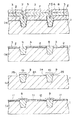
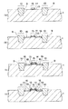
2,5,11,32,35,52,57,61,62 熱酸化膜
3,33,53,63 シリコン窒化膜
4,34,56,59 トレンチ(溝)
6,8,36,38,58 シリコン酸化膜
7,37 合わせ目部分
9 素子分離酸化膜
10,40,63 素子分離領域
12,60,65 多結晶シリコン膜
13,64 ゲート酸化膜
14,65 ゲート電極
15,66 ゲート部
16 低濃度n型不純物の拡散領域
18 側壁絶縁膜
19 高濃度n型不純物の拡散領域
20,69 層間絶縁膜
21,22,70,71,72 コンタクトホール
23,73 金属配線
39 欠損部
41 凹部
54 フォトレジスト
55 開口部
67,68 n型不純物の拡散領域
Claims (9)
- 半導体基板上に耐熱性絶縁膜を形成する第1の工程と、
前記耐熱性絶縁膜をパターニングする第2の工程と、
前記耐熱性絶縁膜の形状に倣って前記半導体基板の表面を選択的に除去し、該半導体基板に第1のトレンチを形成する第3の工程と、
前記第1のトレンチの内壁面を覆うように前記耐熱性絶縁膜上に第1の絶縁膜を形成し、前記第1のトレンチより幅の狭い第2のトレンチを形成する第4の工程と、
前記第2のトレンチを充填するように前記第1の絶縁膜上に該第1の絶縁膜より研磨速度選択比の大きい易酸化性膜を形成する第5の工程と、
前記易酸化性膜を前記第1の絶縁膜が露出するまで除去し、前記第2のトレンチ内のみに前記易酸化性膜を残す第6の工程と、
前記第2のトレンチ内に残された前記易酸化性膜を熱酸化し、該易酸化性膜の上面領域に第1の熱酸化膜を形成する第7の工程と、
表面に露出している第1の絶縁膜及び前記第1の熱酸化膜の一部を、前記耐熱性絶縁膜が露出するまで除去する第8の工程と、
前記第2のトレンチ内に残された前記易酸化性膜を再び熱酸化し、該易酸化性膜の上面領域に第2の熱酸化膜を形成する第9の工程と、
表面に露出している前記耐熱性絶縁膜を除去する第10の工程とを有することを特徴とする半導体装置の製造方法。 - 前記易酸化性膜がポリシリコン膜であることを特徴とする請求項1に記載の半導体装置の製造方法。
- 前記第1の絶縁膜がシリコン酸化膜であることを特徴とする請求項1に記載の半導体装置の製造方法。
- 前記第1の工程の前に、前記半導体基板上にパッド絶縁膜を形成する第11の工程を更に含むと共に、前記第10の工程の後に、前記パッド絶縁膜を除去する第12の工程を更に含み、
前記第1の工程では前記半導体基板との間に前記パッド絶縁膜を介して前記耐熱性絶縁膜を形成し、前記第2の工程では前記耐熱性絶縁膜と共に前記パッド絶縁膜をパターニングすることを特徴とする請求項1に記載の半導体装置の製造方法。 - 前記第6の工程において前記易酸化性膜を化学機械研磨法により除去することを特徴とする請求項1に記載の半導体装置の製造方法。
- 前記第1の絶縁膜を化学機械研磨法のストッパとして用いることを特徴とする請求項5に記載の半導体装置の製造方法。
- 前記第1の絶縁膜に対する前記易酸化性膜の研磨速度選択比は20倍以上に設定されていることを特徴とする請求項1に記載の半導体装置の製造方法。
- 前記第1の熱酸化膜の膜厚は前記第1の絶縁膜の膜厚より大きく設定されていることを特徴とする請求項1に記載の半導体装置の製造方法。
- 前記第3の工程と前記第4の工程の間に、前記第1のトレンチの底面から側壁にかけての表面領域に第2の絶縁膜を形成する第13の工程を更に有することを特徴とする請求項1に記載の半導体装置の製造方法。
Priority Applications (1)
| Application Number | Priority Date | Filing Date | Title |
|---|---|---|---|
| JP2009042807A JP5073694B2 (ja) | 1997-06-13 | 2009-02-25 | 半導体装置の製造方法 |
Applications Claiming Priority (5)
| Application Number | Priority Date | Filing Date | Title |
|---|---|---|---|
| JP1997173113 | 1997-06-13 | ||
| JP17311397 | 1997-06-13 | ||
| JP19055197 | 1997-07-01 | ||
| JP1997190551 | 1997-07-01 | ||
| JP2009042807A JP5073694B2 (ja) | 1997-06-13 | 2009-02-25 | 半導体装置の製造方法 |
Related Parent Applications (1)
| Application Number | Title | Priority Date | Filing Date |
|---|---|---|---|
| JP16726498A Division JPH1174343A (ja) | 1997-06-13 | 1998-06-15 | 半導体装置及びその製造方法 |
Publications (2)
| Publication Number | Publication Date |
|---|---|
| JP2009124178A JP2009124178A (ja) | 2009-06-04 |
| JP5073694B2 true JP5073694B2 (ja) | 2012-11-14 |
Family
ID=40815926
Family Applications (2)
| Application Number | Title | Priority Date | Filing Date |
|---|---|---|---|
| JP2009042807A Expired - Lifetime JP5073694B2 (ja) | 1997-06-13 | 2009-02-25 | 半導体装置の製造方法 |
| JP2009042934A Expired - Lifetime JP5073695B2 (ja) | 1997-06-13 | 2009-02-25 | 半導体装置の製造方法 |
Family Applications After (1)
| Application Number | Title | Priority Date | Filing Date |
|---|---|---|---|
| JP2009042934A Expired - Lifetime JP5073695B2 (ja) | 1997-06-13 | 2009-02-25 | 半導体装置の製造方法 |
Country Status (1)
| Country | Link |
|---|---|
| JP (2) | JP5073694B2 (ja) |
Family Cites Families (8)
| Publication number | Priority date | Publication date | Assignee | Title |
|---|---|---|---|---|
| JPH02125443A (ja) * | 1988-11-04 | 1990-05-14 | Fujitsu Ltd | 半導体装置とその製造方法 |
| JP2688090B2 (ja) * | 1989-11-10 | 1997-12-08 | シャープ株式会社 | 半導体装置の製造方法 |
| JP3311044B2 (ja) * | 1992-10-27 | 2002-08-05 | 株式会社東芝 | 半導体装置の製造方法 |
| JPH06232248A (ja) * | 1993-02-01 | 1994-08-19 | Fujitsu Ltd | 半導体装置の製造方法 |
| JPH07273330A (ja) * | 1994-03-31 | 1995-10-20 | Toshiba Corp | 半導体装置及びその製造方法 |
| JPH0817909A (ja) * | 1994-06-28 | 1996-01-19 | Canon Inc | 半導体装置の製造方法 |
| JPH08330410A (ja) * | 1995-05-31 | 1996-12-13 | Sony Corp | 素子分離方法、素子分離構造、及び半導体装置 |
| JPH0945761A (ja) * | 1995-07-31 | 1997-02-14 | Toshiba Corp | 半導体装置の製造方法 |
-
2009
- 2009-02-25 JP JP2009042807A patent/JP5073694B2/ja not_active Expired - Lifetime
- 2009-02-25 JP JP2009042934A patent/JP5073695B2/ja not_active Expired - Lifetime
Also Published As
| Publication number | Publication date |
|---|---|
| JP5073695B2 (ja) | 2012-11-14 |
| JP2009124179A (ja) | 2009-06-04 |
| JP2009124178A (ja) | 2009-06-04 |
Similar Documents
| Publication | Publication Date | Title |
|---|---|---|
| US7858490B2 (en) | Semiconductor device having dual-STI and manufacturing method thereof | |
| US6798038B2 (en) | Manufacturing method of semiconductor device with filling insulating film into trench | |
| JP3604818B2 (ja) | 半導体装置の製造方法 | |
| CN100550340C (zh) | 制造半导体器件的方法 | |
| JP2012109595A (ja) | 半導体装置の製造方法 | |
| TWI389249B (zh) | Semiconductor device and manufacturing method thereof | |
| US6020622A (en) | Trench isolation for semiconductor device with lateral projections above substrate | |
| JP3670455B2 (ja) | 浅いトレンチ分離法を用いて製造された半導体装置及びその製造方法 | |
| JP2012028805A (ja) | 半導体装置の製造方法 | |
| US20100155905A1 (en) | Semiconductor device and its manufacturing method | |
| KR100636031B1 (ko) | 불휘발성 메모리 장치의 제조 방법. | |
| JP5073694B2 (ja) | 半導体装置の製造方法 | |
| JP3127893B2 (ja) | 半導体装置および半導体装置の製造方法 | |
| US6265284B1 (en) | Method of manufacturing a trench isolation region in a semiconductor device | |
| JPH1174343A (ja) | 半導体装置及びその製造方法 | |
| JP5288814B2 (ja) | 半導体装置の製造方法 | |
| JP2004296754A (ja) | 半導体装置および半導体装置の製造方法 | |
| US20040082141A1 (en) | Method of fabricating a semiconductor device having trenches | |
| US6846721B2 (en) | Manufacturing method of semiconductor device | |
| JPH10242264A (ja) | 半導体装置の製造方法 | |
| KR100639182B1 (ko) | 반도체장치의 소자격리방법 | |
| KR100781872B1 (ko) | 소자분리막 형성 방법 | |
| KR100376868B1 (ko) | 반도체장치의 제조방법 | |
| KR100478265B1 (ko) | 반도체 제조 공정에서의 모트 마스크 디자인 방법 | |
| JP3409134B2 (ja) | 半導体装置の製造方法 |
Legal Events
| Date | Code | Title | Description |
|---|---|---|---|
| A621 | Written request for application examination |
Free format text: JAPANESE INTERMEDIATE CODE: A621 Effective date: 20090226 |
|
| RD02 | Notification of acceptance of power of attorney |
Free format text: JAPANESE INTERMEDIATE CODE: A7422 Effective date: 20100104 |
|
| A977 | Report on retrieval |
Free format text: JAPANESE INTERMEDIATE CODE: A971007 Effective date: 20120308 |
|
| A131 | Notification of reasons for refusal |
Free format text: JAPANESE INTERMEDIATE CODE: A131 Effective date: 20120321 |
|
| A521 | Written amendment |
Free format text: JAPANESE INTERMEDIATE CODE: A523 Effective date: 20120516 |
|
| TRDD | Decision of grant or rejection written | ||
| A01 | Written decision to grant a patent or to grant a registration (utility model) |
Free format text: JAPANESE INTERMEDIATE CODE: A01 Effective date: 20120814 |
|
| A01 | Written decision to grant a patent or to grant a registration (utility model) |
Free format text: JAPANESE INTERMEDIATE CODE: A01 |
|
| A61 | First payment of annual fees (during grant procedure) |
Free format text: JAPANESE INTERMEDIATE CODE: A61 Effective date: 20120822 |
|
| R150 | Certificate of patent or registration of utility model |
Free format text: JAPANESE INTERMEDIATE CODE: R150 |
|
| FPAY | Renewal fee payment (event date is renewal date of database) |
Free format text: PAYMENT UNTIL: 20150831 Year of fee payment: 3 |
|
| R250 | Receipt of annual fees |
Free format text: JAPANESE INTERMEDIATE CODE: R250 |
|
| R250 | Receipt of annual fees |
Free format text: JAPANESE INTERMEDIATE CODE: R250 |
|
| R250 | Receipt of annual fees |
Free format text: JAPANESE INTERMEDIATE CODE: R250 |
|
| EXPY | Cancellation because of completion of term |