KR20130130879A - 반도체 장치 제작방법 - Google Patents
반도체 장치 제작방법 Download PDFInfo
- Publication number
- KR20130130879A KR20130130879A KR1020137030134A KR20137030134A KR20130130879A KR 20130130879 A KR20130130879 A KR 20130130879A KR 1020137030134 A KR1020137030134 A KR 1020137030134A KR 20137030134 A KR20137030134 A KR 20137030134A KR 20130130879 A KR20130130879 A KR 20130130879A
- Authority
- KR
- South Korea
- Prior art keywords
- film
- oxide semiconductor
- insulating film
- electrode
- conductive film
- Prior art date
- Legal status (The legal status is an assumption and is not a legal conclusion. Google has not performed a legal analysis and makes no representation as to the accuracy of the status listed.)
- Ceased
Links
- 239000004065 semiconductor Substances 0.000 title claims abstract description 501
- 238000000034 method Methods 0.000 title claims description 83
- 238000004519 manufacturing process Methods 0.000 title abstract description 51
- 239000001257 hydrogen Substances 0.000 claims abstract description 68
- 229910052739 hydrogen Inorganic materials 0.000 claims abstract description 68
- 239000010936 titanium Substances 0.000 claims abstract description 56
- RTAQQCXQSZGOHL-UHFFFAOYSA-N Titanium Chemical compound [Ti] RTAQQCXQSZGOHL-UHFFFAOYSA-N 0.000 claims abstract description 55
- 229910052719 titanium Inorganic materials 0.000 claims abstract description 55
- UFHFLCQGNIYNRP-UHFFFAOYSA-N Hydrogen Chemical compound [H][H] UFHFLCQGNIYNRP-UHFFFAOYSA-N 0.000 claims abstract description 52
- 229910052721 tungsten Inorganic materials 0.000 claims abstract description 29
- 239000010937 tungsten Substances 0.000 claims abstract description 29
- ZOKXTWBITQBERF-UHFFFAOYSA-N Molybdenum Chemical compound [Mo] ZOKXTWBITQBERF-UHFFFAOYSA-N 0.000 claims abstract description 27
- 229910052750 molybdenum Inorganic materials 0.000 claims abstract description 27
- 239000011733 molybdenum Substances 0.000 claims abstract description 27
- WFKWXMTUELFFGS-UHFFFAOYSA-N tungsten Chemical compound [W] WFKWXMTUELFFGS-UHFFFAOYSA-N 0.000 claims abstract description 27
- 239000000758 substrate Substances 0.000 claims description 97
- IJGRMHOSHXDMSA-UHFFFAOYSA-N Atomic nitrogen Chemical compound N#N IJGRMHOSHXDMSA-UHFFFAOYSA-N 0.000 claims description 88
- 239000004973 liquid crystal related substance Substances 0.000 claims description 53
- VYPSYNLAJGMNEJ-UHFFFAOYSA-N Silicium dioxide Chemical compound O=[Si]=O VYPSYNLAJGMNEJ-UHFFFAOYSA-N 0.000 claims description 46
- 229910052814 silicon oxide Inorganic materials 0.000 claims description 45
- 229910052757 nitrogen Inorganic materials 0.000 claims description 39
- 229910052581 Si3N4 Inorganic materials 0.000 claims description 38
- 229910052751 metal Inorganic materials 0.000 claims description 38
- HQVNEWCFYHHQES-UHFFFAOYSA-N silicon nitride Chemical compound N12[Si]34N5[Si]62N3[Si]51N64 HQVNEWCFYHHQES-UHFFFAOYSA-N 0.000 claims description 38
- 239000002184 metal Substances 0.000 claims description 37
- XUIMIQQOPSSXEZ-UHFFFAOYSA-N Silicon Chemical compound [Si] XUIMIQQOPSSXEZ-UHFFFAOYSA-N 0.000 claims description 30
- 229910052710 silicon Inorganic materials 0.000 claims description 30
- 239000010703 silicon Substances 0.000 claims description 30
- QVGXLLKOCUKJST-UHFFFAOYSA-N atomic oxygen Chemical compound [O] QVGXLLKOCUKJST-UHFFFAOYSA-N 0.000 claims description 22
- 239000001301 oxygen Substances 0.000 claims description 22
- 229910052760 oxygen Inorganic materials 0.000 claims description 22
- 229910007541 Zn O Inorganic materials 0.000 claims description 15
- RYGMFSIKBFXOCR-UHFFFAOYSA-N Copper Chemical compound [Cu] RYGMFSIKBFXOCR-UHFFFAOYSA-N 0.000 claims description 7
- 229910052802 copper Inorganic materials 0.000 claims description 7
- 239000010949 copper Substances 0.000 claims description 7
- 229910052738 indium Inorganic materials 0.000 claims description 6
- APFVFJFRJDLVQX-UHFFFAOYSA-N indium atom Chemical compound [In] APFVFJFRJDLVQX-UHFFFAOYSA-N 0.000 claims description 5
- 125000006850 spacer group Chemical group 0.000 claims description 4
- 239000013078 crystal Substances 0.000 claims description 3
- 229910019092 Mg-O Inorganic materials 0.000 claims description 2
- 229910019395 Mg—O Inorganic materials 0.000 claims description 2
- 239000010408 film Substances 0.000 abstract description 1260
- 238000005530 etching Methods 0.000 abstract description 55
- 239000010409 thin film Substances 0.000 abstract description 50
- 238000010438 heat treatment Methods 0.000 description 107
- 239000010410 layer Substances 0.000 description 83
- 239000012535 impurity Substances 0.000 description 81
- 239000012298 atmosphere Substances 0.000 description 79
- 239000000463 material Substances 0.000 description 79
- 238000004544 sputter deposition Methods 0.000 description 72
- 229910052782 aluminium Inorganic materials 0.000 description 59
- NBIIXXVUZAFLBC-UHFFFAOYSA-N Phosphoric acid Chemical compound OP(O)(O)=O NBIIXXVUZAFLBC-UHFFFAOYSA-N 0.000 description 56
- XAGFODPZIPBFFR-UHFFFAOYSA-N aluminium Chemical compound [Al] XAGFODPZIPBFFR-UHFFFAOYSA-N 0.000 description 56
- XKRFYHLGVUSROY-UHFFFAOYSA-N Argon Chemical compound [Ar] XKRFYHLGVUSROY-UHFFFAOYSA-N 0.000 description 52
- 239000000956 alloy Substances 0.000 description 44
- 239000007789 gas Substances 0.000 description 43
- 229910045601 alloy Inorganic materials 0.000 description 42
- 230000004888 barrier function Effects 0.000 description 42
- 239000000243 solution Substances 0.000 description 42
- XLYOFNOQVPJJNP-UHFFFAOYSA-N water Substances O XLYOFNOQVPJJNP-UHFFFAOYSA-N 0.000 description 40
- QGZKDVFQNNGYKY-UHFFFAOYSA-N Ammonia Chemical compound N QGZKDVFQNNGYKY-UHFFFAOYSA-N 0.000 description 39
- 230000015572 biosynthetic process Effects 0.000 description 37
- XLOMVQKBTHCTTD-UHFFFAOYSA-N Zinc monoxide Chemical compound [Zn]=O XLOMVQKBTHCTTD-UHFFFAOYSA-N 0.000 description 29
- 229910000147 aluminium phosphate Inorganic materials 0.000 description 28
- MHAJPDPJQMAIIY-UHFFFAOYSA-N Hydrogen peroxide Chemical compound OO MHAJPDPJQMAIIY-UHFFFAOYSA-N 0.000 description 27
- 239000007769 metal material Substances 0.000 description 27
- 230000008569 process Effects 0.000 description 27
- 229910052786 argon Inorganic materials 0.000 description 26
- 239000000460 chlorine Substances 0.000 description 26
- QTBSBXVTEAMEQO-UHFFFAOYSA-N acetic acid Substances CC(O)=O QTBSBXVTEAMEQO-UHFFFAOYSA-N 0.000 description 25
- 239000011261 inert gas Substances 0.000 description 25
- 239000003094 microcapsule Substances 0.000 description 23
- 150000002736 metal compounds Chemical class 0.000 description 22
- 239000001307 helium Substances 0.000 description 21
- 229910052734 helium Inorganic materials 0.000 description 21
- SWQJXJOGLNCZEY-UHFFFAOYSA-N helium atom Chemical compound [He] SWQJXJOGLNCZEY-UHFFFAOYSA-N 0.000 description 21
- PMHQVHHXPFUNSP-UHFFFAOYSA-M copper(1+);methylsulfanylmethane;bromide Chemical compound Br[Cu].CSC PMHQVHHXPFUNSP-UHFFFAOYSA-M 0.000 description 20
- 230000006866 deterioration Effects 0.000 description 19
- 238000010586 diagram Methods 0.000 description 17
- 239000011521 glass Substances 0.000 description 17
- 229910021529 ammonia Inorganic materials 0.000 description 16
- 239000003990 capacitor Substances 0.000 description 16
- 150000002431 hydrogen Chemical class 0.000 description 16
- 238000000059 patterning Methods 0.000 description 16
- ZAMOUSCENKQFHK-UHFFFAOYSA-N Chlorine atom Chemical compound [Cl] ZAMOUSCENKQFHK-UHFFFAOYSA-N 0.000 description 15
- 229910052801 chlorine Inorganic materials 0.000 description 15
- -1 tungsten nitride Chemical class 0.000 description 15
- VHUUQVKOLVNVRT-UHFFFAOYSA-N Ammonium hydroxide Chemical compound [NH4+].[OH-] VHUUQVKOLVNVRT-UHFFFAOYSA-N 0.000 description 14
- 235000011114 ammonium hydroxide Nutrition 0.000 description 14
- 238000001039 wet etching Methods 0.000 description 13
- 239000011787 zinc oxide Substances 0.000 description 13
- 238000001312 dry etching Methods 0.000 description 12
- 230000006870 function Effects 0.000 description 12
- 239000000049 pigment Substances 0.000 description 12
- 230000001681 protective effect Effects 0.000 description 12
- 239000011347 resin Substances 0.000 description 12
- 229920005989 resin Polymers 0.000 description 12
- 239000002356 single layer Substances 0.000 description 12
- GRYLNZFGIOXLOG-UHFFFAOYSA-N Nitric acid Chemical compound O[N+]([O-])=O GRYLNZFGIOXLOG-UHFFFAOYSA-N 0.000 description 11
- NRTOMJZYCJJWKI-UHFFFAOYSA-N Titanium nitride Chemical compound [Ti]#N NRTOMJZYCJJWKI-UHFFFAOYSA-N 0.000 description 11
- 239000011159 matrix material Substances 0.000 description 11
- 229910017604 nitric acid Inorganic materials 0.000 description 11
- FAQYAMRNWDIXMY-UHFFFAOYSA-N trichloroborane Chemical compound ClB(Cl)Cl FAQYAMRNWDIXMY-UHFFFAOYSA-N 0.000 description 11
- 239000002253 acid Substances 0.000 description 10
- 239000007864 aqueous solution Substances 0.000 description 10
- 230000005669 field effect Effects 0.000 description 10
- 239000000203 mixture Substances 0.000 description 10
- 238000000206 photolithography Methods 0.000 description 10
- 239000000126 substance Substances 0.000 description 10
- 239000012463 white pigment Substances 0.000 description 10
- VYZAMTAEIAYCRO-UHFFFAOYSA-N Chromium Chemical compound [Cr] VYZAMTAEIAYCRO-UHFFFAOYSA-N 0.000 description 9
- 229910052804 chromium Inorganic materials 0.000 description 9
- 239000011651 chromium Substances 0.000 description 9
- 239000011777 magnesium Substances 0.000 description 9
- 229910044991 metal oxide Inorganic materials 0.000 description 9
- 150000004706 metal oxides Chemical class 0.000 description 9
- 238000002156 mixing Methods 0.000 description 9
- 239000012071 phase Substances 0.000 description 9
- 229910052779 Neodymium Inorganic materials 0.000 description 8
- 239000012300 argon atmosphere Substances 0.000 description 8
- 238000009792 diffusion process Methods 0.000 description 8
- AMGQUBHHOARCQH-UHFFFAOYSA-N indium;oxotin Chemical compound [In].[Sn]=O AMGQUBHHOARCQH-UHFFFAOYSA-N 0.000 description 8
- QEFYFXOXNSNQGX-UHFFFAOYSA-N neodymium atom Chemical compound [Nd] QEFYFXOXNSNQGX-UHFFFAOYSA-N 0.000 description 8
- 239000004020 conductor Substances 0.000 description 7
- 229910003437 indium oxide Inorganic materials 0.000 description 7
- PJXISJQVUVHSOJ-UHFFFAOYSA-N indium(iii) oxide Chemical compound [O-2].[O-2].[O-2].[In+3].[In+3] PJXISJQVUVHSOJ-UHFFFAOYSA-N 0.000 description 7
- 229910052749 magnesium Inorganic materials 0.000 description 7
- 150000002739 metals Chemical class 0.000 description 7
- 229910052754 neon Inorganic materials 0.000 description 7
- GKAOGPIIYCISHV-UHFFFAOYSA-N neon atom Chemical compound [Ne] GKAOGPIIYCISHV-UHFFFAOYSA-N 0.000 description 7
- 238000012545 processing Methods 0.000 description 7
- 238000003860 storage Methods 0.000 description 7
- GQPLMRYTRLFLPF-UHFFFAOYSA-N Nitrous Oxide Chemical compound [O-][N+]#N GQPLMRYTRLFLPF-UHFFFAOYSA-N 0.000 description 6
- 229910052783 alkali metal Inorganic materials 0.000 description 6
- 150000001340 alkali metals Chemical class 0.000 description 6
- 238000002347 injection Methods 0.000 description 6
- 239000007924 injection Substances 0.000 description 6
- 238000004151 rapid thermal annealing Methods 0.000 description 6
- 229910052706 scandium Inorganic materials 0.000 description 6
- SIXSYDAISGFNSX-UHFFFAOYSA-N scandium atom Chemical compound [Sc] SIXSYDAISGFNSX-UHFFFAOYSA-N 0.000 description 6
- 229910052715 tantalum Inorganic materials 0.000 description 6
- GUVRBAGPIYLISA-UHFFFAOYSA-N tantalum atom Chemical compound [Ta] GUVRBAGPIYLISA-UHFFFAOYSA-N 0.000 description 6
- MYMOFIZGZYHOMD-UHFFFAOYSA-N Dioxygen Chemical compound O=O MYMOFIZGZYHOMD-UHFFFAOYSA-N 0.000 description 5
- 239000002585 base Substances 0.000 description 5
- 229910001873 dinitrogen Inorganic materials 0.000 description 5
- 229910001882 dioxygen Inorganic materials 0.000 description 5
- 239000000428 dust Substances 0.000 description 5
- 238000001307 laser spectroscopy Methods 0.000 description 5
- 239000012299 nitrogen atmosphere Substances 0.000 description 5
- 229910052756 noble gas Inorganic materials 0.000 description 5
- 238000005268 plasma chemical vapour deposition Methods 0.000 description 5
- 239000011701 zinc Substances 0.000 description 5
- 229910005191 Ga 2 O 3 Inorganic materials 0.000 description 4
- PXHVJJICTQNCMI-UHFFFAOYSA-N Nickel Chemical compound [Ni] PXHVJJICTQNCMI-UHFFFAOYSA-N 0.000 description 4
- 239000004696 Poly ether ether ketone Substances 0.000 description 4
- 239000004642 Polyimide Substances 0.000 description 4
- 229910052791 calcium Inorganic materials 0.000 description 4
- 239000011575 calcium Substances 0.000 description 4
- 230000001747 exhibiting effect Effects 0.000 description 4
- 239000010419 fine particle Substances 0.000 description 4
- 229910052733 gallium Inorganic materials 0.000 description 4
- 229910001385 heavy metal Inorganic materials 0.000 description 4
- 239000007788 liquid Substances 0.000 description 4
- 229910052744 lithium Inorganic materials 0.000 description 4
- 239000002609 medium Substances 0.000 description 4
- 238000005192 partition Methods 0.000 description 4
- BASFCYQUMIYNBI-UHFFFAOYSA-N platinum Chemical compound [Pt] BASFCYQUMIYNBI-UHFFFAOYSA-N 0.000 description 4
- 229920002492 poly(sulfone) Polymers 0.000 description 4
- 229920001230 polyarylate Polymers 0.000 description 4
- 229920001707 polybutylene terephthalate Polymers 0.000 description 4
- 229920002530 polyetherether ketone Polymers 0.000 description 4
- 229920001721 polyimide Polymers 0.000 description 4
- 230000009467 reduction Effects 0.000 description 4
- 238000005070 sampling Methods 0.000 description 4
- 229910052709 silver Inorganic materials 0.000 description 4
- 229910052725 zinc Inorganic materials 0.000 description 4
- 229920000178 Acrylic resin Polymers 0.000 description 3
- 239000004925 Acrylic resin Substances 0.000 description 3
- 239000004986 Cholesteric liquid crystals (ChLC) Substances 0.000 description 3
- FYYHWMGAXLPEAU-UHFFFAOYSA-N Magnesium Chemical compound [Mg] FYYHWMGAXLPEAU-UHFFFAOYSA-N 0.000 description 3
- MUBZPKHOEPUJKR-UHFFFAOYSA-N Oxalic acid Chemical compound OC(=O)C(O)=O MUBZPKHOEPUJKR-UHFFFAOYSA-N 0.000 description 3
- HCHKCACWOHOZIP-UHFFFAOYSA-N Zinc Chemical compound [Zn] HCHKCACWOHOZIP-UHFFFAOYSA-N 0.000 description 3
- AZWHFTKIBIQKCA-UHFFFAOYSA-N [Sn+2]=O.[O-2].[In+3] Chemical compound [Sn+2]=O.[O-2].[In+3] AZWHFTKIBIQKCA-UHFFFAOYSA-N 0.000 description 3
- 229910021417 amorphous silicon Inorganic materials 0.000 description 3
- 230000001413 cellular effect Effects 0.000 description 3
- KRKNYBCHXYNGOX-UHFFFAOYSA-N citric acid Chemical compound OC(=O)CC(O)(C(O)=O)CC(O)=O KRKNYBCHXYNGOX-UHFFFAOYSA-N 0.000 description 3
- 150000001875 compounds Chemical class 0.000 description 3
- 238000003795 desorption Methods 0.000 description 3
- 229910010272 inorganic material Inorganic materials 0.000 description 3
- 239000011147 inorganic material Substances 0.000 description 3
- 150000004767 nitrides Chemical class 0.000 description 3
- 229960001730 nitrous oxide Drugs 0.000 description 3
- 229920003023 plastic Polymers 0.000 description 3
- 239000004033 plastic Substances 0.000 description 3
- 229920000139 polyethylene terephthalate Polymers 0.000 description 3
- 239000005020 polyethylene terephthalate Substances 0.000 description 3
- 239000003566 sealing material Substances 0.000 description 3
- TXEYQDLBPFQVAA-UHFFFAOYSA-N tetrafluoromethane Chemical compound FC(F)(F)F TXEYQDLBPFQVAA-UHFFFAOYSA-N 0.000 description 3
- YVTHLONGBIQYBO-UHFFFAOYSA-N zinc indium(3+) oxygen(2-) Chemical compound [O--].[Zn++].[In+3] YVTHLONGBIQYBO-UHFFFAOYSA-N 0.000 description 3
- UWCWUCKPEYNDNV-LBPRGKRZSA-N 2,6-dimethyl-n-[[(2s)-pyrrolidin-2-yl]methyl]aniline Chemical compound CC1=CC=CC(C)=C1NC[C@H]1NCCC1 UWCWUCKPEYNDNV-LBPRGKRZSA-N 0.000 description 2
- OKTJSMMVPCPJKN-UHFFFAOYSA-N Carbon Chemical compound [C] OKTJSMMVPCPJKN-UHFFFAOYSA-N 0.000 description 2
- 229910052691 Erbium Inorganic materials 0.000 description 2
- XPDWGBQVDMORPB-UHFFFAOYSA-N Fluoroform Chemical compound FC(F)F XPDWGBQVDMORPB-UHFFFAOYSA-N 0.000 description 2
- GYHNNYVSQQEPJS-UHFFFAOYSA-N Gallium Chemical compound [Ga] GYHNNYVSQQEPJS-UHFFFAOYSA-N 0.000 description 2
- VEXZGXHMUGYJMC-UHFFFAOYSA-N Hydrochloric acid Chemical compound Cl VEXZGXHMUGYJMC-UHFFFAOYSA-N 0.000 description 2
- CPELXLSAUQHCOX-UHFFFAOYSA-N Hydrogen bromide Chemical compound Br CPELXLSAUQHCOX-UHFFFAOYSA-N 0.000 description 2
- 229920012266 Poly(ether sulfone) PES Polymers 0.000 description 2
- 239000004983 Polymer Dispersed Liquid Crystal Substances 0.000 description 2
- 239000004743 Polypropylene Substances 0.000 description 2
- BQCADISMDOOEFD-UHFFFAOYSA-N Silver Chemical compound [Ag] BQCADISMDOOEFD-UHFFFAOYSA-N 0.000 description 2
- GWEVSGVZZGPLCZ-UHFFFAOYSA-N Titan oxide Chemical compound O=[Ti]=O GWEVSGVZZGPLCZ-UHFFFAOYSA-N 0.000 description 2
- 229910052769 Ytterbium Inorganic materials 0.000 description 2
- XECAHXYUAAWDEL-UHFFFAOYSA-N acrylonitrile butadiene styrene Chemical compound C=CC=C.C=CC#N.C=CC1=CC=CC=C1 XECAHXYUAAWDEL-UHFFFAOYSA-N 0.000 description 2
- 239000004676 acrylonitrile butadiene styrene Substances 0.000 description 2
- 229920000122 acrylonitrile butadiene styrene Polymers 0.000 description 2
- 229910052784 alkaline earth metal Inorganic materials 0.000 description 2
- 150000001342 alkaline earth metals Chemical class 0.000 description 2
- 230000008901 benefit Effects 0.000 description 2
- 229910052792 caesium Inorganic materials 0.000 description 2
- 239000006229 carbon black Substances 0.000 description 2
- 238000004140 cleaning Methods 0.000 description 2
- 230000006378 damage Effects 0.000 description 2
- 230000018044 dehydration Effects 0.000 description 2
- 238000006297 dehydration reaction Methods 0.000 description 2
- 238000006356 dehydrogenation reaction Methods 0.000 description 2
- 238000000151 deposition Methods 0.000 description 2
- JAONJTDQXUSBGG-UHFFFAOYSA-N dialuminum;dizinc;oxygen(2-) Chemical compound [O-2].[O-2].[O-2].[O-2].[O-2].[Al+3].[Al+3].[Zn+2].[Zn+2] JAONJTDQXUSBGG-UHFFFAOYSA-N 0.000 description 2
- AJNVQOSZGJRYEI-UHFFFAOYSA-N digallium;oxygen(2-) Chemical compound [O-2].[O-2].[O-2].[Ga+3].[Ga+3] AJNVQOSZGJRYEI-UHFFFAOYSA-N 0.000 description 2
- 238000007599 discharging Methods 0.000 description 2
- 239000006185 dispersion Substances 0.000 description 2
- 238000009826 distribution Methods 0.000 description 2
- 238000001035 drying Methods 0.000 description 2
- 230000000694 effects Effects 0.000 description 2
- 230000008030 elimination Effects 0.000 description 2
- 238000003379 elimination reaction Methods 0.000 description 2
- 239000004744 fabric Substances 0.000 description 2
- 239000000945 filler Substances 0.000 description 2
- 238000007667 floating Methods 0.000 description 2
- 229910001195 gallium oxide Inorganic materials 0.000 description 2
- 238000009616 inductively coupled plasma Methods 0.000 description 2
- 230000007257 malfunction Effects 0.000 description 2
- 238000005259 measurement Methods 0.000 description 2
- 229910052759 nickel Inorganic materials 0.000 description 2
- 239000001272 nitrous oxide Substances 0.000 description 2
- 230000003287 optical effect Effects 0.000 description 2
- 239000011368 organic material Substances 0.000 description 2
- 230000003647 oxidation Effects 0.000 description 2
- 238000007254 oxidation reaction Methods 0.000 description 2
- TWNQGVIAIRXVLR-UHFFFAOYSA-N oxo(oxoalumanyloxy)alumane Chemical compound O=[Al]O[Al]=O TWNQGVIAIRXVLR-UHFFFAOYSA-N 0.000 description 2
- BPUBBGLMJRNUCC-UHFFFAOYSA-N oxygen(2-);tantalum(5+) Chemical compound [O-2].[O-2].[O-2].[O-2].[O-2].[Ta+5].[Ta+5] BPUBBGLMJRNUCC-UHFFFAOYSA-N 0.000 description 2
- 238000001020 plasma etching Methods 0.000 description 2
- 229910052697 platinum Inorganic materials 0.000 description 2
- 239000004417 polycarbonate Substances 0.000 description 2
- 229920000515 polycarbonate Polymers 0.000 description 2
- 229910021420 polycrystalline silicon Inorganic materials 0.000 description 2
- 239000011112 polyethylene naphthalate Substances 0.000 description 2
- 229920001155 polypropylene Polymers 0.000 description 2
- 229920005591 polysilicon Polymers 0.000 description 2
- 229920002689 polyvinyl acetate Polymers 0.000 description 2
- 239000011118 polyvinyl acetate Substances 0.000 description 2
- 229920000915 polyvinyl chloride Polymers 0.000 description 2
- 239000004800 polyvinyl chloride Substances 0.000 description 2
- 229910052761 rare earth metal Inorganic materials 0.000 description 2
- 150000002910 rare earth metals Chemical class 0.000 description 2
- 239000003870 refractory metal Substances 0.000 description 2
- 239000004332 silver Substances 0.000 description 2
- 229910052712 strontium Inorganic materials 0.000 description 2
- 229920003002 synthetic resin Polymers 0.000 description 2
- 239000000057 synthetic resin Substances 0.000 description 2
- MZLGASXMSKOWSE-UHFFFAOYSA-N tantalum nitride Chemical compound [Ta]#N MZLGASXMSKOWSE-UHFFFAOYSA-N 0.000 description 2
- 229910001936 tantalum oxide Inorganic materials 0.000 description 2
- 239000013077 target material Substances 0.000 description 2
- VZGDMQKNWNREIO-UHFFFAOYSA-N tetrachloromethane Chemical compound ClC(Cl)(Cl)Cl VZGDMQKNWNREIO-UHFFFAOYSA-N 0.000 description 2
- OGIDPMRJRNCKJF-UHFFFAOYSA-N titanium oxide Inorganic materials [Ti]=O OGIDPMRJRNCKJF-UHFFFAOYSA-N 0.000 description 2
- 238000001771 vacuum deposition Methods 0.000 description 2
- OYQCBJZGELKKPM-UHFFFAOYSA-N zinc indium(3+) oxygen(2-) Chemical compound [O-2].[Zn+2].[O-2].[In+3] OYQCBJZGELKKPM-UHFFFAOYSA-N 0.000 description 2
- ZVWKZXLXHLZXLS-UHFFFAOYSA-N zirconium nitride Chemical compound [Zr]#N ZVWKZXLXHLZXLS-UHFFFAOYSA-N 0.000 description 2
- 101100392125 Caenorhabditis elegans gck-1 gene Proteins 0.000 description 1
- YCKRFDGAMUMZLT-UHFFFAOYSA-N Fluorine atom Chemical compound [F] YCKRFDGAMUMZLT-UHFFFAOYSA-N 0.000 description 1
- 102100022887 GTP-binding nuclear protein Ran Human genes 0.000 description 1
- 101000774835 Heteractis crispa PI-stichotoxin-Hcr2o Proteins 0.000 description 1
- 101000620756 Homo sapiens GTP-binding nuclear protein Ran Proteins 0.000 description 1
- 239000004677 Nylon Substances 0.000 description 1
- 238000006124 Pilkington process Methods 0.000 description 1
- 239000004372 Polyvinyl alcohol Substances 0.000 description 1
- 101100393821 Saccharomyces cerevisiae (strain ATCC 204508 / S288c) GSP2 gene Proteins 0.000 description 1
- BLRPTPMANUNPDV-UHFFFAOYSA-N Silane Chemical compound [SiH4] BLRPTPMANUNPDV-UHFFFAOYSA-N 0.000 description 1
- 229910020923 Sn-O Inorganic materials 0.000 description 1
- 229910006404 SnO 2 Inorganic materials 0.000 description 1
- ATJFFYVFTNAWJD-UHFFFAOYSA-N Tin Chemical compound [Sn] ATJFFYVFTNAWJD-UHFFFAOYSA-N 0.000 description 1
- 206010047571 Visual impairment Diseases 0.000 description 1
- 229910001297 Zn alloy Inorganic materials 0.000 description 1
- 239000000853 adhesive Substances 0.000 description 1
- 230000001070 adhesive effect Effects 0.000 description 1
- 239000005407 aluminoborosilicate glass Substances 0.000 description 1
- 239000005354 aluminosilicate glass Substances 0.000 description 1
- 238000000137 annealing Methods 0.000 description 1
- 229910052788 barium Inorganic materials 0.000 description 1
- DSAJWYNOEDNPEQ-UHFFFAOYSA-N barium atom Chemical compound [Ba] DSAJWYNOEDNPEQ-UHFFFAOYSA-N 0.000 description 1
- QVQLCTNNEUAWMS-UHFFFAOYSA-N barium oxide Chemical compound [Ba]=O QVQLCTNNEUAWMS-UHFFFAOYSA-N 0.000 description 1
- KGBXLFKZBHKPEV-UHFFFAOYSA-N boric acid Chemical compound OB(O)O KGBXLFKZBHKPEV-UHFFFAOYSA-N 0.000 description 1
- 239000004327 boric acid Substances 0.000 description 1
- 239000005388 borosilicate glass Substances 0.000 description 1
- 230000015556 catabolic process Effects 0.000 description 1
- 230000003197 catalytic effect Effects 0.000 description 1
- 239000000919 ceramic Substances 0.000 description 1
- 230000008859 change Effects 0.000 description 1
- 230000003098 cholesteric effect Effects 0.000 description 1
- 239000000470 constituent Substances 0.000 description 1
- 239000000110 cooling liquid Substances 0.000 description 1
- 230000007797 corrosion Effects 0.000 description 1
- 238000005260 corrosion Methods 0.000 description 1
- 238000002425 crystallisation Methods 0.000 description 1
- 230000008025 crystallization Effects 0.000 description 1
- 238000006731 degradation reaction Methods 0.000 description 1
- 230000003111 delayed effect Effects 0.000 description 1
- 230000008021 deposition Effects 0.000 description 1
- 230000002542 deteriorative effect Effects 0.000 description 1
- 238000007598 dipping method Methods 0.000 description 1
- 208000037265 diseases, disorders, signs and symptoms Diseases 0.000 description 1
- 239000002612 dispersion medium Substances 0.000 description 1
- 230000005684 electric field Effects 0.000 description 1
- 239000007772 electrode material Substances 0.000 description 1
- 238000001962 electrophoresis Methods 0.000 description 1
- 229910052731 fluorine Inorganic materials 0.000 description 1
- 239000011737 fluorine Substances 0.000 description 1
- 230000005525 hole transport Effects 0.000 description 1
- 229930195733 hydrocarbon Natural products 0.000 description 1
- 150000002430 hydrocarbons Chemical class 0.000 description 1
- 229910000042 hydrogen bromide Inorganic materials 0.000 description 1
- 238000007689 inspection Methods 0.000 description 1
- 239000012212 insulator Substances 0.000 description 1
- 238000003475 lamination Methods 0.000 description 1
- 238000001755 magnetron sputter deposition Methods 0.000 description 1
- 229910052748 manganese Inorganic materials 0.000 description 1
- 230000007246 mechanism Effects 0.000 description 1
- 230000004048 modification Effects 0.000 description 1
- 238000012986 modification Methods 0.000 description 1
- GVGCUCJTUSOZKP-UHFFFAOYSA-N nitrogen trifluoride Chemical compound FN(F)F GVGCUCJTUSOZKP-UHFFFAOYSA-N 0.000 description 1
- 235000013842 nitrous oxide Nutrition 0.000 description 1
- QGLKJKCYBOYXKC-UHFFFAOYSA-N nonaoxidotritungsten Chemical compound O=[W]1(=O)O[W](=O)(=O)O[W](=O)(=O)O1 QGLKJKCYBOYXKC-UHFFFAOYSA-N 0.000 description 1
- 229920001778 nylon Polymers 0.000 description 1
- 239000003921 oil Substances 0.000 description 1
- 150000007524 organic acids Chemical class 0.000 description 1
- 238000007500 overflow downdraw method Methods 0.000 description 1
- 235000006408 oxalic acid Nutrition 0.000 description 1
- 239000002245 particle Substances 0.000 description 1
- 238000009832 plasma treatment Methods 0.000 description 1
- 229920000728 polyester Polymers 0.000 description 1
- 239000002861 polymer material Substances 0.000 description 1
- 238000006116 polymerization reaction Methods 0.000 description 1
- 229920002451 polyvinyl alcohol Polymers 0.000 description 1
- 239000000843 powder Substances 0.000 description 1
- 238000003825 pressing Methods 0.000 description 1
- 238000005086 pumping Methods 0.000 description 1
- 239000010453 quartz Substances 0.000 description 1
- 238000005546 reactive sputtering Methods 0.000 description 1
- 238000004064 recycling Methods 0.000 description 1
- 230000004044 response Effects 0.000 description 1
- 230000000630 rising effect Effects 0.000 description 1
- 229910052594 sapphire Inorganic materials 0.000 description 1
- 239000010980 sapphire Substances 0.000 description 1
- 229910000077 silane Inorganic materials 0.000 description 1
- FDNAPBUWERUEDA-UHFFFAOYSA-N silicon tetrachloride Chemical compound Cl[Si](Cl)(Cl)Cl FDNAPBUWERUEDA-UHFFFAOYSA-N 0.000 description 1
- 238000009751 slip forming Methods 0.000 description 1
- 238000010583 slow cooling Methods 0.000 description 1
- 239000002904 solvent Substances 0.000 description 1
- SFZCNBIFKDRMGX-UHFFFAOYSA-N sulfur hexafluoride Chemical compound FS(F)(F)(F)(F)F SFZCNBIFKDRMGX-UHFFFAOYSA-N 0.000 description 1
- 238000002230 thermal chemical vapour deposition Methods 0.000 description 1
- XOLBLPGZBRYERU-UHFFFAOYSA-N tin dioxide Chemical compound O=[Sn]=O XOLBLPGZBRYERU-UHFFFAOYSA-N 0.000 description 1
- 229910001887 tin oxide Inorganic materials 0.000 description 1
- 238000012546 transfer Methods 0.000 description 1
- 230000007704 transition Effects 0.000 description 1
- 229910001930 tungsten oxide Inorganic materials 0.000 description 1
- 238000007740 vapor deposition Methods 0.000 description 1
- 238000001947 vapour-phase growth Methods 0.000 description 1
- 239000002699 waste material Substances 0.000 description 1
- 239000002351 wastewater Substances 0.000 description 1
Images


Classifications
-
- H—ELECTRICITY
- H10—SEMICONDUCTOR DEVICES; ELECTRIC SOLID-STATE DEVICES NOT OTHERWISE PROVIDED FOR
- H10D—INORGANIC ELECTRIC SEMICONDUCTOR DEVICES
- H10D30/00—Field-effect transistors [FET]
- H10D30/60—Insulated-gate field-effect transistors [IGFET]
- H10D30/67—Thin-film transistors [TFT]
- H10D30/6704—Thin-film transistors [TFT] having supplementary regions or layers in the thin films or in the insulated bulk substrates for controlling properties of the device
- H10D30/6713—Thin-film transistors [TFT] having supplementary regions or layers in the thin films or in the insulated bulk substrates for controlling properties of the device characterised by the properties of the source or drain regions, e.g. compositions or sectional shapes
-
- H—ELECTRICITY
- H10—SEMICONDUCTOR DEVICES; ELECTRIC SOLID-STATE DEVICES NOT OTHERWISE PROVIDED FOR
- H10D—INORGANIC ELECTRIC SEMICONDUCTOR DEVICES
- H10D30/00—Field-effect transistors [FET]
- H10D30/60—Insulated-gate field-effect transistors [IGFET]
- H10D30/67—Thin-film transistors [TFT]
- H10D30/674—Thin-film transistors [TFT] characterised by the active materials
- H10D30/6755—Oxide semiconductors, e.g. zinc oxide, copper aluminium oxide or cadmium stannate
-
- H—ELECTRICITY
- H10—SEMICONDUCTOR DEVICES; ELECTRIC SOLID-STATE DEVICES NOT OTHERWISE PROVIDED FOR
- H10D—INORGANIC ELECTRIC SEMICONDUCTOR DEVICES
- H10D30/00—Field-effect transistors [FET]
- H10D30/60—Insulated-gate field-effect transistors [IGFET]
- H10D30/67—Thin-film transistors [TFT]
- H10D30/6704—Thin-film transistors [TFT] having supplementary regions or layers in the thin films or in the insulated bulk substrates for controlling properties of the device
-
- H—ELECTRICITY
- H10—SEMICONDUCTOR DEVICES; ELECTRIC SOLID-STATE DEVICES NOT OTHERWISE PROVIDED FOR
- H10D—INORGANIC ELECTRIC SEMICONDUCTOR DEVICES
- H10D86/00—Integrated devices formed in or on insulating or conducting substrates, e.g. formed in silicon-on-insulator [SOI] substrates or on stainless steel or glass substrates
- H10D86/40—Integrated devices formed in or on insulating or conducting substrates, e.g. formed in silicon-on-insulator [SOI] substrates or on stainless steel or glass substrates characterised by multiple TFTs
- H10D86/421—Integrated devices formed in or on insulating or conducting substrates, e.g. formed in silicon-on-insulator [SOI] substrates or on stainless steel or glass substrates characterised by multiple TFTs having a particular composition, shape or crystalline structure of the active layer
- H10D86/423—Integrated devices formed in or on insulating or conducting substrates, e.g. formed in silicon-on-insulator [SOI] substrates or on stainless steel or glass substrates characterised by multiple TFTs having a particular composition, shape or crystalline structure of the active layer comprising semiconductor materials not belonging to the Group IV, e.g. InGaZnO
-
- H—ELECTRICITY
- H10—SEMICONDUCTOR DEVICES; ELECTRIC SOLID-STATE DEVICES NOT OTHERWISE PROVIDED FOR
- H10D—INORGANIC ELECTRIC SEMICONDUCTOR DEVICES
- H10D86/00—Integrated devices formed in or on insulating or conducting substrates, e.g. formed in silicon-on-insulator [SOI] substrates or on stainless steel or glass substrates
- H10D86/40—Integrated devices formed in or on insulating or conducting substrates, e.g. formed in silicon-on-insulator [SOI] substrates or on stainless steel or glass substrates characterised by multiple TFTs
- H10D86/60—Integrated devices formed in or on insulating or conducting substrates, e.g. formed in silicon-on-insulator [SOI] substrates or on stainless steel or glass substrates characterised by multiple TFTs wherein the TFTs are in active matrices
Landscapes
- Thin Film Transistor (AREA)
- Electrodes Of Semiconductors (AREA)
- Liquid Crystal (AREA)
- Electroluminescent Light Sources (AREA)
- Devices For Indicating Variable Information By Combining Individual Elements (AREA)
Abstract
Description
도 2는 박막 트랜지스터의 상면도이다.
도 3(A) 및 도 3(B)는 박막 트랜지스터의 단면도 및 상면도이다.
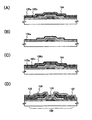
도 4(A) 내지 도 4(D)는 반도체 장치의 제작 방법을 나타내는 도이다.
도 5(A) 내지 도 5(D)는 반도체 장치의 제작 방법을 나타내는 도이다.
도 6(A) 내지 도 6(D)는 반도체 장치의 제작 방법을 나타내는 도이다.
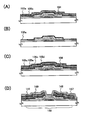
도 7(A) 내지 도 7(E)는 박막 트랜지스터의 단면도이다.
도 8은 박막 트랜지스터의 상면도이다.
도 9(A) 및 도 9(B)는 박막 트랜지스터의 단면도 및 상면도이다.
도 10(A) 내지 도 10(E)는 박막 트랜지스터의 단면도이다.
도 11은 박막 트랜지스터의 상면도이다.
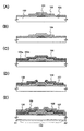
도 12(A) 내지 도 12(C)는 반도체 장치의 제작 방법을 나타내는 단면도이다.
도 13(A) 및 도 13(B)는 반도체 장치의 제작 방법을 나타내는 단면도이다.
도 14(A) 및 도 14(B)는 반도체 장치의 제작 방법을 나타내는 단면도이다.
도 15는 반도체 장치의 제작 방법을 나타내는 상면도이다.
도 16은 반도체 장치의 제작 방법을 나타내는 상면도이다.
도 17은 반도체 장치의 제작 방법을 나타내는 상면도이다.
도 18(A)는 전자 페이퍼의 상면도 및 도 18(B)는 전자 페이퍼의 단면도이다.단면도이다.
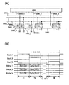
도 19(A) 및 도 19(B)는 반도체 표시장치의 블럭도이다.
도 20(A)는 신호선 구동회로의 구성을 설명하는 도이고 도 20(B)는 타이밍차트이다.
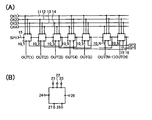
도 21(A) 및 도 21(B)는 시프트 레지스터의 구성을 나타내는 회로도이다.
도 22는 시프트 레지스터의 동작을 설명하는 타이밍 차트이다.
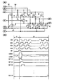
도 23은 액정표시장치의 단면도이다.
도 24는 액정표시장치의 모듈의 구성을 나타내는 도이다.
도 25(A) 내지 도 25(C)는 발광장치의 단면도이다.
도 26(A) 내지 도 26(E)는 반도체 장치를 이용한 전자기기의 도이다.
도 27은 산화물 반도체를 이용한 역스태거형 박막 트랜지스터의 종단면도이다.
도 28(A) 및 도 28(B)는 도 27에 나타내는 A-A' 단면에 있어서의 에너지 밴드도(모식도)이다.
도 29(A)는 게이트(G1)에 양의 전위(+VG)가 인가된 상태를 나타내고, 도 29(B)는 게이트(G1)에 음의 전위(-VG)가 인가된 상태를 나타내는 도이다.
도 30은 진공 준위와 금속의 일함수(φM), 산화물 반도체의 전자 친화력(χ)의 관계를 나타내는 도이다.
12 : 배선 13 : 배선
14 : 배선 15 : 배선
21 : 입력단자 22 : 입력단자
23 : 입력단자 24 : 입력단자
25 : 입력단자 26 : 출력단자
27 : 출력단자 31 : 트랜지스터
32 : 트랜지스터 33 : 트랜지스터
34 : 트랜지스터 35 : 트랜지스터
36 : 트랜지스터 37 : 트랜지스터
38 : 트랜지스터 39 : 트랜지스터
40 : 트랜지스터 41 : 트랜지스터
42 : 트랜지스터 43 : 트랜지스터
51 : 전원선 52 : 전원선
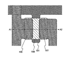
53 : 전원선 100 : 기판
101 : 게이트 전극 102 : 게이트 절연막
103 : 산화물 반도체막 104 : 산화물 반도체막
105a : 도전막 105b : 도전막
105c : 도전막 105d : 도전막
105e : 도전막 106 : 소스 전극
107 : 드레인 전극 108 : 산화물 반도체막
109 : 절연막 110 : 트랜지스터
111 : 백게이트 전극 112 : 절연막
120 : 박막 트랜지스터 126 : 소스 전극
127 : 드레인 전극 128 : 산화물 반도체막
129 : 절연막 130 : 박막 트랜지스터
136 : 소스 전극 137 : 드레인 전극
138 : 산화물 반도체막 139 : 절연막
140 : 박막 트랜지스터 146 : 소스 전극
147 : 드레인 전극 148 : 산화물 반도체막
149 : 절연막 300 : 기판
301 : 게이트 전극 302 : 게이트 절연막
303 : 산화물 반도체막 304 : 산화물 반도체막
305a : 도전막 305b : 도전막
306 : 소스 전극 307 : 드레인 전극
309 : 절연막 310 : 박막 트랜지스터
311 : 채널 보호막 312 : 백게이트 전극
313 : 절연막 400 : 기판
401 : 게이트 전극 402 : 게이트 절연막
403 : 산화물 반도체막 404 : 산화물 반도체막
405a : 도전막 405b : 도전막
406 : 소스 전극 407 : 드레인 전극
409 : 절연막 410 : 박막 트랜지스터
700 : 화소부 701 : 신호선 구동회로
702 : 주사선 구동회로 703 : 화소
704 : 트랜지스터 705 : 표시소자
706 : 유지용량 707 : 신호선
708 : 주사선 710 : 화소 전극
711 : 대향 전극 712 : 마이크로 캡슐
713 : 드레인 전극 714 : 수지
800 : 기판 801 : 게이트 전극
802 : 게이트 절연막 803 : 산화물 반도체막
804 : 산화물 반도체막 805 : 산화물 반도체막
806 : 도전막 806a : 도전막
806b : 도전막 807 : 소스 전극
808 : 드레인 전극 809 : 절연막
813 : 박막 트랜지스터 814 : 화소 전극
815 : 투명 도전막 816 : 투명 도전막
819 : 유지용량 820 : 단자
821 : 단자 822 : 용량 배선
1401 : 박막 트랜지스터 1402 : 게이트 전극
1403 : 게이트 절연막 1404 : 산화물 반도체막
1406a : 도전막 1406b : 도전막
1407 : 절연막 1408 : 절연막
1410 : 화소 전극 1411 : 배향막
1413 : 대향 전극 1414 : 배향막
1415 : 액정 1416 : 시일재
1417 : 스페이서 1420 : 기판
1601 : 액정패널 1602 : 확산판
1603 : 프리즘 시트 1604 : 확산판
1605 : 도광판 1606 : 반사판
1607 : 광원 1608 : 회로기판
1609 : FPC 1610 : FPC
5300 : 기판 5301 : 화소부
5302 : 주사선 구동회로 5303 : 주사선 구동회로
5304 : 신호선 구동회로 5305 : 타이밍 제어 회로
5601 : 시프트 레지스터 5602 : 샘플링 회로
5603 : 트랜지스터 5604 : 배선
5605 : 배선 6031 : 트랜지스터
6033 : 발광소자 6034 : 전극
6035 : 전계 발광층 6036 : 전극
6037 : 절연막 6038 : 격벽
6041 : 트랜지스터 6043 : 발광소자
6044 : 전극 6045 : 전계 발광층
6046 : 전극 6047 : 절연막
6048 : 격벽 6051 : 트랜지스터
6053 : 발광소자 6054 : 전극
6055 : 전계 발광층 6056 : 전극
6057 : 절연막 6058 : 격벽
7001 : 하우징 7002 : 표시부
7011 : 하우징 7012 : 표시부
7013 : 지지대 7021 : 하우징
7022 : 표시부 7031 : 하우징
7032 : 하우징 7033 : 표시부
7034 : 표시부 7035 : 마이크로폰
7036 : 스피커 7037 : 조작 키
7038 : 스타일러스 7041 : 하우징
7042 : 표시부 7043 : 음성 입력부
7044 : 음성 출력부 7045 : 조작 키
7046 : 수광부
Claims (14)
- 반도체 장치에 있어서,
기판 위에 있고, 구리를 포함하는 게이트 전극;
상기 게이트 전극 위에 있고, 질화 실리콘을 포함하는 제 1 절연막;
상기 제 1 절연막 위에 있고, 산화 실리콘을 포함하는 제 2 절연막;
상기 제 2 절연막 위에 있고, 인듐과 산소를 포함하는 산화물 반도체막;
상기 산화물 반도체막과 전기적으로 접속된 소스 전극;
상기 산화물 반도체막과 전기적으로 접속된 드레인 전극;
상기 산화물 반도체막, 상기 소스 전극, 및 상기 드레인 전극 위에 있고, 산화 실리콘을 포함하는 제 3 절연막;
상기 제 3 절연막 위에 있고, 질화 실리콘을 포함하는 제 4 절연막; 및
상기 제 4 절연막 위에 있고, 상기 소스 전극과 상기 드레인 전극 중 하나에 전기적으로 접속된 화소 전극을 포함하고,
상기 제 3 절연막은 상기 산화물 반도체막의 상부 표면과 접촉하고,
산화 실리콘을 포함하는 상기 제 2 절연막은 산화 실리콘을 포함하는 상기 제 3 절연막과 접촉하는, 반도체 장치. - 반도체 장치에 있어서,
기판 위에 있고, 구리를 포함하는 게이트 전극;
상기 게이트 전극 위에 있고, 질화 실리콘을 포함하는 제 1 절연막;
상기 제 1 절연막 위에 있고, 산질화 실리콘을 포함하는 제 2 절연막;
상기 제 2 절연막 위에 있고, 인듐과 산소를 포함하는 산화물 반도체막;
상기 산화물 반도체막과 전기적으로 접속된 소스 전극;
상기 산화물 반도체막과 전기적으로 접속된 드레인 전극;
상기 산화물 반도체막, 상기 소스 전극, 및 상기 드레인 전극 위에 있고, 산질화 실리콘을 포함하는 제 3 절연막;
상기 제 3 절연막 위에 있고, 질화 실리콘을 포함하는 제 4 절연막; 및
상기 제 4 절연막 위에 있고, 상기 소스 전극과 상기 드레인 전극 중 하나에 전기적으로 접속된 화소 전극을 포함하고,
상기 제 3 절연막은 상기 산화물 반도체막의 상부 표면과 접촉하는, 반도체 장치. - 제 1 항 또는 제 2 항에 있어서,
상기 산화물 반도체막은 In-Ga-Zn-O계 산화물 반도체를 포함하는, 반도체 장치. - 제 1 항 또는 제 2 항에 있어서,
상기 산화물 반도체막은 In-Sn-Ga-Zn-O계 산화물 반도체, In-Sn-Zn-O계 산화물 반도체, In-Al-Zn-O계 산화물 반도체, In-Zn-O계 산화물 반도체, In-Mg-O계 산화물 반도체, In-Ga-O계 산화물 반도체, 및 In-O계 산화물 반도체로 이루어지는 그룹에서 선택된 하나를 포함하는, 반도체 장치. - 제 2 항에 있어서,
산질화 실리콘을 포함하는 상기 제 2 절연막은 산질화 실리콘을 포함하는 상기 제 3 절연막과 접촉하는, 반도체 장치. - 제 1 항 또는 제 2 항에 있어서,
상기 제 3 절연막은 상기 산화물 반도체막의 채널 길이 방향으로 제 2 위치를 경유하여 제 1 위치로부터 제 3 위치로 연장하여, 상기 제 3 절연막과 상기 제 2 절연막 사이에 상기 소스 전극과 상기 드레인 전극을 개재하고,
상기 제 3 절연막은 상기 제 1 위치와 상기 제 3 위치에서 상기 제 2 절연막과 접촉하고, 상기 제 3 절연막은 상기 제 2 위치에서 상기 산화물 반도체막과 접촉하는, 반도체 장치. - 제 1 항 또는 제 2 항에 있어서,
상기 제 2 절연막에 포함된 질소의 비율은 상기 제 1 절연막에 포함된 질소의 비율보다 낮은, 반도체 장치. - 제 1 항 또는 제 2 항에 있어서,
상기 산화물 반도체막은 비-단결정(non-single crystal) 산화물 반도체막인, 반도체 장치. - 제 1 항 또는 제 2 항에 있어서,
상기 산화물 반도체막의 캐리어 농도는 1×10¹⁸/㎤ 미만인, 반도체 장치. - 제 1 항 또는 제 2 항에 있어서,
상기 화소 전극 위의 액정층;
상기 액정층 위의 제 2 기판; 및
상기 기판과 상기 제 2 기판 사이에 있고, 상기 게이트 전극과 중첩되는 스페이서(spacer)를 더 포함하는, 반도체 장치. - 제 1 항 또는 제 2 항에 있어서,
상기 소스 전극과 상기 드레인 전극 각각은 제 1 도전막과, 상기 제 1 도전막 위에 있는 제 2 도전막을 포함하고,
상기 제 1 도전막은 티타늄, 몰리브덴, 및 텅스텐으로 이루어지는 그룹으로부터 선택된 하나를 포함하며,
상기 제 2 도전막은 수소보다 낮은 전기음성도를 가지는 금속을 포함하는, 반도체 장치. - 제 1 항 또는 제 2 항에 있어서,
상기 기판에 접속된 FPC를 더 포함하는, 반도체 장치. - 제 1 항 또는 제 2 항에 있어서,
상기 산화물 반도체막은 상기 소스 전극과 상기 드레인 전극 사이에, 오목부를 포함하고, 상기 오목부는 상기 게이트 전극과 중첩되는, 반도체 장치. - 제 1 항 또는 제 2 항에 있어서,
상기 소스 전극은 상기 산화물 반도체막 위에 제공되고,
상기 드레인 전극은 상기 산화물 반도체막 위에 제공되는, 반도체 장치.
Applications Claiming Priority (3)
| Application Number | Priority Date | Filing Date | Title |
|---|---|---|---|
| JPJP-P-2009-242256 | 2009-10-21 | ||
| JP2009242256 | 2009-10-21 | ||
| PCT/JP2010/067196 WO2011048925A1 (en) | 2009-10-21 | 2010-09-24 | Method for manufacturing semiconductor device |
Related Parent Applications (1)
| Application Number | Title | Priority Date | Filing Date |
|---|---|---|---|
| KR1020127019093A Division KR101402294B1 (ko) | 2009-10-21 | 2010-09-24 | 반도체 장치 제작방법 |
Publications (1)
| Publication Number | Publication Date |
|---|---|
| KR20130130879A true KR20130130879A (ko) | 2013-12-02 |
Family
ID=43879615
Family Applications (5)
| Application Number | Title | Priority Date | Filing Date |
|---|---|---|---|
| KR1020137030134A Ceased KR20130130879A (ko) | 2009-10-21 | 2010-09-24 | 반도체 장치 제작방법 |
| KR1020127019093A Active KR101402294B1 (ko) | 2009-10-21 | 2010-09-24 | 반도체 장치 제작방법 |
| KR1020127012808A Active KR101812683B1 (ko) | 2009-10-21 | 2010-09-24 | 반도체 장치 제작방법 |
| KR1020157034819A Active KR101803554B1 (ko) | 2009-10-21 | 2010-09-24 | 반도체 장치 제작방법 |
| KR1020177036571A Ceased KR20170143023A (ko) | 2009-10-21 | 2010-09-24 | 반도체 장치 제작방법 |
Family Applications After (4)
| Application Number | Title | Priority Date | Filing Date |
|---|---|---|---|
| KR1020127019093A Active KR101402294B1 (ko) | 2009-10-21 | 2010-09-24 | 반도체 장치 제작방법 |
| KR1020127012808A Active KR101812683B1 (ko) | 2009-10-21 | 2010-09-24 | 반도체 장치 제작방법 |
| KR1020157034819A Active KR101803554B1 (ko) | 2009-10-21 | 2010-09-24 | 반도체 장치 제작방법 |
| KR1020177036571A Ceased KR20170143023A (ko) | 2009-10-21 | 2010-09-24 | 반도체 장치 제작방법 |
Country Status (5)
| Country | Link |
|---|---|
| US (4) | US8470650B2 (ko) |
| JP (10) | JP5600549B2 (ko) |
| KR (5) | KR20130130879A (ko) |
| TW (3) | TWI538022B (ko) |
| WO (1) | WO2011048925A1 (ko) |
Families Citing this family (66)
| Publication number | Priority date | Publication date | Assignee | Title |
|---|---|---|---|---|
| JP5442234B2 (ja) | 2008-10-24 | 2014-03-12 | 株式会社半導体エネルギー研究所 | 半導体装置及び表示装置 |
| EP2256814B1 (en) | 2009-05-29 | 2019-01-16 | Semiconductor Energy Laboratory Co, Ltd. | Oxide semiconductor device and method for manufacturing the same |
| KR101981441B1 (ko) | 2009-07-31 | 2019-05-22 | 가부시키가이샤 한도오따이 에네루기 켄큐쇼 | 반도체 장치 및 그 제작 방법 |
| KR102057299B1 (ko) | 2009-07-31 | 2019-12-18 | 가부시키가이샤 한도오따이 에네루기 켄큐쇼 | 반도체 디바이스 및 그 형성 방법 |
| WO2011043194A1 (en) | 2009-10-09 | 2011-04-14 | Semiconductor Energy Laboratory Co., Ltd. | Semiconductor device and method for manufacturing the same |
| KR102295450B1 (ko) | 2009-10-09 | 2021-08-27 | 가부시키가이샤 한도오따이 에네루기 켄큐쇼 | 표시 장치 |
| KR20130130879A (ko) * | 2009-10-21 | 2013-12-02 | 가부시키가이샤 한도오따이 에네루기 켄큐쇼 | 반도체 장치 제작방법 |
| CN102668097B (zh) * | 2009-11-13 | 2015-08-12 | 株式会社半导体能源研究所 | 半导体器件及其制造方法 |
| WO2011058867A1 (en) * | 2009-11-13 | 2011-05-19 | Semiconductor Energy Laboratory Co., Ltd. | Sputtering target and method for manufacturing the same, and transistor |
| KR102037048B1 (ko) * | 2009-11-13 | 2019-10-29 | 가부시키가이샤 한도오따이 에네루기 켄큐쇼 | 반도체 장치 및 그 제작 방법 |
| KR20170072965A (ko) | 2009-11-13 | 2017-06-27 | 가부시키가이샤 한도오따이 에네루기 켄큐쇼 | 스퍼터링 타겟 및 그 제조방법, 및 트랜지스터 |
| CN103400857B (zh) | 2009-11-27 | 2016-12-28 | 株式会社半导体能源研究所 | 半导体装置和及其制造方法 |
| WO2011070929A1 (en) | 2009-12-11 | 2011-06-16 | Semiconductor Energy Laboratory Co., Ltd. | Semiconductor device and electronic device |
| KR102628681B1 (ko) * | 2010-02-05 | 2024-01-25 | 가부시키가이샤 한도오따이 에네루기 켄큐쇼 | 반도체 장치 및 반도체 장치의 제조 방법 |
| WO2011145468A1 (en) * | 2010-05-21 | 2011-11-24 | Semiconductor Energy Laboratory Co., Ltd. | Memory device and semiconductor device |
| US8664097B2 (en) | 2010-09-13 | 2014-03-04 | Semiconductor Energy Laboratory Co., Ltd. | Manufacturing method of semiconductor device |
| JP5636867B2 (ja) * | 2010-10-19 | 2014-12-10 | 富士通株式会社 | 半導体装置及び半導体装置の製造方法 |
| US8894825B2 (en) | 2010-12-17 | 2014-11-25 | Semiconductor Energy Laboratory Co., Ltd. | Sputtering target, method for manufacturing the same, manufacturing semiconductor device |
| US9412623B2 (en) * | 2011-06-08 | 2016-08-09 | Cbrite Inc. | Metal oxide TFT with improved source/drain contacts and reliability |
| US8679905B2 (en) * | 2011-06-08 | 2014-03-25 | Cbrite Inc. | Metal oxide TFT with improved source/drain contacts |
| US9660092B2 (en) | 2011-08-31 | 2017-05-23 | Semiconductor Energy Laboratory Co., Ltd. | Oxide semiconductor thin film transistor including oxygen release layer |
| JP6076038B2 (ja) | 2011-11-11 | 2017-02-08 | 株式会社半導体エネルギー研究所 | 表示装置の作製方法 |
| JP6122275B2 (ja) | 2011-11-11 | 2017-04-26 | 株式会社半導体エネルギー研究所 | 表示装置 |
| KR20140101817A (ko) * | 2011-12-02 | 2014-08-20 | 가부시키가이샤 한도오따이 에네루기 켄큐쇼 | 반도체 장치 및 그 제작 방법 |
| JP6053490B2 (ja) | 2011-12-23 | 2016-12-27 | 株式会社半導体エネルギー研究所 | 半導体装置の作製方法 |
| WO2013094547A1 (en) | 2011-12-23 | 2013-06-27 | Semiconductor Energy Laboratory Co., Ltd. | Semiconductor device and method for manufacturing the same |
| TWI584383B (zh) | 2011-12-27 | 2017-05-21 | 半導體能源研究所股份有限公司 | 半導體裝置及其製造方法 |
| KR102225396B1 (ko) * | 2012-01-25 | 2021-03-09 | 가부시키가이샤 한도오따이 에네루기 켄큐쇼 | 반도체 장치 및 반도체 장치의 제작 방법 |
| JP2013183001A (ja) * | 2012-03-01 | 2013-09-12 | Semiconductor Energy Lab Co Ltd | 半導体装置 |
| JP6059566B2 (ja) | 2012-04-13 | 2017-01-11 | 株式会社半導体エネルギー研究所 | 半導体装置の作製方法 |
| US9219164B2 (en) * | 2012-04-20 | 2015-12-22 | Semiconductor Energy Laboratory Co., Ltd. | Semiconductor device with oxide semiconductor channel |
| US9048323B2 (en) | 2012-04-30 | 2015-06-02 | Semiconductor Energy Laboratory Co., Ltd. | Semiconductor device |
| US8995607B2 (en) | 2012-05-31 | 2015-03-31 | Semiconductor Energy Laboratory Co., Ltd. | Pulse signal output circuit and shift register |
| KR102141977B1 (ko) | 2012-07-20 | 2020-08-06 | 가부시키가이샤 한도오따이 에네루기 켄큐쇼 | 반도체 장치 및 반도체 장치의 제조 방법 |
| KR20150040873A (ko) | 2012-08-03 | 2015-04-15 | 가부시키가이샤 한도오따이 에네루기 켄큐쇼 | 반도체 장치 |
| DE102013216824B4 (de) | 2012-08-28 | 2024-10-17 | Semiconductor Energy Laboratory Co., Ltd. | Halbleitervorrichtung |
| TWI611511B (zh) | 2012-08-31 | 2018-01-11 | Semiconductor Energy Laboratory Co., Ltd. | 半導體裝置 |
| KR102679509B1 (ko) | 2012-09-13 | 2024-07-01 | 가부시키가이샤 한도오따이 에네루기 켄큐쇼 | 반도체 장치 |
| US9905585B2 (en) | 2012-12-25 | 2018-02-27 | Semiconductor Energy Laboratory Co., Ltd. | Semiconductor device comprising capacitor |
| KR102459007B1 (ko) | 2012-12-25 | 2022-10-27 | 가부시키가이샤 한도오따이 에네루기 켄큐쇼 | 반도체 장치 |
| CN103904126B (zh) * | 2012-12-26 | 2016-08-24 | 深圳市金誉半导体有限公司 | 薄膜晶体管 |
| JP6329762B2 (ja) | 2012-12-28 | 2018-05-23 | 株式会社半導体エネルギー研究所 | 半導体装置 |
| TWI614813B (zh) | 2013-01-21 | 2018-02-11 | 半導體能源研究所股份有限公司 | 半導體裝置的製造方法 |
| US9231002B2 (en) | 2013-05-03 | 2016-01-05 | Semiconductor Energy Laboratory Co., Ltd. | Display device and electronic device |
| TW202535182A (zh) | 2013-05-16 | 2025-09-01 | 日商半導體能源研究所股份有限公司 | 半導體裝置 |
| CN109860278A (zh) * | 2013-05-20 | 2019-06-07 | 株式会社半导体能源研究所 | 半导体装置 |
| US9035301B2 (en) * | 2013-06-19 | 2015-05-19 | Semiconductor Energy Laboratory Co., Ltd. | Imaging device |
| TWI635750B (zh) | 2013-08-02 | 2018-09-11 | 半導體能源研究所股份有限公司 | 攝像裝置以及其工作方法 |
| US9397153B2 (en) | 2013-09-23 | 2016-07-19 | Semiconductor Energy Laboratory Co., Ltd. | Semiconductor device |
| JP6537264B2 (ja) * | 2013-12-12 | 2019-07-03 | 株式会社半導体エネルギー研究所 | 半導体装置 |
| JP6204209B2 (ja) * | 2014-01-27 | 2017-09-27 | 株式会社ジャパンディスプレイ | 有機el表示装置 |
| US9964799B2 (en) * | 2015-03-17 | 2018-05-08 | Semiconductor Energy Laboratory Co., Ltd. | Display device, display module, and electronic device |
| DE102015220346A1 (de) | 2015-10-19 | 2017-04-20 | Hella Kgaa Hueck & Co. | Radom |
| DE102015223327A1 (de) * | 2015-11-25 | 2017-06-01 | Hella Kgaa Hueck & Co. | Radom |
| KR102568632B1 (ko) | 2016-04-07 | 2023-08-21 | 삼성디스플레이 주식회사 | 트랜지스터 표시판, 그 제조 방법 및 이를 포함하는 표시 장치 |
| CN106057909B (zh) * | 2016-07-22 | 2019-03-05 | 京东方科技集团股份有限公司 | 一种薄膜晶体管、阵列基板及显示装置 |
| CN108172627B (zh) * | 2016-12-07 | 2020-11-06 | 清华大学 | 一种薄膜晶体管及其制备方法 |
| KR102044244B1 (ko) * | 2016-12-13 | 2019-12-02 | (주)웨이비스 | 질화물계 전자소자 및 그 제조방법 |
| CN106876476B (zh) * | 2017-02-16 | 2020-04-17 | 京东方科技集团股份有限公司 | 薄膜晶体管及其制备方法、阵列基板及电子设备 |
| TWI778959B (zh) | 2017-03-03 | 2022-10-01 | 日商半導體能源硏究所股份有限公司 | 半導體裝置及半導體裝置的製造方法 |
| CN106847932B (zh) * | 2017-04-13 | 2019-10-22 | 上海天马微电子有限公司 | 一种薄膜晶体管、阵列基板、显示装置及薄膜晶体管制造方法 |
| CN110692125B (zh) * | 2017-05-31 | 2023-10-27 | 夏普株式会社 | 有源矩阵基板及其制造方法 |
| CN109166801A (zh) * | 2018-07-27 | 2019-01-08 | 深圳市华星光电半导体显示技术有限公司 | 薄膜晶体管及其制作方法、阵列基板 |
| KR102840468B1 (ko) | 2019-07-16 | 2025-07-29 | 삼성전자주식회사 | 반도체 장치 |
| JP2021034591A (ja) * | 2019-08-26 | 2021-03-01 | キオクシア株式会社 | 半導体装置およびその製造方法 |
| CN114823730B (zh) * | 2022-04-20 | 2026-04-14 | 广州华星光电半导体显示技术有限公司 | 显示面板和显示装置 |
Family Cites Families (255)
| Publication number | Priority date | Publication date | Assignee | Title |
|---|---|---|---|---|
| JPS6017962Y2 (ja) | 1980-10-08 | 1985-05-31 | 十条エンジニアリング株式会社 | フアクシミリ装置における原稿検出装置 |
| JPS6017962A (ja) | 1983-07-11 | 1985-01-29 | Canon Inc | 薄膜トランジスタ |
| JPS60198861A (ja) | 1984-03-23 | 1985-10-08 | Fujitsu Ltd | 薄膜トランジスタ |
| JPS61143243A (ja) | 1984-12-15 | 1986-06-30 | Yanmar Diesel Engine Co Ltd | 農用トラクタ−の安全フレ−ム取付装置 |
| JPH0244256B2 (ja) | 1987-01-28 | 1990-10-03 | Kagaku Gijutsucho Mukizaishitsu Kenkyushocho | Ingazn2o5deshimesarerurotsuhoshokeinosojokozoojusurukagobutsuoyobisonoseizoho |
| JPH0244260B2 (ja) | 1987-02-24 | 1990-10-03 | Kagaku Gijutsucho Mukizaishitsu Kenkyushocho | Ingazn5o8deshimesarerurotsuhoshokeinosojokozoojusurukagobutsuoyobisonoseizoho |
| JPH0244258B2 (ja) | 1987-02-24 | 1990-10-03 | Kagaku Gijutsucho Mukizaishitsu Kenkyushocho | Ingazn3o6deshimesarerurotsuhoshokeinosojokozoojusurukagobutsuoyobisonoseizoho |
| JPS63210023A (ja) | 1987-02-24 | 1988-08-31 | Natl Inst For Res In Inorg Mater | InGaZn↓4O↓7で示される六方晶系の層状構造を有する化合物およびその製造法 |
| JPH0244262B2 (ja) | 1987-02-27 | 1990-10-03 | Kagaku Gijutsucho Mukizaishitsu Kenkyushocho | Ingazn6o9deshimesarerurotsuhoshokeinosojokozoojusurukagobutsuoyobisonoseizoho |
| JPH0244263B2 (ja) | 1987-04-22 | 1990-10-03 | Kagaku Gijutsucho Mukizaishitsu Kenkyushocho | Ingazn7o10deshimesarerurotsuhoshokeinosojokozoojusurukagobutsuoyobisonoseizoho |
| JPH03290973A (ja) * | 1990-04-09 | 1991-12-20 | Casio Comput Co Ltd | 薄膜トランジスタメモリ |
| US5198379A (en) * | 1990-04-27 | 1993-03-30 | Sharp Kabushiki Kaisha | Method of making a MOS thin film transistor with self-aligned asymmetrical structure |
| JP2934874B2 (ja) * | 1990-05-21 | 1999-08-16 | カシオ計算機株式会社 | 薄膜トランジスタの製造方法 |
| JPH0548096A (ja) * | 1991-08-07 | 1993-02-26 | Hitachi Ltd | 薄膜トランジスタ |
| JPH05251705A (ja) | 1992-03-04 | 1993-09-28 | Fuji Xerox Co Ltd | 薄膜トランジスタ |
| JPH0792491A (ja) | 1993-09-21 | 1995-04-07 | Matsushita Electric Ind Co Ltd | アクティブマトリクス表示装置用薄膜トランジスタ基板 |
| US5475246A (en) * | 1993-12-20 | 1995-12-12 | General Electric Company | Repair line structure for thin film electronic devices |
| JP3253808B2 (ja) * | 1994-07-07 | 2002-02-04 | 株式会社半導体エネルギー研究所 | 半導体装置およびその作製方法 |
| JP3479375B2 (ja) | 1995-03-27 | 2003-12-15 | 科学技術振興事業団 | 亜酸化銅等の金属酸化物半導体による薄膜トランジスタとpn接合を形成した金属酸化物半導体装置およびそれらの製造方法 |
| US5539219A (en) * | 1995-05-19 | 1996-07-23 | Ois Optical Imaging Systems, Inc. | Thin film transistor with reduced channel length for liquid crystal displays |
| WO1997006554A2 (en) | 1995-08-03 | 1997-02-20 | Philips Electronics N.V. | Semiconductor device provided with transparent switching element |
| US5650358A (en) * | 1995-08-28 | 1997-07-22 | Ois Optical Imaging Systems, Inc. | Method of making a TFT having a reduced channel length |
| JP3409542B2 (ja) * | 1995-11-21 | 2003-05-26 | ソニー株式会社 | 半導体装置の製造方法 |
| JP3625598B2 (ja) | 1995-12-30 | 2005-03-02 | 三星電子株式会社 | 液晶表示装置の製造方法 |
| KR100192370B1 (ko) * | 1996-01-10 | 1999-06-15 | 구자홍 | 액정표시장치의 제조방법 |
| JPH1140814A (ja) | 1997-07-18 | 1999-02-12 | Furontetsuku:Kk | 薄膜トランジスタ基板と液晶表示装置および薄膜トランジスタ基板の製造方法 |
| JP3599972B2 (ja) * | 1997-09-30 | 2004-12-08 | 三洋電機株式会社 | 薄膜トランジスタの製造方法 |
| JP4170454B2 (ja) | 1998-07-24 | 2008-10-22 | Hoya株式会社 | 透明導電性酸化物薄膜を有する物品及びその製造方法 |
| JP2000150861A (ja) | 1998-11-16 | 2000-05-30 | Tdk Corp | 酸化物薄膜 |
| JP3276930B2 (ja) | 1998-11-17 | 2002-04-22 | 科学技術振興事業団 | トランジスタ及び半導体装置 |
| JP4545260B2 (ja) | 1998-12-03 | 2010-09-15 | 株式会社半導体エネルギー研究所 | 半導体装置の作製方法 |
| JP3362008B2 (ja) * | 1999-02-23 | 2003-01-07 | シャープ株式会社 | 液晶表示装置およびその製造方法 |
| US6207472B1 (en) * | 1999-03-09 | 2001-03-27 | International Business Machines Corporation | Low temperature thin film transistor fabrication |
| US6346730B1 (en) * | 1999-04-06 | 2002-02-12 | Semiconductor Energy Laboratory Co., Ltd. | Liquid crystal display device having a pixel TFT formed in a display region and a drive circuit formed in the periphery of the display region on the same substrate |
| TW460731B (en) | 1999-09-03 | 2001-10-21 | Ind Tech Res Inst | Electrode structure and production method of wide viewing angle LCD |
| CA2322714A1 (en) * | 1999-10-25 | 2001-04-25 | Ainissa G. Ramirez | Article comprising improved noble metal-based alloys and method for making the same |
| JP3581073B2 (ja) * | 2000-03-07 | 2004-10-27 | シャープ株式会社 | イメージセンサおよびその製造方法 |
| JP4089858B2 (ja) | 2000-09-01 | 2008-05-28 | 国立大学法人東北大学 | 半導体デバイス |
| KR20020038482A (ko) | 2000-11-15 | 2002-05-23 | 모리시타 요이찌 | 박막 트랜지스터 어레이, 그 제조방법 및 그것을 이용한표시패널 |
| JP3997731B2 (ja) | 2001-03-19 | 2007-10-24 | 富士ゼロックス株式会社 | 基材上に結晶性半導体薄膜を形成する方法 |
| JP2002289859A (ja) | 2001-03-23 | 2002-10-04 | Minolta Co Ltd | 薄膜トランジスタ |
| US6982194B2 (en) * | 2001-03-27 | 2006-01-03 | Semiconductor Energy Laboratory Co., Ltd. | Semiconductor device and method for manufacturing the same |
| JP4090716B2 (ja) | 2001-09-10 | 2008-05-28 | 雅司 川崎 | 薄膜トランジスタおよびマトリクス表示装置 |
| JP3925839B2 (ja) | 2001-09-10 | 2007-06-06 | シャープ株式会社 | 半導体記憶装置およびその試験方法 |
| JP4395612B2 (ja) | 2001-09-26 | 2010-01-13 | カシオ計算機株式会社 | 液晶表示素子 |
| JP4164562B2 (ja) | 2002-09-11 | 2008-10-15 | 独立行政法人科学技術振興機構 | ホモロガス薄膜を活性層として用いる透明薄膜電界効果型トランジスタ |
| US7061014B2 (en) | 2001-11-05 | 2006-06-13 | Japan Science And Technology Agency | Natural-superlattice homologous single crystal thin film, method for preparation thereof, and device using said single crystal thin film |
| JP4083486B2 (ja) | 2002-02-21 | 2008-04-30 | 独立行政法人科学技術振興機構 | LnCuO(S,Se,Te)単結晶薄膜の製造方法 |
| JP2003249658A (ja) * | 2002-02-26 | 2003-09-05 | Seiko Epson Corp | 有機半導体装置 |
| US7049190B2 (en) | 2002-03-15 | 2006-05-23 | Sanyo Electric Co., Ltd. | Method for forming ZnO film, method for forming ZnO semiconductor layer, method for fabricating semiconductor device, and semiconductor device |
| JP3933591B2 (ja) | 2002-03-26 | 2007-06-20 | 淳二 城戸 | 有機エレクトロルミネッセント素子 |
| EP1367659B1 (en) | 2002-05-21 | 2012-09-05 | Semiconductor Energy Laboratory Co., Ltd. | Organic field effect transistor |
| US7339187B2 (en) | 2002-05-21 | 2008-03-04 | State Of Oregon Acting By And Through The Oregon State Board Of Higher Education On Behalf Of Oregon State University | Transistor structures |
| JP2004022625A (ja) | 2002-06-13 | 2004-01-22 | Murata Mfg Co Ltd | 半導体デバイス及び該半導体デバイスの製造方法 |
| US7105868B2 (en) | 2002-06-24 | 2006-09-12 | Cermet, Inc. | High-electron mobility transistor with zinc oxide |
| US7067843B2 (en) | 2002-10-11 | 2006-06-27 | E. I. Du Pont De Nemours And Company | Transparent oxide semiconductor thin film transistors |
| JP4166105B2 (ja) | 2003-03-06 | 2008-10-15 | シャープ株式会社 | 半導体装置およびその製造方法 |
| JP2004273732A (ja) | 2003-03-07 | 2004-09-30 | Sharp Corp | アクティブマトリクス基板およびその製造方法 |
| KR100602062B1 (ko) * | 2003-04-03 | 2006-07-14 | 엘지.필립스 엘시디 주식회사 | 수평 전계 인가형 액정 표시 장치 및 그 제조 방법 |
| JP4108633B2 (ja) | 2003-06-20 | 2008-06-25 | シャープ株式会社 | 薄膜トランジスタおよびその製造方法ならびに電子デバイス |
| US7262463B2 (en) | 2003-07-25 | 2007-08-28 | Hewlett-Packard Development Company, L.P. | Transistor including a deposited channel region having a doped portion |
| KR101012491B1 (ko) * | 2003-12-04 | 2011-02-08 | 엘지디스플레이 주식회사 | 액정표시장치용 어레이기판과 제조방법 |
| US7145174B2 (en) | 2004-03-12 | 2006-12-05 | Hewlett-Packard Development Company, Lp. | Semiconductor device |
| KR20070116888A (ko) | 2004-03-12 | 2007-12-11 | 도꾸리쯔교세이호징 가가꾸 기쥬쯔 신꼬 기꼬 | 아몰퍼스 산화물 및 박막 트랜지스터 |
| US7282782B2 (en) * | 2004-03-12 | 2007-10-16 | Hewlett-Packard Development Company, L.P. | Combined binary oxide semiconductor device |
| US7297977B2 (en) | 2004-03-12 | 2007-11-20 | Hewlett-Packard Development Company, L.P. | Semiconductor device |
| US7504663B2 (en) * | 2004-05-28 | 2009-03-17 | Semiconductor Energy Laboratory Co., Ltd. | Semiconductor device with a floating gate electrode that includes a plurality of particles |
| US7211825B2 (en) * | 2004-06-14 | 2007-05-01 | Yi-Chi Shih | Indium oxide-based thin film transistors and circuits |
| CN100444405C (zh) | 2004-07-02 | 2008-12-17 | 中华映管股份有限公司 | 双栅级薄膜电晶体与像素结构及其制造方法 |
| EP1624333B1 (en) | 2004-08-03 | 2017-05-03 | Semiconductor Energy Laboratory Co., Ltd. | Display device, manufacturing method thereof, and television set |
| JP4877873B2 (ja) | 2004-08-03 | 2012-02-15 | 株式会社半導体エネルギー研究所 | 表示装置及びその作製方法 |
| JP2006100760A (ja) | 2004-09-02 | 2006-04-13 | Casio Comput Co Ltd | 薄膜トランジスタおよびその製造方法 |
| US7285501B2 (en) | 2004-09-17 | 2007-10-23 | Hewlett-Packard Development Company, L.P. | Method of forming a solution processed device |
| US7298084B2 (en) | 2004-11-02 | 2007-11-20 | 3M Innovative Properties Company | Methods and displays utilizing integrated zinc oxide row and column drivers in conjunction with organic light emitting diodes |
| JP4576982B2 (ja) | 2004-11-09 | 2010-11-10 | 日本精工株式会社 | ボールねじ装置 |
| BRPI0517560B8 (pt) | 2004-11-10 | 2018-12-11 | Canon Kk | transistor de efeito de campo |
| EP2453481B1 (en) | 2004-11-10 | 2017-01-11 | Canon Kabushiki Kaisha | Field effect transistor with amorphous oxide |
| US7829444B2 (en) | 2004-11-10 | 2010-11-09 | Canon Kabushiki Kaisha | Field effect transistor manufacturing method |
| US7791072B2 (en) | 2004-11-10 | 2010-09-07 | Canon Kabushiki Kaisha | Display |
| US7453065B2 (en) | 2004-11-10 | 2008-11-18 | Canon Kabushiki Kaisha | Sensor and image pickup device |
| US7863611B2 (en) | 2004-11-10 | 2011-01-04 | Canon Kabushiki Kaisha | Integrated circuits utilizing amorphous oxides |
| CA2585063C (en) | 2004-11-10 | 2013-01-15 | Canon Kabushiki Kaisha | Light-emitting device |
| US7579224B2 (en) | 2005-01-21 | 2009-08-25 | Semiconductor Energy Laboratory Co., Ltd. | Method for manufacturing a thin film semiconductor device |
| TWI505473B (zh) | 2005-01-28 | 2015-10-21 | 半導體能源研究所股份有限公司 | 半導體裝置,電子裝置,和半導體裝置的製造方法 |
| US7608531B2 (en) | 2005-01-28 | 2009-10-27 | Semiconductor Energy Laboratory Co., Ltd. | Semiconductor device, electronic device, and method of manufacturing semiconductor device |
| US7858451B2 (en) | 2005-02-03 | 2010-12-28 | Semiconductor Energy Laboratory Co., Ltd. | Electronic device, semiconductor device and manufacturing method thereof |
| US7948171B2 (en) | 2005-02-18 | 2011-05-24 | Semiconductor Energy Laboratory Co., Ltd. | Light emitting device |
| US20060197092A1 (en) | 2005-03-03 | 2006-09-07 | Randy Hoffman | System and method for forming conductive material on a substrate |
| US8681077B2 (en) | 2005-03-18 | 2014-03-25 | Semiconductor Energy Laboratory Co., Ltd. | Semiconductor device, and display device, driving method and electronic apparatus thereof |
| DE112006000612T5 (de) | 2005-03-23 | 2008-02-14 | National Institute Of Advanced Industrial Science And Technology | Nichtflüchtiges Speicherelement |
| WO2006105077A2 (en) | 2005-03-28 | 2006-10-05 | Massachusetts Institute Of Technology | Low voltage thin film transistor with high-k dielectric material |
| US7645478B2 (en) | 2005-03-31 | 2010-01-12 | 3M Innovative Properties Company | Methods of making displays |
| US8300031B2 (en) | 2005-04-20 | 2012-10-30 | Semiconductor Energy Laboratory Co., Ltd. | Semiconductor device comprising transistor having gate and drain connected through a current-voltage conversion element |
| JP4675680B2 (ja) * | 2005-05-30 | 2011-04-27 | シャープ株式会社 | 薄膜トランジスタ基板の製造方法 |
| JP2006344849A (ja) | 2005-06-10 | 2006-12-21 | Casio Comput Co Ltd | 薄膜トランジスタ |
| US7691666B2 (en) | 2005-06-16 | 2010-04-06 | Eastman Kodak Company | Methods of making thin film transistors comprising zinc-oxide-based semiconductor materials and transistors made thereby |
| US7402506B2 (en) | 2005-06-16 | 2008-07-22 | Eastman Kodak Company | Methods of making thin film transistors comprising zinc-oxide-based semiconductor materials and transistors made thereby |
| US7507618B2 (en) | 2005-06-27 | 2009-03-24 | 3M Innovative Properties Company | Method for making electronic devices using metal oxide nanoparticles |
| KR100711890B1 (ko) | 2005-07-28 | 2007-04-25 | 삼성에스디아이 주식회사 | 유기 발광표시장치 및 그의 제조방법 |
| JP2007059128A (ja) | 2005-08-23 | 2007-03-08 | Canon Inc | 有機el表示装置およびその製造方法 |
| JP4280736B2 (ja) | 2005-09-06 | 2009-06-17 | キヤノン株式会社 | 半導体素子 |
| JP2007073705A (ja) | 2005-09-06 | 2007-03-22 | Canon Inc | 酸化物半導体チャネル薄膜トランジスタおよびその製造方法 |
| JP4850457B2 (ja) | 2005-09-06 | 2012-01-11 | キヤノン株式会社 | 薄膜トランジスタ及び薄膜ダイオード |
| JP5116225B2 (ja) | 2005-09-06 | 2013-01-09 | キヤノン株式会社 | 酸化物半導体デバイスの製造方法 |
| JP5064747B2 (ja) | 2005-09-29 | 2012-10-31 | 株式会社半導体エネルギー研究所 | 半導体装置、電気泳動表示装置、表示モジュール、電子機器、及び半導体装置の作製方法 |
| JP5078246B2 (ja) | 2005-09-29 | 2012-11-21 | 株式会社半導体エネルギー研究所 | 半導体装置、及び半導体装置の作製方法 |
| EP3614442A3 (en) | 2005-09-29 | 2020-03-25 | Semiconductor Energy Laboratory Co., Ltd. | Semiconductor device having oxide semiconductor layer and manufactoring method thereof |
| EP1933293A4 (en) * | 2005-10-05 | 2009-12-23 | Idemitsu Kosan Co | TFT SUBSTRATE AND METHOD FOR MANUFACTURING A TFT SUBSTRATE |
| JP5037808B2 (ja) | 2005-10-20 | 2012-10-03 | キヤノン株式会社 | アモルファス酸化物を用いた電界効果型トランジスタ、及び該トランジスタを用いた表示装置 |
| KR20090115222A (ko) | 2005-11-15 | 2009-11-04 | 가부시키가이샤 한도오따이 에네루기 켄큐쇼 | 반도체장치 제조방법 |
| US8212953B2 (en) | 2005-12-26 | 2012-07-03 | Semiconductor Energy Laboratory Co., Ltd. | Semiconductor device and method for manufacturing the same |
| TWI292281B (en) | 2005-12-29 | 2008-01-01 | Ind Tech Res Inst | Pixel structure of active organic light emitting diode and method of fabricating the same |
| US7867636B2 (en) | 2006-01-11 | 2011-01-11 | Murata Manufacturing Co., Ltd. | Transparent conductive film and method for manufacturing the same |
| JP4977478B2 (ja) | 2006-01-21 | 2012-07-18 | 三星電子株式会社 | ZnOフィルム及びこれを用いたTFTの製造方法 |
| WO2007088722A1 (ja) * | 2006-01-31 | 2007-08-09 | Idemitsu Kosan Co., Ltd. | Tft基板及び反射型tft基板並びにそれらの製造方法 |
| US7576394B2 (en) | 2006-02-02 | 2009-08-18 | Kochi Industrial Promotion Center | Thin film transistor including low resistance conductive thin films and manufacturing method thereof |
| US7977169B2 (en) | 2006-02-15 | 2011-07-12 | Kochi Industrial Promotion Center | Semiconductor device including active layer made of zinc oxide with controlled orientations and manufacturing method thereof |
| TW200736786A (en) * | 2006-03-31 | 2007-10-01 | Prime View Int Co Ltd | Thin film transistor array substrate and electronic ink display device |
| KR20070101595A (ko) | 2006-04-11 | 2007-10-17 | 삼성전자주식회사 | ZnO TFT |
| JP5060738B2 (ja) | 2006-04-28 | 2012-10-31 | 株式会社ジャパンディスプレイイースト | 画像表示装置 |
| US20070252928A1 (en) | 2006-04-28 | 2007-11-01 | Toppan Printing Co., Ltd. | Structure, transmission type liquid crystal display, reflection type display and manufacturing method thereof |
| JP5028033B2 (ja) | 2006-06-13 | 2012-09-19 | キヤノン株式会社 | 酸化物半導体膜のドライエッチング方法 |
| JP5128091B2 (ja) * | 2006-08-04 | 2013-01-23 | 三菱電機株式会社 | 表示装置及びその製造方法 |
| JP4609797B2 (ja) | 2006-08-09 | 2011-01-12 | Nec液晶テクノロジー株式会社 | 薄膜デバイス及びその製造方法 |
| JP4999400B2 (ja) | 2006-08-09 | 2012-08-15 | キヤノン株式会社 | 酸化物半導体膜のドライエッチング方法 |
| JP4332545B2 (ja) | 2006-09-15 | 2009-09-16 | キヤノン株式会社 | 電界効果型トランジスタ及びその製造方法 |
| JP4748456B2 (ja) * | 2006-09-26 | 2011-08-17 | カシオ計算機株式会社 | 画素駆動回路及び画像表示装置 |
| JP4274219B2 (ja) | 2006-09-27 | 2009-06-03 | セイコーエプソン株式会社 | 電子デバイス、有機エレクトロルミネッセンス装置、有機薄膜半導体装置 |
| JP5164357B2 (ja) | 2006-09-27 | 2013-03-21 | キヤノン株式会社 | 半導体装置及び半導体装置の製造方法 |
| US7622371B2 (en) | 2006-10-10 | 2009-11-24 | Hewlett-Packard Development Company, L.P. | Fused nanocrystal thin film semiconductor and method |
| KR100829570B1 (ko) | 2006-10-20 | 2008-05-14 | 삼성전자주식회사 | 크로스 포인트 메모리용 박막 트랜지스터 및 그 제조 방법 |
| JP5216204B2 (ja) | 2006-10-31 | 2013-06-19 | 株式会社半導体エネルギー研究所 | 液晶表示装置及びその作製方法 |
| US7772021B2 (en) | 2006-11-29 | 2010-08-10 | Samsung Electronics Co., Ltd. | Flat panel displays comprising a thin-film transistor having a semiconductive oxide in its channel and methods of fabricating the same for use in flat panel displays |
| JP2008140684A (ja) | 2006-12-04 | 2008-06-19 | Toppan Printing Co Ltd | カラーelディスプレイおよびその製造方法 |
| JP5305630B2 (ja) * | 2006-12-05 | 2013-10-02 | キヤノン株式会社 | ボトムゲート型薄膜トランジスタの製造方法及び表示装置の製造方法 |
| KR101363555B1 (ko) * | 2006-12-14 | 2014-02-19 | 삼성디스플레이 주식회사 | 박막 트랜지스터 기판 및 그 제조 방법 |
| KR101303578B1 (ko) | 2007-01-05 | 2013-09-09 | 삼성전자주식회사 | 박막 식각 방법 |
| US8207063B2 (en) | 2007-01-26 | 2012-06-26 | Eastman Kodak Company | Process for atomic layer deposition |
| TWI325180B (en) * | 2007-01-30 | 2010-05-21 | Au Optronics Corp | Manufacturing method of thin film transistor and manufacturing method of semiconductor device |
| JP4420032B2 (ja) * | 2007-01-31 | 2010-02-24 | ソニー株式会社 | 薄膜半導体装置の製造方法 |
| KR101326134B1 (ko) | 2007-02-07 | 2013-11-06 | 삼성디스플레이 주식회사 | 박막 트랜지스터 표시판 및 그 제조 방법 |
| JP2008198643A (ja) | 2007-02-08 | 2008-08-28 | Sharp Corp | 結晶質半導体膜の製造方法およびアクティブマトリクス基板の製造方法 |
| TWI478347B (zh) * | 2007-02-09 | 2015-03-21 | 出光興產股份有限公司 | A thin film transistor, a thin film transistor substrate, and an image display device, and an image display device, and a semiconductor device |
| KR101410926B1 (ko) * | 2007-02-16 | 2014-06-24 | 삼성전자주식회사 | 박막 트랜지스터 및 그 제조방법 |
| JP5196870B2 (ja) | 2007-05-23 | 2013-05-15 | キヤノン株式会社 | 酸化物半導体を用いた電子素子及びその製造方法 |
| US8436349B2 (en) | 2007-02-20 | 2013-05-07 | Canon Kabushiki Kaisha | Thin-film transistor fabrication process and display device |
| JP2008235871A (ja) | 2007-02-20 | 2008-10-02 | Canon Inc | 薄膜トランジスタの形成方法及び表示装置 |
| WO2008105347A1 (en) | 2007-02-20 | 2008-09-04 | Canon Kabushiki Kaisha | Thin-film transistor fabrication process and display device |
| KR100858088B1 (ko) | 2007-02-28 | 2008-09-10 | 삼성전자주식회사 | 박막 트랜지스터 및 그 제조 방법 |
| JP5121254B2 (ja) | 2007-02-28 | 2013-01-16 | キヤノン株式会社 | 薄膜トランジスタおよび表示装置 |
| KR100851215B1 (ko) | 2007-03-14 | 2008-08-07 | 삼성에스디아이 주식회사 | 박막 트랜지스터 및 이를 이용한 유기 전계 발광표시장치 |
| JP5197058B2 (ja) | 2007-04-09 | 2013-05-15 | キヤノン株式会社 | 発光装置とその作製方法 |
| WO2008126879A1 (en) | 2007-04-09 | 2008-10-23 | Canon Kabushiki Kaisha | Light-emitting apparatus and production method thereof |
| US7795613B2 (en) | 2007-04-17 | 2010-09-14 | Toppan Printing Co., Ltd. | Structure with transistor |
| KR101325053B1 (ko) | 2007-04-18 | 2013-11-05 | 삼성디스플레이 주식회사 | 박막 트랜지스터 기판 및 이의 제조 방법 |
| KR20080094300A (ko) | 2007-04-19 | 2008-10-23 | 삼성전자주식회사 | 박막 트랜지스터 및 그 제조 방법과 박막 트랜지스터를포함하는 평판 디스플레이 |
| KR101334181B1 (ko) | 2007-04-20 | 2013-11-28 | 삼성전자주식회사 | 선택적으로 결정화된 채널층을 갖는 박막 트랜지스터 및 그제조 방법 |
| CN101663762B (zh) | 2007-04-25 | 2011-09-21 | 佳能株式会社 | 氧氮化物半导体 |
| KR20080099084A (ko) | 2007-05-08 | 2008-11-12 | 삼성전자주식회사 | 박막 트랜지스터 및 그 제조 방법 |
| KR100858617B1 (ko) * | 2007-05-10 | 2008-09-17 | 삼성에스디아이 주식회사 | 박막 트랜지스터 및 이를 이용한 유기 전계 발광표시장치 |
| JP5294651B2 (ja) | 2007-05-18 | 2013-09-18 | キヤノン株式会社 | インバータの作製方法及びインバータ |
| KR101334182B1 (ko) | 2007-05-28 | 2013-11-28 | 삼성전자주식회사 | ZnO 계 박막 트랜지스터의 제조방법 |
| KR101345376B1 (ko) | 2007-05-29 | 2013-12-24 | 삼성전자주식회사 | ZnO 계 박막 트랜지스터 및 그 제조방법 |
| JP5406449B2 (ja) * | 2007-05-30 | 2014-02-05 | キヤノン株式会社 | 酸化物半導体を用いた薄膜トランジスタの製造方法および表示装置 |
| US7763502B2 (en) * | 2007-06-22 | 2010-07-27 | Semiconductor Energy Laboratory Co., Ltd | Semiconductor substrate, method for manufacturing semiconductor substrate, semiconductor device, and electronic device |
| US9176353B2 (en) | 2007-06-29 | 2015-11-03 | Semiconductor Energy Laboratory Co., Ltd. | Liquid crystal display device |
| US8921858B2 (en) | 2007-06-29 | 2014-12-30 | Semiconductor Energy Laboratory Co., Ltd. | Light-emitting device |
| JP2009049384A (ja) | 2007-07-20 | 2009-03-05 | Semiconductor Energy Lab Co Ltd | 発光装置 |
| TWI464510B (zh) | 2007-07-20 | 2014-12-11 | Semiconductor Energy Lab | 液晶顯示裝置 |
| JP2009043748A (ja) * | 2007-08-06 | 2009-02-26 | Seiko Epson Corp | 半導体装置および電気光学装置 |
| US7611930B2 (en) | 2007-08-17 | 2009-11-03 | Semiconductor Energy Laboratory Co., Ltd. | Method of manufacturing display device |
| JP2009047967A (ja) * | 2007-08-21 | 2009-03-05 | Seiko Epson Corp | 電気光学装置及び電子機器 |
| KR101484297B1 (ko) | 2007-08-31 | 2015-01-19 | 가부시키가이샤 한도오따이 에네루기 켄큐쇼 | 표시장치 및 표시장치의 제작방법 |
| JP2009060009A (ja) * | 2007-09-03 | 2009-03-19 | Sharp Corp | 結晶質半導体膜の製造方法およびアクティブマトリクス基板の製造方法 |
| JP5395384B2 (ja) | 2007-09-07 | 2014-01-22 | 株式会社半導体エネルギー研究所 | 薄膜トランジスタの作製方法 |
| JP4524699B2 (ja) * | 2007-10-17 | 2010-08-18 | ソニー株式会社 | 表示装置 |
| JP2009099847A (ja) * | 2007-10-18 | 2009-05-07 | Canon Inc | 薄膜トランジスタとその製造方法及び表示装置 |
| KR20090041506A (ko) * | 2007-10-24 | 2009-04-29 | 엘지전자 주식회사 | 박막 트랜지스터 및 이를 포함하는 표시장치 |
| JP5262069B2 (ja) | 2007-11-01 | 2013-08-14 | カシオ計算機株式会社 | 電気素子デバイス及び電気素子デバイスの製造方法 |
| CN101796619B (zh) * | 2007-11-02 | 2013-03-06 | 夏普株式会社 | 电路基板和显示装置 |
| JP5068149B2 (ja) * | 2007-11-29 | 2012-11-07 | 株式会社ジャパンディスプレイウェスト | 光センサ素子、光センサ素子の駆動方法、表示装置、および表示装置の駆動方法 |
| JP5395415B2 (ja) | 2007-12-03 | 2014-01-22 | 株式会社半導体エネルギー研究所 | 薄膜トランジスタの作製方法 |
| JP5377940B2 (ja) | 2007-12-03 | 2013-12-25 | 株式会社半導体エネルギー研究所 | 半導体装置 |
| JP5213422B2 (ja) | 2007-12-04 | 2013-06-19 | キヤノン株式会社 | 絶縁層を有する酸化物半導体素子およびそれを用いた表示装置 |
| JP5292066B2 (ja) * | 2007-12-05 | 2013-09-18 | 株式会社半導体エネルギー研究所 | 表示装置 |
| CN103258857B (zh) * | 2007-12-13 | 2016-05-11 | 出光兴产株式会社 | 使用了氧化物半导体的场效应晶体管及其制造方法 |
| JP5215158B2 (ja) | 2007-12-17 | 2013-06-19 | 富士フイルム株式会社 | 無機結晶性配向膜及びその製造方法、半導体デバイス |
| KR101412761B1 (ko) * | 2008-01-18 | 2014-07-02 | 삼성디스플레이 주식회사 | 박막 트랜지스터 기판 및 이의 제조 방법 |
| JP5264197B2 (ja) * | 2008-01-23 | 2013-08-14 | キヤノン株式会社 | 薄膜トランジスタ |
| EP2086013B1 (en) | 2008-02-01 | 2018-05-23 | Samsung Electronics Co., Ltd. | Oxide semiconductor transistor |
| US8586979B2 (en) | 2008-02-01 | 2013-11-19 | Samsung Electronics Co., Ltd. | Oxide semiconductor transistor and method of manufacturing the same |
| KR101512818B1 (ko) | 2008-02-01 | 2015-05-20 | 삼성전자주식회사 | 산화물 반도체 트랜지스터 및 그 제조방법 |
| JP5467728B2 (ja) * | 2008-03-14 | 2014-04-09 | 富士フイルム株式会社 | 薄膜電界効果型トランジスタおよびその製造方法 |
| JP2009231664A (ja) * | 2008-03-25 | 2009-10-08 | Idemitsu Kosan Co Ltd | 電界効果トランジスタ及びその製造方法 |
| TWI500159B (zh) * | 2008-07-31 | 2015-09-11 | Semiconductor Energy Lab | 半導體裝置和其製造方法 |
| TWI518800B (zh) * | 2008-08-08 | 2016-01-21 | 半導體能源研究所股份有限公司 | 半導體裝置的製造方法 |
| KR101499239B1 (ko) * | 2008-08-26 | 2015-03-06 | 삼성디스플레이 주식회사 | 박막 트랜지스터 표시판 및 그 제조 방법 |
| KR101497425B1 (ko) * | 2008-08-28 | 2015-03-03 | 삼성디스플레이 주식회사 | 액정 표시 장치 및 그 제조 방법 |
| KR101489652B1 (ko) * | 2008-09-02 | 2015-02-06 | 삼성디스플레이 주식회사 | 박막 트랜지스터 기판 및 이의 제조 방법 |
| KR101657957B1 (ko) * | 2008-09-12 | 2016-09-20 | 가부시키가이샤 한도오따이 에네루기 켄큐쇼 | 표시 장치 |
| WO2010029859A1 (en) * | 2008-09-12 | 2010-03-18 | Semiconductor Energy Laboratory Co., Ltd. | Semiconductor device and method for manufacturing the same |
| KR101722913B1 (ko) * | 2008-09-12 | 2017-04-05 | 가부시키가이샤 한도오따이 에네루기 켄큐쇼 | 표시 장치 |
| KR101545460B1 (ko) * | 2008-09-12 | 2015-08-18 | 가부시키가이샤 한도오따이 에네루기 켄큐쇼 | 반도체 장치 및 그 생산 방법 |
| KR101681483B1 (ko) * | 2008-09-12 | 2016-12-02 | 삼성디스플레이 주식회사 | 박막 트랜지스터 기판 및 그 제조 방법 |
| JP4623179B2 (ja) | 2008-09-18 | 2011-02-02 | ソニー株式会社 | 薄膜トランジスタおよびその製造方法 |
| KR102187427B1 (ko) * | 2008-09-19 | 2020-12-08 | 가부시키가이샤 한도오따이 에네루기 켄큐쇼 | 반도체장치 |
| KR101803720B1 (ko) * | 2008-10-03 | 2017-12-01 | 가부시키가이샤 한도오따이 에네루기 켄큐쇼 | 표시 장치 |
| CN103928476A (zh) * | 2008-10-03 | 2014-07-16 | 株式会社半导体能源研究所 | 显示装置及其制造方法 |
| US8187919B2 (en) * | 2008-10-08 | 2012-05-29 | Lg Display Co. Ltd. | Oxide thin film transistor and method of fabricating the same |
| JP5451280B2 (ja) | 2008-10-09 | 2014-03-26 | キヤノン株式会社 | ウルツ鉱型結晶成長用基板およびその製造方法ならびに半導体装置 |
| JP5484853B2 (ja) | 2008-10-10 | 2014-05-07 | 株式会社半導体エネルギー研究所 | 半導体装置の作製方法 |
| US8106400B2 (en) * | 2008-10-24 | 2012-01-31 | Semiconductor Energy Laboratory Co., Ltd. | Semiconductor device and method for manufacturing the same |
| JP5616012B2 (ja) * | 2008-10-24 | 2014-10-29 | 株式会社半導体エネルギー研究所 | 半導体装置の作製方法 |
| WO2010047217A1 (en) * | 2008-10-24 | 2010-04-29 | Semiconductor Energy Laboratory Co., Ltd. | Semiconductor device and method for manufacturing the same |
| JP5442234B2 (ja) * | 2008-10-24 | 2014-03-12 | 株式会社半導体エネルギー研究所 | 半導体装置及び表示装置 |
| KR101634411B1 (ko) * | 2008-10-31 | 2016-06-28 | 가부시키가이샤 한도오따이 에네루기 켄큐쇼 | 구동 회로, 표시 장치 및 전자 장치 |
| CN101740631B (zh) * | 2008-11-07 | 2014-07-16 | 株式会社半导体能源研究所 | 半导体装置及该半导体装置的制造方法 |
| JP5123141B2 (ja) * | 2008-11-19 | 2013-01-16 | 株式会社東芝 | 表示装置 |
| JP2010123758A (ja) * | 2008-11-19 | 2010-06-03 | Nec Corp | 薄膜デバイス及びその製造方法 |
| KR102437444B1 (ko) * | 2008-11-21 | 2022-08-30 | 가부시키가이샤 한도오따이 에네루기 켄큐쇼 | 표시 장치 |
| EP2515337B1 (en) * | 2008-12-24 | 2016-02-24 | Semiconductor Energy Laboratory Co., Ltd. | Driver circuit and semiconductor device |
| US8492756B2 (en) * | 2009-01-23 | 2013-07-23 | Semiconductor Energy Laboratory Co., Ltd. | Semiconductor device and method for manufacturing the same |
| US8174021B2 (en) * | 2009-02-06 | 2012-05-08 | Semiconductor Energy Laboratory Co., Ltd. | Semiconductor device and method of manufacturing the semiconductor device |
| US8405121B2 (en) | 2009-02-12 | 2013-03-26 | Infineon Technologies Ag | Semiconductor devices |
| US8704216B2 (en) * | 2009-02-27 | 2014-04-22 | Semiconductor Energy Laboratory Co., Ltd. | Semiconductor device and manufacturing method thereof |
| JP5760298B2 (ja) * | 2009-05-21 | 2015-08-05 | ソニー株式会社 | 薄膜トランジスタ、表示装置、および電子機器 |
| KR101287478B1 (ko) * | 2009-06-02 | 2013-07-19 | 엘지디스플레이 주식회사 | 산화물 박막트랜지스터를 구비한 표시소자 및 그 제조방법 |
| KR101213708B1 (ko) * | 2009-06-03 | 2012-12-18 | 엘지디스플레이 주식회사 | 어레이 기판 및 이의 제조방법 |
| JPWO2011001715A1 (ja) * | 2009-06-29 | 2012-12-13 | シャープ株式会社 | 酸化物半導体、薄膜トランジスタアレイ基板及びその製造方法、並びに、表示装置 |
| KR101476817B1 (ko) * | 2009-07-03 | 2014-12-26 | 가부시키가이샤 한도오따이 에네루기 켄큐쇼 | 트랜지스터를 갖는 표시 장치 및 그 제작 방법 |
| JP5663214B2 (ja) * | 2009-07-03 | 2015-02-04 | 株式会社半導体エネルギー研究所 | 半導体装置の作製方法 |
| KR101422362B1 (ko) * | 2009-07-10 | 2014-07-22 | 가부시키가이샤 한도오따이 에네루기 켄큐쇼 | 표시 장치, 표시 패널 및 전자 기기 |
| WO2011007677A1 (en) * | 2009-07-17 | 2011-01-20 | Semiconductor Energy Laboratory Co., Ltd. | Semiconductor device and method for manufacturing the same |
| KR101739154B1 (ko) * | 2009-07-17 | 2017-05-23 | 가부시키가이샤 한도오따이 에네루기 켄큐쇼 | 반도체 장치 및 그 제조 방법 |
| KR101870460B1 (ko) * | 2009-07-18 | 2018-06-22 | 가부시키가이샤 한도오따이 에네루기 켄큐쇼 | 반도체 장치 및 반도체 장치의 제조 방법 |
| CN103972246B (zh) * | 2009-07-27 | 2017-05-31 | 株式会社神户制钢所 | 布线结构以及具备布线结构的显示装置 |
| KR101981441B1 (ko) * | 2009-07-31 | 2019-05-22 | 가부시키가이샤 한도오따이 에네루기 켄큐쇼 | 반도체 장치 및 그 제작 방법 |
| WO2011013502A1 (en) * | 2009-07-31 | 2011-02-03 | Semiconductor Energy Laboratory Co., Ltd. | Semiconductor device and manufacturing method thereof |
| TWI650848B (zh) * | 2009-08-07 | 2019-02-11 | 日商半導體能源研究所股份有限公司 | 半導體裝置和其製造方法 |
| KR101746198B1 (ko) * | 2009-09-04 | 2017-06-12 | 가부시키가이샤 한도오따이 에네루기 켄큐쇼 | 표시장치 및 전자기기 |
| CN102484140B (zh) * | 2009-09-04 | 2015-04-22 | 株式会社半导体能源研究所 | 半导体器件的制造方法 |
| KR102246529B1 (ko) * | 2009-09-16 | 2021-04-30 | 가부시키가이샤 한도오따이 에네루기 켄큐쇼 | 반도체 장치 |
| KR102293198B1 (ko) * | 2009-09-16 | 2021-08-24 | 가부시키가이샤 한도오따이 에네루기 켄큐쇼 | 반도체 장치 및 그 제조 방법 |
| WO2011037050A1 (en) * | 2009-09-24 | 2011-03-31 | Semiconductor Energy Laboratory Co., Ltd. | Semiconductor device and manufacturing method thereof |
| WO2011040213A1 (en) | 2009-10-01 | 2011-04-07 | Semiconductor Energy Laboratory Co., Ltd. | Semiconductor device and method for manufacturing the same |
| WO2011043182A1 (en) * | 2009-10-05 | 2011-04-14 | Semiconductor Energy Laboratory Co., Ltd. | Method for removing electricity and method for manufacturing semiconductor device |
| KR20110037220A (ko) * | 2009-10-06 | 2011-04-13 | 삼성모바일디스플레이주식회사 | 박막 트랜지스터, 그의 제조 방법 및 박막 트랜지스터를 구비하는 유기전계발광 표시 장치 |
| WO2011043194A1 (en) * | 2009-10-09 | 2011-04-14 | Semiconductor Energy Laboratory Co., Ltd. | Semiconductor device and method for manufacturing the same |
| KR102295450B1 (ko) * | 2009-10-09 | 2021-08-27 | 가부시키가이샤 한도오따이 에네루기 켄큐쇼 | 표시 장치 |
| JPWO2011043300A1 (ja) * | 2009-10-09 | 2013-03-04 | シャープ株式会社 | 半導体装置およびその製造方法 |
| WO2011043218A1 (en) * | 2009-10-09 | 2011-04-14 | Semiconductor Energy Laboratory Co., Ltd. | Semiconductor device and method for manufacturing the same |
| WO2011046025A1 (en) * | 2009-10-16 | 2011-04-21 | Semiconductor Energy Laboratory Co., Ltd. | Logic circuit and semiconductor device |
| KR102005736B1 (ko) * | 2009-10-16 | 2019-07-31 | 가부시키가이샤 한도오따이 에네루기 켄큐쇼 | 반도체 장치의 제작 방법 |
| KR20130130879A (ko) | 2009-10-21 | 2013-12-02 | 가부시키가이샤 한도오따이 에네루기 켄큐쇼 | 반도체 장치 제작방법 |
| KR101597312B1 (ko) * | 2009-11-16 | 2016-02-25 | 삼성디스플레이 주식회사 | 박막 트랜지스터 표시판 및 그 제조 방법 |
-
2010
- 2010-09-24 KR KR1020137030134A patent/KR20130130879A/ko not_active Ceased
- 2010-09-24 KR KR1020127019093A patent/KR101402294B1/ko active Active
- 2010-09-24 KR KR1020127012808A patent/KR101812683B1/ko active Active
- 2010-09-24 KR KR1020157034819A patent/KR101803554B1/ko active Active
- 2010-09-24 WO PCT/JP2010/067196 patent/WO2011048925A1/en not_active Ceased
- 2010-09-24 KR KR1020177036571A patent/KR20170143023A/ko not_active Ceased
- 2010-10-18 TW TW101127542A patent/TWI538022B/zh active
- 2010-10-18 TW TW099135446A patent/TWI512978B/zh active
- 2010-10-18 TW TW105109222A patent/TWI635543B/zh active
- 2010-10-18 US US12/906,553 patent/US8470650B2/en active Active
- 2010-10-20 JP JP2010235083A patent/JP5600549B2/ja active Active
-
2012
- 2012-07-19 US US13/552,805 patent/US8946700B2/en active Active
- 2012-09-19 JP JP2012205513A patent/JP5132836B2/ja active Active
-
2014
- 2014-07-07 JP JP2014139341A patent/JP5833194B2/ja active Active
- 2014-12-30 US US14/585,953 patent/US10079307B2/en active Active
-
2015
- 2015-10-28 JP JP2015211448A patent/JP6097809B2/ja active Active
-
2017
- 2017-02-20 JP JP2017029032A patent/JP2017092501A/ja not_active Withdrawn
- 2017-11-17 US US15/815,938 patent/US20180076335A1/en not_active Abandoned
-
2018
- 2018-07-09 JP JP2018130147A patent/JP6640287B2/ja not_active Expired - Fee Related
-
2019
- 2019-12-25 JP JP2019233796A patent/JP7027394B2/ja active Active
-
2022
- 2022-02-16 JP JP2022021822A patent/JP7411701B2/ja active Active
-
2023
- 2023-12-25 JP JP2023218328A patent/JP7686056B2/ja active Active
-
2025
- 2025-05-20 JP JP2025084379A patent/JP2025113374A/ja active Pending
Also Published As
Similar Documents
| Publication | Publication Date | Title |
|---|---|---|
| KR101803554B1 (ko) | 반도체 장치 제작방법 | |
| JP7110454B2 (ja) | 半導体装置 | |
| KR101751560B1 (ko) | 반도체 장치 |
Legal Events
| Date | Code | Title | Description |
|---|---|---|---|
| A107 | Divisional application of patent | ||
| A201 | Request for examination | ||
| PA0104 | Divisional application for international application |
Comment text: Divisional Application for International Patent Patent event code: PA01041R01D Patent event date: 20131113 |
|
| PA0201 | Request for examination | ||
| PG1501 | Laying open of application | ||
| E902 | Notification of reason for refusal | ||
| PE0902 | Notice of grounds for rejection |
Comment text: Notification of reason for refusal Patent event date: 20131216 Patent event code: PE09021S01D |
|
| E601 | Decision to refuse application | ||
| PE0601 | Decision on rejection of patent |
Patent event date: 20140626 Comment text: Decision to Refuse Application Patent event code: PE06012S01D Patent event date: 20131216 Comment text: Notification of reason for refusal Patent event code: PE06011S01I |
|
| J201 | Request for trial against refusal decision | ||
| PJ0201 | Trial against decision of rejection |
Patent event date: 20140728 Comment text: Request for Trial against Decision on Refusal Patent event code: PJ02012R01D Patent event date: 20140626 Comment text: Decision to Refuse Application Patent event code: PJ02011S01I Appeal kind category: Appeal against decision to decline refusal Appeal identifier: 2014101004741 Request date: 20140728 |
|
| J301 | Trial decision |
Free format text: TRIAL DECISION FOR APPEAL AGAINST DECISION TO DECLINE REFUSAL REQUESTED 20140728 Effective date: 20151112 |
|
| PJ1301 | Trial decision |
Patent event code: PJ13011S01D Patent event date: 20151112 Comment text: Trial Decision on Objection to Decision on Refusal Appeal kind category: Appeal against decision to decline refusal Request date: 20140728 Decision date: 20151112 Appeal identifier: 2014101004741 |
|
| PC1202 | Submission of document of withdrawal before decision of registration |
Comment text: [Withdrawal of Procedure relating to Patent, etc.] Withdrawal (Abandonment) Patent event code: PC12021R01D Patent event date: 20151202 |
|
| WITB | Written withdrawal of application |