KR20170094432A - 세라믹 기판의 제조 방법, 세라믹 기판 및 은계 도체 재료 - Google Patents
세라믹 기판의 제조 방법, 세라믹 기판 및 은계 도체 재료 Download PDFInfo
- Publication number
- KR20170094432A KR20170094432A KR1020177019495A KR20177019495A KR20170094432A KR 20170094432 A KR20170094432 A KR 20170094432A KR 1020177019495 A KR1020177019495 A KR 1020177019495A KR 20177019495 A KR20177019495 A KR 20177019495A KR 20170094432 A KR20170094432 A KR 20170094432A
- Authority
- KR
- South Korea
- Prior art keywords
- silver
- conductor material
- ceramic substrate
- metal boride
- additive
- Prior art date
- Legal status (The legal status is an assumption and is not a legal conclusion. Google has not performed a legal analysis and makes no representation as to the accuracy of the status listed.)
- Granted
Links
Images


Classifications
-
- H—ELECTRICITY
- H05—ELECTRIC TECHNIQUES NOT OTHERWISE PROVIDED FOR
- H05K—PRINTED CIRCUITS; CASINGS OR CONSTRUCTIONAL DETAILS OF ELECTRIC APPARATUS; MANUFACTURE OF ASSEMBLAGES OF ELECTRICAL COMPONENTS
- H05K3/00—Apparatus or processes for manufacturing printed circuits
- H05K3/40—Forming printed elements for providing electric connections to or between printed circuits
-
- B—PERFORMING OPERATIONS; TRANSPORTING
- B32—LAYERED PRODUCTS
- B32B—LAYERED PRODUCTS, i.e. PRODUCTS BUILT-UP OF STRATA OF FLAT OR NON-FLAT, e.g. CELLULAR OR HONEYCOMB, FORM
- B32B9/00—Layered products comprising a layer of a particular substance not covered by groups B32B11/00 - B32B29/00
- B32B9/005—Layered products comprising a layer of a particular substance not covered by groups B32B11/00 - B32B29/00 comprising one layer of ceramic material, e.g. porcelain, ceramic tile
-
- C—CHEMISTRY; METALLURGY
- C03—GLASS; MINERAL OR SLAG WOOL
- C03C—CHEMICAL COMPOSITION OF GLASSES, GLAZES OR VITREOUS ENAMELS; SURFACE TREATMENT OF GLASS; SURFACE TREATMENT OF FIBRES OR FILAMENTS MADE FROM GLASS, MINERALS OR SLAGS; JOINING GLASS TO GLASS OR OTHER MATERIALS
- C03C10/00—Devitrified glass ceramics, i.e. glass ceramics having a crystalline phase dispersed in a glassy phase and constituting at least 50% by weight of the total composition
- C03C10/0054—Devitrified glass ceramics, i.e. glass ceramics having a crystalline phase dispersed in a glassy phase and constituting at least 50% by weight of the total composition containing PbO, SnO2, B2O3
-
- C—CHEMISTRY; METALLURGY
- C03—GLASS; MINERAL OR SLAG WOOL
- C03C—CHEMICAL COMPOSITION OF GLASSES, GLAZES OR VITREOUS ENAMELS; SURFACE TREATMENT OF GLASS; SURFACE TREATMENT OF FIBRES OR FILAMENTS MADE FROM GLASS, MINERALS OR SLAGS; JOINING GLASS TO GLASS OR OTHER MATERIALS
- C03C4/00—Compositions for glass with special properties
- C03C4/14—Compositions for glass with special properties for electro-conductive glass
-
- C—CHEMISTRY; METALLURGY
- C04—CEMENTS; CONCRETE; ARTIFICIAL STONE; CERAMICS; REFRACTORIES
- C04B—LIME, MAGNESIA; SLAG; CEMENTS; COMPOSITIONS THEREOF, e.g. MORTARS, CONCRETE OR LIKE BUILDING MATERIALS; ARTIFICIAL STONE; CERAMICS; REFRACTORIES; TREATMENT OF NATURAL STONE
- C04B35/00—Shaped ceramic products characterised by their composition; Ceramics compositions; Processing powders of inorganic compounds preparatory to the manufacturing of ceramic products
- C04B35/622—Forming processes; Processing powders of inorganic compounds preparatory to the manufacturing of ceramic products
- C04B35/626—Preparing or treating the powders individually or as batches ; preparing or treating macroscopic reinforcing agents for ceramic products, e.g. fibres; mechanical aspects section B
- C04B35/63—Preparing or treating the powders individually or as batches ; preparing or treating macroscopic reinforcing agents for ceramic products, e.g. fibres; mechanical aspects section B using additives specially adapted for forming the products, e.g.. binder binders
- C04B35/6303—Inorganic additives
-
- H—ELECTRICITY
- H05—ELECTRIC TECHNIQUES NOT OTHERWISE PROVIDED FOR
- H05K—PRINTED CIRCUITS; CASINGS OR CONSTRUCTIONAL DETAILS OF ELECTRIC APPARATUS; MANUFACTURE OF ASSEMBLAGES OF ELECTRICAL COMPONENTS
- H05K1/00—Printed circuits
- H05K1/02—Details
- H05K1/0296—Conductive pattern lay-out details not covered by sub groups H05K1/02 - H05K1/0295
-
- H—ELECTRICITY
- H05—ELECTRIC TECHNIQUES NOT OTHERWISE PROVIDED FOR
- H05K—PRINTED CIRCUITS; CASINGS OR CONSTRUCTIONAL DETAILS OF ELECTRIC APPARATUS; MANUFACTURE OF ASSEMBLAGES OF ELECTRICAL COMPONENTS
- H05K1/00—Printed circuits
- H05K1/02—Details
- H05K1/03—Use of materials for the substrate
- H05K1/0306—Inorganic insulating substrates, e.g. ceramic, glass
-
- H—ELECTRICITY
- H05—ELECTRIC TECHNIQUES NOT OTHERWISE PROVIDED FOR
- H05K—PRINTED CIRCUITS; CASINGS OR CONSTRUCTIONAL DETAILS OF ELECTRIC APPARATUS; MANUFACTURE OF ASSEMBLAGES OF ELECTRICAL COMPONENTS
- H05K1/00—Printed circuits
- H05K1/02—Details
- H05K1/09—Use of materials for the conductive, e.g. metallic pattern
- H05K1/092—Dispersed materials, e.g. conductive pastes or inks
-
- H—ELECTRICITY
- H05—ELECTRIC TECHNIQUES NOT OTHERWISE PROVIDED FOR
- H05K—PRINTED CIRCUITS; CASINGS OR CONSTRUCTIONAL DETAILS OF ELECTRIC APPARATUS; MANUFACTURE OF ASSEMBLAGES OF ELECTRICAL COMPONENTS
- H05K3/00—Apparatus or processes for manufacturing printed circuits
- H05K3/10—Apparatus or processes for manufacturing printed circuits in which conductive material is applied to the insulating support in such a manner as to form the desired conductive pattern
- H05K3/12—Apparatus or processes for manufacturing printed circuits in which conductive material is applied to the insulating support in such a manner as to form the desired conductive pattern using thick film techniques, e.g. printing techniques to apply the conductive material or similar techniques for applying conductive paste or ink patterns
- H05K3/1283—After-treatment of the printed patterns, e.g. sintering or curing methods
- H05K3/1291—Firing or sintering at relative high temperatures for patterns on inorganic boards, e.g. co-firing of circuits on green ceramic sheets
-
- H—ELECTRICITY
- H05—ELECTRIC TECHNIQUES NOT OTHERWISE PROVIDED FOR
- H05K—PRINTED CIRCUITS; CASINGS OR CONSTRUCTIONAL DETAILS OF ELECTRIC APPARATUS; MANUFACTURE OF ASSEMBLAGES OF ELECTRICAL COMPONENTS
- H05K3/00—Apparatus or processes for manufacturing printed circuits
- H05K3/22—Secondary treatment of printed circuits
- H05K3/28—Applying non-metallic protective coatings
- H05K3/285—Permanent coating compositions
-
- H—ELECTRICITY
- H05—ELECTRIC TECHNIQUES NOT OTHERWISE PROVIDED FOR
- H05K—PRINTED CIRCUITS; CASINGS OR CONSTRUCTIONAL DETAILS OF ELECTRIC APPARATUS; MANUFACTURE OF ASSEMBLAGES OF ELECTRICAL COMPONENTS
- H05K3/00—Apparatus or processes for manufacturing printed circuits
- H05K3/30—Assembling printed circuits with electric components, e.g. with resistors
- H05K3/32—Assembling printed circuits with electric components, e.g. with resistors electrically connecting electric components or wires to printed circuits
- H05K3/321—Assembling printed circuits with electric components, e.g. with resistors electrically connecting electric components or wires to printed circuits by conductive adhesives
-
- H—ELECTRICITY
- H05—ELECTRIC TECHNIQUES NOT OTHERWISE PROVIDED FOR
- H05K—PRINTED CIRCUITS; CASINGS OR CONSTRUCTIONAL DETAILS OF ELECTRIC APPARATUS; MANUFACTURE OF ASSEMBLAGES OF ELECTRICAL COMPONENTS
- H05K3/00—Apparatus or processes for manufacturing printed circuits
- H05K3/40—Forming printed elements for providing electric connections to or between printed circuits
- H05K3/4038—Through-connections; Vertical interconnect access [VIA] connections
- H05K3/4053—Through-connections; Vertical interconnect access [VIA] connections by thick-film techniques
- H05K3/4061—Through-connections; Vertical interconnect access [VIA] connections by thick-film techniques for via connections in inorganic insulating substrates
-
- H—ELECTRICITY
- H05—ELECTRIC TECHNIQUES NOT OTHERWISE PROVIDED FOR
- H05K—PRINTED CIRCUITS; CASINGS OR CONSTRUCTIONAL DETAILS OF ELECTRIC APPARATUS; MANUFACTURE OF ASSEMBLAGES OF ELECTRICAL COMPONENTS
- H05K3/00—Apparatus or processes for manufacturing printed circuits
- H05K3/46—Manufacturing multilayer circuits
- H05K3/4644—Manufacturing multilayer circuits by building the multilayer layer by layer, i.e. build-up multilayer circuits
- H05K3/4664—Adding a circuit layer by thick film methods, e.g. printing techniques or by other techniques for making conductive patterns by using pastes, inks or powders
-
- H—ELECTRICITY
- H10—SEMICONDUCTOR DEVICES; ELECTRIC SOLID-STATE DEVICES NOT OTHERWISE PROVIDED FOR
- H10W—GENERIC PACKAGES, INTERCONNECTIONS, CONNECTORS OR OTHER CONSTRUCTIONAL DETAILS OF DEVICES COVERED BY CLASS H10
- H10W70/00—Package substrates; Interposers; Redistribution layers [RDL]
- H10W70/60—Insulating or insulated package substrates; Interposers; Redistribution layers
- H10W70/67—Insulating or insulated package substrates; Interposers; Redistribution layers characterised by their insulating layers or insulating parts
- H10W70/69—Insulating materials thereof
- H10W70/692—Ceramics or glasses
-
- B—PERFORMING OPERATIONS; TRANSPORTING
- B32—LAYERED PRODUCTS
- B32B—LAYERED PRODUCTS, i.e. PRODUCTS BUILT-UP OF STRATA OF FLAT OR NON-FLAT, e.g. CELLULAR OR HONEYCOMB, FORM
- B32B2307/00—Properties of the layers or laminate
- B32B2307/20—Properties of the layers or laminate having particular electrical or magnetic properties, e.g. piezoelectric
- B32B2307/202—Conductive
-
- C—CHEMISTRY; METALLURGY
- C03—GLASS; MINERAL OR SLAG WOOL
- C03C—CHEMICAL COMPOSITION OF GLASSES, GLAZES OR VITREOUS ENAMELS; SURFACE TREATMENT OF GLASS; SURFACE TREATMENT OF FIBRES OR FILAMENTS MADE FROM GLASS, MINERALS OR SLAGS; JOINING GLASS TO GLASS OR OTHER MATERIALS
- C03C2204/00—Glasses, glazes or enamels with special properties
-
- C—CHEMISTRY; METALLURGY
- C04—CEMENTS; CONCRETE; ARTIFICIAL STONE; CERAMICS; REFRACTORIES
- C04B—LIME, MAGNESIA; SLAG; CEMENTS; COMPOSITIONS THEREOF, e.g. MORTARS, CONCRETE OR LIKE BUILDING MATERIALS; ARTIFICIAL STONE; CERAMICS; REFRACTORIES; TREATMENT OF NATURAL STONE
- C04B2237/00—Aspects relating to ceramic laminates or to joining of ceramic articles with other articles by heating
- C04B2237/30—Composition of layers of ceramic laminates or of ceramic or metallic articles to be joined by heating, e.g. Si substrates
- C04B2237/40—Metallic
-
- C—CHEMISTRY; METALLURGY
- C04—CEMENTS; CONCRETE; ARTIFICIAL STONE; CERAMICS; REFRACTORIES
- C04B—LIME, MAGNESIA; SLAG; CEMENTS; COMPOSITIONS THEREOF, e.g. MORTARS, CONCRETE OR LIKE BUILDING MATERIALS; ARTIFICIAL STONE; CERAMICS; REFRACTORIES; TREATMENT OF NATURAL STONE
- C04B2237/00—Aspects relating to ceramic laminates or to joining of ceramic articles with other articles by heating
- C04B2237/50—Processing aspects relating to ceramic laminates or to the joining of ceramic articles with other articles by heating
- C04B2237/70—Forming laminates or joined articles comprising layers of a specific, unusual thickness
- C04B2237/704—Forming laminates or joined articles comprising layers of a specific, unusual thickness of one or more of the ceramic layers or articles
-
- H—ELECTRICITY
- H05—ELECTRIC TECHNIQUES NOT OTHERWISE PROVIDED FOR
- H05K—PRINTED CIRCUITS; CASINGS OR CONSTRUCTIONAL DETAILS OF ELECTRIC APPARATUS; MANUFACTURE OF ASSEMBLAGES OF ELECTRICAL COMPONENTS
- H05K2201/00—Indexing scheme relating to printed circuits covered by H05K1/00
- H05K2201/01—Dielectrics
- H05K2201/0137—Materials
- H05K2201/017—Glass ceramic coating, e.g. formed on inorganic substrate
-
- H—ELECTRICITY
- H05—ELECTRIC TECHNIQUES NOT OTHERWISE PROVIDED FOR
- H05K—PRINTED CIRCUITS; CASINGS OR CONSTRUCTIONAL DETAILS OF ELECTRIC APPARATUS; MANUFACTURE OF ASSEMBLAGES OF ELECTRICAL COMPONENTS
- H05K2201/00—Indexing scheme relating to printed circuits covered by H05K1/00
- H05K2201/07—Electric details
- H05K2201/0753—Insulation
- H05K2201/0769—Anti metal-migration, e.g. avoiding tin whisker growth
-
- H—ELECTRICITY
- H05—ELECTRIC TECHNIQUES NOT OTHERWISE PROVIDED FOR
- H05K—PRINTED CIRCUITS; CASINGS OR CONSTRUCTIONAL DETAILS OF ELECTRIC APPARATUS; MANUFACTURE OF ASSEMBLAGES OF ELECTRICAL COMPONENTS
- H05K2203/00—Indexing scheme relating to apparatus or processes for manufacturing printed circuits covered by H05K3/00
- H05K2203/11—Treatments characterised by their effect, e.g. heating, cooling, roughening
- H05K2203/1126—Firing, i.e. heating a powder or paste above the melting temperature of at least one of its constituents
-
- H—ELECTRICITY
- H05—ELECTRIC TECHNIQUES NOT OTHERWISE PROVIDED FOR
- H05K—PRINTED CIRCUITS; CASINGS OR CONSTRUCTIONAL DETAILS OF ELECTRIC APPARATUS; MANUFACTURE OF ASSEMBLAGES OF ELECTRICAL COMPONENTS
- H05K3/00—Apparatus or processes for manufacturing printed circuits
- H05K3/46—Manufacturing multilayer circuits
- H05K3/4611—Manufacturing multilayer circuits by laminating two or more circuit boards
- H05K3/4626—Manufacturing multilayer circuits by laminating two or more circuit boards characterised by the insulating layers or materials
- H05K3/4629—Manufacturing multilayer circuits by laminating two or more circuit boards characterised by the insulating layers or materials laminating inorganic sheets comprising printed circuits, e.g. green ceramic sheets
-
- Y—GENERAL TAGGING OF NEW TECHNOLOGICAL DEVELOPMENTS; GENERAL TAGGING OF CROSS-SECTIONAL TECHNOLOGIES SPANNING OVER SEVERAL SECTIONS OF THE IPC; TECHNICAL SUBJECTS COVERED BY FORMER USPC CROSS-REFERENCE ART COLLECTIONS [XRACs] AND DIGESTS
- Y10—TECHNICAL SUBJECTS COVERED BY FORMER USPC
- Y10T—TECHNICAL SUBJECTS COVERED BY FORMER US CLASSIFICATION
- Y10T29/00—Metal working
- Y10T29/49—Method of mechanical manufacture
- Y10T29/49002—Electrical device making
- Y10T29/49117—Conductor or circuit manufacturing
- Y10T29/49124—On flat or curved insulated base, e.g., printed circuit, etc.
- Y10T29/49155—Manufacturing circuit on or in base
- Y10T29/49163—Manufacturing circuit on or in base with sintering of base
-
- Y—GENERAL TAGGING OF NEW TECHNOLOGICAL DEVELOPMENTS; GENERAL TAGGING OF CROSS-SECTIONAL TECHNOLOGIES SPANNING OVER SEVERAL SECTIONS OF THE IPC; TECHNICAL SUBJECTS COVERED BY FORMER USPC CROSS-REFERENCE ART COLLECTIONS [XRACs] AND DIGESTS
- Y10—TECHNICAL SUBJECTS COVERED BY FORMER USPC
- Y10T—TECHNICAL SUBJECTS COVERED BY FORMER US CLASSIFICATION
- Y10T428/00—Stock material or miscellaneous articles
- Y10T428/12—All metal or with adjacent metals
- Y10T428/12458—All metal or with adjacent metals having composition, density, or hardness gradient
Landscapes
- Engineering & Computer Science (AREA)
- Microelectronics & Electronic Packaging (AREA)
- Chemical & Material Sciences (AREA)
- Manufacturing & Machinery (AREA)
- Ceramic Engineering (AREA)
- Inorganic Chemistry (AREA)
- Organic Chemistry (AREA)
- Materials Engineering (AREA)
- Dispersion Chemistry (AREA)
- Geochemistry & Mineralogy (AREA)
- General Chemical & Material Sciences (AREA)
- Life Sciences & Earth Sciences (AREA)
- Chemical Kinetics & Catalysis (AREA)
- Crystallography & Structural Chemistry (AREA)
- Structural Engineering (AREA)
- Manufacturing Of Printed Wiring (AREA)
- Parts Printed On Printed Circuit Boards (AREA)
- Production Of Multi-Layered Print Wiring Board (AREA)
- Compositions Of Oxide Ceramics (AREA)
- Non-Metallic Protective Coatings For Printed Circuits (AREA)
- Conductive Materials (AREA)
Abstract
Description
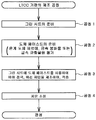
도 2 는 LTCC 기판의 제조 공정의 순서를 나타내는 공정도.
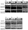
도 3 은 도체 페이스트에 대한 첨가재의 첨가에 의한 은의 확산 억제 효과를 검증한 실험의 결과를 나타내는 설명도.
도 4 는 LTCC 기판의 SEM 화상과, 은의 농도 분포를 나타내는 화상을 나타내는 설명도.
11 : 세라믹 절연층
12 : 비아 전극
13 : 내층 전극
14 : 외부 전극
Claims (7)
- 유리를 함유하는 세라믹 기판의 제조 방법에 있어서,
미소성의 은계 도체 재료를 미소성의 세라믹층에 배치하여 소성하는 소성 공정을 구비하고,
상기 미소성의 은계 도체 재료는, 금속 붕화물을 함유하는 것을 특징으로 하는, 제조 방법. - 제 1 항에 있어서,
상기 금속 붕화물은, 육붕화란탄, 육붕화규소, 이붕화티탄, 이붕화탄탈 중 적어도 하나를 함유하는, 제조 방법. - 제 1 항 또는 제 2 항에 있어서,
상기 미소성의 은계 도체 재료는 상기 금속 붕화물을 함유하고,
상기 미소성의 은계 도체 재료의 무기 성분 중에 있어서의 상기 금속 붕화물의 함유율은 3 체적% 보다 크고, 20 체적% 보다 작은, 제조 방법. - 제 1 항 내지 제 3 항 중 어느 한 항에 있어서,
상기 미소성의 은계 도체 재료는 은 분말을 함유하고,
상기 금속 붕화물은, 상기 은계 도체 재료에 있어서, 상기 은 분말의 표면에 부착되어 있는, 제조 방법. - 세라믹 기판으로서,
제 1 항 내지 제 4 항 중 어느 한 항에 기재된 소성 공정을 거쳐 형성된 세라믹층과, 은계 도체의 배선층을 구비하는, 세라믹 기판. - 세라믹 기판에 있어서 배선층을 형성하고, 미소성의 세라믹층과 동시에 소성되는 미소성의 은계 도체 재료로서,
금속 붕화물을 함유하는 것을 특징으로 하는, 은계 도체 재료. - 유리를 함유하는 세라믹 기판의 제조 방법에 있어서,
미소성의 은계 도체 재료의 입자를 미소성의 세라믹층에 배치하여 소성하는 소성 공정을 구비하고,
상기 미소성의 은계 도체 재료의 입자는, 금속 붕화물 또는 금속 규화물 중 적어도 하나로 코트되어 있는 것을 특징으로 하는, 제조 방법.
Applications Claiming Priority (3)
| Application Number | Priority Date | Filing Date | Title |
|---|---|---|---|
| JP2015003819 | 2015-01-13 | ||
| JPJP-P-2015-003819 | 2015-01-13 | ||
| PCT/JP2016/000082 WO2016114121A1 (ja) | 2015-01-13 | 2016-01-08 | セラミック基板の製造方法、セラミック基板及び銀系導体材料 |
Publications (2)
| Publication Number | Publication Date |
|---|---|
| KR20170094432A true KR20170094432A (ko) | 2017-08-17 |
| KR102028896B1 KR102028896B1 (ko) | 2019-10-07 |
Family
ID=56405670
Family Applications (4)
| Application Number | Title | Priority Date | Filing Date |
|---|---|---|---|
| KR1020177019496A Active KR101994566B1 (ko) | 2015-01-13 | 2016-01-08 | 세라믹 기판 및 그 제조 방법 |
| KR1020177019497A Active KR102017401B1 (ko) | 2015-01-13 | 2016-01-08 | 회로 기판 및 그 제조 방법 |
| KR1020177019498A Active KR102059318B1 (ko) | 2015-01-13 | 2016-01-08 | 세라믹 기판 |
| KR1020177019495A Active KR102028896B1 (ko) | 2015-01-13 | 2016-01-08 | 세라믹 기판의 제조 방법, 세라믹 기판 및 은계 도체 재료 |
Family Applications Before (3)
| Application Number | Title | Priority Date | Filing Date |
|---|---|---|---|
| KR1020177019496A Active KR101994566B1 (ko) | 2015-01-13 | 2016-01-08 | 세라믹 기판 및 그 제조 방법 |
| KR1020177019497A Active KR102017401B1 (ko) | 2015-01-13 | 2016-01-08 | 회로 기판 및 그 제조 방법 |
| KR1020177019498A Active KR102059318B1 (ko) | 2015-01-13 | 2016-01-08 | 세라믹 기판 |
Country Status (6)
| Country | Link |
|---|---|
| US (5) | US20180035549A1 (ko) |
| EP (4) | EP3247181B1 (ko) |
| JP (4) | JP6309631B2 (ko) |
| KR (4) | KR101994566B1 (ko) |
| CN (4) | CN107113969B (ko) |
| WO (4) | WO2016114119A1 (ko) |
Families Citing this family (9)
| Publication number | Priority date | Publication date | Assignee | Title |
|---|---|---|---|---|
| EP3247181B1 (en) * | 2015-01-13 | 2025-02-19 | Niterra Co., Ltd. | Production method of a circuit board |
| CN110255912A (zh) * | 2019-07-03 | 2019-09-20 | 东北大学秦皇岛分校 | 一种微晶玻璃工艺品的制作方法 |
| CN111312427B (zh) * | 2020-04-17 | 2021-08-31 | 洛阳理工学院 | 一种用于低温共烧低介电常数介质陶瓷的多层布线用银浆 |
| CN112225547B (zh) * | 2020-10-19 | 2022-04-19 | 上海晶材新材料科技有限公司 | Ltcc材料、基板及制备方法 |
| CN112235959A (zh) * | 2020-10-28 | 2021-01-15 | 上海读家电子科技有限公司 | 可加强铂钯银导体抗银迁移能力的陶瓷电路板制造方法 |
| CN112216655A (zh) * | 2020-11-03 | 2021-01-12 | 中国电子科技集团公司第四十三研究所 | 一种LTCC基SiP封装外壳及其制备方法 |
| US20220367363A1 (en) * | 2021-05-17 | 2022-11-17 | Onano Industrial Corp. | Ltcc electronic device unit structure |
| CN113690033A (zh) * | 2021-07-23 | 2021-11-23 | 东莞市优琥电子科技有限公司 | 变压器和电源适配器 |
| US20230307314A1 (en) * | 2022-03-24 | 2023-09-28 | Texas Instruments Incorporated | Direct bond copper substrate with metal filled ceramic substrate indentations |
Citations (7)
| Publication number | Priority date | Publication date | Assignee | Title |
|---|---|---|---|---|
| JPH03233831A (ja) * | 1990-02-07 | 1991-10-17 | Dai Ichi Kogyo Seiyaku Co Ltd | 6ホウ化ランタン含有ペースト |
| JPH06252524A (ja) | 1993-02-26 | 1994-09-09 | Asahi Glass Co Ltd | 導体付きセラミックス基板の製造方法 |
| JPH09246722A (ja) * | 1996-03-08 | 1997-09-19 | Sumitomo Metal Ind Ltd | ガラスセラミックス多層配線基板とその製造方法 |
| JP2001278657A (ja) * | 2000-01-24 | 2001-10-10 | Ngk Spark Plug Co Ltd | 低温焼成磁器組成物及びその製造方法並びにその低温焼成磁器組成物を用いた低温焼成配線基板 |
| JP2007059390A (ja) * | 2005-07-28 | 2007-03-08 | E I Du Pont De Nemours & Co | 基板上のltcc感光性テープの適用例で使用される導体組成物 |
| JP2007234537A (ja) | 2006-03-03 | 2007-09-13 | Asahi Glass Co Ltd | 導体ペーストおよびセラミック多層基板製造方法 |
| WO2014026910A1 (en) * | 2012-08-14 | 2014-02-20 | Henkel Ag & Co. Kgaa | Curable compositions comprising composite particles |
Family Cites Families (48)
| Publication number | Priority date | Publication date | Assignee | Title |
|---|---|---|---|---|
| JPS6029240B2 (ja) * | 1977-12-02 | 1985-07-09 | 富士通株式会社 | セラミック回路基板の製法 |
| JPS5491790A (en) * | 1977-12-29 | 1979-07-20 | Junkosha Co Ltd | Flat cable |
| US4279654A (en) * | 1979-05-14 | 1981-07-21 | The Foundation: The Research Institute For Special Inorganic Materials | Process for production of crystallized glass and process for producing composite article using said crystallized glass |
| JPS61168564A (ja) * | 1985-01-18 | 1986-07-30 | 株式会社日立製作所 | セラミツク絶縁基板 |
| US4639391A (en) * | 1985-03-14 | 1987-01-27 | Cts Corporation | Thick film resistive paint and resistors made therefrom |
| DE3621667A1 (de) * | 1985-06-29 | 1987-01-08 | Toshiba Kawasaki Kk | Mit einer mehrzahl von dickfilmen beschichtetes substrat, verfahren zu seiner herstellung und dieses enthaltende vorrichtung |
| US4777014A (en) * | 1986-03-07 | 1988-10-11 | Lanxide Technology Company, Lp | Process for preparing self-supporting bodies and products made thereby |
| JPH0619926B2 (ja) | 1987-11-11 | 1994-03-16 | 株式会社日立製作所 | 回路基板とその製法 |
| DE3935471A1 (de) * | 1989-10-25 | 1991-05-02 | Hoechst Ag | Keramische stoffzusammensetzung und ihre verwendung |
| JPH0719964B2 (ja) * | 1990-08-08 | 1995-03-06 | 日本電気株式会社 | 銀系配線セラミック基板 |
| JPH04314394A (ja) * | 1991-04-12 | 1992-11-05 | Fujitsu Ltd | ガラスセラミック回路基板とその製造方法 |
| JPH0793228B2 (ja) * | 1991-04-24 | 1995-10-09 | 太陽誘電株式会社 | 希土類入り銀導電ペーストおよびこれを用いた電子部品 |
| JP2985503B2 (ja) | 1992-04-22 | 1999-12-06 | 株式会社村田製作所 | 導電ペースト組成物 |
| JPH0595071U (ja) * | 1992-05-28 | 1993-12-24 | 京セラ株式会社 | 厚膜回路基板 |
| EP0575813B1 (en) * | 1992-06-08 | 1996-12-27 | NEC Corporation | Multilayer glass ceramic substrate and process for producing the same |
| JP3448747B2 (ja) * | 1992-08-25 | 2003-09-22 | 松下電器産業株式会社 | 多層セラミック基板の製造方法 |
| DE4345586B4 (de) * | 1992-12-22 | 2009-04-23 | Denso Corp., Kariya-shi | Verfahren zum Erzeugen von Vielfach-Dickschichtsubstraten |
| JPH06204511A (ja) * | 1993-01-07 | 1994-07-22 | Dai Ichi Kogyo Seiyaku Co Ltd | 半導体基板用電極ペースト |
| JPH07135394A (ja) * | 1993-11-09 | 1995-05-23 | Ngk Spark Plug Co Ltd | 厚膜コンデンサ付きセラミック配線基板及びその製造方法 |
| US5474619A (en) * | 1994-05-04 | 1995-12-12 | The United States Of America As Represented By The Secretary Of Commerce | Thin film high temperature silicide thermocouples |
| JPH08259331A (ja) * | 1995-03-22 | 1996-10-08 | Agency Of Ind Science & Technol | 可塑成形用窒化ケイ素−水系組成物の調製法 |
| JPH08298382A (ja) * | 1995-04-26 | 1996-11-12 | Tdk Corp | セラミックス多層基板 |
| JP3927250B2 (ja) * | 1995-08-16 | 2007-06-06 | イー・アイ・デュポン・ドウ・ヌムール・アンド・カンパニー | 窒化アルミニウム基板用厚膜導体ペースト組成物 |
| US5857253A (en) * | 1996-03-20 | 1999-01-12 | Ppg Industries, Inc. | System and methods for forming bushing plates |
| JP4099837B2 (ja) * | 1997-08-27 | 2008-06-11 | 株式会社村田製作所 | 低温焼成セラミック多層基板の製造方法 |
| JPH11339560A (ja) * | 1998-05-29 | 1999-12-10 | Murata Mfg Co Ltd | 銀ペースト |
| CA2478142C (en) * | 2001-03-09 | 2009-09-15 | Datec Coating Corporation | Sol-gel derived resistive and conductive coating |
| JP3636123B2 (ja) * | 2001-09-20 | 2005-04-06 | 株式会社村田製作所 | 積層セラミック電子部品の製造方法、および積層セラミック電子部品 |
| ATE334949T1 (de) * | 2001-10-09 | 2006-08-15 | Du Pont | Dickfilm-leiterzusammensetzungen zur verwendung auf alumniumnitridsubstraten |
| JP2003268567A (ja) * | 2002-03-19 | 2003-09-25 | Hitachi Cable Ltd | 導電材被覆耐食性金属材料 |
| JP3988533B2 (ja) * | 2002-05-23 | 2007-10-10 | 株式会社村田製作所 | ガラスセラミック組成物、ガラスセラミック、およびセラミック多層基板 |
| US7323805B2 (en) * | 2004-01-28 | 2008-01-29 | Kabushiki Kaisha Toshiba | Piezoelectric thin film device and method for manufacturing the same |
| US7218506B2 (en) * | 2004-03-31 | 2007-05-15 | Tdk Corporation | Electrolytic capacitor and method of manufacturing the same |
| JP2006073280A (ja) * | 2004-08-31 | 2006-03-16 | Ngk Spark Plug Co Ltd | メタライズ組成物及びセラミック配線基板 |
| JP4548050B2 (ja) * | 2004-09-03 | 2010-09-22 | 株式会社村田製作所 | セラミック多層基板 |
| JP2006253600A (ja) * | 2005-03-14 | 2006-09-21 | Ngk Spark Plug Co Ltd | 配線基板の製造方法 |
| KR100657321B1 (ko) * | 2005-06-30 | 2006-12-14 | 삼성전자주식회사 | 인쇄데이터 관리방법 및 장치 |
| TW200710882A (en) * | 2005-07-28 | 2007-03-16 | Du Pont | Conductor composition for use in LTCC photosensitive tape on substrate applications |
| JP4797534B2 (ja) | 2005-09-16 | 2011-10-19 | Tdk株式会社 | 多層セラミックス基板 |
| US7666328B2 (en) * | 2005-11-22 | 2010-02-23 | E. I. Du Pont De Nemours And Company | Thick film conductor composition(s) and processing technology thereof for use in multilayer electronic circuits and devices |
| JP4967388B2 (ja) * | 2006-03-15 | 2012-07-04 | パナソニック株式会社 | セラミック積層デバイスの製造方法およびセラミック積層デバイス |
| KR100956219B1 (ko) * | 2008-02-25 | 2010-05-04 | 삼성전기주식회사 | 확산 방지층을 갖는 저온동시소성 세라믹 기판 및 그 제조방법 |
| JPWO2011102040A1 (ja) * | 2010-02-19 | 2013-06-17 | 旭硝子株式会社 | 素子搭載用基板およびその製造方法 |
| JP5488282B2 (ja) | 2010-07-13 | 2014-05-14 | 昭栄化学工業株式会社 | 導電性ペースト |
| JP5949770B2 (ja) * | 2011-08-09 | 2016-07-13 | 旭硝子株式会社 | ガラスセラミックス体、発光素子搭載用基板、および発光装置 |
| JP2013153051A (ja) * | 2012-01-25 | 2013-08-08 | Tokuyama Corp | メタライズドセラミックスビア基板及びその製造方法 |
| JP2014179473A (ja) | 2013-03-15 | 2014-09-25 | Ngk Spark Plug Co Ltd | セラミック基板の製造方法および導体材料 |
| EP3247181B1 (en) * | 2015-01-13 | 2025-02-19 | Niterra Co., Ltd. | Production method of a circuit board |
-
2016
- 2016-01-08 EP EP16737189.7A patent/EP3247181B1/en active Active
- 2016-01-08 US US15/543,253 patent/US20180035549A1/en not_active Abandoned
- 2016-01-08 JP JP2016541726A patent/JP6309631B2/ja active Active
- 2016-01-08 US US15/543,290 patent/US20180014408A1/en not_active Abandoned
- 2016-01-08 US US15/543,264 patent/US10375837B2/en active Active
- 2016-01-08 WO PCT/JP2016/000080 patent/WO2016114119A1/ja not_active Ceased
- 2016-01-08 CN CN201680005732.7A patent/CN107113969B/zh active Active
- 2016-01-08 EP EP16737190.5A patent/EP3247184B1/en active Active
- 2016-01-08 KR KR1020177019496A patent/KR101994566B1/ko active Active
- 2016-01-08 KR KR1020177019497A patent/KR102017401B1/ko active Active
- 2016-01-08 US US15/542,871 patent/US10524365B2/en active Active
- 2016-01-08 KR KR1020177019498A patent/KR102059318B1/ko active Active
- 2016-01-08 CN CN201680005796.7A patent/CN107113976B/zh active Active
- 2016-01-08 CN CN201680005805.2A patent/CN107113986B/zh active Active
- 2016-01-08 KR KR1020177019495A patent/KR102028896B1/ko active Active
- 2016-01-08 EP EP16737192.1A patent/EP3247182A4/en active Pending
- 2016-01-08 WO PCT/JP2016/000079 patent/WO2016114118A1/ja not_active Ceased
- 2016-01-08 WO PCT/JP2016/000081 patent/WO2016114120A1/ja not_active Ceased
- 2016-01-08 JP JP2016542286A patent/JP6309632B2/ja active Active
- 2016-01-08 JP JP2016541735A patent/JP6553048B2/ja active Active
- 2016-01-08 CN CN201680005790.XA patent/CN107211535B/zh active Active
- 2016-01-08 JP JP2016541738A patent/JP6261746B2/ja active Active
- 2016-01-08 WO PCT/JP2016/000082 patent/WO2016114121A1/ja not_active Ceased
- 2016-01-08 EP EP16737191.3A patent/EP3247180B1/en active Active
-
2018
- 2018-07-10 US US16/031,828 patent/US10785879B2/en active Active
Patent Citations (7)
| Publication number | Priority date | Publication date | Assignee | Title |
|---|---|---|---|---|
| JPH03233831A (ja) * | 1990-02-07 | 1991-10-17 | Dai Ichi Kogyo Seiyaku Co Ltd | 6ホウ化ランタン含有ペースト |
| JPH06252524A (ja) | 1993-02-26 | 1994-09-09 | Asahi Glass Co Ltd | 導体付きセラミックス基板の製造方法 |
| JPH09246722A (ja) * | 1996-03-08 | 1997-09-19 | Sumitomo Metal Ind Ltd | ガラスセラミックス多層配線基板とその製造方法 |
| JP2001278657A (ja) * | 2000-01-24 | 2001-10-10 | Ngk Spark Plug Co Ltd | 低温焼成磁器組成物及びその製造方法並びにその低温焼成磁器組成物を用いた低温焼成配線基板 |
| JP2007059390A (ja) * | 2005-07-28 | 2007-03-08 | E I Du Pont De Nemours & Co | 基板上のltcc感光性テープの適用例で使用される導体組成物 |
| JP2007234537A (ja) | 2006-03-03 | 2007-09-13 | Asahi Glass Co Ltd | 導体ペーストおよびセラミック多層基板製造方法 |
| WO2014026910A1 (en) * | 2012-08-14 | 2014-02-20 | Henkel Ag & Co. Kgaa | Curable compositions comprising composite particles |
Also Published As
Similar Documents
| Publication | Publication Date | Title |
|---|---|---|
| KR20170094432A (ko) | 세라믹 기판의 제조 방법, 세라믹 기판 및 은계 도체 재료 | |
| KR20110083624A (ko) | 세라믹 적층 부품과 그 제조 방법 | |
| JPH0563110B2 (ko) | ||
| JP6693836B2 (ja) | セラミック配線基板及びセラミック配線基板の製造方法 | |
| JP2008277628A (ja) | セラミック基板の製造方法、セラミック基板、および電子装置 | |
| JP4820149B2 (ja) | 導電性ペーストの製造方法および配線基板の製造方法 | |
| JP2022076097A (ja) | セラミック配線基板およびセラミック配線基板の製造方法 |
Legal Events
| Date | Code | Title | Description |
|---|---|---|---|
| A201 | Request for examination | ||
| PA0105 | International application |
Patent event date: 20170713 Patent event code: PA01051R01D Comment text: International Patent Application |
|
| PA0201 | Request for examination | ||
| PG1501 | Laying open of application | ||
| E902 | Notification of reason for refusal | ||
| PE0902 | Notice of grounds for rejection |
Comment text: Notification of reason for refusal Patent event date: 20181206 Patent event code: PE09021S01D |
|
| E902 | Notification of reason for refusal | ||
| PE0902 | Notice of grounds for rejection |
Comment text: Notification of reason for refusal Patent event date: 20190618 Patent event code: PE09021S01D |
|
| E701 | Decision to grant or registration of patent right | ||
| PE0701 | Decision of registration |
Patent event code: PE07011S01D Comment text: Decision to Grant Registration Patent event date: 20190821 |
|
| GRNT | Written decision to grant | ||
| PR0701 | Registration of establishment |
Comment text: Registration of Establishment Patent event date: 20190930 Patent event code: PR07011E01D |
|
| PR1002 | Payment of registration fee |
Payment date: 20190930 End annual number: 3 Start annual number: 1 |
|
| PG1601 | Publication of registration | ||
| PR1001 | Payment of annual fee |
Payment date: 20220902 Start annual number: 4 End annual number: 4 |
|
| PR1001 | Payment of annual fee |
Payment date: 20230829 Start annual number: 5 End annual number: 5 |
|
| PR1001 | Payment of annual fee |
Payment date: 20240829 Start annual number: 6 End annual number: 6 |