KR20170136634A - 전자 부품을 테스트하는 방법 - Google Patents
전자 부품을 테스트하는 방법 Download PDFInfo
- Publication number
- KR20170136634A KR20170136634A KR1020177032972A KR20177032972A KR20170136634A KR 20170136634 A KR20170136634 A KR 20170136634A KR 1020177032972 A KR1020177032972 A KR 1020177032972A KR 20177032972 A KR20177032972 A KR 20177032972A KR 20170136634 A KR20170136634 A KR 20170136634A
- Authority
- KR
- South Korea
- Prior art keywords
- electronic component
- production line
- ray
- circuit board
- areas
- Prior art date
- Legal status (The legal status is an assumption and is not a legal conclusion. Google has not performed a legal analysis and makes no representation as to the accuracy of the status listed.)
- Granted
Links
Images
Classifications
-
- G—PHYSICS
- G01—MEASURING; TESTING
- G01N—INVESTIGATING OR ANALYSING MATERIALS BY DETERMINING THEIR CHEMICAL OR PHYSICAL PROPERTIES
- G01N23/00—Investigating or analysing materials by the use of wave or particle radiation, e.g. X-rays or neutrons, not covered by groups G01N3/00 – G01N17/00, G01N21/00 or G01N22/00
- G01N23/02—Investigating or analysing materials by the use of wave or particle radiation, e.g. X-rays or neutrons, not covered by groups G01N3/00 – G01N17/00, G01N21/00 or G01N22/00 by transmitting the radiation through the material
- G01N23/06—Investigating or analysing materials by the use of wave or particle radiation, e.g. X-rays or neutrons, not covered by groups G01N3/00 – G01N17/00, G01N21/00 or G01N22/00 by transmitting the radiation through the material and measuring the absorption
- G01N23/083—Investigating or analysing materials by the use of wave or particle radiation, e.g. X-rays or neutrons, not covered by groups G01N3/00 – G01N17/00, G01N21/00 or G01N22/00 by transmitting the radiation through the material and measuring the absorption the radiation being X-rays
-
- G—PHYSICS
- G01—MEASURING; TESTING
- G01N—INVESTIGATING OR ANALYSING MATERIALS BY DETERMINING THEIR CHEMICAL OR PHYSICAL PROPERTIES
- G01N23/00—Investigating or analysing materials by the use of wave or particle radiation, e.g. X-rays or neutrons, not covered by groups G01N3/00 – G01N17/00, G01N21/00 or G01N22/00
- G01N23/02—Investigating or analysing materials by the use of wave or particle radiation, e.g. X-rays or neutrons, not covered by groups G01N3/00 – G01N17/00, G01N21/00 or G01N22/00 by transmitting the radiation through the material
- G01N23/06—Investigating or analysing materials by the use of wave or particle radiation, e.g. X-rays or neutrons, not covered by groups G01N3/00 – G01N17/00, G01N21/00 or G01N22/00 by transmitting the radiation through the material and measuring the absorption
- G01N23/18—Investigating the presence of flaws defects or foreign matter
-
- G—PHYSICS
- G01—MEASURING; TESTING
- G01N—INVESTIGATING OR ANALYSING MATERIALS BY DETERMINING THEIR CHEMICAL OR PHYSICAL PROPERTIES
- G01N21/00—Investigating or analysing materials by the use of optical means, i.e. using sub-millimetre waves, infrared, visible or ultraviolet light
- G01N21/84—Systems specially adapted for particular applications
- G01N21/88—Investigating the presence of flaws or contamination
- G01N21/8851—Scan or image signal processing specially adapted therefor, e.g. for scan signal adjustment, for detecting different kinds of defects, for compensating for structures, markings, edges
-
- G—PHYSICS
- G01—MEASURING; TESTING
- G01N—INVESTIGATING OR ANALYSING MATERIALS BY DETERMINING THEIR CHEMICAL OR PHYSICAL PROPERTIES
- G01N21/00—Investigating or analysing materials by the use of optical means, i.e. using sub-millimetre waves, infrared, visible or ultraviolet light
- G01N21/84—Systems specially adapted for particular applications
- G01N21/88—Investigating the presence of flaws or contamination
- G01N21/95—Investigating the presence of flaws or contamination characterised by the material or shape of the object to be examined
- G01N21/9501—Semiconductor wafers
-
- G—PHYSICS
- G06—COMPUTING OR CALCULATING; COUNTING
- G06K—GRAPHICAL DATA READING; PRESENTATION OF DATA; RECORD CARRIERS; HANDLING RECORD CARRIERS
- G06K7/00—Methods or arrangements for sensing record carriers, e.g. for reading patterns
- G06K7/10—Methods or arrangements for sensing record carriers, e.g. for reading patterns by electromagnetic radiation, e.g. optical sensing; by corpuscular radiation
- G06K7/14—Methods or arrangements for sensing record carriers, e.g. for reading patterns by electromagnetic radiation, e.g. optical sensing; by corpuscular radiation using light without selection of wavelength, e.g. sensing reflected white light
- G06K7/1404—Methods for optical code recognition
- G06K7/1408—Methods for optical code recognition the method being specifically adapted for the type of code
- G06K7/1413—1D bar codes
-
- G—PHYSICS
- G06—COMPUTING OR CALCULATING; COUNTING
- G06T—IMAGE DATA PROCESSING OR GENERATION, IN GENERAL
- G06T7/00—Image analysis
- G06T7/0002—Inspection of images, e.g. flaw detection
- G06T7/0004—Industrial image inspection
-
- G—PHYSICS
- G06—COMPUTING OR CALCULATING; COUNTING
- G06T—IMAGE DATA PROCESSING OR GENERATION, IN GENERAL
- G06T7/00—Image analysis
- G06T7/0002—Inspection of images, e.g. flaw detection
- G06T7/0004—Industrial image inspection
- G06T7/001—Industrial image inspection using an image reference approach
-
- G—PHYSICS
- G01—MEASURING; TESTING
- G01N—INVESTIGATING OR ANALYSING MATERIALS BY DETERMINING THEIR CHEMICAL OR PHYSICAL PROPERTIES
- G01N21/00—Investigating or analysing materials by the use of optical means, i.e. using sub-millimetre waves, infrared, visible or ultraviolet light
- G01N21/84—Systems specially adapted for particular applications
- G01N21/88—Investigating the presence of flaws or contamination
- G01N21/95—Investigating the presence of flaws or contamination characterised by the material or shape of the object to be examined
- G01N21/956—Inspecting patterns on the surface of objects
- G01N2021/95638—Inspecting patterns on the surface of objects for PCB's
-
- G—PHYSICS
- G01—MEASURING; TESTING
- G01N—INVESTIGATING OR ANALYSING MATERIALS BY DETERMINING THEIR CHEMICAL OR PHYSICAL PROPERTIES
- G01N21/00—Investigating or analysing materials by the use of optical means, i.e. using sub-millimetre waves, infrared, visible or ultraviolet light
- G01N21/84—Systems specially adapted for particular applications
- G01N21/88—Investigating the presence of flaws or contamination
- G01N21/95—Investigating the presence of flaws or contamination characterised by the material or shape of the object to be examined
-
- G—PHYSICS
- G01—MEASURING; TESTING
- G01N—INVESTIGATING OR ANALYSING MATERIALS BY DETERMINING THEIR CHEMICAL OR PHYSICAL PROPERTIES
- G01N2223/00—Investigating materials by wave or particle radiation
- G01N2223/60—Specific applications or type of materials
- G01N2223/611—Specific applications or type of materials patterned objects; electronic devices
- G01N2223/6113—Specific applications or type of materials patterned objects; electronic devices printed circuit board [PCB]
-
- G—PHYSICS
- G01—MEASURING; TESTING
- G01N—INVESTIGATING OR ANALYSING MATERIALS BY DETERMINING THEIR CHEMICAL OR PHYSICAL PROPERTIES
- G01N2223/00—Investigating materials by wave or particle radiation
- G01N2223/60—Specific applications or type of materials
- G01N2223/66—Specific applications or type of materials multiple steps inspection, e.g. coarse/fine
-
- G—PHYSICS
- G06—COMPUTING OR CALCULATING; COUNTING
- G06T—IMAGE DATA PROCESSING OR GENERATION, IN GENERAL
- G06T2207/00—Indexing scheme for image analysis or image enhancement
- G06T2207/10—Image acquisition modality
- G06T2207/10116—X-ray image
-
- G—PHYSICS
- G06—COMPUTING OR CALCULATING; COUNTING
- G06T—IMAGE DATA PROCESSING OR GENERATION, IN GENERAL
- G06T2207/00—Indexing scheme for image analysis or image enhancement
- G06T2207/30—Subject of image; Context of image processing
- G06T2207/30108—Industrial image inspection
- G06T2207/30141—Printed circuit board [PCB]
Landscapes
- Engineering & Computer Science (AREA)
- Physics & Mathematics (AREA)
- General Physics & Mathematics (AREA)
- Health & Medical Sciences (AREA)
- General Health & Medical Sciences (AREA)
- Life Sciences & Earth Sciences (AREA)
- Pathology (AREA)
- Immunology (AREA)
- Biochemistry (AREA)
- Analytical Chemistry (AREA)
- Chemical & Material Sciences (AREA)
- Computer Vision & Pattern Recognition (AREA)
- Theoretical Computer Science (AREA)
- Quality & Reliability (AREA)
- Toxicology (AREA)
- Electromagnetism (AREA)
- Artificial Intelligence (AREA)
- Signal Processing (AREA)
- Analysing Materials By The Use Of Radiation (AREA)
- Investigating Materials By The Use Of Optical Means Adapted For Particular Applications (AREA)
Abstract
Description
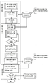
도 1은 본 발명에 따른 방법의 흐름도이다.
Claims (9)
- 전자 부품의 결함을 테스트하는 방법으로서,
- 자동 광학 검사를 통해 생산 라인 내의 전자 부품을 검사하는 단계;
- 자동 광학 검사를 사용하여 검사가 불가능한 영역들의 좌표를 결정하는 단계;
- 상기 영역들의 좌표를 생산 라인으로부터 컴퓨터로 전송하는 단계;
- 비파괴 재료 테스트(non-destructive material testing)을 위해, 전자 부품을 생산 라인으로부터, 상기 생산 라인 외부에 위치한 X-선 장치로 이송하는 단계;
- 상기 영역들의 좌표를 컴퓨터로부터 X-선 장치로 전송하는 단계;
- 상기 자동 광학 검사를 사용하여 검사가 불가능한 영역들에 대해서만, X-선 장치를 사용하여 상기 전자 부품을 검사하는 단계;
- 상기 X-선 장치의 검사 결과를 컴퓨터로 전송하는 단계; 및
- 상기 검사 결과가 결함이 없다고 표시하면, 상기 전자 부품을 생산 라인으로 복귀시키는 단계;를 포함하는 전자 부품 결함 테스트 방법. - 제 1 항에 있어서,
상기 전자 부품은, 상기 전자 부품이 명확하게 식별 가능하게 하는 식별자를 가지고, 상기 식별자는 자동 광학 검사를 이용하여 검사가 불가능한 영역들의 좌표와 함께, 생산 라인으로부터 X-선 장치로 컴퓨터에 전송되며,
상기 식별자는 X-선 장치에서 검출되고, 이러한 데이터들은 컴퓨터로 전송되고, 컴퓨터에서 상기 데이터들은 생산 라인 및 X-선 장치로부터의 식별자와 비교되는, 전자 부품 결함 테스트 방법. - 제 2 항에 있어서,
상기 식별자는, X-선 장치에서 바코드 판독 장치에 의해 검출되는 바코드인, 전자 부품 결함 테스트 방법. - 제 1 항 내지 제 3 항 중 어느 한 항에 있어서,
생산 라인과 X-선 장치 사이의 상기 전자 부품의 이송 및/또는 복귀는 자동적으로 실행되는, 전자 부품 결함 테스트 방법. - 제 1 항 내지 제 4 항 중 어느 한 항에 있어서,
상기 자동 광학 검사를 사용하여 검사가 불가능한 영역들의 좌표는, 예를 들어, 회로 기판의 코너(corner) 또는 수납 트레이의 코너 또는 특징적인 구멍과 같은, 전자 부품의 명확한 특징을 갖는 위치에 대해 결정되는, 전자 부품 결함 테스트 방법. - 제 5 항에 있어서,
상기 전자 부품 또는 수납 트레이의 정렬은 X-선 장치에서 회로 기판의 상기 명확한 특징을 갖는 위치를 기준으로 이루어지는, 전자 부품 결함 테스트 방법. - 제 1 항 내지 제 6 항 중 어느 한 항에 있어서,
X-선 장치에서의 검사에 의해, 확정된 결함의 유형이 얻어지고, 이 정보를 사용하여, 상기 결함의 유형이 회피되도록 생산 라인에서 공정의 제어가 이루어지는, 전자 부품 결함 테스트 방법. - 제 1 항 내지 제 7 항 중 어느 한 항에 있어서,
상기 전자 부품은 인쇄 회로 기판 어셈블리, 에칭된 구조물 및 마이크로 솔더 볼(micro solder ball)을 갖는 웨이퍼, 또는 예를 들어 반도체 또는 LED와 같은 전자 부품인, 전자 부품 결함 테스트 방법. - 제 1 항 내지 제 8 항 중 어느 한 항에 있어서,
상기 X-선 장치에서, 개방형 마이크로포커스 튜브(open microfocus tube), 특히 10 와트보다 큰 목표 출력을 갖는 개방형 마이크로포커스 튜브가 사용되는, 전자 부품 결함 테스트 방법.
Applications Claiming Priority (5)
| Application Number | Priority Date | Filing Date | Title |
|---|---|---|---|
| DE102015004650.0 | 2015-04-15 | ||
| DE102015004650 | 2015-04-15 | ||
| DE102015005641.7 | 2015-05-05 | ||
| DE102015005641.7A DE102015005641A1 (de) | 2015-05-05 | 2015-05-05 | Verfahren zum Prüfen eines elektronischen Bauteils |
| PCT/EP2016/000612 WO2016165828A1 (de) | 2015-04-15 | 2016-04-14 | Verfahren zum prüfen eines elektronischen bauteils |
Publications (2)
| Publication Number | Publication Date |
|---|---|
| KR20170136634A true KR20170136634A (ko) | 2017-12-11 |
| KR102121521B1 KR102121521B1 (ko) | 2020-06-29 |
Family
ID=55808541
Family Applications (1)
| Application Number | Title | Priority Date | Filing Date |
|---|---|---|---|
| KR1020177032972A Active KR102121521B1 (ko) | 2015-04-15 | 2016-04-14 | 전자 부품을 테스트하는 방법 |
Country Status (6)
| Country | Link |
|---|---|
| US (1) | US10571413B2 (ko) |
| JP (1) | JP6535755B2 (ko) |
| KR (1) | KR102121521B1 (ko) |
| CN (1) | CN107592910B (ko) |
| TW (1) | TW201643411A (ko) |
| WO (1) | WO2016165828A1 (ko) |
Cited By (1)
| Publication number | Priority date | Publication date | Assignee | Title |
|---|---|---|---|---|
| KR20220133575A (ko) | 2021-03-25 | 2022-10-05 | 스템코 주식회사 | 광학 검사 장치 |
Families Citing this family (7)
| Publication number | Priority date | Publication date | Assignee | Title |
|---|---|---|---|---|
| GB2574188B (en) * | 2018-04-11 | 2022-03-09 | E M & I Maritime Ltd | Inspection of hazardous area equipment |
| US11188792B2 (en) | 2020-01-07 | 2021-11-30 | International Business Machines Corporation | Defect detection using multiple models |
| US20240155250A1 (en) * | 2021-04-14 | 2024-05-09 | Mintit Co., Ltd. | Method for Testing Mobile Electronic Device in Automated Device, and Mobile Electronic Device Test System |
| CN113252686B (zh) * | 2021-05-13 | 2021-12-17 | 中科长光精拓智能装备(苏州)有限公司 | 一种电子元件邦定方法 |
| US12416589B2 (en) | 2022-06-24 | 2025-09-16 | SanDisk Technologies, Inc. | Systems and methods for non-destructive inspection of semiconductor devices using reflective X-ray microscope tomographic imaging |
| US12651329B2 (en) * | 2023-10-31 | 2026-06-09 | Motorola Solutions, Inc. | System, device and method for detection of counterfeit electronic products |
| WO2025218899A1 (en) * | 2024-04-18 | 2025-10-23 | Fraunhofer-Gesellschaft zur Förderung der angewandten Forschung e. V. | Method for testing devices and inspection system |
Citations (4)
| Publication number | Priority date | Publication date | Assignee | Title |
|---|---|---|---|---|
| JPH0669700A (ja) * | 1992-08-21 | 1994-03-11 | Fujitsu Ltd | プリント板ユニット外観検査システム |
| JPH0635225U (ja) * | 1992-10-20 | 1994-05-10 | 富士通テン株式会社 | 立体交差型生産ライン |
| JP2000275191A (ja) * | 1999-03-25 | 2000-10-06 | Techno Enami:Kk | X線検査方法及びその装置 |
| JP2011018696A (ja) * | 2009-07-07 | 2011-01-27 | Hitachi Ltd | 電子部品組立生産システム |
Family Cites Families (49)
| Publication number | Priority date | Publication date | Assignee | Title |
|---|---|---|---|---|
| DE2440146C3 (de) * | 1974-08-21 | 1981-05-14 | Siemens AG, 1000 Berlin und 8000 München | Röntgenuntersuchungsgerät mit einer Schichtaufnahmeeinrichtung |
| US4365895A (en) * | 1980-12-03 | 1982-12-28 | Probex, Inc. | Method, apparatus and film strip of particular design for rapid test of a film processor |
| EP0512620A3 (en) * | 1991-05-07 | 1995-07-05 | Koninklijke Philips Electronics N.V. | X-ray analysis apparatus |
| IL101063A (en) * | 1992-02-25 | 1995-03-30 | Orbotech Ltd | Verification and repair station for pcbs |
| JPH05329753A (ja) * | 1992-05-26 | 1993-12-14 | Hitachi Ltd | 自動生産ライン設備制御方式 |
| JPH07306165A (ja) * | 1994-05-12 | 1995-11-21 | Toshiba Corp | X線検査装置およびx線検査補修装置 |
| US5963662A (en) * | 1996-08-07 | 1999-10-05 | Georgia Tech Research Corporation | Inspection system and method for bond detection and validation of surface mount devices |
| JP3883153B2 (ja) * | 1998-04-10 | 2007-02-21 | 松下電器産業株式会社 | X線基板検査装置 |
| JPH11330178A (ja) * | 1998-05-13 | 1999-11-30 | Advantest Corp | 表面検査装置および方法 |
| JP2991204B2 (ja) * | 1998-12-25 | 1999-12-20 | 株式会社日立製作所 | 検査装置 |
| CA2296143A1 (fr) * | 2000-01-18 | 2001-07-18 | 9071 9410 Quebec Inc. | Systeme d'inspection optique |
| SE0000314D0 (sv) * | 2000-01-31 | 2000-01-31 | Astrazeneca Ab | Apparatus and method for analysing |
| US6725115B2 (en) * | 2000-05-08 | 2004-04-20 | Teradyne, Inc. | Dynamic testing of electronic assemblies |
| WO2002003045A2 (en) * | 2000-06-30 | 2002-01-10 | Testship Automatic Test Soluti | Probe, systems and methods for integrated circuit board testing |
| US20040004482A1 (en) * | 2002-04-18 | 2004-01-08 | Photon Dynamics, Inc. | Industrial inspection using combination of functional testing and structural inspection |
| US7042564B2 (en) * | 2002-08-08 | 2006-05-09 | Applied Materials, Israel, Ltd. | Wafer inspection methods and an optical inspection tool |
| US6895565B2 (en) * | 2002-10-08 | 2005-05-17 | Agilent Technologies, Inc. | Methods for predicting board test coverage |
| US6903360B2 (en) * | 2002-10-16 | 2005-06-07 | Agilent Technologies, Inc. | Method for detecting missing components at electrical board test using optoelectronic fixture-mounted sensors |
| EP2365324A3 (en) * | 2003-08-06 | 2011-11-16 | Bridger Technologies, Inc. | Bridged element for detection of a target substance |
| US7015492B2 (en) * | 2003-08-15 | 2006-03-21 | Asm International N.V. | Method and apparatus for mapping of wafers located inside a closed wafer cassette |
| AU2003269535A1 (en) * | 2003-10-14 | 2005-04-27 | Mirtec Co., Ltd. | Printed circuit board inspection system combining x-ray inspection and visual inspection |
| US7492449B2 (en) * | 2004-04-12 | 2009-02-17 | Georgia Tech Research Corporation | Inspection systems and methods |
| US7366321B2 (en) * | 2004-06-18 | 2008-04-29 | Agilent Technologies, Inc. | System and method for performing automated optical inspection of objects |
| JP2006189281A (ja) * | 2005-01-05 | 2006-07-20 | Hitachi High-Technologies Corp | 表面検査装置及び表面検査方法 |
| WO2007005636A2 (en) * | 2005-06-30 | 2007-01-11 | Controlled Semiconductor, Inc. | Semiconductor failure analysis tool |
| CN100514348C (zh) | 2005-08-05 | 2009-07-15 | 深圳普诺玛商业安全设备有限公司 | 一种屠宰生产线识别及控制系统及其识别方法 |
| JP4746991B2 (ja) * | 2006-01-17 | 2011-08-10 | 株式会社サキコーポレーション | 被検査体の検査装置 |
| CN101370711A (zh) * | 2006-01-17 | 2009-02-18 | 诺瓦提斯公司 | 检测封装中是否存在眼用透镜的方法和装置 |
| KR20070081282A (ko) * | 2006-02-10 | 2007-08-16 | 삼성전자주식회사 | 반도체 디바이스 검사 장치 |
| GB2438439A (en) * | 2006-05-27 | 2007-11-28 | X Tek Systems Ltd | An automatic x-ray inspection system |
| US20080083816A1 (en) * | 2006-10-04 | 2008-04-10 | Leinbach Glen E | Statistical process control of solder paste stenciling using a replicated solder paste feature distributed across a printed circuit board |
| TWI310983B (en) * | 2006-10-24 | 2009-06-11 | Au Optronics Corp | Integrated circuit structure, display module, and inspection method thereof |
| US7991214B1 (en) * | 2007-04-18 | 2011-08-02 | Avaya Inc. | Method to enhance X-ray and optical images and locate nano-scale cracks in electric devices and components |
| WO2009093341A1 (ja) * | 2008-01-21 | 2009-07-30 | Toppan Printing Co., Ltd. | 検査方法及び検査装置 |
| GB0905006D0 (en) * | 2009-03-24 | 2009-05-06 | Rawlinson Paul | Testing and mounting IC's on PCB's |
| JP4883131B2 (ja) * | 2009-04-17 | 2012-02-22 | パナソニック株式会社 | 電子部品実装方法 |
| CN101759139B (zh) | 2009-12-10 | 2013-06-12 | 江苏大学 | Mems微器件的表面改性处理方法及装置 |
| GB201019537D0 (en) * | 2010-11-18 | 2010-12-29 | 20X20 Vision Ltd | PCB reflow inspection angled measurement |
| JP2012184936A (ja) * | 2011-03-03 | 2012-09-27 | Shimadzu Corp | X線検査装置 |
| CN102313744A (zh) * | 2011-03-29 | 2012-01-11 | 上海华碧检测技术有限公司 | 一种pcb板失效分析方法 |
| US20140119511A1 (en) * | 2011-06-15 | 2014-05-01 | Michael Ward | Methods of Identifying Original and Counterfeit Articles using Micro X-Ray Diffraction Mapping |
| US20140010952A1 (en) * | 2012-01-02 | 2014-01-09 | Noam ROSENSTEIN | Pcb repair of defective interconnects by deposition of conductive ink |
| JP5912553B2 (ja) * | 2012-01-12 | 2016-04-27 | ヤマハ発動機株式会社 | プリント基板の複合検査装置 |
| JP5776605B2 (ja) * | 2012-03-30 | 2015-09-09 | オムロン株式会社 | 基板検査結果の分析作業支援用の情報表示システムおよび分析作業の支援方法 |
| CN102682166B (zh) * | 2012-05-09 | 2014-01-15 | 上海望友信息科技有限公司 | Smt设备快速制程系统及方法 |
| US9612284B2 (en) * | 2012-08-27 | 2017-04-04 | Futurewei Technologies, Inc. | System and method for hybrid board-level diagnostics |
| JP5720028B1 (ja) * | 2013-10-03 | 2015-05-20 | 株式会社 システムスクエア | 包装体の検査装置 |
| KR101890281B1 (ko) * | 2016-08-18 | 2018-08-22 | 한국과학기술원 | 볼 그리드 어레이형 반도체 칩 패키지의 검사 방법 |
| US10586318B2 (en) * | 2016-10-07 | 2020-03-10 | Raytheon Company | Automated model-based inspection system for screening electronic components |
-
2016
- 2016-04-14 KR KR1020177032972A patent/KR102121521B1/ko active Active
- 2016-04-14 US US15/564,311 patent/US10571413B2/en active Active
- 2016-04-14 CN CN201680021844.1A patent/CN107592910B/zh active Active
- 2016-04-14 JP JP2017550757A patent/JP6535755B2/ja active Active
- 2016-04-14 WO PCT/EP2016/000612 patent/WO2016165828A1/de not_active Ceased
- 2016-04-15 TW TW105111918A patent/TW201643411A/zh unknown
Patent Citations (4)
| Publication number | Priority date | Publication date | Assignee | Title |
|---|---|---|---|---|
| JPH0669700A (ja) * | 1992-08-21 | 1994-03-11 | Fujitsu Ltd | プリント板ユニット外観検査システム |
| JPH0635225U (ja) * | 1992-10-20 | 1994-05-10 | 富士通テン株式会社 | 立体交差型生産ライン |
| JP2000275191A (ja) * | 1999-03-25 | 2000-10-06 | Techno Enami:Kk | X線検査方法及びその装置 |
| JP2011018696A (ja) * | 2009-07-07 | 2011-01-27 | Hitachi Ltd | 電子部品組立生産システム |
Cited By (1)
| Publication number | Priority date | Publication date | Assignee | Title |
|---|---|---|---|---|
| KR20220133575A (ko) | 2021-03-25 | 2022-10-05 | 스템코 주식회사 | 광학 검사 장치 |
Also Published As
| Publication number | Publication date |
|---|---|
| HK1244057A1 (zh) | 2018-07-27 |
| CN107592910B (zh) | 2021-08-13 |
| US10571413B2 (en) | 2020-02-25 |
| US20180136145A1 (en) | 2018-05-17 |
| JP6535755B2 (ja) | 2019-06-26 |
| WO2016165828A1 (de) | 2016-10-20 |
| CN107592910A (zh) | 2018-01-16 |
| JP2018514760A (ja) | 2018-06-07 |
| KR102121521B1 (ko) | 2020-06-29 |
| TW201643411A (zh) | 2016-12-16 |
Similar Documents
| Publication | Publication Date | Title |
|---|---|---|
| KR102121521B1 (ko) | 전자 부품을 테스트하는 방법 | |
| US8976348B2 (en) | Wafer inspection system | |
| CA2259659C (en) | Automatic semiconductor wafer sorter/prober with extended optical inspection | |
| KR100863140B1 (ko) | 반도체 웨이퍼의 이물 검사 및 리페어 시스템과 그 방법 | |
| CN1818542B (zh) | 已安装的电子部件的检查方法以及装置 | |
| US20120327215A1 (en) | High speed optical sensor inspection system | |
| CN102023161B (zh) | 获取缺陷图像的方法 | |
| KR101372995B1 (ko) | 결함 검사방법 | |
| JP6092602B2 (ja) | 欠陥検査装置及び欠陥検査方法 | |
| US9767547B2 (en) | Inspection method and inspection apparatus | |
| CN114450582B (zh) | 外观检查装置及不良检查方法 | |
| CN112204384B (zh) | 切割芯片检查装置 | |
| KR101661687B1 (ko) | X-ray 기반의 PCB 불량 판정 방법 및 장치 | |
| KR20150084623A (ko) | 회로기판의 블라인드 비아홀 내의 결함의 검사장치, 검사시스템 및 그 검사방법 | |
| KR101745883B1 (ko) | 인쇄회로기판의 광학 검사 장치 및 방법 | |
| JP6387620B2 (ja) | 品質管理システム | |
| US20080205746A1 (en) | Method of inspecting an identification mark, method of inspecting a wafer using the same, and apparatus for performing the method | |
| CN114113142A (zh) | 半导体器件的缺陷检测方法、装置及电子设备 | |
| KR20210021171A (ko) | 제품 검사 장치 및 방법과, 이를 이용한 반도체 제조 시스템 및 제조 방법 | |
| KR102764199B1 (ko) | 웨이퍼 외관 검사 장치 및 방법 | |
| KR101124566B1 (ko) | 웨이퍼 검사장치 | |
| HK1244057B (en) | Method for checking an electronic component | |
| DE102015005641A1 (de) | Verfahren zum Prüfen eines elektronischen Bauteils | |
| Brunelle et al. | Line scan vision system | |
| KR20060039369A (ko) | 웨이퍼 로트 아이디 검사방법 |
Legal Events
| Date | Code | Title | Description |
|---|---|---|---|
| PA0105 | International application |
Patent event date: 20171114 Patent event code: PA01051R01D Comment text: International Patent Application |
|
| PG1501 | Laying open of application | ||
| A201 | Request for examination | ||
| PA0201 | Request for examination |
Patent event code: PA02012R01D Patent event date: 20180312 Comment text: Request for Examination of Application |
|
| E902 | Notification of reason for refusal | ||
| PE0902 | Notice of grounds for rejection |
Comment text: Notification of reason for refusal Patent event date: 20190710 Patent event code: PE09021S01D |
|
| E701 | Decision to grant or registration of patent right | ||
| PE0701 | Decision of registration |
Patent event code: PE07011S01D Comment text: Decision to Grant Registration Patent event date: 20200522 |
|
| GRNT | Written decision to grant | ||
| PR0701 | Registration of establishment |
Comment text: Registration of Establishment Patent event date: 20200604 Patent event code: PR07011E01D |
|
| PR1002 | Payment of registration fee |
Payment date: 20200605 End annual number: 3 Start annual number: 1 |
|
| PG1601 | Publication of registration | ||
| PR1001 | Payment of annual fee |
Payment date: 20230525 Start annual number: 4 End annual number: 4 |
|
| PR1001 | Payment of annual fee |
Payment date: 20250527 Start annual number: 6 End annual number: 6 |