KR20200068785A - 연마 모니터링 시스템 및 연마 모니터링 방법 - Google Patents
연마 모니터링 시스템 및 연마 모니터링 방법 Download PDFInfo
- Publication number
- KR20200068785A KR20200068785A KR1020180155045A KR20180155045A KR20200068785A KR 20200068785 A KR20200068785 A KR 20200068785A KR 1020180155045 A KR1020180155045 A KR 1020180155045A KR 20180155045 A KR20180155045 A KR 20180155045A KR 20200068785 A KR20200068785 A KR 20200068785A
- Authority
- KR
- South Korea
- Prior art keywords
- substrate
- thickness
- inorganic film
- polishing
- spectrum
- Prior art date
- Legal status (The legal status is an assumption and is not a legal conclusion. Google has not performed a legal analysis and makes no representation as to the accuracy of the status listed.)
- Ceased
Links
Images


Classifications
-
- B—PERFORMING OPERATIONS; TRANSPORTING
- B24—GRINDING; POLISHING
- B24B—MACHINES, DEVICES, OR PROCESSES FOR GRINDING OR POLISHING; DRESSING OR CONDITIONING OF ABRADING SURFACES; FEEDING OF GRINDING, POLISHING, OR LAPPING AGENTS
- B24B37/00—Lapping machines or devices; Accessories
- B24B37/005—Control means for lapping machines or devices
-
- H01L21/67242—
-
- H—ELECTRICITY
- H10—SEMICONDUCTOR DEVICES; ELECTRIC SOLID-STATE DEVICES NOT OTHERWISE PROVIDED FOR
- H10P—GENERIC PROCESSES OR APPARATUS FOR THE MANUFACTURE OR TREATMENT OF DEVICES COVERED BY CLASS H10
- H10P72/00—Handling or holding of wafers, substrates or devices during manufacture or treatment thereof
- H10P72/06—Apparatus for monitoring, sorting, marking, testing or measuring
-
- B—PERFORMING OPERATIONS; TRANSPORTING
- B24—GRINDING; POLISHING
- B24B—MACHINES, DEVICES, OR PROCESSES FOR GRINDING OR POLISHING; DRESSING OR CONDITIONING OF ABRADING SURFACES; FEEDING OF GRINDING, POLISHING, OR LAPPING AGENTS
- B24B1/00—Processes of grinding or polishing; Use of auxiliary equipment in connection with such processes
-
- B—PERFORMING OPERATIONS; TRANSPORTING
- B24—GRINDING; POLISHING
- B24B—MACHINES, DEVICES, OR PROCESSES FOR GRINDING OR POLISHING; DRESSING OR CONDITIONING OF ABRADING SURFACES; FEEDING OF GRINDING, POLISHING, OR LAPPING AGENTS
- B24B29/00—Machines or devices for polishing surfaces on work by means of tools made of soft or flexible material with or without the application of solid or liquid polishing agents
- B24B29/02—Machines or devices for polishing surfaces on work by means of tools made of soft or flexible material with or without the application of solid or liquid polishing agents designed for particular workpieces
-
- B—PERFORMING OPERATIONS; TRANSPORTING
- B24—GRINDING; POLISHING
- B24B—MACHINES, DEVICES, OR PROCESSES FOR GRINDING OR POLISHING; DRESSING OR CONDITIONING OF ABRADING SURFACES; FEEDING OF GRINDING, POLISHING, OR LAPPING AGENTS
- B24B37/00—Lapping machines or devices; Accessories
- B24B37/005—Control means for lapping machines or devices
- B24B37/013—Devices or means for detecting lapping completion
-
- B—PERFORMING OPERATIONS; TRANSPORTING
- B24—GRINDING; POLISHING
- B24B—MACHINES, DEVICES, OR PROCESSES FOR GRINDING OR POLISHING; DRESSING OR CONDITIONING OF ABRADING SURFACES; FEEDING OF GRINDING, POLISHING, OR LAPPING AGENTS
- B24B37/00—Lapping machines or devices; Accessories
- B24B37/27—Work carriers
-
- B—PERFORMING OPERATIONS; TRANSPORTING
- B24—GRINDING; POLISHING
- B24B—MACHINES, DEVICES, OR PROCESSES FOR GRINDING OR POLISHING; DRESSING OR CONDITIONING OF ABRADING SURFACES; FEEDING OF GRINDING, POLISHING, OR LAPPING AGENTS
- B24B37/00—Lapping machines or devices; Accessories
- B24B37/34—Accessories
-
- B—PERFORMING OPERATIONS; TRANSPORTING
- B24—GRINDING; POLISHING
- B24B—MACHINES, DEVICES, OR PROCESSES FOR GRINDING OR POLISHING; DRESSING OR CONDITIONING OF ABRADING SURFACES; FEEDING OF GRINDING, POLISHING, OR LAPPING AGENTS
- B24B49/00—Measuring or gauging equipment for controlling the feed movement of the grinding tool or work; Arrangements of indicating or measuring equipment, e.g. for indicating the start of the grinding operation
- B24B49/12—Measuring or gauging equipment for controlling the feed movement of the grinding tool or work; Arrangements of indicating or measuring equipment, e.g. for indicating the start of the grinding operation involving optical means
-
- G—PHYSICS
- G01—MEASURING; TESTING
- G01B—MEASURING LENGTH, THICKNESS OR SIMILAR LINEAR DIMENSIONS; MEASURING ANGLES; MEASURING AREAS; MEASURING IRREGULARITIES OF SURFACES OR CONTOURS
- G01B11/00—Measuring arrangements characterised by the use of optical techniques
- G01B11/02—Measuring arrangements characterised by the use of optical techniques for measuring length, width or thickness
- G01B11/06—Measuring arrangements characterised by the use of optical techniques for measuring length, width or thickness for measuring thickness ; e.g. of sheet material
- G01B11/0616—Measuring arrangements characterised by the use of optical techniques for measuring length, width or thickness for measuring thickness ; e.g. of sheet material of coating
- G01B11/0625—Measuring arrangements characterised by the use of optical techniques for measuring length, width or thickness for measuring thickness ; e.g. of sheet material of coating with measurement of absorption or reflection
-
- G—PHYSICS
- G01—MEASURING; TESTING
- G01N—INVESTIGATING OR ANALYSING MATERIALS BY DETERMINING THEIR CHEMICAL OR PHYSICAL PROPERTIES
- G01N21/00—Investigating or analysing materials by the use of optical means, i.e. using sub-millimetre waves, infrared, visible or ultraviolet light
- G01N21/17—Systems in which incident light is modified in accordance with the properties of the material investigated
- G01N21/25—Colour; Spectral properties, i.e. comparison of effect of material on the light at two or more different wavelengths or wavelength bands
-
- G—PHYSICS
- G02—OPTICS
- G02B—OPTICAL ELEMENTS, SYSTEMS OR APPARATUS
- G02B27/00—Optical systems or apparatus not provided for by any of the groups G02B1/00 - G02B26/00, G02B30/00
- G02B27/02—Viewing or reading apparatus
-
- H01L21/304—
-
- H01L21/67028—
-
- H01L21/67092—
-
- H01L22/12—
-
- H01L22/24—
-
- H—ELECTRICITY
- H10—SEMICONDUCTOR DEVICES; ELECTRIC SOLID-STATE DEVICES NOT OTHERWISE PROVIDED FOR
- H10P—GENERIC PROCESSES OR APPARATUS FOR THE MANUFACTURE OR TREATMENT OF DEVICES COVERED BY CLASS H10
- H10P52/00—Grinding, lapping or polishing of wafers, substrates or parts of devices
-
- H—ELECTRICITY
- H10—SEMICONDUCTOR DEVICES; ELECTRIC SOLID-STATE DEVICES NOT OTHERWISE PROVIDED FOR
- H10P—GENERIC PROCESSES OR APPARATUS FOR THE MANUFACTURE OR TREATMENT OF DEVICES COVERED BY CLASS H10
- H10P72/00—Handling or holding of wafers, substrates or devices during manufacture or treatment thereof
- H10P72/04—Apparatus for manufacture or treatment
- H10P72/0402—Apparatus for fluid treatment
- H10P72/0406—Apparatus for fluid treatment for cleaning followed by drying, rinsing, stripping, blasting or the like
-
- H—ELECTRICITY
- H10—SEMICONDUCTOR DEVICES; ELECTRIC SOLID-STATE DEVICES NOT OTHERWISE PROVIDED FOR
- H10P—GENERIC PROCESSES OR APPARATUS FOR THE MANUFACTURE OR TREATMENT OF DEVICES COVERED BY CLASS H10
- H10P72/00—Handling or holding of wafers, substrates or devices during manufacture or treatment thereof
- H10P72/04—Apparatus for manufacture or treatment
- H10P72/0428—Apparatus for mechanical treatment or grinding or cutting
-
- H—ELECTRICITY
- H10—SEMICONDUCTOR DEVICES; ELECTRIC SOLID-STATE DEVICES NOT OTHERWISE PROVIDED FOR
- H10P—GENERIC PROCESSES OR APPARATUS FOR THE MANUFACTURE OR TREATMENT OF DEVICES COVERED BY CLASS H10
- H10P74/00—Testing or measuring during manufacture or treatment of wafers, substrates or devices
- H10P74/20—Testing or measuring during manufacture or treatment of wafers, substrates or devices characterised by the properties tested or measured, e.g. structural or electrical properties
- H10P74/203—Structural properties, e.g. testing or measuring thicknesses, line widths, warpage, bond strengths or physical defects
-
- H—ELECTRICITY
- H10—SEMICONDUCTOR DEVICES; ELECTRIC SOLID-STATE DEVICES NOT OTHERWISE PROVIDED FOR
- H10P—GENERIC PROCESSES OR APPARATUS FOR THE MANUFACTURE OR TREATMENT OF DEVICES COVERED BY CLASS H10
- H10P74/00—Testing or measuring during manufacture or treatment of wafers, substrates or devices
- H10P74/23—Testing or measuring during manufacture or treatment of wafers, substrates or devices characterised by multiple measurements, corrections, marking or sorting processes
- H10P74/235—Testing or measuring during manufacture or treatment of wafers, substrates or devices characterised by multiple measurements, corrections, marking or sorting processes comprising optical enhancement of defects or not-directly-visible states
-
- B—PERFORMING OPERATIONS; TRANSPORTING
- B24—GRINDING; POLISHING
- B24B—MACHINES, DEVICES, OR PROCESSES FOR GRINDING OR POLISHING; DRESSING OR CONDITIONING OF ABRADING SURFACES; FEEDING OF GRINDING, POLISHING, OR LAPPING AGENTS
- B24B53/00—Devices or means for dressing or conditioning abrasive surfaces
- B24B53/017—Devices or means for dressing, cleaning or otherwise conditioning lapping tools
-
- G—PHYSICS
- G01—MEASURING; TESTING
- G01J—MEASUREMENT OF INTENSITY, VELOCITY, SPECTRAL CONTENT, POLARISATION, PHASE OR PULSE CHARACTERISTICS OF INFRARED, VISIBLE OR ULTRAVIOLET LIGHT; COLORIMETRY; RADIATION PYROMETRY
- G01J3/00—Spectrometry; Spectrophotometry; Monochromators; Measuring colours
- G01J3/28—Investigating the spectrum
- G01J2003/2859—Peak detecting in spectrum
Landscapes
- Engineering & Computer Science (AREA)
- Mechanical Engineering (AREA)
- Physics & Mathematics (AREA)
- General Physics & Mathematics (AREA)
- Biochemistry (AREA)
- Life Sciences & Earth Sciences (AREA)
- Chemical & Material Sciences (AREA)
- Analytical Chemistry (AREA)
- Health & Medical Sciences (AREA)
- General Health & Medical Sciences (AREA)
- Spectroscopy & Molecular Physics (AREA)
- Immunology (AREA)
- Pathology (AREA)
- Optics & Photonics (AREA)
- Mechanical Treatment Of Semiconductor (AREA)
- Finish Polishing, Edge Sharpening, And Grinding By Specific Grinding Devices (AREA)
Abstract
Description
도 2는 본 발명에 따른 연마 모니터링 시스템의 블록도이다.
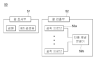
도 3은 본 발명에 따른 모니터링 유닛의 블록도이다.
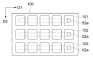
도 4는 도 1의 A부분의 평면도이다.
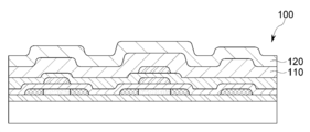
도 5는 연마 전 기판의 단면도이다.
도 6은 연마 후 기판의 단면도이다.
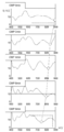
도 7은 연마 정도에 따른 반사광의 스펙트럼을 나타낸 도면이다.
도 8은 본 발명에 따른 두께-스펙트럼 데이터 베이스 생성 방법의 순서도이다.
도 9는 본 발명에 따른 연마 모니터링 방법의 순서도이다.
30: 세정 유닛 40: 건조 유닛
50: 모니터링 유닛 60: 제어 유닛
70: 두께-스펙트럼 데이터 베이스
Claims (20)
- 적어도 하나의 무기막을 포함하는 기판을 제1 방향을 따라 이동시키는 기판 이동 유닛;
상기 기판 이동 유닛 상에 배치된 연마 유닛;
상기 기판 이동 유닛 상에 배치된 세정 유닛 및 건조 유닛;
상기 기판 이동 유닛 상에 배치되고 기판의 서로 다른 복수의 위치의 반사광을 각각 측정하는 복수의 광학 프로브를 포함하는 모니터링 유닛;
상기 연마 유닛, 상기 세정 유닛, 상기 건조 유닛 및 모니터링 유닛은 상기 제1 방향을 따라 순차적으로 배치된 연마 모니터링 시스템. - 제1항에 있어서,
상기 복수의 광학 프로브는 상기 제1 방향과 수직하는 제2 방향을 따라 서로 이격되어 배열된 연마 모니터링 시스템. - 제1항에 있어서,
상기 복수의 광학 프로브는 상기 제1 방향 및 상기 제1 방향과 수직하는 제2 방향에 따라 배열된 복수의 셀을 포함하는 기판의 각 셀에 대응하도록 배치된 연마 모니터링 시스템. - 제1항에 있어서,
상기 무기막의 두께 및 상기 무기막의 두께와 대응하는 기준 스펙트럼으로 이루어진 데이터를 포함하는 두께-스펙트럼 데이터 베이스를 포함하는 연마 모니터링 시스템. - 제4항에 있어서,
상기 두께-스펙트럼 데이터 베이스는 상기 무기막의 두께에 대응하는 연마 시간에 대한 데이터를 포함하는 연마 모니터링 시스템. - 제4항에 있어서,
상기 복수의 광학 프로브와 연결되고, 상기 복수의 광학 프로브로부터 각각 측정된 반사광으로부터 스펙트럼을 각각 산출하는 다중 채널 분광기를 포함하는 연마 모니터링 시스템. - 제6항에 있어서,
상기 산출된 복수의 스펙트럼을 상기 기준 스펙트럼과 비교하는 제어 유닛을 더 포함하는 연마 모니터링 시스템. - 제7항에 있어서,
상기 제어 유닛은 상기 다중 채널 분광기로부터 산출된 스펙트럼의 피크(peak)점 및 밸리(valley)점에서의 파장과 상기 기준 스펙트럼의 피크점 및 밸리점에서의 파장을 각각 비교하는 연마 모니터링 시스템. - 제7항에 있어서,
상기 제어 유닛은 상기 산출된 복수의 스펙트럼을 서로 비교하는 연마 모니터링 시스템. - 두께-스펙트럼 데이터 베이스 생성하는 단계;
적어도 하나의 무기막을 포함하는 기판에 대해 연마 공정을 진행하는 단계;
상기 기판의 서로 다른 복수의 위치에 대해 동시에 각각의 스펙트럼을 산출하는 단계;
상기 산출된 각각의 스펙트럼과 두께-스펙트럼 데이터 베이스에 포함된 기준 스펙트럼과 비교하는 단계;
상기 기판의 서로 다른 복수의 위치에 대한 무기막의 두께를 각각 산출하는 단계; 및
상기 기판의 서로 다른 복수의 위치에 대한 무기막의 두께의 적절성을 판단하는 단계;를 포함하는 연마 모니터링 방법. - 제10항에 있어서,
상기 기판의 서로 다른 복수의 위치에 대해 동시에 각각의 스펙트럼을 산출하는 단계는,
상기 기판의 서로 다른 복수의 위치는 상기 기판에 포함된 복수의 셀에 각각 대응하는 연마 모니터링 방법. - 제10항에 있어서,
상기 기판의 서로 다른 위치에 대한 무기막의 두께의 적절성을 판단하는 단계는,
상기 기판의 서로 다른 위치에 대해 산출된 각각의 두께를 서로 비교하는 단계; 및
상기 무기막의 균일성을 판단하는 단계;를 포함하는 연마 모니터링 방법. - 제10항에 있어서,
상기 두께-스펙트럼 데이터 베이스는 상기 무기막의 두께 및 상기 무기막의 두께와 대응하는 기준 스펙트럼에 대한 데이터를 포함하는 연마 모니터링 방법. - 제10항에 있어서,
상기 두께-스펙트럼 데이터 베이스는 상기 무기막의 두께에 대응하는 연마 시간에 대한 데이터를 포함하는 연마 모니터링 방법. - 제10항에 있어서,
상기 기판의 서로 다른 복수의 위치에 대해 동시에 각각의 스펙트럼을 산출하는 단계는,
상기 기판의 서로 다른 복수의 위치에서 상기 기판의 반사광을 각각 측정하는 단계; 및
상기 각각 측정된 기판의 반사광을 파장에 따라 분해하는 단계;를 포함하는 연마 모니터링 방법. - 제10항에 있어서,
상기 산출된 각각의 스펙트럼과 두께-스펙트럼 데이터 베이스에 포함된 기준 스펙트럼과 비교하는 단계는,
각각 산출된 스펙트럼의 피크(peak)점 및 밸리(valley)점에서의 파장과 상기 기준 스펙트럼의 피크점 및 밸리점에서의 파장을 각각 비교하는 단계;를 더 포함하는 연마 모니터링 방법. - 제10항에 있어서,
상기 기판의 서로 다른 복수의 위치에 대해 동시에 각각의 스펙트럼을 산출하는 단계는,
상기 각각 측정된 반사광을 400nm 이상 900nm 이하의 파장에 따라 광도를 측정하는 연마 모니터링 방법. - 제10항에 있어서,
상기 두께-스펙트럼 데이터 베이스를 생성하는 단계는,
적어도 하나의 무기막을 포함하는 복수의 기판에 대해 연마 공정을 각각 진행하는 단계;
상기 복수의 기판 중 각각의 기판에 대한 스펙트럼을 산출하는 단계;
상기 복수의 기판 중 각각의 기판의 상기 무기막의 두께를 투과 전자 현미경을 통해 측정하는 단계; 및
상기 무기막의 두께 및 상기 무기막의 두께에 대응하는 각각의 기판에 대한 기준 스펙트럼을 산출하는 단계;를 포함하는 연마 모니터링 방법. - 적어도 하나의 무기막을 포함하는 복수의 기판에 대해 연마 공정을 각각 진행하는 단계;
상기 복수의 기판 중 각각의 기판에 대한 스펙트럼을 산출하는 단계;
상기 복수의 기판 중 각각의 기판의 무기막의 두께를 투과 전자 현미경을 통해 측정하는 단계; 및
상기 무기막의 두께 및 상기 무기막의 두께에 대응하는 각각의 기판에 대한 기준 스펙트럼을 산출하는 단계; 를 포함하는 연마 모니터링 방법. - 제19항에 있어서,
상기 무기막의 두께 및 상기 무기막의 두께에 대응하는 각각의 기판에 대한 기준 스펙트럼을 산출하는 단계는,
상기 무기막의 두께에 대응하는 상기 기준 스펙트럼의 피크(peak)점 및 밸리(valley)점에서의 파장을 산출하는 단계;를 포함하는 연마 모니터링 방법.
Priority Applications (3)
| Application Number | Priority Date | Filing Date | Title |
|---|---|---|---|
| KR1020180155045A KR20200068785A (ko) | 2018-12-05 | 2018-12-05 | 연마 모니터링 시스템 및 연마 모니터링 방법 |
| US16/582,658 US20200180103A1 (en) | 2018-12-05 | 2019-09-25 | Apparatus and method for monitoring chemical mechanical polishing |
| CN201911233241.XA CN111267000A (zh) | 2018-12-05 | 2019-12-05 | 用于监测抛光的设备和方法 |
Applications Claiming Priority (1)
| Application Number | Priority Date | Filing Date | Title |
|---|---|---|---|
| KR1020180155045A KR20200068785A (ko) | 2018-12-05 | 2018-12-05 | 연마 모니터링 시스템 및 연마 모니터링 방법 |
Publications (1)
| Publication Number | Publication Date |
|---|---|
| KR20200068785A true KR20200068785A (ko) | 2020-06-16 |
Family
ID=70970595
Family Applications (1)
| Application Number | Title | Priority Date | Filing Date |
|---|---|---|---|
| KR1020180155045A Ceased KR20200068785A (ko) | 2018-12-05 | 2018-12-05 | 연마 모니터링 시스템 및 연마 모니터링 방법 |
Country Status (3)
| Country | Link |
|---|---|
| US (1) | US20200180103A1 (ko) |
| KR (1) | KR20200068785A (ko) |
| CN (1) | CN111267000A (ko) |
Cited By (1)
| Publication number | Priority date | Publication date | Assignee | Title |
|---|---|---|---|---|
| CN113560962A (zh) * | 2021-07-28 | 2021-10-29 | 安徽鸿海新材料股份有限公司 | 一种厚度极差较优异的覆铜板制备方法 |
Families Citing this family (3)
| Publication number | Priority date | Publication date | Assignee | Title |
|---|---|---|---|---|
| KR20200130545A (ko) * | 2019-05-08 | 2020-11-19 | 삼성디스플레이 주식회사 | 표시 장치의 제조장치 및 표시 장치의 제조방법 |
| CN112355849A (zh) * | 2020-10-15 | 2021-02-12 | 深圳市鑫达辉软性电路科技有限公司 | 一种物理型氧化清洗机 |
| CN118376184B (zh) * | 2024-03-11 | 2024-11-19 | 江苏西欧电子有限公司 | 一种用于电能表原料加工的光滑处理检测装置 |
Family Cites Families (17)
| Publication number | Priority date | Publication date | Assignee | Title |
|---|---|---|---|---|
| JPH0199229A (ja) * | 1987-10-13 | 1989-04-18 | Nec Corp | 半導体ウェハーのベルト式搬送装置 |
| US6111634A (en) * | 1997-05-28 | 2000-08-29 | Lam Research Corporation | Method and apparatus for in-situ monitoring of thickness using a multi-wavelength spectrometer during chemical-mechanical polishing |
| US6273796B1 (en) * | 1999-09-01 | 2001-08-14 | Micron Technology, Inc. | Method and apparatus for planarizing a microelectronic substrate with a tilted planarizing surface |
| US6270620B1 (en) * | 1999-09-14 | 2001-08-07 | World Wiser Electronics Inc. | Etching device |
| JP3854056B2 (ja) * | 1999-12-13 | 2006-12-06 | 株式会社荏原製作所 | 基板膜厚測定方法、基板膜厚測定装置、基板処理方法及び基板処理装置 |
| US6447374B1 (en) * | 1999-12-17 | 2002-09-10 | Applied Materials, Inc. | Chemical mechanical planarization system |
| US6616801B1 (en) * | 2000-03-31 | 2003-09-09 | Lam Research Corporation | Method and apparatus for fixed-abrasive substrate manufacturing and wafer polishing in a single process path |
| ATE313412T1 (de) * | 2001-06-26 | 2006-01-15 | Lam Res Corp | System zur endpunktbestimmung beim chemisch- mechanischen polieren |
| US6562185B2 (en) * | 2001-09-18 | 2003-05-13 | Advanced Micro Devices, Inc. | Wafer based temperature sensors for characterizing chemical mechanical polishing processes |
| KR100808829B1 (ko) * | 2002-12-26 | 2008-03-07 | 램 리써치 코포레이션 | 화학기계적 연마 시스템, 웨이퍼 표면의 프로세스 상태 모니터링 방법, 및 엔드포인트 검출 방법 |
| JP4863726B2 (ja) * | 2006-02-03 | 2012-01-25 | 株式会社リコー | 定着装置、画像形成装置 |
| JP5612945B2 (ja) * | 2010-07-23 | 2014-10-22 | 株式会社荏原製作所 | 基板の研磨の進捗を監視する方法および研磨装置 |
| JP5980476B2 (ja) * | 2010-12-27 | 2016-08-31 | 株式会社荏原製作所 | ポリッシング装置およびポリッシング方法 |
| JP5798505B2 (ja) * | 2011-04-27 | 2015-10-21 | 株式会社Screenホールディングス | 基板処理装置および基板処理方法 |
| US9067295B2 (en) * | 2012-07-25 | 2015-06-30 | Applied Materials, Inc. | Monitoring retaining ring thickness and pressure control |
| WO2015163164A1 (ja) * | 2014-04-22 | 2015-10-29 | 株式会社 荏原製作所 | 研磨方法および研磨装置 |
| CN106217232B (zh) * | 2016-08-31 | 2018-08-17 | 广州创芯旗自动化控制设备有限公司 | 一种超精密研磨机 |
-
2018
- 2018-12-05 KR KR1020180155045A patent/KR20200068785A/ko not_active Ceased
-
2019
- 2019-09-25 US US16/582,658 patent/US20200180103A1/en not_active Abandoned
- 2019-12-05 CN CN201911233241.XA patent/CN111267000A/zh active Pending
Cited By (1)
| Publication number | Priority date | Publication date | Assignee | Title |
|---|---|---|---|---|
| CN113560962A (zh) * | 2021-07-28 | 2021-10-29 | 安徽鸿海新材料股份有限公司 | 一种厚度极差较优异的覆铜板制备方法 |
Also Published As
| Publication number | Publication date |
|---|---|
| CN111267000A (zh) | 2020-06-12 |
| US20200180103A1 (en) | 2020-06-11 |
Similar Documents
| Publication | Publication Date | Title |
|---|---|---|
| KR102808528B1 (ko) | Cmp 프로세스 제어 알고리즘에 대한 입력으로서의 기계 시각 | |
| KR102741434B1 (ko) | 분광 모니터링을 위한 기계 학습 시스템을 위한 훈련 스펙트럼 생성 | |
| US9969048B2 (en) | Polishing apparatus | |
| US7840375B2 (en) | Methods and apparatus for generating a library of spectra | |
| CN116833898B (zh) | 使用神经网络的光谱监测 | |
| KR20200068785A (ko) | 연마 모니터링 시스템 및 연마 모니터링 방법 | |
| KR101669554B1 (ko) | 기판 폴리싱의 진행을 감시하는 방법 및 폴리싱장치 | |
| US8951813B2 (en) | Method of polishing a substrate having a film on a surface of the substrate for semiconductor manufacturing | |
| KR100305537B1 (ko) | 연마방법및그것을사용한연마장치 | |
| TWI602644B (zh) | 在研磨期間使用攝影機的反射量測 | |
| US20150017880A1 (en) | Film-thickness measuring apparatus, film-thickness measuring method, and polishing apparatus having the film-thickness measuring apparatus | |
| US20070224915A1 (en) | Substrate thickness measuring during polishing | |
| US20190027382A1 (en) | Substrate polishing apparatus and method | |
| KR102678211B1 (ko) | 프레스톤 행렬 생성기 | |
| US9056383B2 (en) | Path for probe of spectrographic metrology system | |
| JP6292819B2 (ja) | 選択的スペクトルモニタリングを使用した終点決定 | |
| JPH09298176A (ja) | 研磨方法及びそれを用いた研磨装置 | |
| US10978321B2 (en) | Method and system for processing patterned structures | |
| JPH09298174A (ja) | 研磨方法及びそれを用いた研磨装置 | |
| US20140242877A1 (en) | Spectrographic metrology with multiple measurements | |
| US20250153309A1 (en) | Signal processing for finding substrate notch | |
| US20250108474A1 (en) | Finding substrate notch on substrate between platens in chemical mechanical polishing | |
| JPH09298175A (ja) | 研磨方法及びそれを用いた研磨装置 | |
| JP2024158390A (ja) | 研磨方法、コンピュータを動作させるためのプログラム、および研磨装置 |
Legal Events
| Date | Code | Title | Description |
|---|---|---|---|
| PA0109 | Patent application |
St.27 status event code: A-0-1-A10-A12-nap-PA0109 |
|
| R18-X000 | Changes to party contact information recorded |
St.27 status event code: A-3-3-R10-R18-oth-X000 |
|
| R17-X000 | Change to representative recorded |
St.27 status event code: A-3-3-R10-R17-oth-X000 |
|
| PG1501 | Laying open of application |
St.27 status event code: A-1-1-Q10-Q12-nap-PG1501 |
|
| A201 | Request for examination | ||
| PA0201 | Request for examination |
St.27 status event code: A-1-2-D10-D11-exm-PA0201 |
|
| D13-X000 | Search requested |
St.27 status event code: A-1-2-D10-D13-srh-X000 |
|
| D14-X000 | Search report completed |
St.27 status event code: A-1-2-D10-D14-srh-X000 |
|
| E902 | Notification of reason for refusal | ||
| PE0902 | Notice of grounds for rejection |
St.27 status event code: A-1-2-D10-D21-exm-PE0902 |
|
| AMND | Amendment | ||
| E13-X000 | Pre-grant limitation requested |
St.27 status event code: A-2-3-E10-E13-lim-X000 |
|
| P11-X000 | Amendment of application requested |
St.27 status event code: A-2-2-P10-P11-nap-X000 |
|
| P13-X000 | Application amended |
St.27 status event code: A-2-2-P10-P13-nap-X000 |
|
| E601 | Decision to refuse application | ||
| PE0601 | Decision on rejection of patent |
St.27 status event code: N-2-6-B10-B15-exm-PE0601 |
|
| X091 | Application refused [patent] | ||
| AMND | Amendment | ||
| E13-X000 | Pre-grant limitation requested |
St.27 status event code: A-2-3-E10-E13-lim-X000 |
|
| P11-X000 | Amendment of application requested |
St.27 status event code: A-2-2-P10-P11-nap-X000 |
|
| P13-X000 | Application amended |
St.27 status event code: A-2-2-P10-P13-nap-X000 |
|
| PX0901 | Re-examination |
St.27 status event code: A-2-3-E10-E12-rex-PX0901 |
|
| PX0601 | Decision of rejection after re-examination |
St.27 status event code: N-2-6-B10-B17-rex-PX0601 |
|
| X601 | Decision of rejection after re-examination | ||
| P22-X000 | Classification modified |
St.27 status event code: A-2-2-P10-P22-nap-X000 |