US5883395A - Monolithic, multiple-channel optical coupler - Google Patents
Monolithic, multiple-channel optical coupler Download PDFInfo
- Publication number
- US5883395A US5883395A US08/933,795 US93379597A US5883395A US 5883395 A US5883395 A US 5883395A US 93379597 A US93379597 A US 93379597A US 5883395 A US5883395 A US 5883395A
- Authority
- US
- United States
- Prior art keywords
- set forth
- detecting
- coupler
- light
- common
- Prior art date
- Legal status (The legal status is an assumption and is not a legal conclusion. Google has not performed a legal analysis and makes no representation as to the accuracy of the status listed.)
- Expired - Fee Related
Links
- 230000003287 optical effect Effects 0.000 title claims abstract description 24
- 239000000758 substrate Substances 0.000 claims abstract description 14
- 239000004065 semiconductor Substances 0.000 claims abstract description 6
- 230000037361 pathway Effects 0.000 claims description 4
- 230000009977 dual effect Effects 0.000 claims description 2
- 238000010586 diagram Methods 0.000 description 3
- 235000012431 wafers Nutrition 0.000 description 3
- 230000008878 coupling Effects 0.000 description 2
- 238000010168 coupling process Methods 0.000 description 2
- 238000005859 coupling reaction Methods 0.000 description 2
- 238000002955 isolation Methods 0.000 description 2
- 238000004806 packaging method and process Methods 0.000 description 2
- JBRZTFJDHDCESZ-UHFFFAOYSA-N AsGa Chemical compound [As]#[Ga] JBRZTFJDHDCESZ-UHFFFAOYSA-N 0.000 description 1
- 229910001218 Gallium arsenide Inorganic materials 0.000 description 1
- 229920004142 LEXAN™ Polymers 0.000 description 1
- 230000003321 amplification Effects 0.000 description 1
- 230000004888 barrier function Effects 0.000 description 1
- 230000005670 electromagnetic radiation Effects 0.000 description 1
- 230000006872 improvement Effects 0.000 description 1
- 238000004519 manufacturing process Methods 0.000 description 1
- 239000000463 material Substances 0.000 description 1
- 238000012986 modification Methods 0.000 description 1
- 230000004048 modification Effects 0.000 description 1
- 238000003199 nucleic acid amplification method Methods 0.000 description 1
- 230000005693 optoelectronics Effects 0.000 description 1
Images


Classifications
-
- H—ELECTRICITY
- H10—SEMICONDUCTOR DEVICES; ELECTRIC SOLID-STATE DEVICES NOT OTHERWISE PROVIDED FOR
- H10F—INORGANIC SEMICONDUCTOR DEVICES SENSITIVE TO INFRARED RADIATION, LIGHT, ELECTROMAGNETIC RADIATION OF SHORTER WAVELENGTH OR CORPUSCULAR RADIATION
- H10F55/00—Radiation-sensitive semiconductor devices covered by groups H10F10/00, H10F19/00 or H10F30/00 being structurally associated with electric light sources and electrically or optically coupled thereto
- H10F55/20—Radiation-sensitive semiconductor devices covered by groups H10F10/00, H10F19/00 or H10F30/00 being structurally associated with electric light sources and electrically or optically coupled thereto wherein the electric light source controls the radiation-sensitive semiconductor devices, e.g. optocouplers
- H10F55/25—Radiation-sensitive semiconductor devices covered by groups H10F10/00, H10F19/00 or H10F30/00 being structurally associated with electric light sources and electrically or optically coupled thereto wherein the electric light source controls the radiation-sensitive semiconductor devices, e.g. optocouplers wherein the radiation-sensitive devices and the electric light source are all semiconductor devices
- H10F55/255—Radiation-sensitive semiconductor devices covered by groups H10F10/00, H10F19/00 or H10F30/00 being structurally associated with electric light sources and electrically or optically coupled thereto wherein the electric light source controls the radiation-sensitive semiconductor devices, e.g. optocouplers wherein the radiation-sensitive devices and the electric light source are all semiconductor devices formed in, or on, a common substrate
-
- H—ELECTRICITY
- H10—SEMICONDUCTOR DEVICES; ELECTRIC SOLID-STATE DEVICES NOT OTHERWISE PROVIDED FOR
- H10F—INORGANIC SEMICONDUCTOR DEVICES SENSITIVE TO INFRARED RADIATION, LIGHT, ELECTROMAGNETIC RADIATION OF SHORTER WAVELENGTH OR CORPUSCULAR RADIATION
- H10F77/00—Constructional details of devices covered by this subclass
- H10F77/30—Coatings
- H10F77/306—Coatings for devices having potential barriers
- H10F77/331—Coatings for devices having potential barriers for filtering or shielding light, e.g. multicolour filters for photodetectors
- H10F77/334—Coatings for devices having potential barriers for filtering or shielding light, e.g. multicolour filters for photodetectors for shielding light, e.g. light blocking layers or cold shields for infrared detectors
Definitions
- This invention generally relates to optical couplers. Specifically, the invention is directed to a monolithic multiple channel optical coupler.
- Existing optical couplers generally exhibit a variation in performance from device to device. For example, the current transfer ratio and speed of an optical device can vary significantly. This can pose a significant problem when one is coupling multiple channels and minimal device-to-device variation is needed to preserve relative channel signal levels.
- Couplers Part of the problem can be minimized by using multiple channel couplers.
- the individual optical devices within such couplers may be fabricated from different wafers or different portions of the same wafer, they are not necessarily matched devices. Further, such couplers may not use isolated optical paths for the devices to minimize cross-talk. Thus, even within one package, performance variations persist.
- coupler that can handle multiple signals with minimal channel-to-channel variation in signal transfer performance. Also, it is desirable to provide a coupler that has the maximum number of isolated channels using the least number of pins, to reduce assembly costs and to reduce the required printed circuit board space.
- a monolithic-detector, multiple-channel optical coupler having common LED-emitter cathodes and common photodetector collectors, or having common LED-emitter anodes and common photodetector emitters.
- the photodetectors are contained on a single, monolithic semiconductor substrate which provides electro-optically matched devices and common connections for the devices. Although the individual coupling devices share electrical commonality, they are optically isolated by the use of a light pipe arrangement between the LED-emitters and the photodetectors. Moreover, pin count is minimized by using common connections for the LED-emitters and the photodetectors.
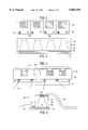
- FIG. 1 is an electrical schematic diagram of a monolithic-detector, multiple-channel optical coupler constructed in accordance with the present invention
- FIG. 2 is a top-view of a substrate containing photodetectors of the coupler of FIG. 1;
- FIG. 3 is a front-elevation partial assembly view of the coupler of FIG. 1;
- FIG. 4 is a top partial-assembly view of the coupler of FIG. 1;
- FIG. 5 is a side elevation assembly view of the coupler of FIG. 1;
- FIG. 6 is an alternative electrical schematic diagram of a monolithic-detector.
- the emitters and photodetectors described here are of the kind discussed in the Siemens Optoelectronics Data Book 1993. It should be understood that other devices can be used as well. Also, the coupler could be used with other types of electromagnetic radiation, such as ultraviolet light.
- a monolithic-detector, multiple-channel optical coupler 10 is shown in the electrical schematic diagram of FIG. 1.
- the coupler 10 shown here is contained in a dual in-line package 12 having ten pins 14, but could be held in any other suitable packaging device.
- the coupler 10 has four gallium arsenide LED (light emitting diode) emitters 20 (or some other suitable emitter), each having an anode 22 and a cathode 24 with the cathodes 24 tied to a first common bus 26, and four photodetectors 40, each having a collector 42, an emitter 44, and a base 46, with the collectors 42 tied to a second common bus 48.
- Each LED-emitter 20/photodetector 40 pair is used to couple one signal channel for the coupler 10.
- the number four is arbitrary; any number of devices could be provided. Also, one could commonly connect the anodes 22 of the LED emitters 20 instead of the cathodes 24 and similarly connect the emitters 44 instead of the collectors 42 of the photodetectors 40, as shown in FIG. 6. Moreover, one could use photodiodes instead of the depicted phototransistors for the photodetectors 40. Finally, if the application required it, one could choose to bring out from the package 12 individual leads for every device, i.e., every LED emitter and photodetector.
- the anodes 22 of the LED emitters 20 and the emitters 44 of the photodetectors 40 are each connected to individual pins 14.
- the common buses 26 and 48 for the cathodes 24 and the collectors 42, respectively, are also connected to separate pins 14 of the package 12.
- individual cathode 24 and/or collector 42 connections could be provided.
- FIGS. 2 through 5 The physical structure of the coupler 10 is illustrated in FIGS. 2 through 5.
- a monolithic semiconductor substrate 60 having four photodetectors 40 is shown.
- a photodetector region 62 for each photodetector 40 and connecting pads 64 for each associated emitter 44 is visible in this view. Because the four devices come from adjacent portions of the same wafer and their characteristics are thus nearly the same, this arrangement offers nearest neighbor matching of performance or operating characteristics.
- FIG. 3 A front-elevation partial assembly view of the coupler 10 is shown in FIG. 3.
- the substrate 60 is located on a mounting base 70.
- An opaque shield 80 fabricated from an opaque material, for example, white Lexan®, is positioned over the substrate 60. White is preferable because it reflects light.
- Within the shield 80 are formed respective light pipes 90 for the passage of light to the photodetector regions 62.
- the light pipes 90 have an inward taper 92 from the substrate 60 upwards to minimize cross talk between the channels formed thereby.
- FIG. 4 A top partial-assembly view of the coupler 10 is shown in FIG. 4.
- electrically-conductive wires 110 connected to the pads 64 for the emitters 44 of the photodetectors 40.
- the wires 110 are each connected to individual pins 14 of the coupler package 12.
- FIG. 5 a side elevation assembly view of the coupler 10, an electrically-conductive wire 120 is shown connected to the anode 22 of an LED emitter 20. Similar wires 120 are connected to the anodes 22 of the other LED emitters 20. As indicated above, the wires 120 are each connected to individual pins 14 of the coupler package 12. Note that the LED emitter 20 is positioned at the tapered end of the light pipe 90 and opposite the respective photodetector region 62. The other LED emitters 20 are similarly positioned at the other light pipes 90 so that each LED emitter 20 is paired with a respective photodetector region 62 via an individual light pipe 90.
- the coupler 10 In actual manufacture of the coupler 10, one could choose to use a detector strip or sheet die attached in one operation on a common lead frame pad or with individual lead frame connections. Also, the individual photodetector region 62/emitter 44 pairs need not be arranged in a line but could be configured in a square or any other desired arrangement that provides electro-optically matched photodetectors 60.
- the optical coupler 10 is used to transmit signal information between respective circuitry while maintaining electrical isolation therebetween. This is accomplished since optical signals, and not electrical signals, are passed between the LED-emitters 20 and the photodetectors 40 which are connected to respective portions of the circuitry.
- the common collector arrangement of the photodetectors 40 results in a non-inverting amplification of the optical signal received from the LED-emitters 20.
- the light emitted to the respective photodetector 40 will cause the output of the photodetector 40 to be at a high voltage level.
- the output of the photodetector 40 is connected to the remainder of the circuitry.
- the output of the photodetector 40 will be at a low voltage level.
- the light pipes 90 ensure that the light pathway between a respective LED emitter 20 and photodetector 40 is isolated from the other light pathways. As a result, no mixing of optical signals occurs (i.e., no cross talk occurs) and each photodetector 40 receives only one optical signal. Note that, in data communications applications, all signals can be referenced to a common ground on either side of the isolation barrier.
- the coupler 10 achieves an improved channel density per pin count by the use of the common connections of the LED emitters 20 and the photodetectors 40 in lieu of bringing out separate leads for each device.
- the number of pins required for the common connections is two plus twice the number of channels to be coupled.
- the number of required pins equals ten. This is in contrast to presently available four-channel couplers that require sixteen pins and, thus, a much larger package.
- the coupler 10 achieves this improvement in pin count and packaging while increasing performance.
Landscapes
- Photo Coupler, Interrupter, Optical-To-Optical Conversion Devices (AREA)
Priority Applications (1)
| Application Number | Priority Date | Filing Date | Title |
|---|---|---|---|
| US08/933,795 US5883395A (en) | 1993-09-23 | 1997-09-19 | Monolithic, multiple-channel optical coupler |
Applications Claiming Priority (3)
| Application Number | Priority Date | Filing Date | Title |
|---|---|---|---|
| US12594593A | 1993-09-23 | 1993-09-23 | |
| US59733996A | 1996-02-06 | 1996-02-06 | |
| US08/933,795 US5883395A (en) | 1993-09-23 | 1997-09-19 | Monolithic, multiple-channel optical coupler |
Related Parent Applications (1)
| Application Number | Title | Priority Date | Filing Date |
|---|---|---|---|
| US59733996A Continuation | 1993-09-23 | 1996-02-06 |
Publications (1)
| Publication Number | Publication Date |
|---|---|
| US5883395A true US5883395A (en) | 1999-03-16 |
Family
ID=22422179
Family Applications (1)
| Application Number | Title | Priority Date | Filing Date |
|---|---|---|---|
| US08/933,795 Expired - Fee Related US5883395A (en) | 1993-09-23 | 1997-09-19 | Monolithic, multiple-channel optical coupler |
Country Status (2)
| Country | Link |
|---|---|
| US (1) | US5883395A (fr) |
| EP (1) | EP0645826A3 (fr) |
Cited By (6)
| Publication number | Priority date | Publication date | Assignee | Title |
|---|---|---|---|---|
| US6093938A (en) * | 1999-05-25 | 2000-07-25 | Intel Corporation | Stacked die integrated circuit device |
| US20040202442A1 (en) * | 2003-04-11 | 2004-10-14 | Atsushi Murayama | Multichannel photocoupler |
| US20070071390A1 (en) * | 2005-09-26 | 2007-03-29 | Tobiason Joseph D | Fiber-optic alignment with detector IC |
| US8274657B2 (en) | 2006-11-30 | 2012-09-25 | Osram Opto Semiconductors Gmbh | Radiation detector |
| US20130278064A1 (en) * | 2011-10-19 | 2013-10-24 | Creative Electron, Inc. | Ultra-Low Noise, High Voltage, Adjustable DC-DC Converter Using Photoelectric Effect |
| JP2017112538A (ja) * | 2015-12-17 | 2017-06-22 | 株式会社東芝 | 光結合装置 |
Citations (14)
| Publication number | Priority date | Publication date | Assignee | Title |
|---|---|---|---|---|
| US3413480A (en) * | 1963-11-29 | 1968-11-26 | Texas Instruments Inc | Electro-optical transistor switching device |
| EP0084621A2 (fr) * | 1982-01-22 | 1983-08-03 | International Business Machines Corporation | Convertisseur de signaux à semi-conducteur utilisant le photoncouplage |
| US4695120A (en) * | 1985-09-26 | 1987-09-22 | The United States Of America As Represented By The Secretary Of The Army | Optic-coupled integrated circuits |
| US4847507A (en) * | 1988-01-19 | 1989-07-11 | John Fluke Mfg. Co., Inc. | Fiber optic guard crossing of circuits having analog and digital sections |
| US4989935A (en) * | 1988-09-30 | 1991-02-05 | Siemens Aktiengesellschaft | Optoelectronic transmitter and receiver |
| EP0416284A1 (fr) * | 1989-09-07 | 1991-03-13 | Siemens Aktiengesellschaft | Coupleur optique |
| EP0463390A2 (fr) * | 1990-06-22 | 1992-01-02 | International Business Machines Corporation | Connecteurs électro-optiques |
| US5089948A (en) * | 1990-06-29 | 1992-02-18 | Digital Equipment Corporation | High speed optoisolator switching apparatus |
| DE4133773A1 (de) * | 1990-10-12 | 1992-04-16 | Sharp Kk | Optoelektronische einrichtung, metallform zur herstellung der optoelektronischen einrichtung und verfahren zur herstellung der optoelektronischen einrichtung unter verwendung der metallform |
| US5287376A (en) * | 1992-12-14 | 1994-02-15 | Xerox Corporation | Independently addressable semiconductor diode lasers with integral lowloss passive waveguides |
| US5332894A (en) * | 1992-05-06 | 1994-07-26 | Nec Corporation | Optical output control IC and optical input amplifier IC |
| US5340993A (en) * | 1993-04-30 | 1994-08-23 | Motorola, Inc. | Optocoupler package wth integral voltage isolation barrier |
| US5355386A (en) * | 1992-11-17 | 1994-10-11 | Gte Laboratories Incorporated | Monolithically integrated semiconductor structure and method of fabricating such structure |
| US5424573A (en) * | 1992-03-04 | 1995-06-13 | Hitachi, Ltd. | Semiconductor package having optical interconnection access |
-
1994
- 1994-09-14 EP EP94114455A patent/EP0645826A3/fr not_active Ceased
-
1997
- 1997-09-19 US US08/933,795 patent/US5883395A/en not_active Expired - Fee Related
Patent Citations (16)
| Publication number | Priority date | Publication date | Assignee | Title |
|---|---|---|---|---|
| US3413480A (en) * | 1963-11-29 | 1968-11-26 | Texas Instruments Inc | Electro-optical transistor switching device |
| EP0084621A2 (fr) * | 1982-01-22 | 1983-08-03 | International Business Machines Corporation | Convertisseur de signaux à semi-conducteur utilisant le photoncouplage |
| US4695120A (en) * | 1985-09-26 | 1987-09-22 | The United States Of America As Represented By The Secretary Of The Army | Optic-coupled integrated circuits |
| US4847507A (en) * | 1988-01-19 | 1989-07-11 | John Fluke Mfg. Co., Inc. | Fiber optic guard crossing of circuits having analog and digital sections |
| US4989935A (en) * | 1988-09-30 | 1991-02-05 | Siemens Aktiengesellschaft | Optoelectronic transmitter and receiver |
| EP0416284A1 (fr) * | 1989-09-07 | 1991-03-13 | Siemens Aktiengesellschaft | Coupleur optique |
| US5093879A (en) * | 1990-06-22 | 1992-03-03 | International Business Machines Corporation | Electro-optical connectors |
| EP0463390A2 (fr) * | 1990-06-22 | 1992-01-02 | International Business Machines Corporation | Connecteurs électro-optiques |
| US5089948A (en) * | 1990-06-29 | 1992-02-18 | Digital Equipment Corporation | High speed optoisolator switching apparatus |
| DE4133773A1 (de) * | 1990-10-12 | 1992-04-16 | Sharp Kk | Optoelektronische einrichtung, metallform zur herstellung der optoelektronischen einrichtung und verfahren zur herstellung der optoelektronischen einrichtung unter verwendung der metallform |
| US5245198A (en) * | 1990-10-12 | 1993-09-14 | Sharp Kabushiki Kaisha | Optoelectronic device, metal mold for manufacturing the device and manufacturing method of the device using the metal mold |
| US5424573A (en) * | 1992-03-04 | 1995-06-13 | Hitachi, Ltd. | Semiconductor package having optical interconnection access |
| US5332894A (en) * | 1992-05-06 | 1994-07-26 | Nec Corporation | Optical output control IC and optical input amplifier IC |
| US5355386A (en) * | 1992-11-17 | 1994-10-11 | Gte Laboratories Incorporated | Monolithically integrated semiconductor structure and method of fabricating such structure |
| US5287376A (en) * | 1992-12-14 | 1994-02-15 | Xerox Corporation | Independently addressable semiconductor diode lasers with integral lowloss passive waveguides |
| US5340993A (en) * | 1993-04-30 | 1994-08-23 | Motorola, Inc. | Optocoupler package wth integral voltage isolation barrier |
Cited By (8)
| Publication number | Priority date | Publication date | Assignee | Title |
|---|---|---|---|---|
| US6093938A (en) * | 1999-05-25 | 2000-07-25 | Intel Corporation | Stacked die integrated circuit device |
| US6229158B1 (en) * | 1999-05-25 | 2001-05-08 | Intel Corporation | Stacked die integrated circuit device |
| US20040202442A1 (en) * | 2003-04-11 | 2004-10-14 | Atsushi Murayama | Multichannel photocoupler |
| US20070071390A1 (en) * | 2005-09-26 | 2007-03-29 | Tobiason Joseph D | Fiber-optic alignment with detector IC |
| US7217041B2 (en) | 2005-09-26 | 2007-05-15 | Mitutoyo Corporation | Fiber-optic alignment with detector IC |
| US8274657B2 (en) | 2006-11-30 | 2012-09-25 | Osram Opto Semiconductors Gmbh | Radiation detector |
| US20130278064A1 (en) * | 2011-10-19 | 2013-10-24 | Creative Electron, Inc. | Ultra-Low Noise, High Voltage, Adjustable DC-DC Converter Using Photoelectric Effect |
| JP2017112538A (ja) * | 2015-12-17 | 2017-06-22 | 株式会社東芝 | 光結合装置 |
Also Published As
| Publication number | Publication date |
|---|---|
| EP0645826A2 (fr) | 1995-03-29 |
| EP0645826A3 (fr) | 1995-05-17 |
Similar Documents
| Publication | Publication Date | Title |
|---|---|---|
| US5122893A (en) | Bi-directional optical transceiver | |
| US4225213A (en) | Connector apparatus | |
| US4533833A (en) | Optically coupled integrated circuit array | |
| JPH01137207A (ja) | 電気−光変換器組立体 | |
| JPH1093131A (ja) | 多方向光結合器 | |
| US20020034351A1 (en) | Electro-optic interconnect circuit board | |
| JPH0642527B2 (ja) | 光導波路を用いた情報処理装置 | |
| US5883395A (en) | Monolithic, multiple-channel optical coupler | |
| US20040081473A1 (en) | Direct attach optical receiver module and method of testing | |
| US4184070A (en) | Connector apparatus | |
| JP3680303B2 (ja) | 光電変換モジュール | |
| EP0738016A2 (fr) | Paire différentielle de thyristors optiques utilisée en tant que transmetteur optoélectronique | |
| EP0646973B1 (fr) | Photocoupleur bidirectionnel linéaire | |
| US5636047A (en) | Optical interconnection system | |
| US6624643B2 (en) | Apparatus and method to read output information from a backside of a silicon device | |
| JPH04307976A (ja) | アレイ光半導体装置 | |
| JPS58168284A (ja) | 多連光結合素子 | |
| JPS6317569A (ja) | 光結合素子 | |
| US20010048695A1 (en) | High speed modulation utilizing field effect for return path | |
| US6552407B1 (en) | Communication module having a structure for reducing crosstalk | |
| JPH11261083A (ja) | 光受信装置 | |
| JPS6068678A (ja) | 光結合半導体装置 | |
| JPH0685432B2 (ja) | 半導体装置 | |
| JPH09283775A (ja) | 光受信器 | |
| JPH07131319A (ja) | フォトカプラ回路及びその装置 |
Legal Events
| Date | Code | Title | Description |
|---|---|---|---|
| FEPP | Fee payment procedure |
Free format text: PAYER NUMBER DE-ASSIGNED (ORIGINAL EVENT CODE: RMPN); ENTITY STATUS OF PATENT OWNER: LARGE ENTITY Free format text: PAYOR NUMBER ASSIGNED (ORIGINAL EVENT CODE: ASPN); ENTITY STATUS OF PATENT OWNER: LARGE ENTITY |
|
| FEPP | Fee payment procedure |
Free format text: PAYOR NUMBER ASSIGNED (ORIGINAL EVENT CODE: ASPN); ENTITY STATUS OF PATENT OWNER: LARGE ENTITY |
|
| FPAY | Fee payment |
Year of fee payment: 4 |
|
| REMI | Maintenance fee reminder mailed | ||
| AS | Assignment |
Owner name: INFINEON TECHNOLOGIES CORPORATION, CALIFORNIA Free format text: CHANGE OF NAME;ASSIGNOR:SIEMENS DRAM SEMICONDUCTOR CORPORATION;REEL/FRAME:014363/0078 Effective date: 19990401 Owner name: INFINEON TECHNOLOGIES NORTH AMERICA CORP., CALIFOR Free format text: CHANGE OF NAME;ASSIGNOR:INFINEON TECHNOLOGIES CORPORATION;REEL/FRAME:014363/0102 Effective date: 19990930 Owner name: SIEMENS DRAM SEMICONDUCTOR CORPORATION, CALIFORNIA Free format text: ASSIGNMENT OF ASSIGNORS INTEREST;ASSIGNOR:SIEMENS MICROELECTRONICS, INC.;REEL/FRAME:014363/0076 Effective date: 19990330 Owner name: VISHAY INFRARED COMPONENTS, CALIFORNIA Free format text: CHANGE OF NAME;ASSIGNOR:INFINEON TECHNOLOGIES NORTH AMERICA CORP.;REEL/FRAME:014363/0081 Effective date: 19990805 |
|
| AS | Assignment |
Owner name: VISHAY INFRARED COMPONENTS, CALIFORNIA Free format text: CORRECTIVE FROM CHANGE OF NAME TO ASSIGNMENT AND CORRECTED ADDRESS.;ASSIGNOR:INFINEON TECHNOLOGIES NORTH AMERICA CORP.;REEL/FRAME:014373/0348 Effective date: 19990805 Owner name: VISHAY INFRARED COMPONENTS, CALIFORNIA Free format text: CORRECTIVE ASSIGNMENT TO CORRECT THE NATURE OF CONVEYANCE AND ASSIGNEE ADDRESS PREVIOUSLY RECORDED AT REEL 014363 FRAME 0081. THE ASSIGNOR HEREBY CONFIRMS THE ASSIGNMENT OF THE ENTIRE INTEREST;ASSIGNOR:INFINEON TECHNOLOGIES NORTH AMERICA CORP.;REEL/FRAME:014373/0348 Effective date: 19990805 |
|
| REMI | Maintenance fee reminder mailed | ||
| LAPS | Lapse for failure to pay maintenance fees | ||
| STCH | Information on status: patent discontinuation |
Free format text: PATENT EXPIRED DUE TO NONPAYMENT OF MAINTENANCE FEES UNDER 37 CFR 1.362 |
|
| FP | Lapsed due to failure to pay maintenance fee |
Effective date: 20070316 |