US6051093A - Mounting method of semiconductor element - Google Patents
Mounting method of semiconductor element Download PDFInfo
- Publication number
- US6051093A US6051093A US09/011,603 US1160398A US6051093A US 6051093 A US6051093 A US 6051093A US 1160398 A US1160398 A US 1160398A US 6051093 A US6051093 A US 6051093A
- Authority
- US
- United States
- Prior art keywords
- semiconductor element
- circuit board
- conductive paste
- protruding bump
- electrode
- Prior art date
- Legal status (The legal status is an assumption and is not a legal conclusion. Google has not performed a legal analysis and makes no representation as to the accuracy of the status listed.)
- Expired - Fee Related
Links
Images


Classifications
-
- H—ELECTRICITY
- H10—SEMICONDUCTOR DEVICES; ELECTRIC SOLID-STATE DEVICES NOT OTHERWISE PROVIDED FOR
- H10W—GENERIC PACKAGES, INTERCONNECTIONS, CONNECTORS OR OTHER CONSTRUCTIONAL DETAILS OF DEVICES COVERED BY CLASS H10
- H10W72/00—Interconnections or connectors in packages
- H10W72/071—Connecting or disconnecting
-
- H—ELECTRICITY
- H05—ELECTRIC TECHNIQUES NOT OTHERWISE PROVIDED FOR
- H05K—PRINTED CIRCUITS; CASINGS OR CONSTRUCTIONAL DETAILS OF ELECTRIC APPARATUS; MANUFACTURE OF ASSEMBLAGES OF ELECTRICAL COMPONENTS
- H05K1/00—Printed circuits
- H05K1/02—Details
- H05K1/11—Printed elements for providing electric connections to or between printed circuits
- H05K1/111—Pads for surface mounting, e.g. lay-out
- H05K1/112—Pads for surface mounting, e.g. lay-out directly combined with via connections
- H05K1/113—Via provided in pad; Pad over filled via
-
- H—ELECTRICITY
- H05—ELECTRIC TECHNIQUES NOT OTHERWISE PROVIDED FOR
- H05K—PRINTED CIRCUITS; CASINGS OR CONSTRUCTIONAL DETAILS OF ELECTRIC APPARATUS; MANUFACTURE OF ASSEMBLAGES OF ELECTRICAL COMPONENTS
- H05K3/00—Apparatus or processes for manufacturing printed circuits
- H05K3/30—Assembling printed circuits with electric components, e.g. with resistors
- H05K3/32—Assembling printed circuits with electric components, e.g. with resistors electrically connecting electric components or wires to printed circuits
- H05K3/321—Assembling printed circuits with electric components, e.g. with resistors electrically connecting electric components or wires to printed circuits by conductive adhesives
-
- H—ELECTRICITY
- H10—SEMICONDUCTOR DEVICES; ELECTRIC SOLID-STATE DEVICES NOT OTHERWISE PROVIDED FOR
- H10W—GENERIC PACKAGES, INTERCONNECTIONS, CONNECTORS OR OTHER CONSTRUCTIONAL DETAILS OF DEVICES COVERED BY CLASS H10
- H10W70/00—Package substrates; Interposers; Redistribution layers [RDL]
- H10W70/60—Insulating or insulated package substrates; Interposers; Redistribution layers
- H10W70/62—Insulating or insulated package substrates; Interposers; Redistribution layers characterised by their interconnections
- H10W70/63—Vias, e.g. via plugs
- H10W70/635—Through-vias
-
- H—ELECTRICITY
- H10—SEMICONDUCTOR DEVICES; ELECTRIC SOLID-STATE DEVICES NOT OTHERWISE PROVIDED FOR
- H10W—GENERIC PACKAGES, INTERCONNECTIONS, CONNECTORS OR OTHER CONSTRUCTIONAL DETAILS OF DEVICES COVERED BY CLASS H10
- H10W72/00—Interconnections or connectors in packages
- H10W72/01—Manufacture or treatment
- H10W72/011—Apparatus therefor
- H10W72/0113—Apparatus for manufacturing die-attach connectors
-
- H—ELECTRICITY
- H10—SEMICONDUCTOR DEVICES; ELECTRIC SOLID-STATE DEVICES NOT OTHERWISE PROVIDED FOR
- H10W—GENERIC PACKAGES, INTERCONNECTIONS, CONNECTORS OR OTHER CONSTRUCTIONAL DETAILS OF DEVICES COVERED BY CLASS H10
- H10W74/00—Encapsulations, e.g. protective coatings
- H10W74/01—Manufacture or treatment
- H10W74/012—Manufacture or treatment of encapsulations on active surfaces of flip-chip devices, e.g. forming underfills
-
- H—ELECTRICITY
- H10—SEMICONDUCTOR DEVICES; ELECTRIC SOLID-STATE DEVICES NOT OTHERWISE PROVIDED FOR
- H10W—GENERIC PACKAGES, INTERCONNECTIONS, CONNECTORS OR OTHER CONSTRUCTIONAL DETAILS OF DEVICES COVERED BY CLASS H10
- H10W74/00—Encapsulations, e.g. protective coatings
- H10W74/10—Encapsulations, e.g. protective coatings characterised by their shape or disposition
- H10W74/15—Encapsulations, e.g. protective coatings characterised by their shape or disposition on active surfaces of flip-chip devices, e.g. underfills
-
- H—ELECTRICITY
- H05—ELECTRIC TECHNIQUES NOT OTHERWISE PROVIDED FOR
- H05K—PRINTED CIRCUITS; CASINGS OR CONSTRUCTIONAL DETAILS OF ELECTRIC APPARATUS; MANUFACTURE OF ASSEMBLAGES OF ELECTRICAL COMPONENTS
- H05K1/00—Printed circuits
- H05K1/02—Details
- H05K1/03—Use of materials for the substrate
- H05K1/0393—Flexible materials
-
- H—ELECTRICITY
- H05—ELECTRIC TECHNIQUES NOT OTHERWISE PROVIDED FOR
- H05K—PRINTED CIRCUITS; CASINGS OR CONSTRUCTIONAL DETAILS OF ELECTRIC APPARATUS; MANUFACTURE OF ASSEMBLAGES OF ELECTRICAL COMPONENTS
- H05K2201/00—Indexing scheme relating to printed circuits covered by H05K1/00
- H05K2201/03—Conductive materials
- H05K2201/0332—Structure of the conductor
- H05K2201/0364—Conductor shape
- H05K2201/0367—Metallic bump or raised conductor not used as solder bump
-
- H—ELECTRICITY
- H05—ELECTRIC TECHNIQUES NOT OTHERWISE PROVIDED FOR
- H05K—PRINTED CIRCUITS; CASINGS OR CONSTRUCTIONAL DETAILS OF ELECTRIC APPARATUS; MANUFACTURE OF ASSEMBLAGES OF ELECTRICAL COMPONENTS
- H05K2201/00—Indexing scheme relating to printed circuits covered by H05K1/00
- H05K2201/10—Details of components or other objects attached to or integrated in a printed circuit board
- H05K2201/10613—Details of electrical connections of non-printed components, e.g. special leads
- H05K2201/10621—Components characterised by their electrical contacts
- H05K2201/10674—Flip chip
-
- H—ELECTRICITY
- H05—ELECTRIC TECHNIQUES NOT OTHERWISE PROVIDED FOR
- H05K—PRINTED CIRCUITS; CASINGS OR CONSTRUCTIONAL DETAILS OF ELECTRIC APPARATUS; MANUFACTURE OF ASSEMBLAGES OF ELECTRICAL COMPONENTS
- H05K2201/00—Indexing scheme relating to printed circuits covered by H05K1/00
- H05K2201/10—Details of components or other objects attached to or integrated in a printed circuit board
- H05K2201/10613—Details of electrical connections of non-printed components, e.g. special leads
- H05K2201/10954—Other details of electrical connections
- H05K2201/10977—Encapsulated connections
-
- H—ELECTRICITY
- H05—ELECTRIC TECHNIQUES NOT OTHERWISE PROVIDED FOR
- H05K—PRINTED CIRCUITS; CASINGS OR CONSTRUCTIONAL DETAILS OF ELECTRIC APPARATUS; MANUFACTURE OF ASSEMBLAGES OF ELECTRICAL COMPONENTS
- H05K2203/00—Indexing scheme relating to apparatus or processes for manufacturing printed circuits covered by H05K3/00
- H05K2203/11—Treatments characterised by their effect, e.g. heating, cooling, roughening
- H05K2203/1189—Pressing leads, bumps or a die through an insulating layer
-
- H—ELECTRICITY
- H05—ELECTRIC TECHNIQUES NOT OTHERWISE PROVIDED FOR
- H05K—PRINTED CIRCUITS; CASINGS OR CONSTRUCTIONAL DETAILS OF ELECTRIC APPARATUS; MANUFACTURE OF ASSEMBLAGES OF ELECTRICAL COMPONENTS
- H05K3/00—Apparatus or processes for manufacturing printed circuits
- H05K3/40—Forming printed elements for providing electric connections to or between printed circuits
- H05K3/4038—Through-connections; Vertical interconnect access [VIA] connections
- H05K3/4053—Through-connections; Vertical interconnect access [VIA] connections by thick-film techniques
- H05K3/4069—Through-connections; Vertical interconnect access [VIA] connections by thick-film techniques for via connections in organic insulating substrates
-
- H—ELECTRICITY
- H10—SEMICONDUCTOR DEVICES; ELECTRIC SOLID-STATE DEVICES NOT OTHERWISE PROVIDED FOR
- H10W—GENERIC PACKAGES, INTERCONNECTIONS, CONNECTORS OR OTHER CONSTRUCTIONAL DETAILS OF DEVICES COVERED BY CLASS H10
- H10W72/00—Interconnections or connectors in packages
- H10W72/01—Manufacture or treatment
- H10W72/012—Manufacture or treatment of bump connectors, dummy bumps or thermal bumps
- H10W72/01221—Manufacture or treatment of bump connectors, dummy bumps or thermal bumps using local deposition
- H10W72/01225—Manufacture or treatment of bump connectors, dummy bumps or thermal bumps using local deposition in solid form, e.g. by using a powder or by stud bumping
-
- H—ELECTRICITY
- H10—SEMICONDUCTOR DEVICES; ELECTRIC SOLID-STATE DEVICES NOT OTHERWISE PROVIDED FOR
- H10W—GENERIC PACKAGES, INTERCONNECTIONS, CONNECTORS OR OTHER CONSTRUCTIONAL DETAILS OF DEVICES COVERED BY CLASS H10
- H10W72/00—Interconnections or connectors in packages
- H10W72/071—Connecting or disconnecting
- H10W72/0711—Apparatus therefor
- H10W72/07141—Means for applying energy, e.g. ovens or lasers
-
- H—ELECTRICITY
- H10—SEMICONDUCTOR DEVICES; ELECTRIC SOLID-STATE DEVICES NOT OTHERWISE PROVIDED FOR
- H10W—GENERIC PACKAGES, INTERCONNECTIONS, CONNECTORS OR OTHER CONSTRUCTIONAL DETAILS OF DEVICES COVERED BY CLASS H10
- H10W72/00—Interconnections or connectors in packages
- H10W72/071—Connecting or disconnecting
- H10W72/072—Connecting or disconnecting of bump connectors
-
- H—ELECTRICITY
- H10—SEMICONDUCTOR DEVICES; ELECTRIC SOLID-STATE DEVICES NOT OTHERWISE PROVIDED FOR
- H10W—GENERIC PACKAGES, INTERCONNECTIONS, CONNECTORS OR OTHER CONSTRUCTIONAL DETAILS OF DEVICES COVERED BY CLASS H10
- H10W72/00—Interconnections or connectors in packages
- H10W72/071—Connecting or disconnecting
- H10W72/073—Connecting or disconnecting of die-attach connectors
-
- H—ELECTRICITY
- H10—SEMICONDUCTOR DEVICES; ELECTRIC SOLID-STATE DEVICES NOT OTHERWISE PROVIDED FOR
- H10W—GENERIC PACKAGES, INTERCONNECTIONS, CONNECTORS OR OTHER CONSTRUCTIONAL DETAILS OF DEVICES COVERED BY CLASS H10
- H10W72/00—Interconnections or connectors in packages
- H10W72/20—Bump connectors, e.g. solder bumps or copper pillars; Dummy bumps; Thermal bumps
- H10W72/251—Materials
- H10W72/252—Materials comprising solid metals or solid metalloids, e.g. PbSn, Ag or Cu
-
- H—ELECTRICITY
- H10—SEMICONDUCTOR DEVICES; ELECTRIC SOLID-STATE DEVICES NOT OTHERWISE PROVIDED FOR
- H10W—GENERIC PACKAGES, INTERCONNECTIONS, CONNECTORS OR OTHER CONSTRUCTIONAL DETAILS OF DEVICES COVERED BY CLASS H10
- H10W72/00—Interconnections or connectors in packages
- H10W72/30—Die-attach connectors
- H10W72/321—Structures or relative sizes of die-attach connectors
- H10W72/325—Die-attach connectors having a filler embedded in a matrix
-
- H—ELECTRICITY
- H10—SEMICONDUCTOR DEVICES; ELECTRIC SOLID-STATE DEVICES NOT OTHERWISE PROVIDED FOR
- H10W—GENERIC PACKAGES, INTERCONNECTIONS, CONNECTORS OR OTHER CONSTRUCTIONAL DETAILS OF DEVICES COVERED BY CLASS H10
- H10W72/00—Interconnections or connectors in packages
- H10W72/30—Die-attach connectors
- H10W72/351—Materials of die-attach connectors
-
- H—ELECTRICITY
- H10—SEMICONDUCTOR DEVICES; ELECTRIC SOLID-STATE DEVICES NOT OTHERWISE PROVIDED FOR
- H10W—GENERIC PACKAGES, INTERCONNECTIONS, CONNECTORS OR OTHER CONSTRUCTIONAL DETAILS OF DEVICES COVERED BY CLASS H10
- H10W72/00—Interconnections or connectors in packages
- H10W72/851—Dispositions of multiple connectors or interconnections
- H10W72/853—On the same surface
- H10W72/856—Bump connectors and die-attach connectors
-
- H—ELECTRICITY
- H10—SEMICONDUCTOR DEVICES; ELECTRIC SOLID-STATE DEVICES NOT OTHERWISE PROVIDED FOR
- H10W—GENERIC PACKAGES, INTERCONNECTIONS, CONNECTORS OR OTHER CONSTRUCTIONAL DETAILS OF DEVICES COVERED BY CLASS H10
- H10W72/00—Interconnections or connectors in packages
- H10W72/90—Bond pads, in general
- H10W72/921—Structures or relative sizes of bond pads
- H10W72/923—Bond pads having multiple stacked layers
-
- H—ELECTRICITY
- H10—SEMICONDUCTOR DEVICES; ELECTRIC SOLID-STATE DEVICES NOT OTHERWISE PROVIDED FOR
- H10W—GENERIC PACKAGES, INTERCONNECTIONS, CONNECTORS OR OTHER CONSTRUCTIONAL DETAILS OF DEVICES COVERED BY CLASS H10
- H10W72/00—Interconnections or connectors in packages
- H10W72/90—Bond pads, in general
- H10W72/941—Dispositions of bond pads
- H10W72/9415—Dispositions of bond pads relative to the surface, e.g. recessed, protruding
-
- H—ELECTRICITY
- H10—SEMICONDUCTOR DEVICES; ELECTRIC SOLID-STATE DEVICES NOT OTHERWISE PROVIDED FOR
- H10W—GENERIC PACKAGES, INTERCONNECTIONS, CONNECTORS OR OTHER CONSTRUCTIONAL DETAILS OF DEVICES COVERED BY CLASS H10
- H10W90/00—Package configurations
- H10W90/701—Package configurations characterised by the relative positions of pads or connectors relative to package parts
- H10W90/721—Package configurations characterised by the relative positions of pads or connectors relative to package parts of bump connectors
- H10W90/724—Package configurations characterised by the relative positions of pads or connectors relative to package parts of bump connectors between a chip and a stacked insulating package substrate, interposer or RDL
-
- H—ELECTRICITY
- H10—SEMICONDUCTOR DEVICES; ELECTRIC SOLID-STATE DEVICES NOT OTHERWISE PROVIDED FOR
- H10W—GENERIC PACKAGES, INTERCONNECTIONS, CONNECTORS OR OTHER CONSTRUCTIONAL DETAILS OF DEVICES COVERED BY CLASS H10
- H10W90/00—Package configurations
- H10W90/701—Package configurations characterised by the relative positions of pads or connectors relative to package parts
- H10W90/731—Package configurations characterised by the relative positions of pads or connectors relative to package parts of die-attach connectors
- H10W90/734—Package configurations characterised by the relative positions of pads or connectors relative to package parts of die-attach connectors between a chip and a stacked insulating package substrate, interposer or RDL
-
- Y—GENERAL TAGGING OF NEW TECHNOLOGICAL DEVELOPMENTS; GENERAL TAGGING OF CROSS-SECTIONAL TECHNOLOGIES SPANNING OVER SEVERAL SECTIONS OF THE IPC; TECHNICAL SUBJECTS COVERED BY FORMER USPC CROSS-REFERENCE ART COLLECTIONS [XRACs] AND DIGESTS
- Y10—TECHNICAL SUBJECTS COVERED BY FORMER USPC
- Y10T—TECHNICAL SUBJECTS COVERED BY FORMER US CLASSIFICATION
- Y10T156/00—Adhesive bonding and miscellaneous chemical manufacture
- Y10T156/10—Methods of surface bonding and/or assembly therefor
- Y10T156/1052—Methods of surface bonding and/or assembly therefor with cutting, punching, tearing or severing
- Y10T156/1054—Methods of surface bonding and/or assembly therefor with cutting, punching, tearing or severing and simultaneously bonding [e.g., cut-seaming]
-
- Y—GENERAL TAGGING OF NEW TECHNOLOGICAL DEVELOPMENTS; GENERAL TAGGING OF CROSS-SECTIONAL TECHNOLOGIES SPANNING OVER SEVERAL SECTIONS OF THE IPC; TECHNICAL SUBJECTS COVERED BY FORMER USPC CROSS-REFERENCE ART COLLECTIONS [XRACs] AND DIGESTS
- Y10—TECHNICAL SUBJECTS COVERED BY FORMER USPC
- Y10T—TECHNICAL SUBJECTS COVERED BY FORMER US CLASSIFICATION
- Y10T156/00—Adhesive bonding and miscellaneous chemical manufacture
- Y10T156/10—Methods of surface bonding and/or assembly therefor
- Y10T156/1052—Methods of surface bonding and/or assembly therefor with cutting, punching, tearing or severing
- Y10T156/1062—Prior to assembly
- Y10T156/107—Punching and bonding pressure application by punch
-
- Y—GENERAL TAGGING OF NEW TECHNOLOGICAL DEVELOPMENTS; GENERAL TAGGING OF CROSS-SECTIONAL TECHNOLOGIES SPANNING OVER SEVERAL SECTIONS OF THE IPC; TECHNICAL SUBJECTS COVERED BY FORMER USPC CROSS-REFERENCE ART COLLECTIONS [XRACs] AND DIGESTS
- Y10—TECHNICAL SUBJECTS COVERED BY FORMER USPC
- Y10T—TECHNICAL SUBJECTS COVERED BY FORMER US CLASSIFICATION
- Y10T156/00—Adhesive bonding and miscellaneous chemical manufacture
- Y10T156/10—Methods of surface bonding and/or assembly therefor
- Y10T156/1089—Methods of surface bonding and/or assembly therefor of discrete laminae to single face of additional lamina
- Y10T156/109—Embedding of laminae within face of additional laminae
-
- Y—GENERAL TAGGING OF NEW TECHNOLOGICAL DEVELOPMENTS; GENERAL TAGGING OF CROSS-SECTIONAL TECHNOLOGIES SPANNING OVER SEVERAL SECTIONS OF THE IPC; TECHNICAL SUBJECTS COVERED BY FORMER USPC CROSS-REFERENCE ART COLLECTIONS [XRACs] AND DIGESTS
- Y10—TECHNICAL SUBJECTS COVERED BY FORMER USPC
- Y10T—TECHNICAL SUBJECTS COVERED BY FORMER US CLASSIFICATION
- Y10T156/00—Adhesive bonding and miscellaneous chemical manufacture
- Y10T156/10—Methods of surface bonding and/or assembly therefor
- Y10T156/1089—Methods of surface bonding and/or assembly therefor of discrete laminae to single face of additional lamina
- Y10T156/1092—All laminae planar and face to face
-
- Y—GENERAL TAGGING OF NEW TECHNOLOGICAL DEVELOPMENTS; GENERAL TAGGING OF CROSS-SECTIONAL TECHNOLOGIES SPANNING OVER SEVERAL SECTIONS OF THE IPC; TECHNICAL SUBJECTS COVERED BY FORMER USPC CROSS-REFERENCE ART COLLECTIONS [XRACs] AND DIGESTS
- Y10—TECHNICAL SUBJECTS COVERED BY FORMER USPC
- Y10T—TECHNICAL SUBJECTS COVERED BY FORMER US CLASSIFICATION
- Y10T29/00—Metal working
- Y10T29/49—Method of mechanical manufacture
- Y10T29/49002—Electrical device making
- Y10T29/49117—Conductor or circuit manufacturing
- Y10T29/49124—On flat or curved insulated base, e.g., printed circuit, etc.
- Y10T29/4913—Assembling to base an electrical component, e.g., capacitor, etc.
-
- Y—GENERAL TAGGING OF NEW TECHNOLOGICAL DEVELOPMENTS; GENERAL TAGGING OF CROSS-SECTIONAL TECHNOLOGIES SPANNING OVER SEVERAL SECTIONS OF THE IPC; TECHNICAL SUBJECTS COVERED BY FORMER USPC CROSS-REFERENCE ART COLLECTIONS [XRACs] AND DIGESTS
- Y10—TECHNICAL SUBJECTS COVERED BY FORMER USPC
- Y10T—TECHNICAL SUBJECTS COVERED BY FORMER US CLASSIFICATION
- Y10T29/00—Metal working
- Y10T29/49—Method of mechanical manufacture
- Y10T29/49002—Electrical device making
- Y10T29/49117—Conductor or circuit manufacturing
- Y10T29/49124—On flat or curved insulated base, e.g., printed circuit, etc.
- Y10T29/49155—Manufacturing circuit on or in base
- Y10T29/49165—Manufacturing circuit on or in base by forming conductive walled aperture in base
Definitions
- the present invention relates to a mounting method of semiconductor element for mounting a flip chip type semiconductor element on a circuit board of semiconductor element at high reliability and high density.
- FIG. 16 is a sectional view of mounting a semiconductor element on a circuit board in prior art 1.
- reference numeral 1 is a semiconductor element, an electrode 2 is formed on the semiconductor element 1, and a protruding bump (metal ball bump) 15 made of gold, copper, aluminum, solder or the like is formed on the electrode 2 by wire bonding method.
- metal ball bump metal ball bump
- Reference numeral 4 is a circuit board made of an insulating substrate, and a copper foil 5 to be used as wiring is formed on this circuit board 4, and a copper-plated external electrode terminal 6 is formed on the circuit board 4. To conduct within the circuit board, a hole 8 formed in the circuit board 4 is filled with conductive paste 7.
- Reference numeral 22 is a conductive paste (conductive adhesive) having conductive powder of silver, gold, nickel, carbon or the like dispersed uniformly on phenol or epoxy resin.
- the external electrode terminal 6 of the circuit board 4 and the electrode 2 of the semiconductor element 1 are electrically connected with each other through the protruding bump 15.
- the space between the circuit board 4 and semiconductor element 1 is filled with epoxy resin 20.
- the conductive paste 22 is transferred on the protruding bump 15 formed on each electrode 2 of the semiconductor element 1 by transfer method, it is mounted so that the protruding bump 15 may coincide with the external electrode terminal 6 of the circuit board 4 to be mounted, and then it is heated to cure the conductive paste 22. In this way, the electrode 2 of the semiconductor element 1 and the external electrode terminal 6 of the circuit board 4 are electrically connected. After the connection, the space between the semiconductor element 1 and circuit board 4 is filled with the epoxy resin 20, and by making use of the shrinking force of its curing, continuous contact of the conductive powder of the conductive paste 22 is obtained, so that electrical and mechanical reliability is assured.
- FIG. 17 is a sectional view of mounting a semiconductor element on a circuit board in prior art 2. Same parts as in the constitution in FIG. 16 are identified with same reference numerals and their explanation is omitted.
- reference numeral 23 is a metal bump formed on an electrode 2 by electric plating method, and the metal bump 23 is, for example, plated with copper and further plated with gold 24.
- Reference numeral 25 is an external electrode terminal, and 16 is a passivation film for protecting the active surface of the semiconductor element 1.
- the conductive paste 22 is transferred on the metal bump 23 formed on each electrode 2 of the semiconductor element 1 by transfer method, it is mounted so that the metal bump 23 may coincide with the external electrode terminal 25 of the circuit board 4 to be mounted, and then it is heated to cure the conductive paste 22. In this way, the electrode 2 of the semiconductor element 1 and the external electrode terminal 25 of the circuit board 4 are electrically connected. After the connection, the space between the semiconductor element 1 and circuit board 4 is filled with the epoxy resin 20, and by making use of the shrinking force of its curing, continuous contact of the conductive powder of the conductive paste 22 is obtained, so that electrical and mechanical reliability is assured.
- FIG. 18 is a sectional view of mounting a semiconductor element on a circuit board in prior art 3. Same parts as in the constitution in FIG. 16 and FIG. 17 are identified with same reference numerals and their explanation is omitted.
- reference numeral 3 is a protruding bump (protruding electrode) formed on an electrode 2 by plating method
- 26 is an insulating adhesive film
- conductive particles 27 of nickel, solder, carbon, or the like are uniformly dispersed in the insulating adhesive film 26.
- the insulating adhesive film 26 is positioned between the semiconductor element 1 and external electrode terminal 25 of the circuit board 4, and heated and pressurized simultaneously. As a result, the adhesive film 26 is melted to flow into the space in the electrode 25, the conductive particles 27 are fixed and held by the protruding pump 3 and external electrode terminal 25, so that the protruding bump 3 and external electrode terminal 25 conduct. In the space, on the other hand, the conductive particles 27 remain dispersed in the adhesive, and the insulation is maintained. The adhesive film 26 is cured when cooled, and the semiconductor element 1 and circuit board 4 are fixed, and the connection reliability is assured. the mounting method of semiconductor element in prior art 1 (or prior art 2), however, as shown in FIG.
- the epoxy resin 20 contained in a syringe 31 is injected from the periphery of the semiconductor element 1, and it takes more than 10 minutes to inject, and it was a bottleneck for shortening the cycle time of production line of semiconductor element 1.
- the mounting method of semiconductor element of the invention comprises a step of forming a hole in a position of a circuit board for connecting a circuit of the circuit board and an electrode of a semiconductor element, a step of filling the hole with a conductive paste for forming an external electrode terminal, a step of forming a protruding bump on the electrode of the semiconductor element, a step of positioning the external electrode terminal and the protruding bump formed on the electrode of the semiconductor element, and a step of pressing the semiconductor element to contact between the conductive paste in the hole and the protruding bump, thereby electrically connecting the electrode of the semiconductor element and the external electrode terminal of the circuit board.
- the conductive paste charged in the hole of the circuit board and the protruding bump formed on the electrode of the semiconductor element are sought to contact with each other, and the electrode of the semiconductor element and the external electrode terminal of the circuit board are electrically connected, so that mounting of high electrical reliability is achieved without causing defects such as short circuit or open state between the electrodes.
- FIG. 1 is a junction sectional view of a semiconductor element and a circuit board after mounting in embodiment 1 of the invention.
- FIG. 2(a)-2(d) is a diagram showing mounting steps sequentially in embodiment 1 of the invention.
- FIG. 3 is a junction sectional view of a semiconductor element and a circuit board after mounting in embodiment 1 of the invention.
- FIG. 4 is a junction sectional view of a semiconductor element and a circuit board after mounting in embodiment 1 of the invention.
- FIG. 5(a)-5(f) is a diagram showing steps of wire bonding method sequentially in embodiment 2 of the invention.
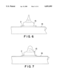
- FIG. 6 is a side view of a protruding bump formed by the wire bonding method in embodiment 2 of the invention.
- FIG. 7 is a side view of a two-stage protruding bump formed by the wiring bonding method in embodiment 2 of the invention.
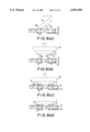
- FIG. 8(a)-8(d) is a diagram showing mounting steps sequentially in embodiment 2 of the invention.
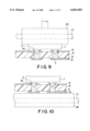
- FIG. 9 is a diagram showing mounting steps sequentially in embodiment 3 of the invention.
- FIG. 10 is a diagram showing mounting steps sequentially in embodiment 4 of the invention.
- FIG. 11 is a diagram showing mounting steps sequentially in embodiment 5 of the invention.
- FIG. 12 is a diagram showing mounting steps sequentially in embodiment 6 of the invention.
- FIG. 13 is a junction sectional view of a semiconductor element and a circuit board after mounting in embodiment 6 of the invention.
- FIG. 14(a)-14(d) is a diagram showing mounting steps sequentially in embodiment 7 of the invention.
- FIG. 15(a)-15(b) is a diagram showing mounting steps sequentially in embodiment 8 of the invention.
- FIG. 16 is a junction sectional view of a semiconductor element and a circuit board after mounting in a conventional mounting method of semiconductor element.
- FIG. 17 is a junction sectional view of a semiconductor element and a circuit board after mounting in a conventional mounting method of semiconductor element.
- FIG. 18 is a junction sectional view of a semiconductor element and a circuit board after mounting in a conventional mounting method of semiconductor element.
- FIG. 19(a)-19(d) is a diagram showing conventional mounting steps sequentially.
- FIG. 20 is a diagram for explaining a problem of a conventional mounting method.
- FIG. 21 is a diagram for explaining a problem of a conventional mounting method.
- the invention as set forth in the claims is a mounting method of semiconductor element comprising a step of forming a hole in a position of a circuit board for connecting a circuit of the circuit board and an electrode of a semiconductor element, a step of filling the hole with a conductive paste for forming an external electrode terminal, a step of forming a protruding bump on the electrode of the semiconductor element, a step of positioning the external electrode terminal and the protruding bump formed on the electrode of the semiconductor element, and a step of pressing the semiconductor element to contact between the conductive paste in the hole and the protruding bump, thereby electrically connecting the electrode of the semiconductor element and the external electrode terminal of the circuit board.
- the protruding bump contacts with the conductive paste in the hole of the circuit board, and is electrically connected, and hence open state or short circuit does not occur.
- the invention as set forth in the claims relates to a mounting method of semiconductor element of the claims, in which the protruding bump formed on the electrode of the semiconductor element is a metal ball bump formed by wire bonding method.
- the protruding bump is formed by electric plating method
- the height of the formed bump is about 25 microns at maximum
- the wire bonding method can form the bump as high as 50 microns or more, so that the amount of the bump filled with the conductive paste in the hole in the circuit board increases, and mounting of higher reliability is realized.
- the invention as set forth in the claims relates to a mounting method of semiconductor element of the claims, which further comprises a step of, after pressing the semiconductor element to contact between the conductive paste charged in the hole of the circuit board and the protruding bump on the electrode of the semiconductor element, heating at least one of the semiconductor element and the circuit board by a heating tool, thereby curing the conductive paste.
- a heating tool By curing the conductive paste, fixing of the semiconductor element and circuit board is stronger, and the junction is higher in reliability.
- it can be done simultaneously with joining in the same equipment in the method of the invention, so that the cycle time of production line of semiconductor element can be shortened.
- the invention as set forth in the claims relates to a mounting method of semiconductor element of any one of the claims, which further comprises a step of, after connecting the electrode of the semiconductor element and the external electrode terminal of the circuit board, pouring an epoxy resin into the space between the semiconductor element and the circuit board, and sealing. Since the active surface of the semiconductor element and the electrode surface are protected by the epoxy resin, the reliability of connection is further increased.
- the invention as set forth in the claims is a mounting method of semiconductor element comprising a step of forming a hole in a position of a circuit board for connecting a circuit of the circuit board and an electrode of a semiconductor element, a step of filling the hole with a conductive paste for forming an external electrode terminal, a step of forming a protruding bump on the electrode of the semiconductor element, a step of disposing an adhesive sheet having a thermosetting resin, a thermoplastic resin, or a mixed thermosetting and thermoplastic resin, on the circuit board forming the external electrode terminal or the protruding bump of the semiconductor element, a step of positioning the external electrode terminal and the protruding bump formed on the electrode of the semiconductor element, a step of pressing the semiconductor element to break through the adhesive sheet by the protruding bump so as to contact between the conductive paste in the hole and the protruding bump, thereby electrically connecting the electrode of the semiconductor element and the external electrode terminal of the circuit board, and a step of heating the semiconductor element by a heating tool to
- the adhesive sheet protects the active surface of the semiconductor element and the electrode surface after melting and curing, the reliability of connection is increased. Further, in the case of using the adhesive sheet, the time required for pressurizing and curing is about 30 seconds, whereas the curing time is about 4 hours in the conventional method by using the epoxy resin, and therefore since the curing time in this method is very short, the cycle time of production line of semiconductor element is shortened.
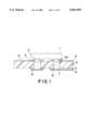
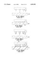
- FIG. 1 is a sectional view of a circuit board mounting a semiconductor element in embodiment 1 of the invention.
- a protruding bump 3 formed on an electrode 2 of a semiconductor element 1 contacts, as being buried in, with a conductive paste 7 filling up a hole 8 of a circuit board 4, so that an external electrode terminal 6 of the circuit board 4 and the electrode 2 of the semiconductor element 1 are electrically connected.
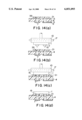
- a process diagram in FIG. 2 a mounting method of semiconductor element of the invention is described below.
- the external electrode terminal 6 of the circuit board 4 and the electrode 2 of the semiconductor element 1 are connected.
- the hole 8 is formed in a position of the circuit board 4, and the conductive paste 7 is printed in to fill up the hole 8 of the circuit board 4 by moving a squeegee 9 as shown in FIG. 2(a), and thus an external electrode terminal 33 of the circuit board 4 is formed.
- the semiconductor element 1 is attracted to a suction nozzle 10, and the protruding bump 3, and the external electrode terminal 33 of the circuit board 4 formed by the conductive paste 7 filling up the hole 8 are positioned.
- the protruding bump 3 of the semiconductor element 1 contacts with the conductive paste 7 in the hole of the circuit board 4, and they are electrically connected.
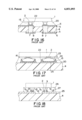
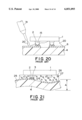
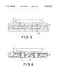
- the circuit board 4 may be also a multi-layer substrate conducting between layers in the substrate by inner via holes as shown in FIG. 3, or the circuit board 4 may be also a multi-layer substrate conducting between layers by through holes as shown in FIG. 4.
- the protruding bump 3 formed on the electrode 2 of the semiconductor element 1 is buried in the conductive paste 7 in the hole 8 of the circuit board 4, and contacts to be connected electrically, short circuit is not formed, and the tolerable range for warping and curving of the circuit board 4 is extended, and open state does not occur, so that the semiconductor element 1 and the circuit board 4 may be joined at high reliability.
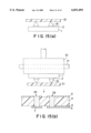
- FIG. 5 is a process diagram showing a forming method of a protruding bump on an electrode of a semiconductor element by employing a wire bonding method according to embodiment 2 of the invention, and the wire bonding method is described below while referring to FIG. 5.
- a metal wire 11 made of gold, copper, aluminum, solder or the like is passed through a capillary 13 made of ceramic or ruby, and a metal ball 12 is formed by electric discharge between the end of the passed metal wire 11 and an electrode 14 called torch.
- the metal ball 12 is pressed on an electrode 2 of a preheated semiconductor element 1, and ultrasonic vibrations are applied.
- the metal ball 12 is joined to the electrode 2.
- the semiconductor element 1 and the circuit board 4 are joined in the method shown in FIG. 8.
- the mounting method in FIG. 8 is same as the method explained in embodiment 1, and its explanation is omitted.
- a high bump of 50 microns or more can be formed by the wire bonding method of the embodiment, as compared with the maximum height of about 25 microns of the protruding bump formed by the conventional electric plating method, and therefore, as shown in FIG. 8(c) and 8(d), the amount of the bump 15 buried in the conductive paste 7 in the hole 8 of the circuit board 4 is increased, and the tolerable range for warping and curving of the circuit board 4 is extended, so that mounting of higher reliability is realized.
- a mounting method of semiconductor element in embodiment 3 of the invention is described below while referring to FIG. 9.
- a semiconductor element 1 is attracted to a suction nozzle 10, and is positioned to an external electrode terminal of a circuit board 4 forming a protruding bump 15 by conductive paste 7 filling up a hole 8, and they are pressed, and the protruding bump 15 is buried in the conductive paste 7.
- the suction nozzle 10 is heated by an incorporated heater 17, and the conductive paste 7 is cured simultaneously with pressing.
- a mounting method of semiconductor element in embodiment 4 of the invention is described below while referring to FIG. 10.
- a semiconductor element 1 is attracted to a suction nozzle 10, and is positioned to an external electrode terminal 33 of a circuit board 4 forming a protruding bump 15 by conductive paste 7 filling up a hole 8, and they are pressed, and the protruding bump 15 is buried in the conductive paste 7.
- a stage 18 holding the circuit board 4 is heated by an incorporated heater 17, and by heating when pressing the semiconductor element 1, the conductive paste 7 is cured with pressing.
- a mounting method of semiconductor element in embodiment 5 of the invention is described below while referring to FIG. 11.
- a semiconductor element 1 is pressed, and a conductive paste 7 in a hole 8 of a circuit board 4 is brought into contact with a protruding bump 15 on an electrode 2 of the semiconductor element 1, a module (circuit board 4 and semiconductor element 1) is put on a conveyor 32,and the entire module is heated by a heater 19 while moving, so that the conductive paste 7 is cured.
- a mounting method of semiconductor element in embodiment 6 of the invention is described below while referring to FIG. 12.
- a mounting method of semiconductor element in embodiment 7 of the invention is described below while referring to FIG. 14.
- a hole 8 in a circuit board 4 is filled with a conductive paste 7 to form an external electrode terminal 33, and an adhesive sheet 21 having a thermosetting resin, a thermoplastic resin, or a mixed thermosetting and thermoplastic resin is disposed on the circuit board 4.
- a semiconductor element 1 is attracted to a suction nozzle 10, and is positioned to an external electrode terminal 33 of the circuit board 4 forming a protruding bump 15 by the conductive paste 7 filling up the hole 8.
- the adhesive sheet 21 is melted and cured, and the active surface of the semiconductor element 1 and the surface of the electrode 2 are protected, so that the reliability of connection is further increased.
- the time required for pressing and curing is about 30 seconds, whereas the curing time of epoxy resin in the prior art is about 4 hours, and therefore the curing time in the embodiment is very short, and the cycle time of production line of semiconductor element 1 can be shortened.
- a mounting method of semiconductor element in embodiment 8 of the invention is described below while referring to FIG. 15.
- an adhesive sheet 21 having a thermosetting resin, a thermoplastic resin, or a mixed thermosetting and thermoplastic resin is disposed preliminarily on the protruding bump 15. It is also possible to disperse particles of nickel, solder, carbon, or gold plated plastic uniformly on the adhesive sheet 21.
- the semiconductor element 1 is attracted to a suction nozzle 10, and is positioned to an external electrode terminal 33 of a circuit board 4 forming the protruding bump 15 by a conductive paste 7 filling up a hole 8, and by pressing, the adhesive sheet 21 is torn off by the protruding bump 15, and the protruding bump 15 is buried in the conductive paste 7.
- the suction nozzle 10 is heated by an incorporated heater 17, and the adhesive sheet 21 is melted and cured simultaneously with pressing.
- the adhesive sheet 21 is melted and cured, and the active surface of the semiconductor element 1 and the surface of the electrode 2 are protected, so that the reliability of connection is further increased.
- the time required for pressing and curing is about 30 seconds, whereas the curing time of epoxy resin in the prior art is about 4 hours, and therefore the curing time in the embodiment is very short, and the cycle time of production line of semiconductor element 1 can be shortened.
- the invention by bringing the protruding bump formed on the electrode of the semiconductor element into contact with the conductive paste in the hole in the circuit board, and connecting the electrode of the semiconductor element and the external electrode terminal of the circuit board electrically, a short circuit between electrodes can be avoided, and the tolerable range for warping and curving of the circuit board is wide, so that an open state between the electrodes can be avoided, and mounting of high electrical reliability is realized.
- the adhesive sheet by preliminarily disposing the adhesive sheet on the circuit board or the protruding bump of the semiconductor element, tearing off the adhesive sheet at the time of mounting so that the protruding bump may contact with the conductive paste in the circuit board hole to connect electrically, and melting and curing the adhesive sheet, the active surface of the semiconductor element and the surface of the electrode can be protected by the adhesive sheet, and therefore the reliability of the connection is increased.
- the time required for pressing and curing is about 30 seconds
- the curing time of epoxy resin in the prior art is about 4 hours, and therefore the curing time in the embodiment is very short, and the time for the sealing process is notably saved, so that the cycle time of production line of semiconductor element can be shortened.
Landscapes
- Engineering & Computer Science (AREA)
- Microelectronics & Electronic Packaging (AREA)
- Manufacturing & Machinery (AREA)
- Wire Bonding (AREA)
- Encapsulation Of And Coatings For Semiconductor Or Solid State Devices (AREA)
Applications Claiming Priority (3)
| Application Number | Priority Date | Filing Date | Title |
|---|---|---|---|
| JP14524196A JP3610999B2 (ja) | 1996-06-07 | 1996-06-07 | 半導体素子の実装方法 |
| JP8-145241 | 1996-06-07 | ||
| PCT/JP1997/001971 WO1997047031A1 (en) | 1996-06-07 | 1997-06-06 | Method for mounting semiconductor chip |
Related Child Applications (1)
| Application Number | Title | Priority Date | Filing Date |
|---|---|---|---|
| US09/528,116 Continuation US6531022B1 (en) | 1996-06-07 | 2000-03-17 | Mounting method of semiconductor element |
Publications (1)
| Publication Number | Publication Date |
|---|---|
| US6051093A true US6051093A (en) | 2000-04-18 |
Family
ID=15380594
Family Applications (2)
| Application Number | Title | Priority Date | Filing Date |
|---|---|---|---|
| US09/011,603 Expired - Fee Related US6051093A (en) | 1996-06-07 | 1997-06-06 | Mounting method of semiconductor element |
| US09/528,116 Expired - Fee Related US6531022B1 (en) | 1996-06-07 | 2000-03-17 | Mounting method of semiconductor element |
Family Applications After (1)
| Application Number | Title | Priority Date | Filing Date |
|---|---|---|---|
| US09/528,116 Expired - Fee Related US6531022B1 (en) | 1996-06-07 | 2000-03-17 | Mounting method of semiconductor element |
Country Status (6)
| Country | Link |
|---|---|
| US (2) | US6051093A (de) |
| EP (1) | EP0844657A4 (de) |
| JP (1) | JP3610999B2 (de) |
| KR (1) | KR100457609B1 (de) |
| CN (1) | CN1110078C (de) |
| WO (1) | WO1997047031A1 (de) |
Cited By (31)
| Publication number | Priority date | Publication date | Assignee | Title |
|---|---|---|---|---|
| US6193136B1 (en) * | 1998-08-20 | 2001-02-27 | Matsushita Electric Industrial Co., Ltd. | Component mounting method and apparatus |
| US6297141B1 (en) * | 1997-03-03 | 2001-10-02 | Nec Corporation | Mounting assembly of integrated circuit device and method for production thereof |
| US20020060904A1 (en) * | 2000-09-26 | 2002-05-23 | Kazuhito Higuchi | Electronic component, circuit device, method for manufacturing the circuit device, and semiconductor device |
| US20020079594A1 (en) * | 2000-12-26 | 2002-06-27 | Seiko Epson Corporation | Semiconductor device and method of manufacture thereof, circuit board, and electronic instrument |
| US6437669B1 (en) | 2000-09-29 | 2002-08-20 | Applied Micro Circuits Corporation | Microwave to millimeter wave frequency substrate interface |
| US20020127772A1 (en) * | 1998-12-17 | 2002-09-12 | Charles W.C. Lin. | Bumpless flip chip assembly with solder via |
| US20020180029A1 (en) * | 2001-04-25 | 2002-12-05 | Hideki Higashitani | Semiconductor device with intermediate connector |
| US20030035272A1 (en) * | 2001-05-29 | 2003-02-20 | Curcio Brian E. | Solid via layer to layer interconnect |
| US6537400B1 (en) * | 2000-03-06 | 2003-03-25 | Micron Technology, Inc. | Automated method of attaching flip chip devices to a substrate |
| US6538898B1 (en) * | 2000-05-01 | 2003-03-25 | Micron Technology, Inc. | Method and apparatus of die attachment for BOC and F/C surface mount |
| US6541872B1 (en) | 1999-01-11 | 2003-04-01 | Micron Technology, Inc. | Multi-layered adhesive for attaching a semiconductor die to a substrate |
| US6543674B2 (en) * | 2001-02-06 | 2003-04-08 | Fujitsu Limited | Multilayer interconnection and method |
| US20030172525A1 (en) * | 2001-10-16 | 2003-09-18 | International Business Machines Corporation | Interconnect structure and method of making same |
| US20030224555A1 (en) * | 2002-03-22 | 2003-12-04 | Masakuni Shiozawa | Apparatus for manufacturing an electronic device, method of manufacturing an electronic device, and program for manufacturing an electronic device |
| US20040078963A1 (en) * | 2000-08-03 | 2004-04-29 | Tessera, Inc. | Method of making a microelectronic package including a component having conductive elements on a top side and a bottom side thereof |
| US20040091687A1 (en) * | 2001-06-13 | 2004-05-13 | Koji Kondo | Method for manufacturing printed wiring board with embedded electric device |
| US6818461B2 (en) * | 1999-01-14 | 2004-11-16 | Matsushita Electric Industrial Co., Ltd. | Method of producing mounting structure and mounting structure produced by the same |
| US20040238603A1 (en) * | 2003-05-27 | 2004-12-02 | Seiko Epson Corporation | Method of mounting electronic component, structure for mounting electronic component, electronic component module, and electronic apparatus |
| US20050104180A1 (en) * | 2003-11-14 | 2005-05-19 | Vassoudevane Lebonheur | Electronic device with reduced entrapment of material between die and substrate electrical connections |
| US20060044771A1 (en) * | 2004-08-24 | 2006-03-02 | Yeo Chee K | Electronic module with conductive polymer |
| US20070184604A1 (en) * | 1999-10-05 | 2007-08-09 | Nec Electronics Corporation | Multilayer interconnection board, semiconductor device having the same, and method of forming the same as well as method of mounting the semicondutor chip on the interconnection board |
| CN100437961C (zh) * | 2003-10-07 | 2008-11-26 | 松下电器产业株式会社 | 半导体元件的安装方法及半导体元件安装基板 |
| US20120067412A1 (en) * | 2010-09-16 | 2012-03-22 | Weibezahn Karl S | Solder bonding entities to solid material |
| US20140291006A1 (en) * | 2013-03-28 | 2014-10-02 | Fujitsu Limited | Printed circuit board solder mounting method and solder mount structure |
| EP3309829A1 (de) * | 2016-10-14 | 2018-04-18 | Iriso Electronics Co., Ltd. | Leiterplatte und schaltungsvorrichtung |
| US9975194B2 (en) * | 2013-09-17 | 2018-05-22 | Abb Schweiz Ag | Method for ultrasonic welding with particles trapping |
| US20190295982A1 (en) * | 2016-11-29 | 2019-09-26 | Shenzhen Xiuyuan Electronic Technology Co., Ltd | Chip Wiring Method and Structure |
| US20190326261A1 (en) * | 2016-11-30 | 2019-10-24 | Shenzhen Xiuyuan Electronic Technology Co., Ltd | Integrated Circuit Multichip Stacked Packaging Structure and Method |
| US11056808B2 (en) | 2016-08-26 | 2021-07-06 | Murata Manufacturing Co., Ltd. | Resin multilayer substrate, transmission line, module, and method of manufacturing module |
| US11088063B2 (en) * | 2018-08-22 | 2021-08-10 | Liquid Wire Inc. | Structures with deformable conductors |
| CN114496964A (zh) * | 2022-01-27 | 2022-05-13 | 锐芯微电子股份有限公司 | 芯片引脚焊盘的引出连接结构及方法 |
Families Citing this family (62)
| Publication number | Priority date | Publication date | Assignee | Title |
|---|---|---|---|---|
| US5064520A (en) | 1989-02-15 | 1991-11-12 | Hitachi, Ltd. | Method and apparatus for forming a film |
| JP3539315B2 (ja) * | 1999-06-22 | 2004-07-07 | 株式会社村田製作所 | 電子デバイス素子の実装方法、および弾性表面波装置の製造方法 |
| JP2001257453A (ja) * | 2000-03-09 | 2001-09-21 | Shinko Electric Ind Co Ltd | 配線基板、半導体装置及びそれらの製造方法 |
| JP2001339011A (ja) * | 2000-03-24 | 2001-12-07 | Shinko Electric Ind Co Ltd | 半導体装置およびその製造方法 |
| JP4759791B2 (ja) * | 2000-07-27 | 2011-08-31 | 日亜化学工業株式会社 | 光半導体素子とその製造方法 |
| KR20020046754A (ko) * | 2000-12-15 | 2002-06-21 | 밍 루 | 표면실장용 인쇄회로 기판과 부품 실장 방법 |
| JP2002313840A (ja) * | 2001-04-17 | 2002-10-25 | Matsushita Electric Ind Co Ltd | 半導体素子実装基板及びその製造方法 |
| JP4051893B2 (ja) * | 2001-04-18 | 2008-02-27 | 株式会社日立製作所 | 電子機器 |
| DE10126655A1 (de) * | 2001-06-01 | 2002-12-05 | Endress & Hauser Gmbh & Co Kg | Leiterplatte mit mindestens einem elektronischen Bauteil |
| CN101370360B (zh) * | 2001-06-13 | 2011-04-27 | 株式会社电装 | 埋有电子器件的印刷线路板及其制造方法 |
| JP3615727B2 (ja) * | 2001-10-31 | 2005-02-02 | 新光電気工業株式会社 | 半導体装置用パッケージ |
| US20030150645A1 (en) * | 2002-02-12 | 2003-08-14 | Chia-Pin Chiu | Method and apparatus for coupling a microelectronic device package to a circuit board |
| US7754976B2 (en) * | 2002-04-15 | 2010-07-13 | Hamilton Sundstrand Corporation | Compact circuit carrier package |
| KR100873041B1 (ko) * | 2002-06-12 | 2008-12-09 | 삼성테크윈 주식회사 | 반도체 팩키지의 범프와 동박 회로 패턴 사이의 접속 방법및,그를 위한 반도체 팩키지의 범프 구조 |
| US6964881B2 (en) * | 2002-08-27 | 2005-11-15 | Micron Technology, Inc. | Multi-chip wafer level system packages and methods of forming same |
| JP4056424B2 (ja) * | 2003-05-16 | 2008-03-05 | シャープ株式会社 | 半導体装置の製造方法 |
| US7408258B2 (en) * | 2003-08-20 | 2008-08-05 | Salmon Technologies, Llc | Interconnection circuit and electronic module utilizing same |
| US7135397B2 (en) * | 2003-09-10 | 2006-11-14 | Texas Instruments Incorporated | Method and system for packaging ball grid arrays |
| US20050184376A1 (en) * | 2004-02-19 | 2005-08-25 | Salmon Peter C. | System in package |
| US7331503B2 (en) * | 2004-10-29 | 2008-02-19 | Intel Corporation | Solder printing process to reduce void formation in a microvia |
| US7427809B2 (en) * | 2004-12-16 | 2008-09-23 | Salmon Technologies, Llc | Repairable three-dimensional semiconductor subsystem |
| US20070007983A1 (en) * | 2005-01-06 | 2007-01-11 | Salmon Peter C | Semiconductor wafer tester |
| JP4291279B2 (ja) * | 2005-01-26 | 2009-07-08 | パナソニック株式会社 | 可撓性多層回路基板 |
| US7851348B2 (en) * | 2005-06-14 | 2010-12-14 | Abhay Misra | Routingless chip architecture |
| US20060281303A1 (en) * | 2005-06-14 | 2006-12-14 | John Trezza | Tack & fuse chip bonding |
| US7838997B2 (en) * | 2005-06-14 | 2010-11-23 | John Trezza | Remote chip attachment |
| US7560813B2 (en) | 2005-06-14 | 2009-07-14 | John Trezza | Chip-based thermo-stack |
| US7786592B2 (en) | 2005-06-14 | 2010-08-31 | John Trezza | Chip capacitive coupling |
| US7687400B2 (en) * | 2005-06-14 | 2010-03-30 | John Trezza | Side stacking apparatus and method |
| US7215032B2 (en) * | 2005-06-14 | 2007-05-08 | Cubic Wafer, Inc. | Triaxial through-chip connection |
| US7884483B2 (en) | 2005-06-14 | 2011-02-08 | Cufer Asset Ltd. L.L.C. | Chip connector |
| US7781886B2 (en) | 2005-06-14 | 2010-08-24 | John Trezza | Electronic chip contact structure |
| US8456015B2 (en) * | 2005-06-14 | 2013-06-04 | Cufer Asset Ltd. L.L.C. | Triaxial through-chip connection |
| US7586747B2 (en) * | 2005-08-01 | 2009-09-08 | Salmon Technologies, Llc. | Scalable subsystem architecture having integrated cooling channels |
| US20070023923A1 (en) * | 2005-08-01 | 2007-02-01 | Salmon Peter C | Flip chip interface including a mixed array of heat bumps and signal bumps |
| US20070023904A1 (en) * | 2005-08-01 | 2007-02-01 | Salmon Peter C | Electro-optic interconnection apparatus and method |
| US20070023889A1 (en) * | 2005-08-01 | 2007-02-01 | Salmon Peter C | Copper substrate with feedthroughs and interconnection circuits |
| FR2894070B1 (fr) * | 2005-11-30 | 2008-04-11 | 3D Plus Sa Sa | Module electronique 3d |
| CN100438008C (zh) * | 2006-03-01 | 2008-11-26 | 南茂科技股份有限公司 | 高频集成电路封装构造及其制造方法 |
| WO2007125791A1 (ja) * | 2006-04-24 | 2007-11-08 | Alps Electric Co., Ltd. | 配線基板の製造方法 |
| US20070281460A1 (en) * | 2006-06-06 | 2007-12-06 | Cubic Wafer, Inc. | Front-end processed wafer having through-chip connections |
| US7687397B2 (en) * | 2006-06-06 | 2010-03-30 | John Trezza | Front-end processed wafer having through-chip connections |
| CN101447443B (zh) * | 2006-08-15 | 2010-06-02 | 南茂科技股份有限公司 | 高频集成电路封装构造的制造方法 |
| CN100499097C (zh) * | 2006-08-21 | 2009-06-10 | 南茂科技股份有限公司 | 增进嵌埋凸块接合性的高频集成电路封装构造及制造方法 |
| WO2008032755A1 (en) * | 2006-09-11 | 2008-03-20 | Panasonic Corporation | Electronic component placing apparatus and electronic component mounting method |
| CN101529585B (zh) * | 2006-10-20 | 2012-07-04 | 日本电气株式会社 | 电子设备的封装结构及封装制造方法 |
| US7670874B2 (en) | 2007-02-16 | 2010-03-02 | John Trezza | Plated pillar package formation |
| US20080206516A1 (en) * | 2007-02-22 | 2008-08-28 | Yoshihiko Matsushima | Surface mount circuit board, method for manufacturing surface mount circuit board, and method for mounting surface mount electronic devices |
| JP5183708B2 (ja) * | 2010-09-21 | 2013-04-17 | 株式会社日立製作所 | 半導体装置およびその製造方法 |
| EP2463809A1 (de) * | 2010-12-07 | 2012-06-13 | NagraID S.A. | Elektronische Karte mit elektrischem Kontakt, die eine elektronische Einheit und/oder eine Antenne umfasst |
| EP2656699A1 (de) * | 2010-12-21 | 2013-10-30 | Linxens Holding | Verfahren zur herstellung einer oberflächenmontierten vorrichtung und entsprechende oberflächenmontierte vorrichtung |
| JP5533914B2 (ja) * | 2011-08-31 | 2014-06-25 | 株式会社デンソー | 多層基板 |
| KR101388739B1 (ko) * | 2012-04-27 | 2014-04-25 | 삼성전기주식회사 | 반도체 패키지 |
| TWI509756B (zh) * | 2013-09-30 | 2015-11-21 | Chipmos Technologies Inc | 薄膜覆晶封裝結構 |
| CN103682043A (zh) * | 2013-11-28 | 2014-03-26 | 天津金玛光电有限公司 | 一种水平式led芯片的固晶方法及采用该方法制备的led光源 |
| JP6278817B2 (ja) | 2014-04-24 | 2018-02-14 | Jfeケミカル株式会社 | ポリアミド酸組成物およびポリイミド組成物 |
| DE202014010576U1 (de) * | 2014-06-12 | 2016-01-07 | Pfisterer Kontaktsysteme Gmbh | Vorrichtung zum Kontaktieren eines elektrischen Leiters sowie Anschluss- oder Verbindungseinrichtung mit einer solchen Vorrichtung |
| CN106816417B (zh) * | 2017-01-13 | 2019-02-12 | 南京大学 | 一种高密度封装及其制造方法 |
| KR102432216B1 (ko) * | 2017-07-11 | 2022-08-12 | 쑤저우 레킨 세미컨덕터 컴퍼니 리미티드 | 발광소자 패키지 |
| CN107949166B (zh) * | 2017-11-30 | 2020-04-14 | 广州兴森快捷电路科技有限公司 | 埋置元件电路板的制作方法及埋置元件电路板 |
| CN111083879B (zh) * | 2019-07-26 | 2021-02-02 | 微智医疗器械有限公司 | 电子元件与电路板的连接方法、电路板组件及电子设备 |
| CN111540722B (zh) * | 2020-07-07 | 2021-05-14 | 甬矽电子(宁波)股份有限公司 | 芯片封装结构及封装方法 |
Citations (14)
| Publication number | Priority date | Publication date | Assignee | Title |
|---|---|---|---|---|
| JPS60126856A (ja) * | 1983-12-13 | 1985-07-06 | Sanyo Electric Co Ltd | 半導体装置の組立方法 |
| JPH01198040A (ja) * | 1988-02-03 | 1989-08-09 | Omron Tateisi Electron Co | 半導体素子の実装法 |
| US5014111A (en) * | 1987-12-08 | 1991-05-07 | Matsushita Electric Industrial Co., Ltd. | Electrical contact bump and a package provided with the same |
| EP0482940A1 (de) * | 1990-10-24 | 1992-04-29 | Nec Corporation | Verfahren zur Herstellung einer elektrischen Verbindung für eine integrierte Schaltung |
| JPH04267394A (ja) * | 1991-02-22 | 1992-09-22 | Tatsuta Electric Wire & Cable Co Ltd | フレキシブルプリント板 |
| JPH05267394A (ja) * | 1992-03-19 | 1993-10-15 | Sumitomo Electric Ind Ltd | 半導体素子の実装方法 |
| US5274916A (en) * | 1991-12-18 | 1994-01-04 | Murata Manufacturing Co., Ltd. | Method of manufacturing ceramic multilayer electronic component |
| JPH0669278A (ja) * | 1992-08-18 | 1994-03-11 | Toshiba Corp | 半導体素子の接続方法 |
| US5384952A (en) * | 1990-12-26 | 1995-01-31 | Nec Corporation | Method of connecting an integrated circuit chip to a substrate |
| US5407864A (en) * | 1992-07-24 | 1995-04-18 | Samsung Electronics Co., Ltd. | Process for mounting a semiconductor chip and depositing contacts into through holes of a circuit board and of an insulating interposer and onto the chip |
| EP0735579A1 (de) * | 1995-03-27 | 1996-10-02 | Motorola, Inc. | Struktur und Verfahren zum Verbinden von Substraten |
| US5615477A (en) * | 1994-09-06 | 1997-04-01 | Sheldahl, Inc. | Method for interconnecting a flip chip to a printed circuit substrate |
| US5843251A (en) * | 1989-03-09 | 1998-12-01 | Hitachi Chemical Co., Ltd. | Process for connecting circuits and adhesive film used therefor |
| US5848466A (en) * | 1996-11-19 | 1998-12-15 | Motorola, Inc. | Method for forming a microelectronic assembly |
Family Cites Families (4)
| Publication number | Priority date | Publication date | Assignee | Title |
|---|---|---|---|---|
| JPS5267394A (en) * | 1975-03-31 | 1977-06-03 | Hitachi Ltd | Eluate programing device |
| JPH039278A (ja) * | 1989-06-07 | 1991-01-17 | Toshiba Corp | 故障点標定装置用サージ受信装置 |
| JP2786734B2 (ja) * | 1990-09-28 | 1998-08-13 | 株式会社東芝 | 半導体装置 |
| JPH1198040A (ja) * | 1997-09-19 | 1999-04-09 | Fujitsu General Ltd | 発電機能付衛星受信アンテナ |
-
1996
- 1996-06-07 JP JP14524196A patent/JP3610999B2/ja not_active Expired - Fee Related
-
1997
- 1997-06-06 US US09/011,603 patent/US6051093A/en not_active Expired - Fee Related
- 1997-06-06 KR KR10-1998-0700903A patent/KR100457609B1/ko not_active Expired - Fee Related
- 1997-06-06 CN CN97190666A patent/CN1110078C/zh not_active Expired - Fee Related
- 1997-06-06 WO PCT/JP1997/001971 patent/WO1997047031A1/ja not_active Ceased
- 1997-06-06 EP EP97925302A patent/EP0844657A4/de not_active Withdrawn
-
2000
- 2000-03-17 US US09/528,116 patent/US6531022B1/en not_active Expired - Fee Related
Patent Citations (14)
| Publication number | Priority date | Publication date | Assignee | Title |
|---|---|---|---|---|
| JPS60126856A (ja) * | 1983-12-13 | 1985-07-06 | Sanyo Electric Co Ltd | 半導体装置の組立方法 |
| US5014111A (en) * | 1987-12-08 | 1991-05-07 | Matsushita Electric Industrial Co., Ltd. | Electrical contact bump and a package provided with the same |
| JPH01198040A (ja) * | 1988-02-03 | 1989-08-09 | Omron Tateisi Electron Co | 半導体素子の実装法 |
| US5843251A (en) * | 1989-03-09 | 1998-12-01 | Hitachi Chemical Co., Ltd. | Process for connecting circuits and adhesive film used therefor |
| EP0482940A1 (de) * | 1990-10-24 | 1992-04-29 | Nec Corporation | Verfahren zur Herstellung einer elektrischen Verbindung für eine integrierte Schaltung |
| US5384952A (en) * | 1990-12-26 | 1995-01-31 | Nec Corporation | Method of connecting an integrated circuit chip to a substrate |
| JPH04267394A (ja) * | 1991-02-22 | 1992-09-22 | Tatsuta Electric Wire & Cable Co Ltd | フレキシブルプリント板 |
| US5274916A (en) * | 1991-12-18 | 1994-01-04 | Murata Manufacturing Co., Ltd. | Method of manufacturing ceramic multilayer electronic component |
| JPH05267394A (ja) * | 1992-03-19 | 1993-10-15 | Sumitomo Electric Ind Ltd | 半導体素子の実装方法 |
| US5407864A (en) * | 1992-07-24 | 1995-04-18 | Samsung Electronics Co., Ltd. | Process for mounting a semiconductor chip and depositing contacts into through holes of a circuit board and of an insulating interposer and onto the chip |
| JPH0669278A (ja) * | 1992-08-18 | 1994-03-11 | Toshiba Corp | 半導体素子の接続方法 |
| US5615477A (en) * | 1994-09-06 | 1997-04-01 | Sheldahl, Inc. | Method for interconnecting a flip chip to a printed circuit substrate |
| EP0735579A1 (de) * | 1995-03-27 | 1996-10-02 | Motorola, Inc. | Struktur und Verfahren zum Verbinden von Substraten |
| US5848466A (en) * | 1996-11-19 | 1998-12-15 | Motorola, Inc. | Method for forming a microelectronic assembly |
Non-Patent Citations (5)
| Title |
|---|
| English translation of Form PCT/IS/210. * |
| European Search Report for Int l Appln No. 97925302.8 dated Feb. 26, 1999. * |
| European Search Report for Int'l Appln No. 97925302.8 dated Feb. 26, 1999. |
| Japanese language search report for Int l Appln. No. PCT/JP97/01971 dated Dec. 8, 1997. * |
| Japanese language search report for Int'l Appln. No. PCT/JP97/01971 dated Dec. 8, 1997. |
Cited By (59)
| Publication number | Priority date | Publication date | Assignee | Title |
|---|---|---|---|---|
| US6297141B1 (en) * | 1997-03-03 | 2001-10-02 | Nec Corporation | Mounting assembly of integrated circuit device and method for production thereof |
| US6193136B1 (en) * | 1998-08-20 | 2001-02-27 | Matsushita Electric Industrial Co., Ltd. | Component mounting method and apparatus |
| US6467670B2 (en) | 1998-08-20 | 2002-10-22 | Matsushita Electric Industrial Co., Ltd. | Method and apparatus for mounting component |
| US20020127772A1 (en) * | 1998-12-17 | 2002-09-12 | Charles W.C. Lin. | Bumpless flip chip assembly with solder via |
| US6541872B1 (en) | 1999-01-11 | 2003-04-01 | Micron Technology, Inc. | Multi-layered adhesive for attaching a semiconductor die to a substrate |
| US6770164B1 (en) * | 1999-01-11 | 2004-08-03 | Micron Technology, Inc. | Method for attaching a semiconductor die to a substrate |
| US6818461B2 (en) * | 1999-01-14 | 2004-11-16 | Matsushita Electric Industrial Co., Ltd. | Method of producing mounting structure and mounting structure produced by the same |
| US20070184604A1 (en) * | 1999-10-05 | 2007-08-09 | Nec Electronics Corporation | Multilayer interconnection board, semiconductor device having the same, and method of forming the same as well as method of mounting the semicondutor chip on the interconnection board |
| US8008130B2 (en) * | 1999-10-05 | 2011-08-30 | Renesas Electronics Corporation | Multilayer interconnection board, semiconductor device having the same, and method of forming the same as well as method of mounting the semicondutor chip on the interconnection board |
| US6793749B2 (en) | 2000-03-06 | 2004-09-21 | Micron Technology, Inc. | Automated method of attaching flip-chip devices to a substrate |
| US6537400B1 (en) * | 2000-03-06 | 2003-03-25 | Micron Technology, Inc. | Automated method of attaching flip chip devices to a substrate |
| US6773523B2 (en) | 2000-03-06 | 2004-08-10 | Micron Technology, Inc. | Automated method of attaching flip chip devices to a substrate |
| US6538898B1 (en) * | 2000-05-01 | 2003-03-25 | Micron Technology, Inc. | Method and apparatus of die attachment for BOC and F/C surface mount |
| US6691406B2 (en) | 2000-05-01 | 2004-02-17 | Micron Technology, Inc. | Methods of die attachment for BOC and F/C surface mount |
| US20040078963A1 (en) * | 2000-08-03 | 2004-04-29 | Tessera, Inc. | Method of making a microelectronic package including a component having conductive elements on a top side and a bottom side thereof |
| US7188413B2 (en) * | 2000-08-03 | 2007-03-13 | Tessera, Inc. | Method of making a microelectronic package |
| US20020060904A1 (en) * | 2000-09-26 | 2002-05-23 | Kazuhito Higuchi | Electronic component, circuit device, method for manufacturing the circuit device, and semiconductor device |
| US6862189B2 (en) * | 2000-09-26 | 2005-03-01 | Kabushiki Kaisha Toshiba | Electronic component, circuit device, method for manufacturing the circuit device, and semiconductor device |
| US6437669B1 (en) | 2000-09-29 | 2002-08-20 | Applied Micro Circuits Corporation | Microwave to millimeter wave frequency substrate interface |
| US20020079594A1 (en) * | 2000-12-26 | 2002-06-27 | Seiko Epson Corporation | Semiconductor device and method of manufacture thereof, circuit board, and electronic instrument |
| US6846699B2 (en) * | 2000-12-26 | 2005-01-25 | Seiko Epson Corporation | Semiconductor device and method of manufacture thereof, circuit board, and electronic instrument |
| US6543674B2 (en) * | 2001-02-06 | 2003-04-08 | Fujitsu Limited | Multilayer interconnection and method |
| US20020180029A1 (en) * | 2001-04-25 | 2002-12-05 | Hideki Higashitani | Semiconductor device with intermediate connector |
| US7247508B2 (en) | 2001-04-25 | 2007-07-24 | Matsushita Electric Industrial Co., Ltd. | Semiconductor device with intermediate connector |
| US20050142693A1 (en) * | 2001-04-25 | 2005-06-30 | Hideki Higashitani | Semiconductor device with intermediate connector |
| US7076869B2 (en) * | 2001-05-29 | 2006-07-18 | International Business Machines Corporation | Solid via layer to layer interconnect |
| US20030035272A1 (en) * | 2001-05-29 | 2003-02-20 | Curcio Brian E. | Solid via layer to layer interconnect |
| US20040091687A1 (en) * | 2001-06-13 | 2004-05-13 | Koji Kondo | Method for manufacturing printed wiring board with embedded electric device |
| US7165321B2 (en) | 2001-06-13 | 2007-01-23 | Denso Corporation | Method for manufacturing printed wiring board with embedded electric device |
| US6931726B2 (en) | 2001-10-16 | 2005-08-23 | International Business Machines Corporation | Method of making and interconnect structure |
| US20030172525A1 (en) * | 2001-10-16 | 2003-09-18 | International Business Machines Corporation | Interconnect structure and method of making same |
| US6660945B2 (en) | 2001-10-16 | 2003-12-09 | International Business Machines Corporation | Interconnect structure and method of making same |
| US20030224555A1 (en) * | 2002-03-22 | 2003-12-04 | Masakuni Shiozawa | Apparatus for manufacturing an electronic device, method of manufacturing an electronic device, and program for manufacturing an electronic device |
| US20060096701A1 (en) * | 2002-03-22 | 2006-05-11 | Masakuni Shiozawa | Apparatus for manufacturing an electronic device, method of manufacturing an electronic device, and program for manufacturing an electronic device |
| US7017636B2 (en) * | 2002-03-22 | 2006-03-28 | Seiko Epson Corporation | Apparatus for manufacturing an electronic device, method of manufacturing an electronic device, and program for manufacturing an electronic device |
| US7410826B2 (en) | 2002-03-22 | 2008-08-12 | Seiko Epson Corporation | Apparatus for manufacturing an electronic device, method of manufacturing an electronic device, and program for manufacturing an electronic device |
| US20040238603A1 (en) * | 2003-05-27 | 2004-12-02 | Seiko Epson Corporation | Method of mounting electronic component, structure for mounting electronic component, electronic component module, and electronic apparatus |
| US7278564B2 (en) * | 2003-05-27 | 2007-10-09 | Seiko Epson Corporation | Method of mounting electronic component, structure for mounting electronic component, electronic component module, and electronic apparatus |
| CN100437961C (zh) * | 2003-10-07 | 2008-11-26 | 松下电器产业株式会社 | 半导体元件的安装方法及半导体元件安装基板 |
| US20050104180A1 (en) * | 2003-11-14 | 2005-05-19 | Vassoudevane Lebonheur | Electronic device with reduced entrapment of material between die and substrate electrical connections |
| US20060044771A1 (en) * | 2004-08-24 | 2006-03-02 | Yeo Chee K | Electronic module with conductive polymer |
| US20120067412A1 (en) * | 2010-09-16 | 2012-03-22 | Weibezahn Karl S | Solder bonding entities to solid material |
| US8210424B2 (en) * | 2010-09-16 | 2012-07-03 | Hewlett-Packard Development Company, L.P. | Soldering entities to a monolithic metallic sheet |
| US20140291006A1 (en) * | 2013-03-28 | 2014-10-02 | Fujitsu Limited | Printed circuit board solder mounting method and solder mount structure |
| US9975194B2 (en) * | 2013-09-17 | 2018-05-22 | Abb Schweiz Ag | Method for ultrasonic welding with particles trapping |
| US11056808B2 (en) | 2016-08-26 | 2021-07-06 | Murata Manufacturing Co., Ltd. | Resin multilayer substrate, transmission line, module, and method of manufacturing module |
| EP3309829A1 (de) * | 2016-10-14 | 2018-04-18 | Iriso Electronics Co., Ltd. | Leiterplatte und schaltungsvorrichtung |
| US10624206B2 (en) | 2016-10-14 | 2020-04-14 | Iriso Electronics Co., Ltd. | Circuit board and circuit device |
| US10847496B2 (en) * | 2016-11-29 | 2020-11-24 | Shenzhen Xiuyuan Electronic Technology Co., Ltd | Chip wiring method and structure |
| US20190295982A1 (en) * | 2016-11-29 | 2019-09-26 | Shenzhen Xiuyuan Electronic Technology Co., Ltd | Chip Wiring Method and Structure |
| US20190326207A1 (en) * | 2016-11-30 | 2019-10-24 | Shenzhen Xiuyuan Electronic Technology Co., Ltd. | Integrated Circuit Packaging Method and Integrated Packaged Circuit |
| US20190326261A1 (en) * | 2016-11-30 | 2019-10-24 | Shenzhen Xiuyuan Electronic Technology Co., Ltd | Integrated Circuit Multichip Stacked Packaging Structure and Method |
| US10615151B2 (en) * | 2016-11-30 | 2020-04-07 | Shenzhen Xiuyuan Electronic Technology Co., Ltd | Integrated circuit multichip stacked packaging structure and method |
| US10867959B2 (en) * | 2016-11-30 | 2020-12-15 | Shenzhen Xiuyuan Electronic Technology Co., Ltd | Integrated circuit packaging method and integrated packaged circuit |
| US11088063B2 (en) * | 2018-08-22 | 2021-08-10 | Liquid Wire Inc. | Structures with deformable conductors |
| US11594480B2 (en) | 2018-08-22 | 2023-02-28 | Liquid Wire Inc. | Structures with deformable conductors |
| US11955420B2 (en) | 2018-08-22 | 2024-04-09 | Liquid Wire Inc. | Structures with deformable conductors |
| US12125778B2 (en) | 2018-08-22 | 2024-10-22 | Liquid Wire Inc. | Structures with deformable conductors |
| CN114496964A (zh) * | 2022-01-27 | 2022-05-13 | 锐芯微电子股份有限公司 | 芯片引脚焊盘的引出连接结构及方法 |
Also Published As
| Publication number | Publication date |
|---|---|
| EP0844657A1 (de) | 1998-05-27 |
| KR100457609B1 (ko) | 2005-01-15 |
| JP3610999B2 (ja) | 2005-01-19 |
| WO1997047031A1 (en) | 1997-12-11 |
| US6531022B1 (en) | 2003-03-11 |
| KR19990036235A (ko) | 1999-05-25 |
| EP0844657A4 (de) | 1999-04-14 |
| JPH09326419A (ja) | 1997-12-16 |
| CN1110078C (zh) | 2003-05-28 |
| CN1195422A (zh) | 1998-10-07 |
Similar Documents
| Publication | Publication Date | Title |
|---|---|---|
| US6051093A (en) | Mounting method of semiconductor element | |
| KR100384314B1 (ko) | 회로기판에의 전자부품 실장방법 및 장치 | |
| US6622380B1 (en) | Methods for manufacturing microelectronic devices and methods for mounting microelectronic packages to circuit boards | |
| KR100288035B1 (ko) | 플립칩 접속방법, 플립칩 접속 구조체 및 그것을 사용한 전자기기 | |
| KR100563890B1 (ko) | 전기적 접속 장치 및 전기적 접속 방법 | |
| WO2001086716A1 (en) | Semiconductor device mounting circuit board, method of producing the same, and method of producing mounting structure using the same | |
| KR20020044577A (ko) | 개선된 플립-칩 결합 패키지 | |
| KR100355323B1 (ko) | 캐리어와 그를 포함하는 반도체 장치 | |
| JPH10112476A (ja) | 半導体装置の製造方法 | |
| JP2004363220A (ja) | 実装構造体の製造方法及び接続体 | |
| JP2574369B2 (ja) | 半導体チップの実装体およびその実装方法 | |
| JP2002033349A (ja) | 半導体素子の実装方法、及び回路基板 | |
| JP2001015641A (ja) | 電子部品の接続構造及び接続方法 | |
| JP4024458B2 (ja) | 半導体装置の実装方法および半導体装置実装体の製造方法 | |
| JPH11111755A (ja) | 半導体装置の製造方法 | |
| JP2000091380A (ja) | フリップチップの実装構造 | |
| JP3672702B2 (ja) | 部品実装方法 | |
| JP2002026065A (ja) | 半導体素子の実装方法、及び回路基板 | |
| JP3721986B2 (ja) | 半導体装置及びその製造方法 | |
| JP3174975B2 (ja) | 電子部品搭載装置 | |
| JPH08274209A (ja) | チップキャリヤ及びその製造方法 | |
| JP3934739B2 (ja) | 差込み型電子制御ユニット、および配線基板とプラグ部材との接続構造 | |
| JP2002118350A (ja) | フレキシブルプリント基板へのコネクタ接続方法 | |
| JPH08153751A (ja) | 電子デバイス組立体およびその製造方法 | |
| JPH08213426A (ja) | 集積回路の実装方法 |
Legal Events
| Date | Code | Title | Description |
|---|---|---|---|
| AS | Assignment |
Owner name: MATSUSHITA ELECTRIC INDUSTRIAL CO., LTD., JAPAN Free format text: ASSIGNMENT OF ASSIGNORS INTEREST;ASSIGNOR:TSUKAHARA, NORIHITO;REEL/FRAME:009154/0039 Effective date: 19980129 |
|
| FEPP | Fee payment procedure |
Free format text: PAYOR NUMBER ASSIGNED (ORIGINAL EVENT CODE: ASPN); ENTITY STATUS OF PATENT OWNER: LARGE ENTITY |
|
| CC | Certificate of correction | ||
| FPAY | Fee payment |
Year of fee payment: 4 |
|
| FPAY | Fee payment |
Year of fee payment: 8 |
|
| FEPP | Fee payment procedure |
Free format text: PAYOR NUMBER ASSIGNED (ORIGINAL EVENT CODE: ASPN); ENTITY STATUS OF PATENT OWNER: LARGE ENTITY Free format text: PAYER NUMBER DE-ASSIGNED (ORIGINAL EVENT CODE: RMPN); ENTITY STATUS OF PATENT OWNER: LARGE ENTITY |
|
| REMI | Maintenance fee reminder mailed | ||
| LAPS | Lapse for failure to pay maintenance fees | ||
| STCH | Information on status: patent discontinuation |
Free format text: PATENT EXPIRED DUE TO NONPAYMENT OF MAINTENANCE FEES UNDER 37 CFR 1.362 |
|
| FP | Lapsed due to failure to pay maintenance fee |
Effective date: 20120418 |