US6147562A - Apparatus for synchronizing master and slave processors - Google Patents
Apparatus for synchronizing master and slave processors Download PDFInfo
- Publication number
- US6147562A US6147562A US09/308,947 US30894799A US6147562A US 6147562 A US6147562 A US 6147562A US 30894799 A US30894799 A US 30894799A US 6147562 A US6147562 A US 6147562A
- Authority
- US
- United States
- Prior art keywords
- input
- phase
- signals
- system clock
- signal
- Prior art date
- Legal status (The legal status is an assumption and is not a legal conclusion. Google has not performed a legal analysis and makes no representation as to the accuracy of the status listed.)
- Expired - Fee Related
Links
- 230000001934 delay Effects 0.000 claims description 4
- 238000000034 method Methods 0.000 claims description 3
- 230000001360 synchronised effect Effects 0.000 claims description 3
- 230000001419 dependent effect Effects 0.000 claims description 2
- 238000001914 filtration Methods 0.000 claims 2
- 230000000712 assembly Effects 0.000 abstract description 7
- 238000000429 assembly Methods 0.000 abstract description 7
- 238000010586 diagram Methods 0.000 description 5
- 230000001052 transient effect Effects 0.000 description 4
- 230000003321 amplification Effects 0.000 description 2
- 238000012986 modification Methods 0.000 description 2
- 230000004048 modification Effects 0.000 description 2
- 238000003199 nucleic acid amplification method Methods 0.000 description 2
- 230000001276 controlling effect Effects 0.000 description 1
- 230000006866 deterioration Effects 0.000 description 1
- 229920000729 poly(L-lysine) polymer Polymers 0.000 description 1
- 239000010453 quartz Substances 0.000 description 1
- 230000001105 regulatory effect Effects 0.000 description 1
- VYPSYNLAJGMNEJ-UHFFFAOYSA-N silicon dioxide Inorganic materials O=[Si]=O VYPSYNLAJGMNEJ-UHFFFAOYSA-N 0.000 description 1
Images
Classifications
-
- H—ELECTRICITY
- H03—ELECTRONIC CIRCUITRY
- H03L—AUTOMATIC CONTROL, STARTING, SYNCHRONISATION OR STABILISATION OF GENERATORS OF ELECTRONIC OSCILLATIONS OR PULSES
- H03L7/00—Automatic control of frequency or phase; Synchronisation
- H03L7/06—Automatic control of frequency or phase; Synchronisation using a reference signal applied to a frequency- or phase-locked loop
- H03L7/07—Automatic control of frequency or phase; Synchronisation using a reference signal applied to a frequency- or phase-locked loop using several loops, e.g. for redundant clock signal generation
-
- H—ELECTRICITY
- H03—ELECTRONIC CIRCUITRY
- H03L—AUTOMATIC CONTROL, STARTING, SYNCHRONISATION OR STABILISATION OF GENERATORS OF ELECTRONIC OSCILLATIONS OR PULSES
- H03L7/00—Automatic control of frequency or phase; Synchronisation
- H03L7/06—Automatic control of frequency or phase; Synchronisation using a reference signal applied to a frequency- or phase-locked loop
- H03L7/08—Details of the phase-locked loop
- H03L7/085—Details of the phase-locked loop concerning mainly the frequency- or phase-detection arrangement including the filtering or amplification of its output signal
- H03L7/087—Details of the phase-locked loop concerning mainly the frequency- or phase-detection arrangement including the filtering or amplification of its output signal using at least two phase detectors or a frequency and phase detector in the loop
Definitions
- the present invention related generally to a synchronization unit for synchronizing two system clocks in an electronic device, such as a switching device.
- two processor assemblies (one of the two is a master and the other is a slave) work redundantly.
- This can be achieved by micro-synchronous operation, whereby the slave synchronizes to the master.
- the master in turn synchronizes to an external reference clock. Given an outage of the external reference clock, the (clock) master must continue to work for example, in a (hold over mode) and the slave must continue to synchronize to the master.
- phase difference between the two processor assemblies should lie within an extremely slight time difference (for example, 5 ns).
- the European patent document EP 0 175 888 A discloses a synchronization means using a phase comparator with each incoming channel to compare the clock phase of the incoming signal and a local oscillator.
- the phase comparator of the active unit generates a signal to control the oscillator to maintain its output in phase with incoming signal.
- the oscillator is a voltage controlled quartz oscillator.
- the present invention is based on the object of providing a synchronization portion of an assembly that meets the demand for collaboration with the synchronization portion of a partner assembly.
- a synchronization portion of an assembly that generates the system clock of the assembly, whereby it synchronizes the system clock to one of several existing reference clocks, including,
- a VCO that generates the system clock of the assembly depending on a signal applied to its control input
- an operating control that controls the switches following the filters such that respectively one of the output signals of the filters is through-connected to the control input of the VCO, the operating control controls further switches such that, given the arrangement wherein the output signal of the filter is not through-connected to the input of the VCO,
- the output of the phase detector is switched to tri-state
- the output signal is fed back to the one filter input
- the decoupled signal of the control input of the VCO is applied to the other filter input.
- One embodiment of the invention provides a delay unit that delays the system clock before the input to the phase detector by the running time difference between reference clock and system clock which makes it possible to switch the mode of a processor assembly (for example, from clock master to clock slave or vice versa) without leaving the micro-synchronous operation (slave/slave is not possible). The switching is thus possible during micro-synchronous operation.
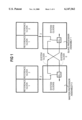
- FIG. 1 is a block diagram showing the synchronization system of the present invention in a master/slave processor arrangement
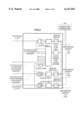
- FIG. 2 is functional block diagram of the synchronization portion
- FIG. 3 is a circuit diagram showing the activated operating mode
- FIG. 4 is a circuit diagram showing the standby mode
- FIG. 5 is a circuit diagram showing the circuit in the monitor mode.
- FIG. 1 shows the basic structure of the mutual clock synchronization.
- a respective PLL is contained in an assembly, a switch that serves for switching between the operating modes "Master” and “Slave” of an assembly being present at the input thereof.
- the Slave Assembly synchronizes to the Master Processor assembly with a PLL (Phase Locked Loop).
- PLL Phase Locked Loop
- FIG. 2 shows the basic structure of an inventive synchronization means.
- the synchronization means comprises
- VCO voltage controlled oscillator
- phase detector RV with a following filter (a loop filter) and that is provided for each reference clock, whereby a respective reference clock signal is at the one input R of a phase detector and the system clock is respectively adjacent at the other input V,
- an operations controller (OC; can, for example, be realized by the processor of the assembly and/or by a corresponding logic) unit that controls the switches following the filters such that respectively one of the output signals of the filters is through-connected to the control input of the VCO,
- a delay unit (shown as a delay line) that delays the system clock preceding the input to the phase detector by the running time difference between the reference clock and the system clock.
- the selection of the reference clocks by (analog) switches at the set voltage input of the VCO is for the following reason. Due to the demand of a maximum 5 ns phase difference between the Master and the Slave, no further running time of any switches whatsoever for the selection of an external reference clock is allowed preceding the input of the phase comparator of the "Partner Processor Assembly" other than the line running time (the time difference between the minimum and the maximum running time of such a switch, namely, deteriorates the worst case phase difference between the Master assembly and the Slave assembly). A separate phase comparator is therefore inventively present for each reference clock.
- a delay unit (which here is a delay line) is inserted preceding the comparison input V of the phase detector of the Partner Processing Assembly that delays the system clock preceding the input to the phase detector by the running time difference between the reference clock on the Master assembly and the system clock of the Slave assembly.
- the operating control also controls further switches (shown in FIGS. 3-5) such that, given a filter whose output signal is not through-connected to the input of the VCO, the output signal is fed back to the one filter input and the decoupled signal of the control input of the VCO is applied to the other filter input.
- the output signal of a passively co-running loop filter is constantly regulated to the same level as that of the active arrangement.
- An optimum transient response of the PLL phase skip thereby derives after the switching to a different reference clock (external reference clock or system clock of the Partner assembly)! A mode switching and/or a change of the external clock source is thus possible without deterioration of the micro-synchronous operation.
- the inventive clock synchronization works without exchange of the phase information. This is achieved in that the line running time between the two processor assemblies is compensated with a lead of the PLL.
- the selected PLL has a zero phase difference at the input of a phase detector (PD) between the local clock and the external reference clock.
- PD phase detector
- phase detector PD-Type 4 from Roland Best, theory und für des Phase-locked Loops, ISBN 3-85502-132-5 can be taken as a phase detector and can be easily modified so that it synchronizes to the positive signal edge and the two outputs can be switched to tri-state.
- the advantage of this type is:
- a slow transient response is required when switching to an external reference.
- the modulation of the set voltage input of the VCO must therefore be small (small amplification) at the input phase skip.
- a fast transient response is required when switching to the Partner processor assembly.
- the modulation of the set voltage input of the VCO must therefore be great (great amplification) at the input phase skip.
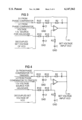
- FIG. 3 shows the activated operating mode
- the PLL control circuit In this operating mode, the PLL control circuit is closed (D1 and U1 are not applied to tri-state).
- the processor assembly can thereby be in Master mode or Slave mode.
- FIG. 4 shows the holdover operating mode
- the processor assembly In this operating mode, the processor assembly is in the Master mode and works without an external reference. In this operating mode, the output of the loop filter amounts to 1.5 V.
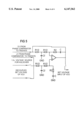
- FIG. 5 shows the monitor VCO operating mode
- the output voltage value of the loop filter corresponds to the voltage value at the VCO set voltage input.
- the correct output level is assured at the VCO set voltage input at the moment of switching to the activated mode (PLL control circuit) (an output level at the positive or negative detent of the operational amplifier would result in a frequency skip that could lead to the upward transgression of the 5 ns maximum phase difference demand between two processor assemblies).
Landscapes
- Stabilization Of Oscillater, Synchronisation, Frequency Synthesizers (AREA)
- Synchronisation In Digital Transmission Systems (AREA)
Applications Claiming Priority (2)
| Application Number | Priority Date | Filing Date | Title |
|---|---|---|---|
| EP96118915 | 1996-11-26 | ||
| PCT/EP1997/006080 WO1998024185A1 (de) | 1996-11-26 | 1997-11-04 | Synchronisationseinrichtung einer baugruppe |
Publications (1)
| Publication Number | Publication Date |
|---|---|
| US6147562A true US6147562A (en) | 2000-11-14 |
Family
ID=8223432
Family Applications (1)
| Application Number | Title | Priority Date | Filing Date |
|---|---|---|---|
| US09/308,947 Expired - Fee Related US6147562A (en) | 1996-11-26 | 1997-11-04 | Apparatus for synchronizing master and slave processors |
Country Status (6)
| Country | Link |
|---|---|
| US (1) | US6147562A (de) |
| EP (1) | EP0941580B1 (de) |
| CN (1) | CN1126255C (de) |
| CA (1) | CA2272658A1 (de) |
| DE (1) | DE59706267D1 (de) |
| WO (1) | WO1998024185A1 (de) |
Cited By (4)
| Publication number | Priority date | Publication date | Assignee | Title |
|---|---|---|---|---|
| US6717484B2 (en) * | 2001-06-29 | 2004-04-06 | Motorola, Inc. | Circuits for use in radio communications |
| WO2007124788A1 (de) * | 2006-01-10 | 2007-11-08 | Rohde & Schwarz Gmbh & Co. Kg | Anordnung zur phasensynchronisation nach dem master/slave-prinzip |
| US20100134159A1 (en) * | 2008-11-28 | 2010-06-03 | Zarlink Semiconductor Inc. | Soft reference switch for phase locked loop |
| US7826519B1 (en) * | 2005-05-23 | 2010-11-02 | Marvell International, Ltd | Method and apparatus for providing coherent phase noise in transceivers or similar systems |
Families Citing this family (1)
| Publication number | Priority date | Publication date | Assignee | Title |
|---|---|---|---|---|
| CN102075314A (zh) * | 2009-11-24 | 2011-05-25 | 航天信息股份有限公司 | 网络税控系统时间同步方法 |
Citations (6)
| Publication number | Priority date | Publication date | Assignee | Title |
|---|---|---|---|---|
| US4511859A (en) * | 1982-08-30 | 1985-04-16 | At&T Bell Laboratories | Apparatus for generating a common output signal as a function of any of a plurality of diverse input signals |
| EP0139126A2 (de) * | 1981-06-08 | 1985-05-02 | BRITISH TELECOMMUNICATIONS public limited company | Phasenriegelschleifen und diese enthaltende elektrische Netzwerke |
| EP0175888A2 (de) * | 1984-09-25 | 1986-04-02 | Siemens Telecomunicazioni S.P.A. | Schaltung zur Begrenzung von momentanen Phasenschwankungen während des Schaltens |
| EP0262481A2 (de) * | 1986-09-30 | 1988-04-06 | Siemens Aktiengesellschaft | Schaltungsanordnung zur Erzeugung eines zu einer zugeführten Referenzfrequenz frequenzsynchronen Taktsignals |
| US5216387A (en) * | 1991-09-10 | 1993-06-01 | John Fluke Mfg. Co., Inc. | Noise reduction method and apparatus for phase-locked loops |
| US5739727A (en) * | 1995-10-05 | 1998-04-14 | Telefonaktiebolaget Lm Ericsson | Sampled phase locked loop being locked with support from another phase locked loop |
-
1997
- 1997-11-04 CA CA002272658A patent/CA2272658A1/en not_active Abandoned
- 1997-11-04 WO PCT/EP1997/006080 patent/WO1998024185A1/de not_active Ceased
- 1997-11-04 CN CN97180095.2A patent/CN1126255C/zh not_active Expired - Fee Related
- 1997-11-04 US US09/308,947 patent/US6147562A/en not_active Expired - Fee Related
- 1997-11-04 EP EP97950088A patent/EP0941580B1/de not_active Expired - Lifetime
- 1997-11-04 DE DE59706267T patent/DE59706267D1/de not_active Expired - Fee Related
Patent Citations (6)
| Publication number | Priority date | Publication date | Assignee | Title |
|---|---|---|---|---|
| EP0139126A2 (de) * | 1981-06-08 | 1985-05-02 | BRITISH TELECOMMUNICATIONS public limited company | Phasenriegelschleifen und diese enthaltende elektrische Netzwerke |
| US4511859A (en) * | 1982-08-30 | 1985-04-16 | At&T Bell Laboratories | Apparatus for generating a common output signal as a function of any of a plurality of diverse input signals |
| EP0175888A2 (de) * | 1984-09-25 | 1986-04-02 | Siemens Telecomunicazioni S.P.A. | Schaltung zur Begrenzung von momentanen Phasenschwankungen während des Schaltens |
| EP0262481A2 (de) * | 1986-09-30 | 1988-04-06 | Siemens Aktiengesellschaft | Schaltungsanordnung zur Erzeugung eines zu einer zugeführten Referenzfrequenz frequenzsynchronen Taktsignals |
| US5216387A (en) * | 1991-09-10 | 1993-06-01 | John Fluke Mfg. Co., Inc. | Noise reduction method and apparatus for phase-locked loops |
| US5739727A (en) * | 1995-10-05 | 1998-04-14 | Telefonaktiebolaget Lm Ericsson | Sampled phase locked loop being locked with support from another phase locked loop |
Cited By (8)
| Publication number | Priority date | Publication date | Assignee | Title |
|---|---|---|---|---|
| US6717484B2 (en) * | 2001-06-29 | 2004-04-06 | Motorola, Inc. | Circuits for use in radio communications |
| EP1271788A3 (de) * | 2001-06-29 | 2004-10-20 | Motorola, Inc. | Schaltungen zur Funkkommunikation |
| US7826519B1 (en) * | 2005-05-23 | 2010-11-02 | Marvell International, Ltd | Method and apparatus for providing coherent phase noise in transceivers or similar systems |
| WO2007124788A1 (de) * | 2006-01-10 | 2007-11-08 | Rohde & Schwarz Gmbh & Co. Kg | Anordnung zur phasensynchronisation nach dem master/slave-prinzip |
| US20090096536A1 (en) * | 2006-01-10 | 2009-04-16 | Rhode & Schwarz Gmbh & Co. Kg | Arrangement for Phase Synchronization According to the Master/Slave Principle |
| US7772928B2 (en) | 2006-01-10 | 2010-08-10 | Rohde & Schwarz Gmbh & Co. Kg | Arrangement for phase synchronization according to the master/slave principle |
| US20100134159A1 (en) * | 2008-11-28 | 2010-06-03 | Zarlink Semiconductor Inc. | Soft reference switch for phase locked loop |
| US7965115B2 (en) | 2008-11-28 | 2011-06-21 | Zarlink Semiconductor Inc. | Soft reference switch for phase locked loop |
Also Published As
| Publication number | Publication date |
|---|---|
| DE59706267D1 (de) | 2002-03-14 |
| EP0941580A1 (de) | 1999-09-15 |
| CN1238863A (zh) | 1999-12-15 |
| WO1998024185A1 (de) | 1998-06-04 |
| EP0941580B1 (de) | 2002-01-30 |
| CN1126255C (zh) | 2003-10-29 |
| CA2272658A1 (en) | 1998-06-04 |
Similar Documents
| Publication | Publication Date | Title |
|---|---|---|
| JP3255418B2 (ja) | ディジタル制御の水晶発振器 | |
| JP2003051742A (ja) | クロック生成回路 | |
| JP3615734B2 (ja) | 基準クロック信号に周波数同期されたクロック信号を生成する回路装置 | |
| KR20070049566A (ko) | 스위치가능 pll 회로 | |
| US5530726A (en) | Method and apparatus for switching of duplexed clock system | |
| US6147562A (en) | Apparatus for synchronizing master and slave processors | |
| KR100212139B1 (ko) | 클럭공급장치 | |
| KR940002449B1 (ko) | 다중 주파수 디지탈 위상 동기 루프 및 이 루프에서 위상 및 주파수를 조정하는 방법 | |
| US20070229128A1 (en) | Clock supply device | |
| US5867545A (en) | Phase-locked loop circuit | |
| KR100328757B1 (ko) | 전송시스템의 클럭신호 전환에 의한 오류방지 장치 | |
| KR20000061197A (ko) | 복수의 위상동기루프를 이용한 클록 주파수 제어장치 및 방법 | |
| JP2725530B2 (ja) | クロック供給方式 | |
| KR100282410B1 (ko) | 시스템 클록 보드 | |
| JPH0267820A (ja) | 標準周波数クロック発生装置 | |
| KR100262945B1 (ko) | 천이모드를이용한디지털위상고정루프의동기제어방법 | |
| JPH0964732A (ja) | 同期クロック生成回路 | |
| JP3160904B2 (ja) | 位相同期発振回路装置 | |
| KR920003362B1 (ko) | 미세 위상차 보정회로 및 보정 방법 | |
| KR100518439B1 (ko) | 이중화된 클럭 모듈의 위상 동기화 장치 | |
| JP2002359552A (ja) | 移動通信基地局装置のクロック同期システム及び方法 | |
| KR100328761B1 (ko) | 광통신 시스템의 시스템 클럭 유니트 스위칭 장치 | |
| KR19980085920A (ko) | 절체 클락동기 및 위상보상회로 | |
| JPH10187272A (ja) | クロック系の冗長構成における位相制御方式 | |
| KR940002451B1 (ko) | 위상 동기루프용 동기검출기 및 동기상태 검출방법 |
Legal Events
| Date | Code | Title | Description |
|---|---|---|---|
| AS | Assignment |
Owner name: SIEMENS AKTIENGESELLSCHAFT, GERMANY Free format text: ASSIGNMENT OF ASSIGNORS INTEREST;ASSIGNOR:QUIRMBACH, GERHARD;REEL/FRAME:010079/0170 Effective date: 19971020 |
|
| FEPP | Fee payment procedure |
Free format text: PAYOR NUMBER ASSIGNED (ORIGINAL EVENT CODE: ASPN); ENTITY STATUS OF PATENT OWNER: LARGE ENTITY |
|
| FPAY | Fee payment |
Year of fee payment: 4 |
|
| AS | Assignment |
Owner name: NOKIA SIEMENS NETWORKS GMBH & CO. KG, GERMANY Free format text: ASSIGNMENT OF ASSIGNORS INTEREST;ASSIGNOR:SIEMENS AKTIENGESELLSCHAFT;REEL/FRAME:020593/0160 Effective date: 20080107 |
|
| REMI | Maintenance fee reminder mailed | ||
| LAPS | Lapse for failure to pay maintenance fees | ||
| STCH | Information on status: patent discontinuation |
Free format text: PATENT EXPIRED DUE TO NONPAYMENT OF MAINTENANCE FEES UNDER 37 CFR 1.362 |
|
| FP | Lapsed due to failure to pay maintenance fee |
Effective date: 20081114 |