US6150915A - Magnetic components and their production - Google Patents
Magnetic components and their production Download PDFInfo
- Publication number
- US6150915A US6150915A US09/215,172 US21517298A US6150915A US 6150915 A US6150915 A US 6150915A US 21517298 A US21517298 A US 21517298A US 6150915 A US6150915 A US 6150915A
- Authority
- US
- United States
- Prior art keywords
- magnetic
- component
- conductor
- magnetic plate
- plates
- Prior art date
- Legal status (The legal status is an assumption and is not a legal conclusion. Google has not performed a legal analysis and makes no representation as to the accuracy of the status listed.)
- Expired - Lifetime
Links
- 238000004519 manufacturing process Methods 0.000 title description 13
- 239000004020 conductor Substances 0.000 claims abstract description 48
- 238000000034 method Methods 0.000 claims abstract description 31
- 238000004804 winding Methods 0.000 claims abstract description 16
- 230000008569 process Effects 0.000 claims abstract description 8
- 238000009413 insulation Methods 0.000 claims abstract description 5
- 239000000696 magnetic material Substances 0.000 claims description 11
- 239000000463 material Substances 0.000 claims description 6
- 229910001030 Iron–nickel alloy Inorganic materials 0.000 claims description 3
- 239000010410 layer Substances 0.000 description 22
- 238000000059 patterning Methods 0.000 description 10
- 238000010276 construction Methods 0.000 description 5
- RYGMFSIKBFXOCR-UHFFFAOYSA-N Copper Chemical compound [Cu] RYGMFSIKBFXOCR-UHFFFAOYSA-N 0.000 description 2
- 229910052802 copper Inorganic materials 0.000 description 2
- 239000010949 copper Substances 0.000 description 2
- 239000012212 insulator Substances 0.000 description 2
- 238000003475 lamination Methods 0.000 description 2
- 235000014676 Phragmites communis Nutrition 0.000 description 1
- 229910000831 Steel Inorganic materials 0.000 description 1
- 238000013459 approach Methods 0.000 description 1
- 230000009286 beneficial effect Effects 0.000 description 1
- 239000012792 core layer Substances 0.000 description 1
- 230000004907 flux Effects 0.000 description 1
- 239000011888 foil Substances 0.000 description 1
- 230000006872 improvement Effects 0.000 description 1
- 229910000889 permalloy Inorganic materials 0.000 description 1
- 238000007747 plating Methods 0.000 description 1
- 230000009467 reduction Effects 0.000 description 1
- 239000010959 steel Substances 0.000 description 1
Images


Classifications
-
- H—ELECTRICITY
- H01—ELECTRIC ELEMENTS
- H01F—MAGNETS; INDUCTANCES; TRANSFORMERS; SELECTION OF MATERIALS FOR THEIR MAGNETIC PROPERTIES
- H01F41/00—Apparatus or processes specially adapted for manufacturing or assembling magnets, inductances or transformers; Apparatus or processes specially adapted for manufacturing materials characterised by their magnetic properties
- H01F41/02—Apparatus or processes specially adapted for manufacturing or assembling magnets, inductances or transformers; Apparatus or processes specially adapted for manufacturing materials characterised by their magnetic properties for manufacturing cores, coils, or magnets
- H01F41/04—Apparatus or processes specially adapted for manufacturing or assembling magnets, inductances or transformers; Apparatus or processes specially adapted for manufacturing materials characterised by their magnetic properties for manufacturing cores, coils, or magnets for manufacturing coils
- H01F41/041—Printed circuit coils
- H01F41/046—Printed circuit coils structurally combined with ferromagnetic material
-
- H—ELECTRICITY
- H01—ELECTRIC ELEMENTS
- H01F—MAGNETS; INDUCTANCES; TRANSFORMERS; SELECTION OF MATERIALS FOR THEIR MAGNETIC PROPERTIES
- H01F17/00—Fixed inductances of the signal type
- H01F17/0006—Printed inductances
- H01F17/0013—Printed inductances with stacked layers
-
- H—ELECTRICITY
- H01—ELECTRIC ELEMENTS
- H01F—MAGNETS; INDUCTANCES; TRANSFORMERS; SELECTION OF MATERIALS FOR THEIR MAGNETIC PROPERTIES
- H01F41/00—Apparatus or processes specially adapted for manufacturing or assembling magnets, inductances or transformers; Apparatus or processes specially adapted for manufacturing materials characterised by their magnetic properties
- H01F41/02—Apparatus or processes specially adapted for manufacturing or assembling magnets, inductances or transformers; Apparatus or processes specially adapted for manufacturing materials characterised by their magnetic properties for manufacturing cores, coils, or magnets
- H01F41/04—Apparatus or processes specially adapted for manufacturing or assembling magnets, inductances or transformers; Apparatus or processes specially adapted for manufacturing materials characterised by their magnetic properties for manufacturing cores, coils, or magnets for manufacturing coils
- H01F41/041—Printed circuit coils
- H01F41/045—Trimming
Definitions
- the invention relates to construction of magnetic components such as inductors and transformers, and to methods for producing them.
- One object is to provide a construction of magnetic component which provides good performance characteristics and which has a relatively flat profile.
- Another object is that the component be easily integrated into a circuit board.
- Another object is to provide a component production method which involves using conventional multilayer printed circuit board production techniques.
- a still further object is to provide improved flexibility in choice of operating characteristics set by design and manufacturing parameters.
- a magnetic component comprising:
- the component comprises an insulating layer and a magnetic plate on both sides of the conductor.
- the magnetic plates are interconnected by magnetic material to provide a closed core.
- the magnetic plates are interconnected by plated through holes.
- the magnetic plate comprises a plurality of isolated sections.
- corresponding sections on both sides of the component are interconnected by magnetic material.
- the sections are shaped as disc sectors.
- the sectors are shaped as quadrants.
- the magnetic plate is of NiFe material.
- the component comprises a plurality of magnetic plates separated by insulation on a side of the conductor.
- the invention provides a method of producing a magnetic component, the method comprising the steps of:
- This method produces a magnetic component having excellent inductance characteristics. Also, by applying the magnetic plate in a pattern as described, the characteristics of the component may be set in a very simple and predictable manner.
- a plurality of conductors and associated insulating layers are formed, and the patterned magnetic plate is applied over an outer conductor.
- an insulating layer and a magnetic plate are applied on both sides of the conductor.
- the magnetic plates are interconnected with magnetic material to provide a closed core.
- the plates are interconnected by plated through holes isolated from the conductor.
- the magnetic plate is applied as a plurality of isolated sections.
- the sections are shaped as disc sectors.
- the conductor. the insulating layer and the magnetic plate are applied in steps for producing a multilayer circuit board whereby the component is integrated into the board.
- FIG. 1 is a diagrammatic cross-sectional view of a magnetic component of the invention
- FIG. 2 is a set of plan views showing parts of the component of FIG. 1 in more detail;
- FIG. 3 is a plan view of an alternative magnetic plate for a magnetic component of the invention.
- FIG. 4 is a diagrammatic cross-sectional view of an alternative magnetic component of the invention.
- FIG. 5 is a set of plan views showing parts of the component of FIG. 4 in more detail
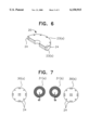
- FIG. 6 is a diagrammatic perspective view showing a magnetic component of FIG. 4.
- FIG. 7 is a set of plan views of parts of a still further construction of magnetic component of the invention.
- FIGS. 1 and 2 there is shown a magnetic component 1 of the invention.
- the component 1 is integrated in a multilayer printed circuit board. It is produced using conventional multilayer printed circuit board production techniques because of the construction of the component itself. These production techniques are conventional and are not described in this document and instead the construction of the components is described in detail, from which it is clear why conventional multilayer circuit production techniques may be used.
- the component 1 comprises a "prepreg" insulator 2 which supports two planar conductors 3(a) and 3(b), each of which is in the shape of a spiral winding as shown in FIG. 2.
- the insulator 2 insulates the windings of the conductors 3(a) and 3(b).
- the component 1 also comprises patterned magnetic plates 4(a) and 4(b) at the top and bottom sides of the component 1.
- the conductors 3(a) and 3(b) comprise leads 5(a) and 5(b) respectively and a through-hole connection so that they are interconnected.
- the conductors 3(a) and 3(b) are of copper material and they provide the windings of the component 1.
- the magnetic plates 4(a) and 4(b) are of NiFe ("permalloy") material.
- the component 1 is produced by sequentially applying a conductor 3(a) or 3(b), an insulating layer, and subsequently a magnetic layer 4(a) or 4(b). These operations are performed in both directions to provide the symmetrical structure illustrated.
- the structure may not be symmetrical and may include only one magnetic plate.
- the component may have a single conductor, a single insulating layer over the conductor, and a single patterned magnetic plate over the insulating layer.
- the component may comprise a number of conductor/insulating layer pairs. It will be appreciated that the overall structure of the component is achieved by using conventional multilayer printed circuit board production techniques by simply bonding various layers as required to provide the component configuration.
- the presence of the patterned magnetic plates 4(a) and 4(b) enhances inductance by providing a low reluctance path to magnetic flux around the conductor windings.
- the inductance characteristics of the component may be controlled by the choice of configuration of the or each magnetic plate. This provides a highly active and predictable level of control in a simple manner because it is achieved by simple plating and patterning steps.
- the magnetic plate may be patterned to comprise a number of isolated sections. In this way, there is no complete path for eddy-currents to flow in opposition to currents flowing in the conductors windings.
- the purpose of patterning in this way is to disrupt eddy current flow so as to help prevent inductance reduction with frequency.
- a magnetic plate 10 comprises four isolated quadrant-shaped sectors 11 separated by radially extending gaps 12.
- the number of sections may be varied to set the inductance characteristics of the component. There is, of course, a trade off between the number of sections and the area of magnetic plate provided and an optimum configuration can be easily found for each type of component.
- the invention provides for setting of inductance characteristics of the component by configuring the manner in which the magnetic plate is patterned over the insulation. This configuration may be achieved by using simple and conventional patterning techniques which are well know in the multilayer printed circuit board production industry.
- FIGS. 4 to 7 inclusive Another option which is available to set the inductance characteristics is to provide a closed core by interconnecting the magnetic plates of both sides of the component.
- FIGS. 4 to 7 inclusive Such a scenario is illustrated in FIGS. 4 to 7 inclusive.
- a magnetic component 20 comprising insulation 21 and a pair of copper conductors 22(a) and 22(b) in a spiral configuration, as for the component 1 shown in FIG. 1.
- the component 20 also comprises magnetic plates 23(a) and 23(b) which are interconnected by through holes 24 which are plated with magnetic material.
- FIG. 7 magnetic plates 30(a) and 30(b) are illustrated which comprise four quadrants as for the magnetic plate 10 shown in FIG. 3.
- the magnetic plates 30(a) and 30(b) are used with conductor windings 31(a) and 31(b).
- the invention provides a very simple method for producing a magnetic component because conventional PCB processing techniques may be used. Also, the invention provides excellent control at the production stage because operating characteristics within a wide frequency range may be chosen by configuring the magnetic plate or plates as appropriate. This is achieved using conventional patterning techniques. Particularly good results are achieved at lower frequencies. At higher frequencies the inductance drops due to the conductivity of the magnetic plates, however, due to the magnetic plate patterning the results still represent an improvement over a component without magnetic material. Also, the invention achieves a component having a relatively flat profile.
- the conductor windings comprise a two-layer circular spiral with 13 turns per layer.
- the spiral has a track width and spacing of 100 ⁇ m and an outer diameter of 8.5 mm.
- the magnetic layer has a circular outline with an outer diameter of 10 mm.
- the top and bottom magnetic layers are divided into four quadrants.
- the results for 1 kHz illustrate how beneficial it is to pattern the magnetic layers and use magnetic plated through holes.
- the inductance increases from 4.4 ⁇ H to 93 ⁇ H for a patterned closed core.
- the inductance is lower at higher frequencies, however, patterning achieves a performance comparable with components with no magnetic material.
- the production method may therefore be applied for a wide component frequency range.
- the magnetic plates may be configured using conventional processing techniques to any shape or configuration desired to achieve the required inductance for the frequency of operation.
- the layers may be applied in any suitable manner instead of bonding, such as by lamination.
- multiple magnetic plates may be applied on each side, insulated from each other. This will provide a method to obtain high inductance values across a wide frequency range.
- further patterning may be carried out in order to trim inductance values, e.g. by using a laser. This type of patterning could be carried out in order to improve inductance tolerance or to provide in-circuit tuning of the component.
Landscapes
- Engineering & Computer Science (AREA)
- Power Engineering (AREA)
- Manufacturing & Machinery (AREA)
- Microelectronics & Electronic Packaging (AREA)
- Coils Or Transformers For Communication (AREA)
- Manufacturing Cores, Coils, And Magnets (AREA)
Priority Applications (1)
| Application Number | Priority Date | Filing Date | Title |
|---|---|---|---|
| US09/493,238 US6320204B1 (en) | 1997-12-25 | 2000-01-28 | Electro-optical device in which an extending portion of a channel region of a semiconductor layer is connected to a capacitor line and an electronic apparatus including the electro-optical device |
Applications Claiming Priority (2)
| Application Number | Priority Date | Filing Date | Title |
|---|---|---|---|
| IES970893 | 1997-12-18 | ||
| IE970893 | 1997-12-18 |
Related Child Applications (1)
| Application Number | Title | Priority Date | Filing Date |
|---|---|---|---|
| US09/219,708 Continuation-In-Part US6066860A (en) | 1997-12-25 | 1998-12-23 | Substrate for electro-optical apparatus, electro-optical apparatus, method for driving electro-optical apparatus, electronic device and projection display device |
Publications (1)
| Publication Number | Publication Date |
|---|---|
| US6150915A true US6150915A (en) | 2000-11-21 |
Family
ID=11041660
Family Applications (1)
| Application Number | Title | Priority Date | Filing Date |
|---|---|---|---|
| US09/215,172 Expired - Lifetime US6150915A (en) | 1997-12-18 | 1998-12-18 | Magnetic components and their production |
Country Status (3)
| Country | Link |
|---|---|
| US (1) | US6150915A (fr) |
| EP (1) | EP0926689A3 (fr) |
| JP (1) | JPH11273951A (fr) |
Cited By (8)
| Publication number | Priority date | Publication date | Assignee | Title |
|---|---|---|---|---|
| US6731193B2 (en) * | 2001-01-27 | 2004-05-04 | Phoenix Contact Gmbh & Co. Kg | Printed circuit board-based current sensor |
| US20050046535A1 (en) * | 2003-09-02 | 2005-03-03 | Kuo-Chi Chiu | Precise multi-pole magnetic component and manufacturing method thereof |
| US7518480B1 (en) | 2006-08-03 | 2009-04-14 | Rf Micro Devices, Inc. | Printed circuit board inductor |
| US20100035785A1 (en) * | 1997-01-09 | 2010-02-11 | Advanced Technology Materials Inc. | Aqueous cleaning composition containing copper-specific corrosion inhibitor for cleaning inorganic residues on semiconductor substrate |
| US20140266546A1 (en) * | 2013-03-15 | 2014-09-18 | Hengchun Mao | High Density Packaging for Efficient Power Processing with a Magnetic Part |
| US20160042861A1 (en) * | 2014-08-07 | 2016-02-11 | Ibiden Co., Ltd. | Printed wiring board |
| US20160163442A1 (en) * | 2014-12-08 | 2016-06-09 | Samsung Electro-Mechanics Co., Ltd. | Electronic component |
| US20180012697A1 (en) * | 2016-07-07 | 2018-01-11 | Samsung Electro-Mechanics Co., Ltd. | Coil component |
Families Citing this family (6)
| Publication number | Priority date | Publication date | Assignee | Title |
|---|---|---|---|---|
| FI20000442A7 (fi) * | 2000-02-25 | 2001-08-26 | Benefon Oyj | Induktiosilmukka |
| ITTO20001128A1 (it) * | 2000-12-04 | 2002-06-04 | Fiat Ricerche | Induttore planare con nucleo ferromagnetico e relativo metodo di fabbricazione. |
| JP2003158017A (ja) * | 2001-11-21 | 2003-05-30 | Jhc Osaka:Kk | トランス |
| JP2007503716A (ja) * | 2003-08-26 | 2007-02-22 | コーニンクレッカ フィリップス エレクトロニクス エヌ ヴィ | 極薄フレキシブル・インダクタ |
| US20070001796A1 (en) * | 2003-08-26 | 2007-01-04 | Eberhardt Waffenschmidt | Printed circuit board with integrated inductor |
| DE102020206989A1 (de) | 2020-06-04 | 2021-12-09 | Robert Bosch Gesellschaft mit beschränkter Haftung | Schaltungsträger für eine elektronische Schaltung und Verfahren zur Herstellung des Schaltungsträgers |
Citations (9)
| Publication number | Priority date | Publication date | Assignee | Title |
|---|---|---|---|---|
| US3898595A (en) * | 1970-11-02 | 1975-08-05 | Cunningham Corp | Magnetic printed circuit |
| JPS5766522A (en) * | 1980-10-13 | 1982-04-22 | Hitachi Ltd | Thin-film magnetic head |
| JPS6175510A (ja) * | 1984-09-21 | 1986-04-17 | Kangiyou Denki Kiki Kk | 小形トランス |
| JPS61216314A (ja) * | 1985-03-20 | 1986-09-26 | Toko Inc | 積層インダクタのトリミング方法 |
| JPH06215962A (ja) * | 1993-01-13 | 1994-08-05 | Hitachi Ltd | トランス |
| US5552756A (en) * | 1993-01-13 | 1996-09-03 | Murata Manufacturing Co., Ltd. | Chip-type common mode choke coil |
| US5726615A (en) * | 1994-03-24 | 1998-03-10 | Bloom; Gordon E. | Integrated-magnetic apparatus |
| US5745981A (en) * | 1993-04-01 | 1998-05-05 | General Electric Company | Method for making magnetic and electromagnetic circuit components having embedded magnetic materials in a high density interconnect structure |
| US5781091A (en) * | 1995-07-24 | 1998-07-14 | Autosplice Systems Inc. | Electronic inductive device and method for manufacturing |
-
1998
- 1998-12-16 EP EP98650088A patent/EP0926689A3/fr not_active Withdrawn
- 1998-12-18 JP JP10375934A patent/JPH11273951A/ja active Pending
- 1998-12-18 US US09/215,172 patent/US6150915A/en not_active Expired - Lifetime
Patent Citations (9)
| Publication number | Priority date | Publication date | Assignee | Title |
|---|---|---|---|---|
| US3898595A (en) * | 1970-11-02 | 1975-08-05 | Cunningham Corp | Magnetic printed circuit |
| JPS5766522A (en) * | 1980-10-13 | 1982-04-22 | Hitachi Ltd | Thin-film magnetic head |
| JPS6175510A (ja) * | 1984-09-21 | 1986-04-17 | Kangiyou Denki Kiki Kk | 小形トランス |
| JPS61216314A (ja) * | 1985-03-20 | 1986-09-26 | Toko Inc | 積層インダクタのトリミング方法 |
| JPH06215962A (ja) * | 1993-01-13 | 1994-08-05 | Hitachi Ltd | トランス |
| US5552756A (en) * | 1993-01-13 | 1996-09-03 | Murata Manufacturing Co., Ltd. | Chip-type common mode choke coil |
| US5745981A (en) * | 1993-04-01 | 1998-05-05 | General Electric Company | Method for making magnetic and electromagnetic circuit components having embedded magnetic materials in a high density interconnect structure |
| US5726615A (en) * | 1994-03-24 | 1998-03-10 | Bloom; Gordon E. | Integrated-magnetic apparatus |
| US5781091A (en) * | 1995-07-24 | 1998-07-14 | Autosplice Systems Inc. | Electronic inductive device and method for manufacturing |
Non-Patent Citations (1)
| Title |
|---|
| Yamaguchi et al, Characteristics of a Thin Film Microtransformer . . . , IEEE Transactions on Magnetics, vol. 29, No. 5, Sep. 1993. * |
Cited By (13)
| Publication number | Priority date | Publication date | Assignee | Title |
|---|---|---|---|---|
| US20100035785A1 (en) * | 1997-01-09 | 2010-02-11 | Advanced Technology Materials Inc. | Aqueous cleaning composition containing copper-specific corrosion inhibitor for cleaning inorganic residues on semiconductor substrate |
| US6731193B2 (en) * | 2001-01-27 | 2004-05-04 | Phoenix Contact Gmbh & Co. Kg | Printed circuit board-based current sensor |
| US7114237B2 (en) * | 2003-09-02 | 2006-10-03 | Industrial Technology Research Institute | Manufacturing method for precise multi-pole magnetic components |
| US20060038646A1 (en) * | 2003-09-02 | 2006-02-23 | Industrial Technology Research Institute | Precise multi-pole magnetic component and manufacturing method thereof |
| US7656259B2 (en) * | 2003-09-02 | 2010-02-02 | Industrial Technology Research Institute | Precise multi-pole magnetic component |
| US20050046535A1 (en) * | 2003-09-02 | 2005-03-03 | Kuo-Chi Chiu | Precise multi-pole magnetic component and manufacturing method thereof |
| US7884690B2 (en) | 2003-09-02 | 2011-02-08 | Industrial Technology Research Institute | Precise multi-pole magnetic component |
| US7518480B1 (en) | 2006-08-03 | 2009-04-14 | Rf Micro Devices, Inc. | Printed circuit board inductor |
| US20140266546A1 (en) * | 2013-03-15 | 2014-09-18 | Hengchun Mao | High Density Packaging for Efficient Power Processing with a Magnetic Part |
| US20160042861A1 (en) * | 2014-08-07 | 2016-02-11 | Ibiden Co., Ltd. | Printed wiring board |
| US20160163442A1 (en) * | 2014-12-08 | 2016-06-09 | Samsung Electro-Mechanics Co., Ltd. | Electronic component |
| US20180012697A1 (en) * | 2016-07-07 | 2018-01-11 | Samsung Electro-Mechanics Co., Ltd. | Coil component |
| US10923259B2 (en) * | 2016-07-07 | 2021-02-16 | Samsung Electro-Mechanics Co., Ltd. | Coil component |
Also Published As
| Publication number | Publication date |
|---|---|
| JPH11273951A (ja) | 1999-10-08 |
| EP0926689A3 (fr) | 1999-12-01 |
| EP0926689A2 (fr) | 1999-06-30 |
Similar Documents
| Publication | Publication Date | Title |
|---|---|---|
| EP1547100B1 (fr) | Dispositifs electroniques de type transformateur/inducteur et leurs procedes de production | |
| US6820321B2 (en) | Method of making electronic transformer/inductor devices | |
| EP0926689A2 (fr) | Composants magnétiques et leurs production | |
| JP2016515305A (ja) | ラミネートポリマーを使用するプレーナ磁気技術に関する装置および方法 | |
| US4959630A (en) | High-frequency transformer | |
| US9329249B2 (en) | MRIS shim coil | |
| US5134770A (en) | Method of fabricating a high-frequency transformer | |
| JP2010123879A (ja) | コイル構造体及びその製造方法 | |
| US3505569A (en) | Inductive circuit component | |
| JPH056829A (ja) | 薄型トランス | |
| US9111678B2 (en) | Planar core-type uniform external field equalizer and fabrication | |
| IE981060A1 (en) | Magnetic components and their production | |
| CN114974802A (zh) | 一种磁性器件、谐振电路及led驱动电源 | |
| JPH07201575A (ja) | 板状巻き線およびその製造方法 | |
| JPS59114807A (ja) | プリント多層コイル | |
| JPS62176112A (ja) | 高周波コイル | |
| JP2004221177A (ja) | コイル部品 | |
| JPS6222416A (ja) | プリント配線板上へのコイルとトランスの製造方法 | |
| JP2004221178A (ja) | コイル部品の製造方法 | |
| JPH10208941A (ja) | チップインダクタとその製造方法 | |
| JPH08264359A (ja) | 小型電磁石及びその製造方法 | |
| HK1079896B (en) | Electronic transformer/inductor devices and methods for making same | |
| KR19990031211A (ko) | 트랜스포머의 필름코일 연결방법 | |
| JPH0234901A (ja) | 電気部品 | |
| JP2000201045A (ja) | 電源フィルタ |
Legal Events
| Date | Code | Title | Description |
|---|---|---|---|
| AS | Assignment |
Owner name: NATIONAL UNIVERSITY OF IRELAND, CORK, IRELAND Free format text: ASSIGNMENT OF ASSIGNORS INTEREST;ASSIGNORS:O'REILLY, STEPHEN;DUFFY, MAEVE;O'DONNELL, TERENCE;AND OTHERS;REEL/FRAME:009779/0090 Effective date: 19981214 |
|
| STCF | Information on status: patent grant |
Free format text: PATENTED CASE |
|
| FPAY | Fee payment |
Year of fee payment: 4 |
|
| FPAY | Fee payment |
Year of fee payment: 8 |
|
| FPAY | Fee payment |
Year of fee payment: 12 |