US6204565B1 - Semiconductor carrier and method for manufacturing the same - Google Patents
Semiconductor carrier and method for manufacturing the same Download PDFInfo
- Publication number
- US6204565B1 US6204565B1 US09/329,838 US32983899A US6204565B1 US 6204565 B1 US6204565 B1 US 6204565B1 US 32983899 A US32983899 A US 32983899A US 6204565 B1 US6204565 B1 US 6204565B1
- Authority
- US
- United States
- Prior art keywords
- hole
- adhesive
- interconnection pattern
- semiconductor carrier
- support substrate
- Prior art date
- Legal status (The legal status is an assumption and is not a legal conclusion. Google has not performed a legal analysis and makes no representation as to the accuracy of the status listed.)
- Expired - Lifetime
Links
- 0 *C(=C)C(=O)OCC(O)CO[Ar]OCC(O)CO[Ar]OCC(O)COC(=O)C(*)=C.*c1cc(C2(c3ccc(C)c(*)c3)c3ccccc3-c3ccccc32)ccc1C Chemical compound *C(=C)C(=O)OCC(O)CO[Ar]OCC(O)CO[Ar]OCC(O)COC(=O)C(*)=C.*c1cc(C2(c3ccc(C)c(*)c3)c3ccccc3-c3ccccc32)ccc1C 0.000 description 1
Images


Classifications
-
- H—ELECTRICITY
- H10—SEMICONDUCTOR DEVICES; ELECTRIC SOLID-STATE DEVICES NOT OTHERWISE PROVIDED FOR
- H10W—GENERIC PACKAGES, INTERCONNECTIONS, CONNECTORS OR OTHER CONSTRUCTIONAL DETAILS OF DEVICES COVERED BY CLASS H10
- H10W70/00—Package substrates; Interposers; Redistribution layers [RDL]
- H10W70/60—Insulating or insulated package substrates; Interposers; Redistribution layers
- H10W70/67—Insulating or insulated package substrates; Interposers; Redistribution layers characterised by their insulating layers or insulating parts
- H10W70/69—Insulating materials thereof
-
- H—ELECTRICITY
- H10—SEMICONDUCTOR DEVICES; ELECTRIC SOLID-STATE DEVICES NOT OTHERWISE PROVIDED FOR
- H10W—GENERIC PACKAGES, INTERCONNECTIONS, CONNECTORS OR OTHER CONSTRUCTIONAL DETAILS OF DEVICES COVERED BY CLASS H10
- H10W70/00—Package substrates; Interposers; Redistribution layers [RDL]
- H10W70/01—Manufacture or treatment
- H10W70/05—Manufacture or treatment of insulating or insulated package substrates, or of interposers, or of redistribution layers
- H10W70/093—Connecting or disconnecting other interconnections thereto or therefrom, e.g. connecting bond wires or bumps
-
- H—ELECTRICITY
- H10—SEMICONDUCTOR DEVICES; ELECTRIC SOLID-STATE DEVICES NOT OTHERWISE PROVIDED FOR
- H10W—GENERIC PACKAGES, INTERCONNECTIONS, CONNECTORS OR OTHER CONSTRUCTIONAL DETAILS OF DEVICES COVERED BY CLASS H10
- H10W70/00—Package substrates; Interposers; Redistribution layers [RDL]
- H10W70/01—Manufacture or treatment
- H10W70/05—Manufacture or treatment of insulating or insulated package substrates, or of interposers, or of redistribution layers
- H10W70/095—Manufacture or treatment of insulating or insulated package substrates, or of interposers, or of redistribution layers of vias therein
-
- H—ELECTRICITY
- H10—SEMICONDUCTOR DEVICES; ELECTRIC SOLID-STATE DEVICES NOT OTHERWISE PROVIDED FOR
- H10W—GENERIC PACKAGES, INTERCONNECTIONS, CONNECTORS OR OTHER CONSTRUCTIONAL DETAILS OF DEVICES COVERED BY CLASS H10
- H10W72/00—Interconnections or connectors in packages
- H10W72/071—Connecting or disconnecting
- H10W72/072—Connecting or disconnecting of bump connectors
- H10W72/07251—Connecting or disconnecting of bump connectors characterised by changes in properties of the bump connectors during connecting
-
- H—ELECTRICITY
- H10—SEMICONDUCTOR DEVICES; ELECTRIC SOLID-STATE DEVICES NOT OTHERWISE PROVIDED FOR
- H10W—GENERIC PACKAGES, INTERCONNECTIONS, CONNECTORS OR OTHER CONSTRUCTIONAL DETAILS OF DEVICES COVERED BY CLASS H10
- H10W72/00—Interconnections or connectors in packages
- H10W72/20—Bump connectors, e.g. solder bumps or copper pillars; Dummy bumps; Thermal bumps
-
- H—ELECTRICITY
- H10—SEMICONDUCTOR DEVICES; ELECTRIC SOLID-STATE DEVICES NOT OTHERWISE PROVIDED FOR
- H10W—GENERIC PACKAGES, INTERCONNECTIONS, CONNECTORS OR OTHER CONSTRUCTIONAL DETAILS OF DEVICES COVERED BY CLASS H10
- H10W72/00—Interconnections or connectors in packages
- H10W72/90—Bond pads, in general
- H10W72/921—Structures or relative sizes of bond pads
- H10W72/922—Bond pads being integral with underlying chip-level interconnections
-
- H—ELECTRICITY
- H10—SEMICONDUCTOR DEVICES; ELECTRIC SOLID-STATE DEVICES NOT OTHERWISE PROVIDED FOR
- H10W—GENERIC PACKAGES, INTERCONNECTIONS, CONNECTORS OR OTHER CONSTRUCTIONAL DETAILS OF DEVICES COVERED BY CLASS H10
- H10W72/00—Interconnections or connectors in packages
- H10W72/90—Bond pads, in general
- H10W72/921—Structures or relative sizes of bond pads
- H10W72/923—Bond pads having multiple stacked layers
-
- H—ELECTRICITY
- H10—SEMICONDUCTOR DEVICES; ELECTRIC SOLID-STATE DEVICES NOT OTHERWISE PROVIDED FOR
- H10W—GENERIC PACKAGES, INTERCONNECTIONS, CONNECTORS OR OTHER CONSTRUCTIONAL DETAILS OF DEVICES COVERED BY CLASS H10
- H10W72/00—Interconnections or connectors in packages
- H10W72/90—Bond pads, in general
- H10W72/941—Dispositions of bond pads
- H10W72/9415—Dispositions of bond pads relative to the surface, e.g. recessed, protruding
Definitions
- the present invention relates to a semiconductor carrier suitable for mounting a semiconductor device with a high density and method for manufacturing the same.
- FIG. 4 depicts a cross section of the carrier, in which a copper interconnection pattern 41 , a base layer 42 consisting of a polyimide film, and an adhesive layer 43 consisting of a thermoplastic polyimide construct a tape substrate 44 .
- a through hole bump 45 to be connected electrically with a chip is formed in the tape substrate 44 .
- a cover resist layer 48 which includes an aperture 46 for connecting the semiconductor carrier with a mount board electrically and a slit 47 for bonding, is formed on the copper interconnection pattern 41 .
- a substance of the adhesive layer 43 and a technology for forming a through hole in the base layer 42 and adhesive layer 43 to form the through hole bump 45 greatly affect the performance and reliability of the semiconductor carrier.
- Essential properties required for the adhesive layer 43 are an advantageous heat resistance, moisture resistance, adhesion and low stress which enable to endure various treatments suffered from post-processes such as a process for mounting the semiconductor carrier on the mount board as well as a drug resistance without degrading its characteristics through plating and cleaning processes.
- the through hole forming method for forming the through hole bump 45 also greatly affects the performance and reliability of the semiconductor carrier.
- a method using a laser such as an excimer, carbonic acid gas or YAG laser is generally well known as the through hole forming method.
- process conditions are unstable so that an etching remainder or sludge may be left on the via bottom.
- the method further includes a disadvantage that a reliable bump can not be formed because a thermal damage is given to a surface of the copper interconnection pattern 41 according to a type of the laser, resulting in an unstable adhesion of the interface between the copper interconnection pattern 41 and the through hole bump 45 .
- the formation of the through hole by the laser reduces the throughput and makes a limitation for the yield.
- it is not suitable for the mass production and is disadvantageous with respect to the cost.
- the carbonic acid gas laser and YAG laser are difficult to form a fine through hole because of their long wavelengths. It is desirable for the method as the means to solve such the disadvantages that the adhesive layer 43 has a photosensitivity and that the through hole is formed by the conventional photolithography process.
- the semiconductor carrier with an adhesive that has the advantageous heat resistance, moisture resistance, adhesion, low stress and drug resistance as described above.
- the adhesive should also have the photosensitivity and advantageous resolution, and enable to form a fine through hole by the conventional photolithography process.
- the known adhesives with photosensitivity include those of polyimide series as disclosed in JPA 4-337380 and those of epoxy series as disclosed in JPA 6-19134 and JPA 6-27660.
- the photosensitive adhesive of polyimide series has a particularly large contraction stress caused during setting.
- the stress affects to bend the semiconductor carrier unfavorably, and prevents a practical semiconductor carrier to be formed.
- the photosensitive adhesive of epoxy series is difficult to form a reliable semiconductor carrier because of its essential disadvantage in the heat resistance and moisture resistance. In addition, it has a low resolution and is not suitable for forming the fine through hole.
- An object of the present invention is to solve the above disadvantages.
- the present invention is provided with a semiconductor carrier having a bump formed by coating a photosensitive adhesive consisting of an epoxy acrylate having a fluorene skeleton or polybenzoxazole over a support substrate having a conductive interconnection pattern, exposing and developing the adhesive for forming a through hole therein, and plating for filling a metal within the through hole.
- a photosensitive adhesive consisting of an epoxy acrylate having a fluorene skeleton or polybenzoxazole
- the epoxy acrylate having a fluorene skeleton preferably comprises a material represented by the following general formula (I):
- R is a hydrogen atom or low-grade alkyl group
- n is an integer of 0-20.
- the polybenzoxazole is preferably selected from those disclosed in JPA 5-11451 and JPA 5-11452.
- the epoxy acrylate having a fluorene skeleton and the polybenzoxazole are the most suitable for the use of the above photosensitive adhesive because they have an advantageous heat resistance, moisture resistance, adhesion and drug resistance. They also have a low stress because of their small contraction during setting. They further enable to form a fine through hole by the conventional photolithography process because of their photosensitivity.
- the photosensitive adhesive is the epoxy acrylate having a fluorene skeleton, coating it on a support substrate having a conductive interconnection pattern, opening a hole in it by exposing and developing processes, and thereafter heating it at a temperature of 80-160° C. or at a temperature of 80-250° C. if the photosensitive adhesive is the polybenzoxazole.
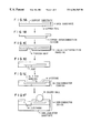
- FIGS. 1A-1F show a process diagram of an example of a manufacturing process of a semiconductor carrier of the present invention
- FIG. 2 is a graph showing a relationship between a heating temperature and an adhesive force when an epoxy acrylate having a fluorene skeleton is used as a photosensitive adhesive;
- FIG. 3 is a graph showing a relationship between a heating temperature and an adhesive force when a polybenzoxazole is used as a photosensitive adhesive.
- FIG. 4 is a schematic cross sectional view of a semiconductor carrier in the art.
- FIGS. 1A-1F show a process diagram of an example of a manufacturing process of a semiconductor carrier having a bump formed by coating a photosensitive adhesive over a support substrate having a conductive interconnection pattern, exposing and developing the adhesive for forming a through hole therein, and plating for filling a metal within the through hole.
- a base substrate 3 that consists of a support substrate 1 and a copper foil 2 is prepared first (FIG. 1 ( a )).
- the copper foil 2 is etched into a predetermined shape by a photolithography process to form a copper interconnection pattern 4 (FIG. 1 ( b )).
- a liquid photosensitive adhesive 5 consisting of an epoxy acrylate having a fluorene skeleton or polybenzoxazole is coated next over a surface of the copper interconnection pattern 4 by a method such as spin coating, die coating, curtain coating and printing. It is then dried at 75° C. for 20 minutes. Thereafter, it is exposed at 600 mJ/cm 2 and developed by dipping in an aqueous solution of 1% sodium carbonate for 3 minutes to form a through hole 6 (FIG. 1 ( c )).
- the photosensitive adhesive may also be a dry film type.
- Such photosensitive adhesive 5 of the dry film type is laminated on the surface of the copper interconnection pattern 4 with heating, thereafter exposed and developed to form the through hole 6 as well as in the case of the liquid type. Then, filling the through hole 6 with a metal by the plating method or the like may form a bump 7 (FIG. 1 ( d )).
- a semiconductor carrier 10 is finally obtained by forming, on the support substrate 1 , an aperture 8 for mounting a solder ball 13 or the like and a slit 9 for bonding, with a chemical etching or laser technology (FIG. 1 ( e )).
- the support substrate 1 is made of any material that enables to form the aperture 8 and the bonding slit 9 by the chemical etching or laser technology, such as a polyimide film, epoxy film, glass cloth immersed printed circuit board and aramid non-woven cloth immersed printed circuit board which have suitably excellent workability.
- the photosensitive adhesive 5 consisting of an epoxy acrylate having a fluorene skeleton or polybenzoxazole has an excellent resolution and thus is advantageous in forming the fine through hole 6 with a high aspect ratio. It is confirmed that the bump 7 has an excellent reliability of a junction with the copper interconnection pattern 4 . This is because no damage to the copper interconnection pattern 4 is caused and no remainder and residue of the bottom of the through hole 6 is present, which are caused when the laser is used.
- Coupling a semiconductor substrate 11 with the photosensitive adhesive 5 mechanically and making a junction between an electrode 12 of the semiconductor substrate 11 and the bump 7 electrically may fabricate a semiconductor device 14 , as shown in FIG. 1 ( f ), which has an excellent reliability because the photosensitive adhesive 5 has the advantageous heat resistance, moisture resistance, adhesion and drug resistance.
- the photosensitive adhesive 5 may absorb moisture, promote the degradation by the post-process such as the plating process and reduce the adhesion to the semiconductor substrate 11 in the worst case.
- the inventors found that performing a heat treatment after the formation of the photosensitive adhesive 5 having the through hole 6 and prior to the plating process to form the bump 7 may prevent the degradation of the characteristics due to the post-processes including the plating process with sustaining the adhesion of the adhesive, and can form the semiconductor carrier excellent for fabricating the semiconductor device. In this case, conditions for the heat treatment are important.
- FIG. 2 shows a relationship between an adhesive force (peel strength) to the semiconductor substrate 11 and a heating time (process time: 30 minutes) when the epoxy acrylate having a fluorene skeleton is used as the photosensitive adhesive 5 .
- the peel strength exhibits 800 g/cm without heating and reduces sharply at heating temperatures of 160° C. or more.
- a heat treatment at heating temperatures of 80° C. or less can not achieve the original object to improve the degradation of the characteristics.
- the heat treatment at 80-160° C. is optimum prior to the plating process if the photosensitive adhesive 5 comprises the epoxy acrylate having a fluorene skeleton.
- the heat treatment at 80-250° C. is similarly optimum if the photosensitive adhesive 5 comprises the polybenzoxazole as obvious from a relationship between a heating temperature and adhesion shown in FIG. 3 .
- the bump is formed by coating the photosensitive adhesive consisting of an epoxy acrylate having a fluorene skeleton or polybenzoxazole over a support substrate having a conductive interconnection pattern, exposing and developing the adhesive for forming a through hole therein, and plating for filling a metal within the through hole. Therefore, the excellent reliable semiconductor device can be formed. In addition, it is extremely useful for a miniaturized pitch connection because the fine through hole bump can be easily formed.
- the photosensitive adhesive comprises the epoxy acrylate having a fluorene skeleton, coating it on a support substrate having a conductive interconnection pattern, opening a hole in it by exposing and developing processes, and thereafter heating it at a temperature of 80-160° C. or at a temperature of 80-250° C. if the photosensitive adhesive is the polybenzoxazole.
- an advantageous semiconductor carrier may be obtained which can sustain the adhesion of the adhesive, prevent the degradation of characteristics due to the affection from the post-process such as the plating process, and fabricate the semiconductor device with ease.
Landscapes
- Adhesives Or Adhesive Processes (AREA)
- Wire Bonding (AREA)
- Die Bonding (AREA)
Applications Claiming Priority (2)
| Application Number | Priority Date | Filing Date | Title |
|---|---|---|---|
| JP16209198A JP3178417B2 (ja) | 1998-06-10 | 1998-06-10 | 半導体キャリアおよびその製造方法 |
| JP10-162091 | 1998-06-10 |
Publications (1)
| Publication Number | Publication Date |
|---|---|
| US6204565B1 true US6204565B1 (en) | 2001-03-20 |
Family
ID=15747914
Family Applications (1)
| Application Number | Title | Priority Date | Filing Date |
|---|---|---|---|
| US09/329,838 Expired - Lifetime US6204565B1 (en) | 1998-06-10 | 1999-06-10 | Semiconductor carrier and method for manufacturing the same |
Country Status (2)
| Country | Link |
|---|---|
| US (1) | US6204565B1 (ja) |
| JP (1) | JP3178417B2 (ja) |
Cited By (7)
| Publication number | Priority date | Publication date | Assignee | Title |
|---|---|---|---|---|
| US6444403B1 (en) * | 1999-05-20 | 2002-09-03 | Nec Corporation | Resin laminated wiring sheet, wiring structure using the same, and production method thereof |
| US20030045024A1 (en) * | 2001-09-03 | 2003-03-06 | Tadanori Shimoto | Interconnecting substrate for carrying semiconductor device, method of producing thereof and package of semiconductor device |
| US20030149207A1 (en) * | 2001-07-31 | 2003-08-07 | Andreas Walter | Use of polybenzoxazoles (PBOS) for adhesion |
| US20050088833A1 (en) * | 2002-05-27 | 2005-04-28 | Katsumi Kikuchi | Semiconductor device mounting board, method of manufacturing the same, method of inspecting the same, and semiconductor package |
| US20080044664A1 (en) * | 2004-05-21 | 2008-02-21 | Jsr Corporation | Laminated Body and Semiconductor Drive |
| US20110091811A1 (en) * | 2009-10-16 | 2011-04-21 | Samsung Electronics Co., Ltd. | Double-layered patternable adhesive film, method of forming the same, and method of forming patternable adhesive layer using the same |
| US20140349446A1 (en) * | 2006-03-21 | 2014-11-27 | Promerus, Llc | Methods and materials useful for chip stacking, chip and wafer bonding |
Families Citing this family (2)
| Publication number | Priority date | Publication date | Assignee | Title |
|---|---|---|---|---|
| JP2003008221A (ja) * | 2001-06-19 | 2003-01-10 | Ibiden Co Ltd | 多層プリント配線板および多層プリント配線板の製造方法 |
| TW201707959A (zh) * | 2015-08-21 | 2017-03-01 | Jsr股份有限公司 | 基材的處理方法、暫時固定用組成物及半導體裝置 |
Citations (15)
| Publication number | Priority date | Publication date | Assignee | Title |
|---|---|---|---|---|
| JPS5922393A (ja) | 1982-07-29 | 1984-02-04 | 日本電気株式会社 | プリント配線板およびその製造方法 |
| US4769399A (en) * | 1987-03-12 | 1988-09-06 | Minnesota Mining And Manufacturing Company | Epoxy adhesive film for electronic applications |
| JPH03177034A (ja) | 1989-12-05 | 1991-08-01 | Casio Comput Co Ltd | 電子部品の接続方法 |
| JPH04292611A (ja) | 1991-03-20 | 1992-10-16 | Nippon Steel Corp | エポキシアクリレート樹脂系成形材料 |
| JPH04337380A (ja) | 1991-05-15 | 1992-11-25 | Sumitomo Bakelite Co Ltd | 耐熱感光性ポリイミド接着剤 |
| JPH0511452A (ja) | 1991-07-05 | 1993-01-22 | Sumitomo Bakelite Co Ltd | ポジ型感光性樹脂組成物 |
| JPH0511451A (ja) | 1991-07-05 | 1993-01-22 | Sumitomo Bakelite Co Ltd | ポジ型感光性樹脂組成物 |
| JPH05259223A (ja) | 1992-03-11 | 1993-10-08 | Nec Corp | フィルムキャリアテープ |
| JPH05327224A (ja) | 1992-05-22 | 1993-12-10 | Dainippon Printing Co Ltd | 多層配線基板の製造方法及びその製造方法で製造される多層配線基板 |
| JPH0619134A (ja) | 1992-06-30 | 1994-01-28 | Tamura Kaken Kk | 感光性樹脂組成物 |
| JPH0627660A (ja) | 1992-07-07 | 1994-02-04 | Nippon Oil Co Ltd | 感光性組成物 |
| JPH06334343A (ja) | 1992-09-04 | 1994-12-02 | Hitachi Ltd | 多層配線基板の製造方法および高密度多層配線基板 |
| JPH09116267A (ja) | 1995-09-25 | 1997-05-02 | Internatl Business Mach Corp <Ibm> | バイアを有する多層回路基板の製造方法、チップ・キャリアおよびチップ・キャリアの製造方法 |
| JPH09214141A (ja) | 1995-11-29 | 1997-08-15 | Nec Corp | 配線構造 |
| JPH09219590A (ja) | 1996-02-13 | 1997-08-19 | Hitachi Ltd | 薄膜積層基板用シートならびに薄膜積層基板、およびそれらの製造方法ならびに製造装置 |
-
1998
- 1998-06-10 JP JP16209198A patent/JP3178417B2/ja not_active Expired - Fee Related
-
1999
- 1999-06-10 US US09/329,838 patent/US6204565B1/en not_active Expired - Lifetime
Patent Citations (15)
| Publication number | Priority date | Publication date | Assignee | Title |
|---|---|---|---|---|
| JPS5922393A (ja) | 1982-07-29 | 1984-02-04 | 日本電気株式会社 | プリント配線板およびその製造方法 |
| US4769399A (en) * | 1987-03-12 | 1988-09-06 | Minnesota Mining And Manufacturing Company | Epoxy adhesive film for electronic applications |
| JPH03177034A (ja) | 1989-12-05 | 1991-08-01 | Casio Comput Co Ltd | 電子部品の接続方法 |
| JPH04292611A (ja) | 1991-03-20 | 1992-10-16 | Nippon Steel Corp | エポキシアクリレート樹脂系成形材料 |
| JPH04337380A (ja) | 1991-05-15 | 1992-11-25 | Sumitomo Bakelite Co Ltd | 耐熱感光性ポリイミド接着剤 |
| JPH0511452A (ja) | 1991-07-05 | 1993-01-22 | Sumitomo Bakelite Co Ltd | ポジ型感光性樹脂組成物 |
| JPH0511451A (ja) | 1991-07-05 | 1993-01-22 | Sumitomo Bakelite Co Ltd | ポジ型感光性樹脂組成物 |
| JPH05259223A (ja) | 1992-03-11 | 1993-10-08 | Nec Corp | フィルムキャリアテープ |
| JPH05327224A (ja) | 1992-05-22 | 1993-12-10 | Dainippon Printing Co Ltd | 多層配線基板の製造方法及びその製造方法で製造される多層配線基板 |
| JPH0619134A (ja) | 1992-06-30 | 1994-01-28 | Tamura Kaken Kk | 感光性樹脂組成物 |
| JPH0627660A (ja) | 1992-07-07 | 1994-02-04 | Nippon Oil Co Ltd | 感光性組成物 |
| JPH06334343A (ja) | 1992-09-04 | 1994-12-02 | Hitachi Ltd | 多層配線基板の製造方法および高密度多層配線基板 |
| JPH09116267A (ja) | 1995-09-25 | 1997-05-02 | Internatl Business Mach Corp <Ibm> | バイアを有する多層回路基板の製造方法、チップ・キャリアおよびチップ・キャリアの製造方法 |
| JPH09214141A (ja) | 1995-11-29 | 1997-08-15 | Nec Corp | 配線構造 |
| JPH09219590A (ja) | 1996-02-13 | 1997-08-19 | Hitachi Ltd | 薄膜積層基板用シートならびに薄膜積層基板、およびそれらの製造方法ならびに製造装置 |
Non-Patent Citations (2)
| Title |
|---|
| 1996 Electronic Components and Technology Conference pp. 727-732, "Development of Molded Fine-Pitch Ball Grid Array (FPBGA) Using Through-Hole Bonding Process", Matsuda et al. |
| Abstract-pub-No. SU 598916A, Derwent database, Feb. 1978, one page, Akutin et al.* |
Cited By (13)
| Publication number | Priority date | Publication date | Assignee | Title |
|---|---|---|---|---|
| US6444403B1 (en) * | 1999-05-20 | 2002-09-03 | Nec Corporation | Resin laminated wiring sheet, wiring structure using the same, and production method thereof |
| US20030149207A1 (en) * | 2001-07-31 | 2003-08-07 | Andreas Walter | Use of polybenzoxazoles (PBOS) for adhesion |
| US7052936B2 (en) | 2001-07-31 | 2006-05-30 | Infineon Technologies Ag | Use of polybenzoxazoles (PBOS) for adhesion |
| US20030045024A1 (en) * | 2001-09-03 | 2003-03-06 | Tadanori Shimoto | Interconnecting substrate for carrying semiconductor device, method of producing thereof and package of semiconductor device |
| US6861757B2 (en) * | 2001-09-03 | 2005-03-01 | Nec Corporation | Interconnecting substrate for carrying semiconductor device, method of producing thereof and package of semiconductor device |
| US7338884B2 (en) | 2001-09-03 | 2008-03-04 | Nec Corporation | Interconnecting substrate for carrying semiconductor device, method of producing thereof and package of semiconductor device |
| US7474538B2 (en) * | 2002-05-27 | 2009-01-06 | Nec Corporation | Semiconductor device mounting board, method of manufacturing the same, method of inspecting the same, and semiconductor package |
| US20050088833A1 (en) * | 2002-05-27 | 2005-04-28 | Katsumi Kikuchi | Semiconductor device mounting board, method of manufacturing the same, method of inspecting the same, and semiconductor package |
| US20080044664A1 (en) * | 2004-05-21 | 2008-02-21 | Jsr Corporation | Laminated Body and Semiconductor Drive |
| US7608928B2 (en) * | 2004-05-21 | 2009-10-27 | Jsr Corporation | Laminated body and semiconductor device |
| US20140349446A1 (en) * | 2006-03-21 | 2014-11-27 | Promerus, Llc | Methods and materials useful for chip stacking, chip and wafer bonding |
| US9263416B2 (en) * | 2006-03-21 | 2016-02-16 | Sumitomo Bakelite Co., Ltd. | Methods and materials useful for chip stacking, chip and wafer bonding |
| US20110091811A1 (en) * | 2009-10-16 | 2011-04-21 | Samsung Electronics Co., Ltd. | Double-layered patternable adhesive film, method of forming the same, and method of forming patternable adhesive layer using the same |
Also Published As
| Publication number | Publication date |
|---|---|
| JP3178417B2 (ja) | 2001-06-18 |
| JPH11354591A (ja) | 1999-12-24 |
Similar Documents
| Publication | Publication Date | Title |
|---|---|---|
| US6822320B2 (en) | Microelectronic connection components utilizing conductive cores and polymeric coatings | |
| US6218281B1 (en) | Semiconductor device with flip chip bonding pads and manufacture thereof | |
| US7223652B2 (en) | Capacitor and manufacturing method thereof, semiconductor device and substrate for a semiconductor device | |
| JP2830903B2 (ja) | 半導体デバイスの製造方法 | |
| US7755183B2 (en) | Wiring board, method of manufacturing the same, and semiconductor device | |
| EP0536418B1 (en) | Method of manufacturing a semiconductor device terminal structure | |
| US6461892B2 (en) | Methods of making a connection component using a removable layer | |
| US6543674B2 (en) | Multilayer interconnection and method | |
| JPH10504137A (ja) | 一体的にバンプされた電子パッケージコンポーネント | |
| KR100682284B1 (ko) | 반도체 장치 제조 방법 | |
| US6204565B1 (en) | Semiconductor carrier and method for manufacturing the same | |
| US7402900B2 (en) | Semiconductor device substrate, semiconductor device, and manufacturing method thereof | |
| US6538209B1 (en) | Substrate for mounting semiconductor element having circuit patterns, and an insulating layer made of photosensitive and thermally-melting type adhesive resin | |
| US9231167B2 (en) | Insulation structure for high temperature conditions and manufacturing method thereof | |
| US7087510B2 (en) | Method of making bondable leads using positive photoresist and structures made therefrom | |
| US8048793B2 (en) | Flip chip for electrical function test and manufacturing method thereof | |
| US6333136B1 (en) | Carrier film and process for producing the same | |
| JP2004119773A (ja) | 半導体装置及びその製造方法 | |
| US5095627A (en) | Method for mounting of semiconductor crystals | |
| KR20000062154A (ko) | 전자부품 실장용 필름캐리어 테이프 및 그 제조방법 | |
| KR100511965B1 (ko) | 테이프기판의 주석도금방법 | |
| JP2841888B2 (ja) | 多層配線基板及びその製造方法 | |
| JP3503229B2 (ja) | 半導体装置およびその製造方法 | |
| JPH0521640A (ja) | Icチツプ搭載用基板およびicチツプの搭載方法 | |
| JPH1022324A (ja) | 半導体装置およびその製造方法 |
Legal Events
| Date | Code | Title | Description |
|---|---|---|---|
| AS | Assignment |
Owner name: NEC CORPORATION, JAPAN Free format text: ASSIGNMENT OF ASSIGNORS INTEREST;ASSIGNORS:SHIMOTO, TADANORI;MATSUI, KOJI;REEL/FRAME:010037/0080 Effective date: 19990531 |
|
| FEPP | Fee payment procedure |
Free format text: PAYER NUMBER DE-ASSIGNED (ORIGINAL EVENT CODE: RMPN); ENTITY STATUS OF PATENT OWNER: LARGE ENTITY Free format text: PAYOR NUMBER ASSIGNED (ORIGINAL EVENT CODE: ASPN); ENTITY STATUS OF PATENT OWNER: LARGE ENTITY |
|
| STCF | Information on status: patent grant |
Free format text: PATENTED CASE |
|
| FPAY | Fee payment |
Year of fee payment: 4 |
|
| FPAY | Fee payment |
Year of fee payment: 8 |
|
| FPAY | Fee payment |
Year of fee payment: 12 |