US7008669B2 - Ceramic and method of manufacturing the same, dielectric capacitor, semiconductor device, and element - Google Patents
Ceramic and method of manufacturing the same, dielectric capacitor, semiconductor device, and element Download PDFInfo
- Publication number
- US7008669B2 US7008669B2 US10/166,707 US16670702A US7008669B2 US 7008669 B2 US7008669 B2 US 7008669B2 US 16670702 A US16670702 A US 16670702A US 7008669 B2 US7008669 B2 US 7008669B2
- Authority
- US
- United States
- Prior art keywords
- raw material
- film
- ceramic
- manufacturing
- ferroelectric
- Prior art date
- Legal status (The legal status is an assumption and is not a legal conclusion. Google has not performed a legal analysis and makes no representation as to the accuracy of the status listed.)
- Expired - Lifetime, expires
Links
Images




Classifications
-
- C—CHEMISTRY; METALLURGY
- C04—CEMENTS; CONCRETE; ARTIFICIAL STONE; CERAMICS; REFRACTORIES
- C04B—LIME, MAGNESIA; SLAG; CEMENTS; COMPOSITIONS THEREOF, e.g. MORTARS, CONCRETE OR LIKE BUILDING MATERIALS; ARTIFICIAL STONE; CERAMICS; REFRACTORIES; TREATMENT OF NATURAL STONE
- C04B35/00—Shaped ceramic products characterised by their composition; Ceramics compositions; Processing powders of inorganic compounds preparatory to the manufacturing of ceramic products
- C04B35/01—Shaped ceramic products characterised by their composition; Ceramics compositions; Processing powders of inorganic compounds preparatory to the manufacturing of ceramic products based on oxide ceramics
- C04B35/453—Shaped ceramic products characterised by their composition; Ceramics compositions; Processing powders of inorganic compounds preparatory to the manufacturing of ceramic products based on oxide ceramics based on zinc, tin, or bismuth oxides or solid solutions thereof with other oxides, e.g. zincates, stannates or bismuthates
- C04B35/457—Shaped ceramic products characterised by their composition; Ceramics compositions; Processing powders of inorganic compounds preparatory to the manufacturing of ceramic products based on oxide ceramics based on zinc, tin, or bismuth oxides or solid solutions thereof with other oxides, e.g. zincates, stannates or bismuthates based on tin oxides or stannates
-
- H—ELECTRICITY
- H10—SEMICONDUCTOR DEVICES; ELECTRIC SOLID-STATE DEVICES NOT OTHERWISE PROVIDED FOR
- H10D—INORGANIC ELECTRIC SEMICONDUCTOR DEVICES
- H10D84/00—Integrated devices formed in or on semiconductor substrates that comprise only semiconducting layers, e.g. on Si wafers or on GaAs-on-Si wafers
- H10D84/80—Integrated devices formed in or on semiconductor substrates that comprise only semiconducting layers, e.g. on Si wafers or on GaAs-on-Si wafers characterised by the integration of at least one component covered by groups H10D12/00 or H10D30/00, e.g. integration of IGFETs
-
- C—CHEMISTRY; METALLURGY
- C04—CEMENTS; CONCRETE; ARTIFICIAL STONE; CERAMICS; REFRACTORIES
- C04B—LIME, MAGNESIA; SLAG; CEMENTS; COMPOSITIONS THEREOF, e.g. MORTARS, CONCRETE OR LIKE BUILDING MATERIALS; ARTIFICIAL STONE; CERAMICS; REFRACTORIES; TREATMENT OF NATURAL STONE
- C04B35/00—Shaped ceramic products characterised by their composition; Ceramics compositions; Processing powders of inorganic compounds preparatory to the manufacturing of ceramic products
- C04B35/01—Shaped ceramic products characterised by their composition; Ceramics compositions; Processing powders of inorganic compounds preparatory to the manufacturing of ceramic products based on oxide ceramics
-
- C—CHEMISTRY; METALLURGY
- C04—CEMENTS; CONCRETE; ARTIFICIAL STONE; CERAMICS; REFRACTORIES
- C04B—LIME, MAGNESIA; SLAG; CEMENTS; COMPOSITIONS THEREOF, e.g. MORTARS, CONCRETE OR LIKE BUILDING MATERIALS; ARTIFICIAL STONE; CERAMICS; REFRACTORIES; TREATMENT OF NATURAL STONE
- C04B35/00—Shaped ceramic products characterised by their composition; Ceramics compositions; Processing powders of inorganic compounds preparatory to the manufacturing of ceramic products
- C04B35/01—Shaped ceramic products characterised by their composition; Ceramics compositions; Processing powders of inorganic compounds preparatory to the manufacturing of ceramic products based on oxide ceramics
- C04B35/16—Shaped ceramic products characterised by their composition; Ceramics compositions; Processing powders of inorganic compounds preparatory to the manufacturing of ceramic products based on oxide ceramics based on silicates other than clay
-
- C—CHEMISTRY; METALLURGY
- C04—CEMENTS; CONCRETE; ARTIFICIAL STONE; CERAMICS; REFRACTORIES
- C04B—LIME, MAGNESIA; SLAG; CEMENTS; COMPOSITIONS THEREOF, e.g. MORTARS, CONCRETE OR LIKE BUILDING MATERIALS; ARTIFICIAL STONE; CERAMICS; REFRACTORIES; TREATMENT OF NATURAL STONE
- C04B35/00—Shaped ceramic products characterised by their composition; Ceramics compositions; Processing powders of inorganic compounds preparatory to the manufacturing of ceramic products
- C04B35/01—Shaped ceramic products characterised by their composition; Ceramics compositions; Processing powders of inorganic compounds preparatory to the manufacturing of ceramic products based on oxide ceramics
- C04B35/42—Shaped ceramic products characterised by their composition; Ceramics compositions; Processing powders of inorganic compounds preparatory to the manufacturing of ceramic products based on oxide ceramics based on chromites
-
- C—CHEMISTRY; METALLURGY
- C04—CEMENTS; CONCRETE; ARTIFICIAL STONE; CERAMICS; REFRACTORIES
- C04B—LIME, MAGNESIA; SLAG; CEMENTS; COMPOSITIONS THEREOF, e.g. MORTARS, CONCRETE OR LIKE BUILDING MATERIALS; ARTIFICIAL STONE; CERAMICS; REFRACTORIES; TREATMENT OF NATURAL STONE
- C04B35/00—Shaped ceramic products characterised by their composition; Ceramics compositions; Processing powders of inorganic compounds preparatory to the manufacturing of ceramic products
- C04B35/01—Shaped ceramic products characterised by their composition; Ceramics compositions; Processing powders of inorganic compounds preparatory to the manufacturing of ceramic products based on oxide ceramics
- C04B35/45—Shaped ceramic products characterised by their composition; Ceramics compositions; Processing powders of inorganic compounds preparatory to the manufacturing of ceramic products based on oxide ceramics based on copper oxide or solid solutions thereof with other oxides
- C04B35/4521—Shaped ceramic products characterised by their composition; Ceramics compositions; Processing powders of inorganic compounds preparatory to the manufacturing of ceramic products based on oxide ceramics based on copper oxide or solid solutions thereof with other oxides containing bismuth oxide
-
- C—CHEMISTRY; METALLURGY
- C04—CEMENTS; CONCRETE; ARTIFICIAL STONE; CERAMICS; REFRACTORIES
- C04B—LIME, MAGNESIA; SLAG; CEMENTS; COMPOSITIONS THEREOF, e.g. MORTARS, CONCRETE OR LIKE BUILDING MATERIALS; ARTIFICIAL STONE; CERAMICS; REFRACTORIES; TREATMENT OF NATURAL STONE
- C04B35/00—Shaped ceramic products characterised by their composition; Ceramics compositions; Processing powders of inorganic compounds preparatory to the manufacturing of ceramic products
- C04B35/01—Shaped ceramic products characterised by their composition; Ceramics compositions; Processing powders of inorganic compounds preparatory to the manufacturing of ceramic products based on oxide ceramics
- C04B35/46—Shaped ceramic products characterised by their composition; Ceramics compositions; Processing powders of inorganic compounds preparatory to the manufacturing of ceramic products based on oxide ceramics based on titanium oxides or titanates
- C04B35/462—Shaped ceramic products characterised by their composition; Ceramics compositions; Processing powders of inorganic compounds preparatory to the manufacturing of ceramic products based on oxide ceramics based on titanium oxides or titanates based on titanates
- C04B35/465—Shaped ceramic products characterised by their composition; Ceramics compositions; Processing powders of inorganic compounds preparatory to the manufacturing of ceramic products based on oxide ceramics based on titanium oxides or titanates based on titanates based on alkaline earth metal titanates
-
- C—CHEMISTRY; METALLURGY
- C04—CEMENTS; CONCRETE; ARTIFICIAL STONE; CERAMICS; REFRACTORIES
- C04B—LIME, MAGNESIA; SLAG; CEMENTS; COMPOSITIONS THEREOF, e.g. MORTARS, CONCRETE OR LIKE BUILDING MATERIALS; ARTIFICIAL STONE; CERAMICS; REFRACTORIES; TREATMENT OF NATURAL STONE
- C04B35/00—Shaped ceramic products characterised by their composition; Ceramics compositions; Processing powders of inorganic compounds preparatory to the manufacturing of ceramic products
- C04B35/01—Shaped ceramic products characterised by their composition; Ceramics compositions; Processing powders of inorganic compounds preparatory to the manufacturing of ceramic products based on oxide ceramics
- C04B35/46—Shaped ceramic products characterised by their composition; Ceramics compositions; Processing powders of inorganic compounds preparatory to the manufacturing of ceramic products based on oxide ceramics based on titanium oxides or titanates
- C04B35/462—Shaped ceramic products characterised by their composition; Ceramics compositions; Processing powders of inorganic compounds preparatory to the manufacturing of ceramic products based on oxide ceramics based on titanium oxides or titanates based on titanates
- C04B35/472—Shaped ceramic products characterised by their composition; Ceramics compositions; Processing powders of inorganic compounds preparatory to the manufacturing of ceramic products based on oxide ceramics based on titanium oxides or titanates based on titanates based on lead titanates
-
- C—CHEMISTRY; METALLURGY
- C04—CEMENTS; CONCRETE; ARTIFICIAL STONE; CERAMICS; REFRACTORIES
- C04B—LIME, MAGNESIA; SLAG; CEMENTS; COMPOSITIONS THEREOF, e.g. MORTARS, CONCRETE OR LIKE BUILDING MATERIALS; ARTIFICIAL STONE; CERAMICS; REFRACTORIES; TREATMENT OF NATURAL STONE
- C04B35/00—Shaped ceramic products characterised by their composition; Ceramics compositions; Processing powders of inorganic compounds preparatory to the manufacturing of ceramic products
- C04B35/01—Shaped ceramic products characterised by their composition; Ceramics compositions; Processing powders of inorganic compounds preparatory to the manufacturing of ceramic products based on oxide ceramics
- C04B35/46—Shaped ceramic products characterised by their composition; Ceramics compositions; Processing powders of inorganic compounds preparatory to the manufacturing of ceramic products based on oxide ceramics based on titanium oxides or titanates
- C04B35/462—Shaped ceramic products characterised by their composition; Ceramics compositions; Processing powders of inorganic compounds preparatory to the manufacturing of ceramic products based on oxide ceramics based on titanium oxides or titanates based on titanates
- C04B35/475—Shaped ceramic products characterised by their composition; Ceramics compositions; Processing powders of inorganic compounds preparatory to the manufacturing of ceramic products based on oxide ceramics based on titanium oxides or titanates based on titanates based on bismuth titanates
-
- C—CHEMISTRY; METALLURGY
- C04—CEMENTS; CONCRETE; ARTIFICIAL STONE; CERAMICS; REFRACTORIES
- C04B—LIME, MAGNESIA; SLAG; CEMENTS; COMPOSITIONS THEREOF, e.g. MORTARS, CONCRETE OR LIKE BUILDING MATERIALS; ARTIFICIAL STONE; CERAMICS; REFRACTORIES; TREATMENT OF NATURAL STONE
- C04B35/00—Shaped ceramic products characterised by their composition; Ceramics compositions; Processing powders of inorganic compounds preparatory to the manufacturing of ceramic products
- C04B35/01—Shaped ceramic products characterised by their composition; Ceramics compositions; Processing powders of inorganic compounds preparatory to the manufacturing of ceramic products based on oxide ceramics
- C04B35/48—Shaped ceramic products characterised by their composition; Ceramics compositions; Processing powders of inorganic compounds preparatory to the manufacturing of ceramic products based on oxide ceramics based on zirconium or hafnium oxides, zirconates, zircon or hafnates
- C04B35/49—Shaped ceramic products characterised by their composition; Ceramics compositions; Processing powders of inorganic compounds preparatory to the manufacturing of ceramic products based on oxide ceramics based on zirconium or hafnium oxides, zirconates, zircon or hafnates containing also titanium oxides or titanates
- C04B35/491—Shaped ceramic products characterised by their composition; Ceramics compositions; Processing powders of inorganic compounds preparatory to the manufacturing of ceramic products based on oxide ceramics based on zirconium or hafnium oxides, zirconates, zircon or hafnates containing also titanium oxides or titanates based on lead zirconates and lead titanates, e.g. PZT
-
- C—CHEMISTRY; METALLURGY
- C04—CEMENTS; CONCRETE; ARTIFICIAL STONE; CERAMICS; REFRACTORIES
- C04B—LIME, MAGNESIA; SLAG; CEMENTS; COMPOSITIONS THEREOF, e.g. MORTARS, CONCRETE OR LIKE BUILDING MATERIALS; ARTIFICIAL STONE; CERAMICS; REFRACTORIES; TREATMENT OF NATURAL STONE
- C04B35/00—Shaped ceramic products characterised by their composition; Ceramics compositions; Processing powders of inorganic compounds preparatory to the manufacturing of ceramic products
- C04B35/01—Shaped ceramic products characterised by their composition; Ceramics compositions; Processing powders of inorganic compounds preparatory to the manufacturing of ceramic products based on oxide ceramics
- C04B35/48—Shaped ceramic products characterised by their composition; Ceramics compositions; Processing powders of inorganic compounds preparatory to the manufacturing of ceramic products based on oxide ceramics based on zirconium or hafnium oxides, zirconates, zircon or hafnates
- C04B35/49—Shaped ceramic products characterised by their composition; Ceramics compositions; Processing powders of inorganic compounds preparatory to the manufacturing of ceramic products based on oxide ceramics based on zirconium or hafnium oxides, zirconates, zircon or hafnates containing also titanium oxides or titanates
- C04B35/491—Shaped ceramic products characterised by their composition; Ceramics compositions; Processing powders of inorganic compounds preparatory to the manufacturing of ceramic products based on oxide ceramics based on zirconium or hafnium oxides, zirconates, zircon or hafnates containing also titanium oxides or titanates based on lead zirconates and lead titanates, e.g. PZT
- C04B35/493—Shaped ceramic products characterised by their composition; Ceramics compositions; Processing powders of inorganic compounds preparatory to the manufacturing of ceramic products based on oxide ceramics based on zirconium or hafnium oxides, zirconates, zircon or hafnates containing also titanium oxides or titanates based on lead zirconates and lead titanates, e.g. PZT containing also other lead compounds
-
- C—CHEMISTRY; METALLURGY
- C04—CEMENTS; CONCRETE; ARTIFICIAL STONE; CERAMICS; REFRACTORIES
- C04B—LIME, MAGNESIA; SLAG; CEMENTS; COMPOSITIONS THEREOF, e.g. MORTARS, CONCRETE OR LIKE BUILDING MATERIALS; ARTIFICIAL STONE; CERAMICS; REFRACTORIES; TREATMENT OF NATURAL STONE
- C04B35/00—Shaped ceramic products characterised by their composition; Ceramics compositions; Processing powders of inorganic compounds preparatory to the manufacturing of ceramic products
- C04B35/01—Shaped ceramic products characterised by their composition; Ceramics compositions; Processing powders of inorganic compounds preparatory to the manufacturing of ceramic products based on oxide ceramics
- C04B35/495—Shaped ceramic products characterised by their composition; Ceramics compositions; Processing powders of inorganic compounds preparatory to the manufacturing of ceramic products based on oxide ceramics based on vanadium, niobium, tantalum, molybdenum or tungsten oxides or solid solutions thereof with other oxides, e.g. vanadates, niobates, tantalates, molybdates or tungstates
-
- C—CHEMISTRY; METALLURGY
- C04—CEMENTS; CONCRETE; ARTIFICIAL STONE; CERAMICS; REFRACTORIES
- C04B—LIME, MAGNESIA; SLAG; CEMENTS; COMPOSITIONS THEREOF, e.g. MORTARS, CONCRETE OR LIKE BUILDING MATERIALS; ARTIFICIAL STONE; CERAMICS; REFRACTORIES; TREATMENT OF NATURAL STONE
- C04B35/00—Shaped ceramic products characterised by their composition; Ceramics compositions; Processing powders of inorganic compounds preparatory to the manufacturing of ceramic products
- C04B35/01—Shaped ceramic products characterised by their composition; Ceramics compositions; Processing powders of inorganic compounds preparatory to the manufacturing of ceramic products based on oxide ceramics
- C04B35/495—Shaped ceramic products characterised by their composition; Ceramics compositions; Processing powders of inorganic compounds preparatory to the manufacturing of ceramic products based on oxide ceramics based on vanadium, niobium, tantalum, molybdenum or tungsten oxides or solid solutions thereof with other oxides, e.g. vanadates, niobates, tantalates, molybdates or tungstates
- C04B35/497—Shaped ceramic products characterised by their composition; Ceramics compositions; Processing powders of inorganic compounds preparatory to the manufacturing of ceramic products based on oxide ceramics based on vanadium, niobium, tantalum, molybdenum or tungsten oxides or solid solutions thereof with other oxides, e.g. vanadates, niobates, tantalates, molybdates or tungstates based on solid solutions with lead oxides
-
- C—CHEMISTRY; METALLURGY
- C04—CEMENTS; CONCRETE; ARTIFICIAL STONE; CERAMICS; REFRACTORIES
- C04B—LIME, MAGNESIA; SLAG; CEMENTS; COMPOSITIONS THEREOF, e.g. MORTARS, CONCRETE OR LIKE BUILDING MATERIALS; ARTIFICIAL STONE; CERAMICS; REFRACTORIES; TREATMENT OF NATURAL STONE
- C04B35/00—Shaped ceramic products characterised by their composition; Ceramics compositions; Processing powders of inorganic compounds preparatory to the manufacturing of ceramic products
- C04B35/622—Forming processes; Processing powders of inorganic compounds preparatory to the manufacturing of ceramic products
- C04B35/624—Sol-gel processing
-
- C—CHEMISTRY; METALLURGY
- C04—CEMENTS; CONCRETE; ARTIFICIAL STONE; CERAMICS; REFRACTORIES
- C04B—LIME, MAGNESIA; SLAG; CEMENTS; COMPOSITIONS THEREOF, e.g. MORTARS, CONCRETE OR LIKE BUILDING MATERIALS; ARTIFICIAL STONE; CERAMICS; REFRACTORIES; TREATMENT OF NATURAL STONE
- C04B35/00—Shaped ceramic products characterised by their composition; Ceramics compositions; Processing powders of inorganic compounds preparatory to the manufacturing of ceramic products
- C04B35/622—Forming processes; Processing powders of inorganic compounds preparatory to the manufacturing of ceramic products
- C04B35/626—Preparing or treating the powders individually or as batches ; preparing or treating macroscopic reinforcing agents for ceramic products, e.g. fibres; mechanical aspects section B
- C04B35/62605—Treating the starting powders individually or as mixtures
- C04B35/62625—Wet mixtures
- C04B35/6264—Mixing media, e.g. organic solvents
-
- C—CHEMISTRY; METALLURGY
- C04—CEMENTS; CONCRETE; ARTIFICIAL STONE; CERAMICS; REFRACTORIES
- C04B—LIME, MAGNESIA; SLAG; CEMENTS; COMPOSITIONS THEREOF, e.g. MORTARS, CONCRETE OR LIKE BUILDING MATERIALS; ARTIFICIAL STONE; CERAMICS; REFRACTORIES; TREATMENT OF NATURAL STONE
- C04B35/00—Shaped ceramic products characterised by their composition; Ceramics compositions; Processing powders of inorganic compounds preparatory to the manufacturing of ceramic products
- C04B35/622—Forming processes; Processing powders of inorganic compounds preparatory to the manufacturing of ceramic products
- C04B35/626—Preparing or treating the powders individually or as batches ; preparing or treating macroscopic reinforcing agents for ceramic products, e.g. fibres; mechanical aspects section B
- C04B35/62605—Treating the starting powders individually or as mixtures
- C04B35/62645—Thermal treatment of powders or mixtures thereof other than sintering
-
- C—CHEMISTRY; METALLURGY
- C04—CEMENTS; CONCRETE; ARTIFICIAL STONE; CERAMICS; REFRACTORIES
- C04B—LIME, MAGNESIA; SLAG; CEMENTS; COMPOSITIONS THEREOF, e.g. MORTARS, CONCRETE OR LIKE BUILDING MATERIALS; ARTIFICIAL STONE; CERAMICS; REFRACTORIES; TREATMENT OF NATURAL STONE
- C04B35/00—Shaped ceramic products characterised by their composition; Ceramics compositions; Processing powders of inorganic compounds preparatory to the manufacturing of ceramic products
- C04B35/622—Forming processes; Processing powders of inorganic compounds preparatory to the manufacturing of ceramic products
- C04B35/64—Burning or sintering processes
-
- C—CHEMISTRY; METALLURGY
- C23—COATING METALLIC MATERIAL; COATING MATERIAL WITH METALLIC MATERIAL; CHEMICAL SURFACE TREATMENT; DIFFUSION TREATMENT OF METALLIC MATERIAL; COATING BY VACUUM EVAPORATION, BY SPUTTERING, BY ION IMPLANTATION OR BY CHEMICAL VAPOUR DEPOSITION, IN GENERAL; INHIBITING CORROSION OF METALLIC MATERIAL OR INCRUSTATION IN GENERAL
- C23C—COATING METALLIC MATERIAL; COATING MATERIAL WITH METALLIC MATERIAL; SURFACE TREATMENT OF METALLIC MATERIAL BY DIFFUSION INTO THE SURFACE, BY CHEMICAL CONVERSION OR SUBSTITUTION; COATING BY VACUUM EVAPORATION, BY SPUTTERING, BY ION IMPLANTATION OR BY CHEMICAL VAPOUR DEPOSITION, IN GENERAL
- C23C14/00—Coating by vacuum evaporation, by sputtering or by ion implantation of the coating forming material
- C23C14/06—Coating by vacuum evaporation, by sputtering or by ion implantation of the coating forming material characterised by the coating material
- C23C14/08—Oxides
-
- C—CHEMISTRY; METALLURGY
- C23—COATING METALLIC MATERIAL; COATING MATERIAL WITH METALLIC MATERIAL; CHEMICAL SURFACE TREATMENT; DIFFUSION TREATMENT OF METALLIC MATERIAL; COATING BY VACUUM EVAPORATION, BY SPUTTERING, BY ION IMPLANTATION OR BY CHEMICAL VAPOUR DEPOSITION, IN GENERAL; INHIBITING CORROSION OF METALLIC MATERIAL OR INCRUSTATION IN GENERAL
- C23C—COATING METALLIC MATERIAL; COATING MATERIAL WITH METALLIC MATERIAL; SURFACE TREATMENT OF METALLIC MATERIAL BY DIFFUSION INTO THE SURFACE, BY CHEMICAL CONVERSION OR SUBSTITUTION; COATING BY VACUUM EVAPORATION, BY SPUTTERING, BY ION IMPLANTATION OR BY CHEMICAL VAPOUR DEPOSITION, IN GENERAL
- C23C16/00—Chemical coating by decomposition of gaseous compounds, without leaving reaction products of surface material in the coating, i.e. chemical vapour deposition [CVD] processes
- C23C16/22—Chemical coating by decomposition of gaseous compounds, without leaving reaction products of surface material in the coating, i.e. chemical vapour deposition [CVD] processes characterised by the deposition of inorganic material, other than metallic material
- C23C16/30—Deposition of compounds, mixtures or solid solutions, e.g. borides, carbides, nitrides
- C23C16/40—Oxides
-
- C—CHEMISTRY; METALLURGY
- C23—COATING METALLIC MATERIAL; COATING MATERIAL WITH METALLIC MATERIAL; CHEMICAL SURFACE TREATMENT; DIFFUSION TREATMENT OF METALLIC MATERIAL; COATING BY VACUUM EVAPORATION, BY SPUTTERING, BY ION IMPLANTATION OR BY CHEMICAL VAPOUR DEPOSITION, IN GENERAL; INHIBITING CORROSION OF METALLIC MATERIAL OR INCRUSTATION IN GENERAL
- C23C—COATING METALLIC MATERIAL; COATING MATERIAL WITH METALLIC MATERIAL; SURFACE TREATMENT OF METALLIC MATERIAL BY DIFFUSION INTO THE SURFACE, BY CHEMICAL CONVERSION OR SUBSTITUTION; COATING BY VACUUM EVAPORATION, BY SPUTTERING, BY ION IMPLANTATION OR BY CHEMICAL VAPOUR DEPOSITION, IN GENERAL
- C23C16/00—Chemical coating by decomposition of gaseous compounds, without leaving reaction products of surface material in the coating, i.e. chemical vapour deposition [CVD] processes
- C23C16/22—Chemical coating by decomposition of gaseous compounds, without leaving reaction products of surface material in the coating, i.e. chemical vapour deposition [CVD] processes characterised by the deposition of inorganic material, other than metallic material
- C23C16/30—Deposition of compounds, mixtures or solid solutions, e.g. borides, carbides, nitrides
- C23C16/40—Oxides
- C23C16/409—Oxides of the type ABO3 with A representing alkali, alkaline earth metal or lead and B representing a refractory metal, nickel, scandium or a lanthanide
-
- C—CHEMISTRY; METALLURGY
- C23—COATING METALLIC MATERIAL; COATING MATERIAL WITH METALLIC MATERIAL; CHEMICAL SURFACE TREATMENT; DIFFUSION TREATMENT OF METALLIC MATERIAL; COATING BY VACUUM EVAPORATION, BY SPUTTERING, BY ION IMPLANTATION OR BY CHEMICAL VAPOUR DEPOSITION, IN GENERAL; INHIBITING CORROSION OF METALLIC MATERIAL OR INCRUSTATION IN GENERAL
- C23C—COATING METALLIC MATERIAL; COATING MATERIAL WITH METALLIC MATERIAL; SURFACE TREATMENT OF METALLIC MATERIAL BY DIFFUSION INTO THE SURFACE, BY CHEMICAL CONVERSION OR SUBSTITUTION; COATING BY VACUUM EVAPORATION, BY SPUTTERING, BY ION IMPLANTATION OR BY CHEMICAL VAPOUR DEPOSITION, IN GENERAL
- C23C18/00—Chemical coating by decomposition of either liquid compounds or solutions of the coating forming compounds, without leaving reaction products of surface material in the coating; Contact plating
- C23C18/02—Chemical coating by decomposition of either liquid compounds or solutions of the coating forming compounds, without leaving reaction products of surface material in the coating; Contact plating by thermal decomposition
- C23C18/12—Chemical coating by decomposition of either liquid compounds or solutions of the coating forming compounds, without leaving reaction products of surface material in the coating; Contact plating by thermal decomposition characterised by the deposition of inorganic material other than metallic material
- C23C18/1204—Chemical coating by decomposition of either liquid compounds or solutions of the coating forming compounds, without leaving reaction products of surface material in the coating; Contact plating by thermal decomposition characterised by the deposition of inorganic material other than metallic material inorganic material, e.g. non-oxide and non-metallic such as sulfides, nitrides based compounds
- C23C18/1208—Oxides, e.g. ceramics
-
- C—CHEMISTRY; METALLURGY
- C23—COATING METALLIC MATERIAL; COATING MATERIAL WITH METALLIC MATERIAL; CHEMICAL SURFACE TREATMENT; DIFFUSION TREATMENT OF METALLIC MATERIAL; COATING BY VACUUM EVAPORATION, BY SPUTTERING, BY ION IMPLANTATION OR BY CHEMICAL VAPOUR DEPOSITION, IN GENERAL; INHIBITING CORROSION OF METALLIC MATERIAL OR INCRUSTATION IN GENERAL
- C23C—COATING METALLIC MATERIAL; COATING MATERIAL WITH METALLIC MATERIAL; SURFACE TREATMENT OF METALLIC MATERIAL BY DIFFUSION INTO THE SURFACE, BY CHEMICAL CONVERSION OR SUBSTITUTION; COATING BY VACUUM EVAPORATION, BY SPUTTERING, BY ION IMPLANTATION OR BY CHEMICAL VAPOUR DEPOSITION, IN GENERAL
- C23C18/00—Chemical coating by decomposition of either liquid compounds or solutions of the coating forming compounds, without leaving reaction products of surface material in the coating; Contact plating
- C23C18/02—Chemical coating by decomposition of either liquid compounds or solutions of the coating forming compounds, without leaving reaction products of surface material in the coating; Contact plating by thermal decomposition
- C23C18/12—Chemical coating by decomposition of either liquid compounds or solutions of the coating forming compounds, without leaving reaction products of surface material in the coating; Contact plating by thermal decomposition characterised by the deposition of inorganic material other than metallic material
- C23C18/1225—Deposition of multilayers of inorganic material
-
- H—ELECTRICITY
- H10—SEMICONDUCTOR DEVICES; ELECTRIC SOLID-STATE DEVICES NOT OTHERWISE PROVIDED FOR
- H10B—ELECTRONIC MEMORY DEVICES
- H10B53/00—Ferroelectric RAM [FeRAM] devices comprising ferroelectric memory capacitors
-
- H—ELECTRICITY
- H10—SEMICONDUCTOR DEVICES; ELECTRIC SOLID-STATE DEVICES NOT OTHERWISE PROVIDED FOR
- H10B—ELECTRONIC MEMORY DEVICES
- H10B53/00—Ferroelectric RAM [FeRAM] devices comprising ferroelectric memory capacitors
- H10B53/30—Ferroelectric RAM [FeRAM] devices comprising ferroelectric memory capacitors characterised by the memory core region
-
- H—ELECTRICITY
- H10—SEMICONDUCTOR DEVICES; ELECTRIC SOLID-STATE DEVICES NOT OTHERWISE PROVIDED FOR
- H10N—ELECTRIC SOLID-STATE DEVICES NOT OTHERWISE PROVIDED FOR
- H10N30/00—Piezoelectric or electrostrictive devices
- H10N30/01—Manufacture or treatment
- H10N30/07—Forming of piezoelectric or electrostrictive parts or bodies on an electrical element or another base
- H10N30/074—Forming of piezoelectric or electrostrictive parts or bodies on an electrical element or another base by depositing piezoelectric or electrostrictive layers, e.g. aerosol or screen printing
- H10N30/077—Forming of piezoelectric or electrostrictive parts or bodies on an electrical element or another base by depositing piezoelectric or electrostrictive layers, e.g. aerosol or screen printing by liquid phase deposition
- H10N30/078—Forming of piezoelectric or electrostrictive parts or bodies on an electrical element or another base by depositing piezoelectric or electrostrictive layers, e.g. aerosol or screen printing by liquid phase deposition by sol-gel deposition
-
- H—ELECTRICITY
- H10—SEMICONDUCTOR DEVICES; ELECTRIC SOLID-STATE DEVICES NOT OTHERWISE PROVIDED FOR
- H10N—ELECTRIC SOLID-STATE DEVICES NOT OTHERWISE PROVIDED FOR
- H10N30/00—Piezoelectric or electrostrictive devices
- H10N30/80—Constructional details
- H10N30/85—Piezoelectric or electrostrictive active materials
- H10N30/853—Ceramic compositions
- H10N30/8561—Bismuth-based oxides
-
- C—CHEMISTRY; METALLURGY
- C04—CEMENTS; CONCRETE; ARTIFICIAL STONE; CERAMICS; REFRACTORIES
- C04B—LIME, MAGNESIA; SLAG; CEMENTS; COMPOSITIONS THEREOF, e.g. MORTARS, CONCRETE OR LIKE BUILDING MATERIALS; ARTIFICIAL STONE; CERAMICS; REFRACTORIES; TREATMENT OF NATURAL STONE
- C04B2235/00—Aspects relating to ceramic starting mixtures or sintered ceramic products
- C04B2235/02—Composition of constituents of the starting material or of secondary phases of the final product
- C04B2235/30—Constituents and secondary phases not being of a fibrous nature
- C04B2235/32—Metal oxides, mixed metal oxides, or oxide-forming salts thereof, e.g. carbonates, nitrates, (oxy)hydroxides, chlorides
- C04B2235/3205—Alkaline earth oxides or oxide forming salts thereof, e.g. beryllium oxide
-
- C—CHEMISTRY; METALLURGY
- C04—CEMENTS; CONCRETE; ARTIFICIAL STONE; CERAMICS; REFRACTORIES
- C04B—LIME, MAGNESIA; SLAG; CEMENTS; COMPOSITIONS THEREOF, e.g. MORTARS, CONCRETE OR LIKE BUILDING MATERIALS; ARTIFICIAL STONE; CERAMICS; REFRACTORIES; TREATMENT OF NATURAL STONE
- C04B2235/00—Aspects relating to ceramic starting mixtures or sintered ceramic products
- C04B2235/02—Composition of constituents of the starting material or of secondary phases of the final product
- C04B2235/30—Constituents and secondary phases not being of a fibrous nature
- C04B2235/32—Metal oxides, mixed metal oxides, or oxide-forming salts thereof, e.g. carbonates, nitrates, (oxy)hydroxides, chlorides
- C04B2235/3205—Alkaline earth oxides or oxide forming salts thereof, e.g. beryllium oxide
- C04B2235/3208—Calcium oxide or oxide-forming salts thereof, e.g. lime
-
- C—CHEMISTRY; METALLURGY
- C04—CEMENTS; CONCRETE; ARTIFICIAL STONE; CERAMICS; REFRACTORIES
- C04B—LIME, MAGNESIA; SLAG; CEMENTS; COMPOSITIONS THEREOF, e.g. MORTARS, CONCRETE OR LIKE BUILDING MATERIALS; ARTIFICIAL STONE; CERAMICS; REFRACTORIES; TREATMENT OF NATURAL STONE
- C04B2235/00—Aspects relating to ceramic starting mixtures or sintered ceramic products
- C04B2235/02—Composition of constituents of the starting material or of secondary phases of the final product
- C04B2235/30—Constituents and secondary phases not being of a fibrous nature
- C04B2235/32—Metal oxides, mixed metal oxides, or oxide-forming salts thereof, e.g. carbonates, nitrates, (oxy)hydroxides, chlorides
- C04B2235/3205—Alkaline earth oxides or oxide forming salts thereof, e.g. beryllium oxide
- C04B2235/3213—Strontium oxides or oxide-forming salts thereof
-
- C—CHEMISTRY; METALLURGY
- C04—CEMENTS; CONCRETE; ARTIFICIAL STONE; CERAMICS; REFRACTORIES
- C04B—LIME, MAGNESIA; SLAG; CEMENTS; COMPOSITIONS THEREOF, e.g. MORTARS, CONCRETE OR LIKE BUILDING MATERIALS; ARTIFICIAL STONE; CERAMICS; REFRACTORIES; TREATMENT OF NATURAL STONE
- C04B2235/00—Aspects relating to ceramic starting mixtures or sintered ceramic products
- C04B2235/02—Composition of constituents of the starting material or of secondary phases of the final product
- C04B2235/30—Constituents and secondary phases not being of a fibrous nature
- C04B2235/32—Metal oxides, mixed metal oxides, or oxide-forming salts thereof, e.g. carbonates, nitrates, (oxy)hydroxides, chlorides
- C04B2235/3205—Alkaline earth oxides or oxide forming salts thereof, e.g. beryllium oxide
- C04B2235/3215—Barium oxides or oxide-forming salts thereof
-
- C—CHEMISTRY; METALLURGY
- C04—CEMENTS; CONCRETE; ARTIFICIAL STONE; CERAMICS; REFRACTORIES
- C04B—LIME, MAGNESIA; SLAG; CEMENTS; COMPOSITIONS THEREOF, e.g. MORTARS, CONCRETE OR LIKE BUILDING MATERIALS; ARTIFICIAL STONE; CERAMICS; REFRACTORIES; TREATMENT OF NATURAL STONE
- C04B2235/00—Aspects relating to ceramic starting mixtures or sintered ceramic products
- C04B2235/02—Composition of constituents of the starting material or of secondary phases of the final product
- C04B2235/30—Constituents and secondary phases not being of a fibrous nature
- C04B2235/32—Metal oxides, mixed metal oxides, or oxide-forming salts thereof, e.g. carbonates, nitrates, (oxy)hydroxides, chlorides
- C04B2235/3224—Rare earth oxide or oxide forming salts thereof, e.g. scandium oxide
-
- C—CHEMISTRY; METALLURGY
- C04—CEMENTS; CONCRETE; ARTIFICIAL STONE; CERAMICS; REFRACTORIES
- C04B—LIME, MAGNESIA; SLAG; CEMENTS; COMPOSITIONS THEREOF, e.g. MORTARS, CONCRETE OR LIKE BUILDING MATERIALS; ARTIFICIAL STONE; CERAMICS; REFRACTORIES; TREATMENT OF NATURAL STONE
- C04B2235/00—Aspects relating to ceramic starting mixtures or sintered ceramic products
- C04B2235/02—Composition of constituents of the starting material or of secondary phases of the final product
- C04B2235/30—Constituents and secondary phases not being of a fibrous nature
- C04B2235/32—Metal oxides, mixed metal oxides, or oxide-forming salts thereof, e.g. carbonates, nitrates, (oxy)hydroxides, chlorides
- C04B2235/3224—Rare earth oxide or oxide forming salts thereof, e.g. scandium oxide
- C04B2235/3227—Lanthanum oxide or oxide-forming salts thereof
-
- C—CHEMISTRY; METALLURGY
- C04—CEMENTS; CONCRETE; ARTIFICIAL STONE; CERAMICS; REFRACTORIES
- C04B—LIME, MAGNESIA; SLAG; CEMENTS; COMPOSITIONS THEREOF, e.g. MORTARS, CONCRETE OR LIKE BUILDING MATERIALS; ARTIFICIAL STONE; CERAMICS; REFRACTORIES; TREATMENT OF NATURAL STONE
- C04B2235/00—Aspects relating to ceramic starting mixtures or sintered ceramic products
- C04B2235/02—Composition of constituents of the starting material or of secondary phases of the final product
- C04B2235/30—Constituents and secondary phases not being of a fibrous nature
- C04B2235/32—Metal oxides, mixed metal oxides, or oxide-forming salts thereof, e.g. carbonates, nitrates, (oxy)hydroxides, chlorides
- C04B2235/3231—Refractory metal oxides, their mixed metal oxides, or oxide-forming salts thereof
- C04B2235/3232—Titanium oxides or titanates, e.g. rutile or anatase
-
- C—CHEMISTRY; METALLURGY
- C04—CEMENTS; CONCRETE; ARTIFICIAL STONE; CERAMICS; REFRACTORIES
- C04B—LIME, MAGNESIA; SLAG; CEMENTS; COMPOSITIONS THEREOF, e.g. MORTARS, CONCRETE OR LIKE BUILDING MATERIALS; ARTIFICIAL STONE; CERAMICS; REFRACTORIES; TREATMENT OF NATURAL STONE
- C04B2235/00—Aspects relating to ceramic starting mixtures or sintered ceramic products
- C04B2235/02—Composition of constituents of the starting material or of secondary phases of the final product
- C04B2235/30—Constituents and secondary phases not being of a fibrous nature
- C04B2235/32—Metal oxides, mixed metal oxides, or oxide-forming salts thereof, e.g. carbonates, nitrates, (oxy)hydroxides, chlorides
- C04B2235/3231—Refractory metal oxides, their mixed metal oxides, or oxide-forming salts thereof
- C04B2235/3244—Zirconium oxides, zirconates, hafnium oxides, hafnates, or oxide-forming salts thereof
-
- C—CHEMISTRY; METALLURGY
- C04—CEMENTS; CONCRETE; ARTIFICIAL STONE; CERAMICS; REFRACTORIES
- C04B—LIME, MAGNESIA; SLAG; CEMENTS; COMPOSITIONS THEREOF, e.g. MORTARS, CONCRETE OR LIKE BUILDING MATERIALS; ARTIFICIAL STONE; CERAMICS; REFRACTORIES; TREATMENT OF NATURAL STONE
- C04B2235/00—Aspects relating to ceramic starting mixtures or sintered ceramic products
- C04B2235/02—Composition of constituents of the starting material or of secondary phases of the final product
- C04B2235/30—Constituents and secondary phases not being of a fibrous nature
- C04B2235/32—Metal oxides, mixed metal oxides, or oxide-forming salts thereof, e.g. carbonates, nitrates, (oxy)hydroxides, chlorides
- C04B2235/3231—Refractory metal oxides, their mixed metal oxides, or oxide-forming salts thereof
- C04B2235/3251—Niobium oxides, niobates, tantalum oxides, tantalates, or oxide-forming salts thereof
-
- C—CHEMISTRY; METALLURGY
- C04—CEMENTS; CONCRETE; ARTIFICIAL STONE; CERAMICS; REFRACTORIES
- C04B—LIME, MAGNESIA; SLAG; CEMENTS; COMPOSITIONS THEREOF, e.g. MORTARS, CONCRETE OR LIKE BUILDING MATERIALS; ARTIFICIAL STONE; CERAMICS; REFRACTORIES; TREATMENT OF NATURAL STONE
- C04B2235/00—Aspects relating to ceramic starting mixtures or sintered ceramic products
- C04B2235/02—Composition of constituents of the starting material or of secondary phases of the final product
- C04B2235/30—Constituents and secondary phases not being of a fibrous nature
- C04B2235/32—Metal oxides, mixed metal oxides, or oxide-forming salts thereof, e.g. carbonates, nitrates, (oxy)hydroxides, chlorides
- C04B2235/3231—Refractory metal oxides, their mixed metal oxides, or oxide-forming salts thereof
- C04B2235/3256—Molybdenum oxides, molybdates or oxide forming salts thereof, e.g. cadmium molybdate
-
- C—CHEMISTRY; METALLURGY
- C04—CEMENTS; CONCRETE; ARTIFICIAL STONE; CERAMICS; REFRACTORIES
- C04B—LIME, MAGNESIA; SLAG; CEMENTS; COMPOSITIONS THEREOF, e.g. MORTARS, CONCRETE OR LIKE BUILDING MATERIALS; ARTIFICIAL STONE; CERAMICS; REFRACTORIES; TREATMENT OF NATURAL STONE
- C04B2235/00—Aspects relating to ceramic starting mixtures or sintered ceramic products
- C04B2235/02—Composition of constituents of the starting material or of secondary phases of the final product
- C04B2235/30—Constituents and secondary phases not being of a fibrous nature
- C04B2235/32—Metal oxides, mixed metal oxides, or oxide-forming salts thereof, e.g. carbonates, nitrates, (oxy)hydroxides, chlorides
- C04B2235/3231—Refractory metal oxides, their mixed metal oxides, or oxide-forming salts thereof
- C04B2235/3258—Tungsten oxides, tungstates, or oxide-forming salts thereof
-
- C—CHEMISTRY; METALLURGY
- C04—CEMENTS; CONCRETE; ARTIFICIAL STONE; CERAMICS; REFRACTORIES
- C04B—LIME, MAGNESIA; SLAG; CEMENTS; COMPOSITIONS THEREOF, e.g. MORTARS, CONCRETE OR LIKE BUILDING MATERIALS; ARTIFICIAL STONE; CERAMICS; REFRACTORIES; TREATMENT OF NATURAL STONE
- C04B2235/00—Aspects relating to ceramic starting mixtures or sintered ceramic products
- C04B2235/02—Composition of constituents of the starting material or of secondary phases of the final product
- C04B2235/30—Constituents and secondary phases not being of a fibrous nature
- C04B2235/32—Metal oxides, mixed metal oxides, or oxide-forming salts thereof, e.g. carbonates, nitrates, (oxy)hydroxides, chlorides
- C04B2235/3287—Germanium oxides, germanates or oxide forming salts thereof, e.g. copper germanate
-
- C—CHEMISTRY; METALLURGY
- C04—CEMENTS; CONCRETE; ARTIFICIAL STONE; CERAMICS; REFRACTORIES
- C04B—LIME, MAGNESIA; SLAG; CEMENTS; COMPOSITIONS THEREOF, e.g. MORTARS, CONCRETE OR LIKE BUILDING MATERIALS; ARTIFICIAL STONE; CERAMICS; REFRACTORIES; TREATMENT OF NATURAL STONE
- C04B2235/00—Aspects relating to ceramic starting mixtures or sintered ceramic products
- C04B2235/02—Composition of constituents of the starting material or of secondary phases of the final product
- C04B2235/30—Constituents and secondary phases not being of a fibrous nature
- C04B2235/32—Metal oxides, mixed metal oxides, or oxide-forming salts thereof, e.g. carbonates, nitrates, (oxy)hydroxides, chlorides
- C04B2235/3296—Lead oxides, plumbates or oxide forming salts thereof, e.g. silver plumbate
-
- C—CHEMISTRY; METALLURGY
- C04—CEMENTS; CONCRETE; ARTIFICIAL STONE; CERAMICS; REFRACTORIES
- C04B—LIME, MAGNESIA; SLAG; CEMENTS; COMPOSITIONS THEREOF, e.g. MORTARS, CONCRETE OR LIKE BUILDING MATERIALS; ARTIFICIAL STONE; CERAMICS; REFRACTORIES; TREATMENT OF NATURAL STONE
- C04B2235/00—Aspects relating to ceramic starting mixtures or sintered ceramic products
- C04B2235/02—Composition of constituents of the starting material or of secondary phases of the final product
- C04B2235/30—Constituents and secondary phases not being of a fibrous nature
- C04B2235/32—Metal oxides, mixed metal oxides, or oxide-forming salts thereof, e.g. carbonates, nitrates, (oxy)hydroxides, chlorides
- C04B2235/3298—Bismuth oxides, bismuthates or oxide forming salts thereof, e.g. zinc bismuthate
-
- C—CHEMISTRY; METALLURGY
- C04—CEMENTS; CONCRETE; ARTIFICIAL STONE; CERAMICS; REFRACTORIES
- C04B—LIME, MAGNESIA; SLAG; CEMENTS; COMPOSITIONS THEREOF, e.g. MORTARS, CONCRETE OR LIKE BUILDING MATERIALS; ARTIFICIAL STONE; CERAMICS; REFRACTORIES; TREATMENT OF NATURAL STONE
- C04B2235/00—Aspects relating to ceramic starting mixtures or sintered ceramic products
- C04B2235/02—Composition of constituents of the starting material or of secondary phases of the final product
- C04B2235/30—Constituents and secondary phases not being of a fibrous nature
- C04B2235/34—Non-metal oxides, non-metal mixed oxides, or salts thereof that form the non-metal oxides upon heating, e.g. carbonates, nitrates, (oxy)hydroxides, chlorides
- C04B2235/3418—Silicon oxide, silicic acids or oxide forming salts thereof, e.g. silica sol, fused silica, silica fume, cristobalite, quartz or flint
-
- C—CHEMISTRY; METALLURGY
- C04—CEMENTS; CONCRETE; ARTIFICIAL STONE; CERAMICS; REFRACTORIES
- C04B—LIME, MAGNESIA; SLAG; CEMENTS; COMPOSITIONS THEREOF, e.g. MORTARS, CONCRETE OR LIKE BUILDING MATERIALS; ARTIFICIAL STONE; CERAMICS; REFRACTORIES; TREATMENT OF NATURAL STONE
- C04B2235/00—Aspects relating to ceramic starting mixtures or sintered ceramic products
- C04B2235/02—Composition of constituents of the starting material or of secondary phases of the final product
- C04B2235/30—Constituents and secondary phases not being of a fibrous nature
- C04B2235/34—Non-metal oxides, non-metal mixed oxides, or salts thereof that form the non-metal oxides upon heating, e.g. carbonates, nitrates, (oxy)hydroxides, chlorides
- C04B2235/3427—Silicates other than clay, e.g. water glass
-
- C—CHEMISTRY; METALLURGY
- C04—CEMENTS; CONCRETE; ARTIFICIAL STONE; CERAMICS; REFRACTORIES
- C04B—LIME, MAGNESIA; SLAG; CEMENTS; COMPOSITIONS THEREOF, e.g. MORTARS, CONCRETE OR LIKE BUILDING MATERIALS; ARTIFICIAL STONE; CERAMICS; REFRACTORIES; TREATMENT OF NATURAL STONE
- C04B2235/00—Aspects relating to ceramic starting mixtures or sintered ceramic products
- C04B2235/02—Composition of constituents of the starting material or of secondary phases of the final product
- C04B2235/30—Constituents and secondary phases not being of a fibrous nature
- C04B2235/34—Non-metal oxides, non-metal mixed oxides, or salts thereof that form the non-metal oxides upon heating, e.g. carbonates, nitrates, (oxy)hydroxides, chlorides
- C04B2235/3427—Silicates other than clay, e.g. water glass
- C04B2235/3436—Alkaline earth metal silicates, e.g. barium silicate
-
- C—CHEMISTRY; METALLURGY
- C04—CEMENTS; CONCRETE; ARTIFICIAL STONE; CERAMICS; REFRACTORIES
- C04B—LIME, MAGNESIA; SLAG; CEMENTS; COMPOSITIONS THEREOF, e.g. MORTARS, CONCRETE OR LIKE BUILDING MATERIALS; ARTIFICIAL STONE; CERAMICS; REFRACTORIES; TREATMENT OF NATURAL STONE
- C04B2235/00—Aspects relating to ceramic starting mixtures or sintered ceramic products
- C04B2235/02—Composition of constituents of the starting material or of secondary phases of the final product
- C04B2235/30—Constituents and secondary phases not being of a fibrous nature
- C04B2235/34—Non-metal oxides, non-metal mixed oxides, or salts thereof that form the non-metal oxides upon heating, e.g. carbonates, nitrates, (oxy)hydroxides, chlorides
- C04B2235/3427—Silicates other than clay, e.g. water glass
- C04B2235/3436—Alkaline earth metal silicates, e.g. barium silicate
- C04B2235/3445—Magnesium silicates, e.g. forsterite
-
- C—CHEMISTRY; METALLURGY
- C04—CEMENTS; CONCRETE; ARTIFICIAL STONE; CERAMICS; REFRACTORIES
- C04B—LIME, MAGNESIA; SLAG; CEMENTS; COMPOSITIONS THEREOF, e.g. MORTARS, CONCRETE OR LIKE BUILDING MATERIALS; ARTIFICIAL STONE; CERAMICS; REFRACTORIES; TREATMENT OF NATURAL STONE
- C04B2235/00—Aspects relating to ceramic starting mixtures or sintered ceramic products
- C04B2235/02—Composition of constituents of the starting material or of secondary phases of the final product
- C04B2235/30—Constituents and secondary phases not being of a fibrous nature
- C04B2235/34—Non-metal oxides, non-metal mixed oxides, or salts thereof that form the non-metal oxides upon heating, e.g. carbonates, nitrates, (oxy)hydroxides, chlorides
- C04B2235/3427—Silicates other than clay, e.g. water glass
- C04B2235/3436—Alkaline earth metal silicates, e.g. barium silicate
- C04B2235/3454—Calcium silicates, e.g. wollastonite
-
- C—CHEMISTRY; METALLURGY
- C04—CEMENTS; CONCRETE; ARTIFICIAL STONE; CERAMICS; REFRACTORIES
- C04B—LIME, MAGNESIA; SLAG; CEMENTS; COMPOSITIONS THEREOF, e.g. MORTARS, CONCRETE OR LIKE BUILDING MATERIALS; ARTIFICIAL STONE; CERAMICS; REFRACTORIES; TREATMENT OF NATURAL STONE
- C04B2235/00—Aspects relating to ceramic starting mixtures or sintered ceramic products
- C04B2235/02—Composition of constituents of the starting material or of secondary phases of the final product
- C04B2235/30—Constituents and secondary phases not being of a fibrous nature
- C04B2235/34—Non-metal oxides, non-metal mixed oxides, or salts thereof that form the non-metal oxides upon heating, e.g. carbonates, nitrates, (oxy)hydroxides, chlorides
- C04B2235/3427—Silicates other than clay, e.g. water glass
- C04B2235/3463—Alumino-silicates other than clay, e.g. mullite
-
- C—CHEMISTRY; METALLURGY
- C04—CEMENTS; CONCRETE; ARTIFICIAL STONE; CERAMICS; REFRACTORIES
- C04B—LIME, MAGNESIA; SLAG; CEMENTS; COMPOSITIONS THEREOF, e.g. MORTARS, CONCRETE OR LIKE BUILDING MATERIALS; ARTIFICIAL STONE; CERAMICS; REFRACTORIES; TREATMENT OF NATURAL STONE
- C04B2235/00—Aspects relating to ceramic starting mixtures or sintered ceramic products
- C04B2235/65—Aspects relating to heat treatments of ceramic bodies such as green ceramics or pre-sintered ceramics, e.g. burning, sintering or melting processes
- C04B2235/66—Specific sintering techniques, e.g. centrifugal sintering
- C04B2235/661—Multi-step sintering
- C04B2235/662—Annealing after sintering
- C04B2235/664—Reductive annealing
-
- C—CHEMISTRY; METALLURGY
- C04—CEMENTS; CONCRETE; ARTIFICIAL STONE; CERAMICS; REFRACTORIES
- C04B—LIME, MAGNESIA; SLAG; CEMENTS; COMPOSITIONS THEREOF, e.g. MORTARS, CONCRETE OR LIKE BUILDING MATERIALS; ARTIFICIAL STONE; CERAMICS; REFRACTORIES; TREATMENT OF NATURAL STONE
- C04B2235/00—Aspects relating to ceramic starting mixtures or sintered ceramic products
- C04B2235/70—Aspects relating to sintered or melt-casted ceramic products
- C04B2235/74—Physical characteristics
- C04B2235/76—Crystal structural characteristics, e.g. symmetry
-
- C—CHEMISTRY; METALLURGY
- C04—CEMENTS; CONCRETE; ARTIFICIAL STONE; CERAMICS; REFRACTORIES
- C04B—LIME, MAGNESIA; SLAG; CEMENTS; COMPOSITIONS THEREOF, e.g. MORTARS, CONCRETE OR LIKE BUILDING MATERIALS; ARTIFICIAL STONE; CERAMICS; REFRACTORIES; TREATMENT OF NATURAL STONE
- C04B2235/00—Aspects relating to ceramic starting mixtures or sintered ceramic products
- C04B2235/70—Aspects relating to sintered or melt-casted ceramic products
- C04B2235/80—Phases present in the sintered or melt-cast ceramic products other than the main phase
-
- H—ELECTRICITY
- H10—SEMICONDUCTOR DEVICES; ELECTRIC SOLID-STATE DEVICES NOT OTHERWISE PROVIDED FOR
- H10P—GENERIC PROCESSES OR APPARATUS FOR THE MANUFACTURE OR TREATMENT OF DEVICES COVERED BY CLASS H10
- H10P14/00—Formation of materials, e.g. in the shape of layers or pillars
- H10P14/60—Formation of materials, e.g. in the shape of layers or pillars of insulating materials
- H10P14/63—Formation of materials, e.g. in the shape of layers or pillars of insulating materials characterised by the formation processes
- H10P14/6326—Deposition processes
- H10P14/6342—Liquid deposition, e.g. spin-coating, sol-gel techniques or spray coating
-
- H—ELECTRICITY
- H10—SEMICONDUCTOR DEVICES; ELECTRIC SOLID-STATE DEVICES NOT OTHERWISE PROVIDED FOR
- H10P—GENERIC PROCESSES OR APPARATUS FOR THE MANUFACTURE OR TREATMENT OF DEVICES COVERED BY CLASS H10
- H10P14/00—Formation of materials, e.g. in the shape of layers or pillars
- H10P14/60—Formation of materials, e.g. in the shape of layers or pillars of insulating materials
- H10P14/69—Inorganic materials
- H10P14/692—Inorganic materials composed of oxides, glassy oxides or oxide-based glasses
- H10P14/6938—Inorganic materials composed of oxides, glassy oxides or oxide-based glasses the material containing at least one metal element, e.g. metal oxides, metal oxynitrides or metal oxycarbides
- H10P14/69398—Inorganic materials composed of oxides, glassy oxides or oxide-based glasses the material containing at least one metal element, e.g. metal oxides, metal oxynitrides or metal oxycarbides the material having a perovskite structure, e.g. BaTiO3
Definitions
- the present invention relates to a ceramic and a method of manufacturing the same, a dielectric capacitor, a semiconductor device, and other elements including the ceramic of the present invention.
- ferroelectric film having a perovskite structure PbZrTiO-type ferroelectric film, for example
- a ferroelectric film having a layered perovskite structure BaLaTiO-type, BiTiO-type, or SrBiTaO-type ferroelectric film, for example
- the ferroelectric film having a layered perovskite structure is generally formed by crystal growth from an amorphous state.
- a ferroelectric film having a layered perovskite structure In the case of forming a ferroelectric film having a layered perovskite structure by using this formation method, the crystal growth rate in the c-axis direction becomes lower than those in the a-axis direction and the b-axis direction due to the crystal structure of the ferroelectric film. Specifically, crystals tend to be grown in the a-axis direction and the b-axis direction. Therefore, a ferroelectric film having a layered perovskite structure formed by using the above method has a rough surface morphology, whereby openings (holes or grooves, for example) are easily formed between crystals of the resulting ferroelectric film.
- the above-described ferroelectric film must be sintered at a temperature as high as about 600 to 800° C. for a long period of time. Therefore, when forming a ferroelectric memory by combining a ferroelectric capacitor using such a ferroelectric film with a semiconductor element, it is necessary to prevent the semiconductor element from being affected by the high temperature treatment for a long period of time for forming the ferroelectric film. This gives rise to problems such as complexity of the manufacturing process for the ferroelectric memory.
- the present invention may provide a method of manufacturing a ceramic capable of lowering the crystallization temperature of the ceramic and improving the surface morphology of the ceramic.
- the present invention may also provide a novel ceramic obtained by the method of manufacturing a ceramic of the present invention.
- the present invention may further provide a semiconductor device and other elements to which the ceramic of the present invention is applied.
- a ceramic according to one aspect of the present invention is a complex oxide having an oxygen octahedral structure, and comprises Si and Ge in the oxygen octahedral structure.
- a method of manufacturing a ceramic according to another aspect of the present invention comprises forming a film which includes a complex oxide material having an oxygen octahedral structure and a paraelectric material having a catalytic effect for the complex oxide material in a mixed state, and performing a heat treatment to the film, wherein the paraelectric material is one of a layered catalytic substance which includes Si in the constituent elements and a layered catalytic substance which includes Si and Ge in the constituent elements.
- the heat treatment may include sintering and post-annealing, wherein at least the post-annealing may be performed in a pressurized atmosphere including at least one of oxygen and ozone.
- the annealing in the pressurized atmosphere is hereinafter referred to as “pressure annealing”.
- the pressure annealing may be performed not only during post-annealing but also during sintering.
- a dielectric capacitor according to further aspect of the present invention comprises a lower electrode, a film of the ceramic of the present invention which is formed on the lower electrode, and an upper electrode formed on the ceramic film.
- the ceramic may be applied to various types of devices of the dielectric capacitor.
- FIG. 1 is a cross-sectional view showing a high-dielectric/ferroelectric capacitor formed by using a high-dielectric thin film of the present invention.
- FIG. 2 is a view showing an XRD pattern of a ferroelectric BIT containing Si of the present invention.
- FIG. 3 is a view showing D–E hysteresis characteristics of a ferroelectric BIT including Si or Si and Ge of the present invention.
- FIG. 4 is a view showing XRD patterns after subjecting a ferroelectric capacitor using the ferroelectric BIT including Si or Si and Ge of the present invention to pressure annealing at 500° C. for 30 min. while changing the oxygen partial pressure from 2 to 9.9 atm.
- FIG. 5 is a view showing leakage characteristics after subjecting the ferroelectric capacitor using the ferroelectric BIT including Si or Si and Ge of the present invention to pressure annealing at 500° C. for 30 min. while changing the oxygen partial pressure from 2 to 9.9 atm.
- FIG. 6 is a view showing surface morphology of conventional BIT and a BLST thin film of the present invention before and after pressure annealing.
- FIG. 7 is a view showing surface morphology of the BLST thin film and BLSGT thin film of the present invention before and after pressure annealing.
- FIG. 8 is a view showing electron diffraction patterns of BLST before and after pressure annealing.
- FIG. 9 is a view showing XPS diffraction patterns of BLST before and after pressure annealing.
- FIG. 10 is a view showing reduction resistance of a BLST capacitor after pressure annealing.
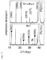
- FIG. 11 is a view showing XRD patterns when changing the number of moles of a paraelectric for 1 mol of a ferroelectric.
- FIG. 12 is a view showing hysteresis characteristics when the number of moles of the paraelectric is in the range of 0.1 ⁇ R ⁇ 1 for 1 mol of the ferroelectric.
- FIG. 13 is a view showing hysteresis characteristics when the number of moles of the paraelectric is in the range of 1 ⁇ R ⁇ 9 for 1 mol of the ferroelectric.
- FIG. 14 is a view showing TEM cross-sectional images of a ferroelectric thin film when changing the pressure of pressure annealing.
- FIG. 15 is a view showing XRD patterns showing a film orientation when using a DLC (diamond-like carbon) buffer layer for the ferroelectric BLSGT thin film of the present invention.
- FIG. 16 is a view showing hysteresis characteristics of a ferroelectric capacitor formed by mixing various catalytic compounds with ferroelectric BIT.
- FIG. 17 is a view showing hysteresis characteristics of a ferroelectric capacitor formed by mixing various catalytic compounds with ferroelectric SBT.
- FIG. 18 is a view showing hysteresis characteristics of a ferroelectric capacitor formed by mixing various catalytic compounds with ferroelectric PZT.
- FIG. 19 is a view showing ferroelectric characteristics of a CaBi 4 Ti 3 Si 0.5 Ge 0.5 O 15 thin film of the present invention.
- FIG. 20 is a view showing ferroelectric characteristics of an Sr 2 (Ta 0.5 , Nb 0.25 , Si 0.125 , Ge 0.125 ) 2 O 7 thin film of the present invention.
- FIG. 21 is a view showing an XRD pattern of a Bi 2 Sr 2 Ca 2 Cu 3 O x +BSO+BGO superconducting thin film of the present invention.
- FIG. 22 is a view showing an MOCVD apparatus used for forming a ferroelectric thin film of the present invention.
- FIG. 23 is a view showing an XRD pattern of a TSO-BGO-BST thin film of the present invention.
- FIG. 24 is a view showing a TEM cross-sectional image of the TSO-BGO-BST thin film of the present invention.
- FIG. 25 is a view showing a relation between a relative dielectric constant and a frequency of the TSO-BGO-BST thin film of the present invention.
- FIG. 26 is a view showing a relation between an applied voltage and the amount of stored charge of the TSO-BGO-BST thin film of the present invention.
- FIG. 27 is a view showing leakage current characteristics of the TSO-BGO-BST thin film of the present invention.
- FIG. 28 is a view showing an LSMCD apparatus using supercritical carrier gas used for forming a ferroelectric thin film of the present invention.
- FIG. 29 is a view showing a relation between a relative dielectric constant and a frequency of the TSO-BGO-BST thin film of the present invention formed by using the LSMCD apparatus using supercritical carrier gas before and after pressure annealing.
- FIG. 30 is a view showing a high-frequency magnetron sputtering apparatus used for forming a ferroelectric thin film of the present invention.
- FIG. 31 is a cross-sectional view showing a BSO-BGO-SBT target of the present invention.
- FIG. 32 is a view showing an XRD pattern of a BSO-BGO-SBT thin film formed by using the high-frequency magnetron sputtering apparatus.
- FIG. 33 is a view showing a TEM cross-sectional image of the BSO-BGO-SBT thin film formed by using the high-frequency magnetron sputtering apparatus.
- FIG. 34 is a view showing hysteresis characteristics of the BSO-BGO-SBT thin film formed by using the high-frequency magnetron sputtering apparatus.
- FIG. 35 is a view showing an XRD pattern of a BSO-BIT thin film formed by using a solid phase method.
- FIG. 36 is a view showing hysteresis characteristics of the BSO-BIT thin film formed by using the solid phase method.
- FIG. 37 is a cross-sectional view schematically showing a ferroelectric memory device.
- FIG. 38 is a cross-sectional view schematically showing an apparatus for forming a raw material body on a substrate by using an LSMCD method.
- FIGS. 39A to 39C are conceptual views schematically showing a manufacturing process for a first multilayer ceramic film.
- FIGS. 40A to 40C are conceptual views schematically showing a manufacturing process for a second multilayer ceramic film.
- FIGS. 41A to 41C are conceptual views schematically showing a manufacturing process for a third multilayer ceramic film.
- FIGS. 42A and 42B are conceptual views schematically showing a manufacturing process for a fourth multilayer ceramic film.
- FIG. 43 is a view showing a TEM image of an oxide ferroelectric thin film of the present invention after presintering.
- FIG. 44 is a view showing EDX composition analysis results at a lower Pt electrode grain boundary and in an Si substrate of an oxide ferroelectric BLST capacitor of the present invention and a conventional ferroelectric BIT capacitor.
- FIG. 45 is a view showing surface morphology of an oxide ferroelectric thin film of the present invention when Ge/Si is 0.1, 5, 10, or 15.
- FIG. 46 is a view showing reduction resistance of an oxide ferroelectric thin film of the present invention when Ge/Si is 0.1, 5, 10, or 15.
- FIG. 47 is a view showing surface morphology of an oxide ferroelectric thin film of the present invention when Sn/Si is 3, 6, or 9.
- FIG. 48 is a view showing reduction resistance of an oxide ferroelectric thin film of the present invention when Sn/Si is 3, 6, or 9.
- FIG. 49 is a view showing reduction resistance of an oxide ferroelectric thin film of the present invention when 1 ⁇ (Ge+Sn)/Si ⁇ 10 and Ge/Sn is 1.2 or 1.5.
- FIG. 50 is a view showing an XRD pattern of a ferroelectric BIT containing Si and Ge of the present invention.
- a first method of manufacturing a ceramic film of the present invention comprises:
- the raw material body includes different types of raw materials in a mixed state
- the different types of raw materials differ from one another in at least one of a crystal growth condition and a crystal growth mechanism in the crystallization of the raw materials.
- the different types of raw materials differ from one another in at least one of the crystal growth condition and the crystal growth mechanism in the crystallization of the raw materials. Specifically, the raw materials are judged to be different depending on whether or not the raw materials differ from one another in at least one of the crystal growth condition and the crystal growth mechanism.
- One of the different types of raw materials is a complex oxide material having an oxygen octahedral structure such as a perovskite material, Bi-layer structured material, superconducting oxide material, and tungsten bronze material, and the other raw material is a paraelectric material such as a layered catalytic substance which includes Si or Si and Ge in the constituent elements.
- crystal growth condition and the crystal growth mechanism in the crystallization of the raw materials examples include a crystallization temperature, crystal nucleus formation temperature, crystal growth temperature, crystal growth rate, crystal nucleus formation rate, size of crystal nuclei, crystallization method, and the like.
- examples include a phenomenon in which the density of initial crystal nuclei is increased by allowing a region in which one of the raw materials is crystallized before the other raw material to occur over the entire film, thereby preventing abnormal growth of crystals to provide good surface morphology.
- the raw material body includes the different types of raw materials.
- the raw material body includes at least two types of raw materials.
- the different types of raw materials differ from one another in at least one of the crystal growth condition and the crystal growth mechanism in the crystallization of the raw materials. Therefore, one of the raw materials can be crystallized before the other raw material and the other raw material can be crystallized in the openings between crystals produced from the above raw material by controlling various conditions, for example. Specifically, the openings between crystals produced from one of the raw materials can be filled with crystals produced from the other raw material. Therefore, surface morphology of the ceramic film can be improved.
- the different types of raw materials may be crystallized at the same time by controlling various conditions.
- the crystallization temperature can be adjusted by causing a metal element of the raw material to be replaced with aother element. This enables the crystallization temperatures of the different types of raw materials to be approximately the same.
- the different types of raw materials can be crystallized at the same time if the crystallization temperatures of the different types of raw materials are approximately the same.
- a second method of manufacturing a ceramic film of the present invention comprises:
- the raw material body includes different types of raw materials in a mixed state
- the different types of raw materials differ from one another in the crystal structure produced from the raw materials. Specifically, the raw materials are judged to be different when the raw materials differ from one another in the crystal structure of the crystals obtained from the raw materials.
- crystals obtained from the raw materials are expressed as (Bi 2 O 2 ) 2+ (A m ⁇ 1 B m O 3m+1 ) 2 ⁇ , crystals having a different crystal structure have different values for m, different elements for A and B, and the like.
- crystals obtained from the raw materials are expressed as (Bi 2 O 2 ) 2+ (A m ⁇ 1 B m O 3m+1 ) 2 ⁇
- crystals having a different crystal structure have either Si or Si and Ge for B.
- the different types of raw materials differ from one another in the crystal structures produced from the raw materials. If the raw materials differ from one another in the crystal structure of the crystals obtained from the raw materials, the raw materials differ from one another in the crystal growth condition and the crystal growth mechanism of the raw materials. Therefore, effects the same as in the first method of manufacturing a ceramic film of the present invention can be obtained.
- a third method of manufacturing a ceramic film of the present invention comprises:
- the raw material body includes different types of raw materials in a mixed state
- the different types of raw materials are individually crystallized at least at an initial stage of crystallization.
- the different types of raw materials are individually crystallized at least at an initial stage of crystallization. Therefore, crystals produced from one of the raw materials can be grown in the openings between crystals produced from the other raw material. As a result, occurrence of openings between the crystals can be prevented, whereby the surface morphology is improved.
- the first to third methods of manufacturing a ceramic film of the present invention may have any of the following features.
- the ceramic film may be a ferroelectric or a high dielectric.
- the ceramic film may be a paraelectric.
- the ceramic film may include a ferroelectric and a paraelectric in a mixed state.
- At least two of the different types of raw materials may differ from each other in crystallization temperature in the crystallization of the raw materials.
- At least two of the different types of raw materials may differ from each other in crystal nucleus formation temperature in the crystallization of the raw materials.
- At least two of the different types of raw materials may differ from each other in crystal growth temperature in the crystallization of the raw materials.
- At least two of the different types of raw materials may differ from each other in crystal growth rate in the crystallization of the raw materials.
- At least two of the different types of raw materials may differ from each other in crystal nucleus formation rate in the crystallization of the raw materials.
- At least two of the different types of raw materials may differ from each other in the size of crystal nuclei in the crystallization of the raw materials.
- At least two of the different types of raw materials may differ from each other in crystallization method in the crystallization of the raw materials.
- One of the raw materials crystallized first may have a catalytic effect for the other raw material crystallized later.
- the different types of raw materials may be compound-crystallized at the same time.
- raw materials which produce a ceramic having a different crystal structure When crystallizing the different types of raw materials at the same time, it is preferable to use raw materials which produce a ceramic having a different crystal structure. This enables the crystal growth conditions and the crystal growth mechanism during crystallization of the raw materials to be changed at the same time.
- One of the different types of raw materials may be a complex oxide material having an oxygen octahedral structure such as a perovskite and bismuth-layer structured oxide material shown by ABO 3 or (Bi 2 O 2 ) 2+ (A m ⁇ 1 B m O 3m+1 ) 2 ⁇ (wherein A represents at least one element selected from the group consisting of Li, Na, K, Rb, Pb, Ca, Sr, Ba, Bi, La, and Hf, B represents at least one element selected from the group consisting of Ru, Fe, Ti, Zr, Nb, Ta, V, W, and Mo, and m is a natural number of 5 or less), a superconducting oxide material shown by LanBa 2 Cu 3 O 7 , Trm 2 Ba 2 Ca n ⁇ 1 Cu n O 2n+4 , or TrmBa 2 Ca n ⁇ 1 Cu n O 2n+3 (wherein Lan represents at least one ion selected from the group consisting of Y, La, Ce,
- the raw material body may be formed on a substrate by using a liquid source misted chemical deposition (LSMCD) method.
- LSMCD liquid source misted chemical deposition
- the raw material body is provided to the substrate in the form of a mist by ultrasonic waves. This improves mixing conditions for the different types of raw materials. Therefore, a ceramic film having microcrystals can be obtained.
- the raw material body may be formed on a substrate by separately providing the different types of raw materials.
- the raw material body may be formed on a substrate by providing the different types of raw materials at the same time.
- the raw material body may be formed on a substrate by spin coating or dipping.
- the raw material body may be formed on a substrate by a metal-organic chemical vapor deposition (MOCVD) method.
- MOCVD metal-organic chemical vapor deposition
- the raw material body may be formed on a substrate by sputtering or laser ablation.
- the raw material body may be formed on a substrate by a solid phase method.
- the raw materials may be at least one of a sol-gel raw material and an MOD raw material.
- the raw material body may include a sol-gel raw material and an MOD raw material.
- the sol-gel raw material may be polycondensed by hydrolysis.
- the sol-gel raw material may be complex polymerized by hydrolysis.
- the sol-gel raw material may have a crystal structure similar to the crystal structure of crystals obtained by crystallizing the raw material. This enables the sol-gel raw material to be easily crystallized.
- the MOD raw material may be a polynuclear complex raw material.
- the raw material body may include different types of sol-gel raw materials, and the different types of sol-gel raw materials may differ from one another in the degree of polycondensation or metal element composition.
- the raw material body may include different types of sol-gel raw materials, and the different types of sol-gel raw materials may not be mixed at an atomic level or a molecular level.
- the term “mixed at an atomic level” means that atoms which make up the raw materials are mixed, for example. Specifically, the raw materials are preferably mixed in a state in which individual molecules or aggregates are maintained. If the raw materials are not mixed at an atomic level or a molecular level, the effects of the present invention can be obtained reliably. Moreover, characteristics of the ceramic film can be further improved.
- the sol-gel raw material is in a state in which a long polycondensed organic metal network is dispersed in a solvent. This aims at bringing constituent elements of an objective oxide close to one another in advance.
- the MOD raw material is in a state in which the constituent elements of an objective oxide are dispersed without being bonded to one another.
- the feature in which the raw material body of the present invention includes the different types of sol-gel raw materials, and the different types of sol-gel raw materials are not mixed at an atomic level or a molecular level means as follows.
- the constituent elements of the sol-gel raw material for a ferroelectric form a network.
- the constituent elements of the sol-gel raw material for a paraelectric also form a network. However, these networks are not polycondensed and have a relation similar to that of the constituent elements in the MOD raw material. Specifically, these networks are not mixed at an atomic level or a molecular level. This enables each of the objective oxides to be formed separately.
- a fourth method of manufacturing a ceramic film of the present invention comprises:
- the raw material body is crystallized so that a plurality of phases is formed.
- the ceramic film may have any of the following features.
- the ceramic film may be a ferroelectric or a high dielectric.
- the ceramic film may be a paraelectric.
- the ceramic film may include a ferroelectric and a paraelectric in a mixed state.
- a fifth method of manufacturing a ceramic film of the present invention comprises:
- first raw material liquid and the second raw material liquid are different types of liquids
- the first raw material liquid is a raw material liquid for producing a ferroelectric including a perovskite material, Bi-layer structured material, superconducting oxide material, and tungsten bronze material, and
- the second raw material liquid is a raw material liquid for producing a layered catalytic oxide in which Si or Si and Ge are provided in the B site.
- a ferroelectric film having specific characteristics at a low temperature can be formed by forming a ceramic film using the ceramic raw material liquid of the present invention.
- a ceramic film obtained by using the ceramic raw material liquid of the present invention has excellent surface morphology.
- a ferroelectric ceramic film can be formed by crystallizing the raw material body.
- a ceramic film including a ferroelectric and a paraelectric in a mixed state can be formed by crystallizing the raw material body.
- a ferroelectric ceramic film including a ferroelectric and a paraelectric in a mixed state can be formed by crystallizing the raw material body.
- a ferroelectric ceramic film orientated in an optional direction can be formed by providing DLC for determining the growth direction of the fifth ceramic film of the present invention at the interface with the substrate when crystallizing the ceramic film.
- the first raw material liquid may be a solution in which a metal compound or a metal-inorganic compound of a metal element for the ferroelectric is dissolved in a solvent
- the second raw material liquid may be a solution in which a metal compound or a metal-inorganic compound of a metal element for the layered catalytic oxide is dissolved in a solvent.
- a sixth method of manufacturing a ceramic film of the present invention comprises:
- an uppermost raw material layer in the raw material body layer has a crystallization temperature lower than the crystallization temperature of a lower raw material layer which is in contact with the uppermost raw material layer.
- crystals produced from the uppermost raw material layer function as a seed layer during crystallization of the lower raw material layer. Moreover, since crystals obtained from the uppermost raw material layer have no layered structure, the surface morphology of the ceramic film can be improved.
- the lower raw material layer which is in contact with the uppermost raw material layer may be formed on a substrate with a first raw material layer interposed therebetween, and the first raw material layer may have a crystallization temperature lower than the crystallization temperature of the lower raw material layer which is in contact with the uppermost raw material layer. Therefore, crystals produced from the first raw material layer function as a seed layer during crystallization of the lower raw material layer which is in contact with the uppermost raw material layer.
- a seventh method of manufacturing a ceramic film of the present invention comprises:
- a step of forming a raw material body layer which includes a raw material laminate in which a first raw material layer, a second raw material layer, and a third raw material layer are layered in that order, and
- the second raw material layer has a crystallization temperature lower than crystallization temperatures of the first and third raw material layers.
- crystals produced from the second raw material layer function as a stopper for preventing the growth of crystals in the first raw material layer and the third raw material layer.
- the grain size of the crystals produced from the first raw material layer and the third raw material layer can be reduced.
- a fourth raw material layer may be further layered on the third raw material layer, and the fourth raw material layer may have a crystallization temperature lower than the crystallization temperature of the third raw material layer.
- crystals produced from the fourth raw material layer function as a seed layer during crystallization of the third raw material layer.
- An eighth method of manufacturing a ceramic film of the present invention comprises:
- an uppermost raw material layer in the raw material body layer has a crystallization temperature higher than the crystallization temperature of a lower raw material layer which is in contact with the uppermost raw material layer.
- crystals produced from the uppermost raw material layer can be formed to cover crystals produced from the lower raw material layer.
- the crystals obtained from the uppermost raw material layer in the raw material body layer preferably have no layered structure. This enables the surface morphology of the ceramic film to be improved.
- the step of forming a ceramic film by crystallizing the raw material body may be performed two or more times.
- a first ceramic film of the present invention is obtained by a method of manufacturing a ceramic film of the present invention.
- a second ceramic film of the present invention comprises:
- the second crystal layer has a melting point lower than the melting point of the first crystal layer
- crystals in the second crystal layer do not have a layered structure.
- a region in which a constituent metal element of the first crystal layer and a constituent metal element of the second crystal layer are mixed may be present near the interface between the first crystal layer and the second crystal layer.
- the first crystal layer may be formed on a substrate with a third crystal layer interposed therebetween, and the third crystal layer may have a melting point lower than the melting point of the first crystal layer.
- a third ceramic film of the present invention comprises:
- the second crystal layer has a melting point lower than melting points of the first crystal layer and the third crystal layer.
- a region in which a constituent metal element of the first crystal layer and a constituent metal element of the second crystal layer are mixed may be present near the interface between the first crystal layer and the second crystal layer, and a region in which a constituent metal element of the second crystal layer and a constituent metal element of the third crystal layer are mixed may be present near the interface between the second crystal layer and the third crystal layer.
- a fourth crystal layer may be formed on the third crystal layer, the fourth crystal layer may have a melting point lower than the melting point of the third crystal layer, and a region in which a constituent metal element of the third crystal layer and a constituent metal element of the fourth crystal layer are mixed may be present near the interface between the third crystal layer and the fourth crystal layer.
- a fourth ceramic film of the present invention comprises:
- the second crystal layer has a melting point higher than the melting point of the first crystal layer
- crystals in the second crystal layer do not have a layered structure.
- a region in which a constituent metal element of the first crystal layer and a constituent metal element of the second crystal layer are mixed may be present near the interface between the first crystal layer and the second crystal layer.
- a semiconductor device of the present invention comprises a capacitor including a ceramic film of the present invention.
- An element of the present invention comprises the ceramic film of the present invention.
- the present invention further provides a ferroelectric capacitor and a method of manufacturing a ceramic film given below.
- a ferroelectric capacitor of the present invention comprises:
- a lower electrode a ceramic film which includes first crystals and second crystals and is formed on the lower electrode, and an upper electrode formed on the ceramic film,
- the first crystals include a perovskite material, Bi-layer structured material, superconducting oxide material, and tungsten bronze structure,
- the second crystals are a paraelectric oxide having an oxygen tetrahedral structure consisting of SiO 2 or a mixture of SiO 2 and GeO 2 in the structure, and
- first crystals are intermittently formed in the planar direction of the ceramic film, and the second crystals are formed so as to be interposed between the first crystals.
- the ceramic film which makes up the ferroelectric capacitor may be formed by a first method given below.
- the first method comprises:
- first raw material liquid and the second raw material liquid are different types of liquids
- the first raw material liquid is a raw material liquid for producing a perovskite material, Bi-layer structured material, superconducting oxide material, and ferroelectric having a tungsten bronze structure
- the second raw material liquid is a raw material liquid for producing a layered catalytic oxide in which Si or Si and Ge are provided in the B site
- first crystals produced from the first raw material liquid are intermittently formed in the planar direction of the ceramic film, and second crystals produced from the second raw material liquid are formed so as to be interposed between the first crystals by depositing the ceramic film in a state in which the first raw material liquid and the second raw material liquid are phase separated.
- the ceramic film which makes up the ferroelectric capacitor may be formed by a second method given below.
- the second method comprises:
- first raw material liquid and the second raw material liquid are different types of liquids
- the first raw material liquid is a raw material liquid for producing a perovskite material, Bi-layer structured material, superconducting oxide material, and ferroelectric including a tungsten bronze structure
- the second raw material liquid is a raw material liquid for producing a layered catalytic oxide in which Si or Si and Ge are provided in the B site
- first crystals produced from the first raw material liquid are intermittently formed in the planar direction of the ceramic film, and second crystals produced from the second raw material liquid are formed so as to be interposed between the first crystals by forming a mist of the first raw material liquid so as to be dispersed on a substrate, and forming a film of the second raw material liquid on the substrate.
- the second method as the method for forming the film of the second raw material liquid on the substrate on which the mist produced from the first raw material liquid is dispersed, a method of forming the film in a state in which the second raw material liquid is misted, or a method of forming the film of the second raw material liquid by spin coating may be used. These methods also apply to a second method described later.
- the first and second methods may have the following features. These features also applied to first and second methods described later.
- One of the solvents included in the first raw material liquid and the second raw material liquid may be soluble in water, and the other solvent may be insoluble in water.
- the molar ratio of the ferroelectric produced from the first raw material liquid to the ABO-type oxide produced from the second raw material liquid may be from 100:20 to 100:100.
- the first raw material liquid may be a solution in which a metal compound or a metal inorganic compound of a metal element for the ferroelectric is dissolved in a solvent, and
- the second raw material liquid may be a solution in which a metal compound or a metal inorganic compound of a metal element for the layered catalytic oxide in which Si or Si and Ge are provided in the B site is dissolved in a solvent.
- a ferroelectric capacitor of the present invention comprises:
- a lower electrode a ceramic film which includes first crystals and second crystals and is formed on the lower electrode, and an upper electrode formed on the ceramic film,
- the first crystals include a perovskite material, Bi-layer structured material, superconducting oxide material, and tungsten bronze structure,
- the second crystals are a layered catalytic oxide in which Si, or Si and Ge are provided in the B site, and
- first crystals are intermittently formed in the planar direction of the ceramic film, and the second crystals are formed so as to be interposed between the first crystals.
- the ceramic which makes up the ferroelectric capacitor may be formed by a method similar to the above first and second methods.
- a first method comprises:
- the third raw material liquid is a raw material liquid for producing a perovskite material, Bi-layer structured material, superconducting oxide material, and tungsten bronze type ferroelectric,
- the fourth raw material liquid is a raw material liquid for producing a layered catalytic oxide in which Si or Si and Ge are provided in the B site,
- third crystals produced from the third raw material liquid are intermittently formed in the planar direction of the ceramic film, and fourth crystals produced from the fourth raw material liquid are formed so as to be interposed between the third crystals by depositing the ceramic film in a state in which the third raw material liquid and the fourth raw material liquid are phase separated.
- a second method comprises:
- the third raw material liquid is a raw material liquid for producing a perovskite material, Bi-layer structured material, superconducting oxide material, and tungsten bronze type ferroelectric,
- the fourth raw material liquid is a raw material liquid for producing a layered catalytic oxide in which Si or Si and Ge are provided in the B site,
- third crystals produced from the third raw material liquid are intermittently formed in the planar direction of the ceramic film, and fourth crystals produced from the fourth raw material liquid are formed so as to be interposed between the third crystals by forming a mist of the third raw material liquid so as to be dispersed on a substrate, and forming a film of the fourth raw material liquid on the substrate.
- the method of forming the film of the fourth raw material liquid on the substrate on which the mist produced from the third raw material liquid is dispersed a method of forming the film in a state in which the fourth raw material liquid is misted, or a method of forming the film of the fourth raw material liquid by spin coating may be used.
- the first and second methods may have the following features.
- One of the solvents included in the third raw material liquid and the fourth raw material liquid may be soluble in water, and the other solvent may be insoluble in water.
- the molar ratio of the ferroelectric produced from the third raw material liquid to the ABO-type oxide produced from the fourth raw material liquid may be from 100:20 to 100:100.
- the third raw material liquid may be a solution in which a metal compound or a metal-inorganic compound of a metal element for the ferroelectric is dissolved in a solvent
- the fourth raw material liquid may be a solution in which a metal compound or a metal-inorganic compound of a metal element for the layered catalytic oxide is dissolved in a solvent.
- a ferroelectric capacitor of the present invention comprises:
- a lower electrode a ceramic film which includes first crystals and second crystals and is formed on the lower electrode, and an upper electrode formed on the ceramic film,
- first crystals are intermittently formed in the planar direction of the ceramic film, and the second crystals are formed so as to be interposed between the first crystals.
- a first method for forming the ceramic film which makes up the ferroelectric capacitor comprises:
- first raw material liquid and the second raw material liquid are different types of liquids
- the first raw material liquid is a raw material liquid for producing a ferroelectric
- the second raw material liquid is a raw material liquid for producing a layered catalytic oxide
- first crystals produced from the first raw material liquid are intermittently formed in the planar direction of the ceramic film, and second crystals produced from the second raw material liquid are formed so as to be interposed between the first crystals by depositing the ceramic film in a state in which the first raw material liquid and the second raw material liquid are phase separated.
- a second method for forming the ceramic film which makes up the ferroelectric capacitor comprises:
- first raw material liquid and the second raw material liquid are different types of liquids
- the first raw material liquid is a raw material liquid for producing a ferroelectric
- the second raw material liquid is a raw material liquid for producing a layered catalytic oxide in which Si or Si and Ge are provided in the B site
- first crystals produced from the first raw material liquid are intermittently formed in the planar direction of the ceramic film, and second crystals produced from the second raw material liquid are formed so as to be interposed between the first crystals by forming a mist of the first raw material liquid so as to be dispersed on a substrate, and forming a film of the second raw material liquid on the substrate.
- the manufacturing methods may be applied not only to the case of the above-described ferroelectric having a Bi-type layered perovskite structure or a PZT-type perovskite structure, but also to the case where the first raw material liquid is a raw material liquid for producing a perovskite material, Bi-layer structured material, superconducting oxide material, and tungsten bronze type ferroelectric,
- the fourth raw material liquid is a raw material liquid for producing a layered catalytic oxide in which Si or Si and Ge are provided in the B site
- the second raw material liquid is a raw material liquid for producing a layered catalytic oxide in which Si or Si and Ge are provided in the B site.
- the first crystals produced from the first or third raw material liquid are intermittently formed in the planar direction of the ceramic film, and the second crystals produced from the second or fourth raw material liquid are formed so as to be interposed between the first crystals.
- occurrence of domains in the direction at an angle of 90° with respect to the direction of the thickness of the ferroelectric film of the ferroelectric capacitor formed by the upper and lower electrodes and the ferroelectric (generally called 90° domains) can be prevented.
- squareness of the hysteresis characteristics of the ferroelectric capacitor can be improved.
- a ceramic of the present invention is a complex oxide having an oxygen octahedral structure, and comprises Si and Ge in the oxygen octahedral structure.
- the ceramic of the present invention may be referred to as a ceramic in which a paraelectric including Si and Ge is dissolved in a complex oxide having an oxygen octahedral structure.
- Si and Ge included in such an oxygen octahedral structure have a coordination number of six.
- the ceramic of the present invention is obtained by replacing metal cations (B site ions) positioned in the oxygen octahedral structure of the complex oxide with an Si ion and a Ge ion.
- a (Bi, La) 4 (Ti, Si, Ge) 3 O 12 ferroelectric of the present invention is obtained by replacing the B site ions with Si 4+ and Ge 4+ .
- Such a (Bi, La) 4 (Ti, Si, Ge) 3 O 12 structure cannot be easily known from the analogy to Bi 4 Ti 3 O 12 .
- Si 4+ and Ge 4+ have strong covalent bonding properties and are not metal elements.
- Formation of the ceramic of the present invention is remarkably facilitated by replacing part of the B sites of the oxygen octahedron with Si and Ge. Since the ionic radius of Ge is larger than that of Si and close to the lattice spacing of the B site, Ge has remarkably high capability of replacing the B site of the oxygen octahedron in comparison with Si. Since the entire lattice of the oxygen octahedron shrinks or is distorted when Ge enters the B site of the oxygen octahedron, Si easily replaces the B site. In this case, it is important to use Si and Ge at the same time. This is because the introduction of covalent bonding properties into the oxygen octahedron is insufficient only by using Ge, whereby the catalytic function of the paraelectric is insufficient.
- the molar ratio of Ge to Si in the ceramic of the present invention is preferably 0 ⁇ Ge/Si ⁇ 10, and still more preferably 0 ⁇ Ge/Si ⁇ 1.
- the ratio of Ge to Si is within the specific range, good surface morphology, crystallinity, and interface can be obtained.
- the ratio is 0 ⁇ Ge/Si ⁇ 1, covalent bonding properties are increased due to a high percentage of Si having a small ionic radius, whereby the reduction resistance is remarkably improved.
- the ratio is 0 ⁇ Ge/Si ⁇ 10, since Ge is the same group element as Si and has a large ionic radius for one period, Ge is easily added to the oxygen octahedral structure, whereby the thin film of the present invention can be easily formed.
- the surface morphology deteriorates as the ratio of Ge to Si is increased, as shown in FIG. 45 .
- the surface morphology becomes rough, but also the reduction resistance significantly deteriorates, as shown in FIG. 46 .
- the thin film of the present invention can be further facilitated by using Sn instead of Ge, since Sn is easily added to the oxygen octahedral structure for a further increase in the ionic radius.
- the ratio of Sn to Si is 0 ⁇ Sn/Si ⁇ 9. If the ratio is 9 ⁇ Sn/Si, the surface morphology significantly deteriorates as shown in FIG. 47 . Moreover, reduction resistance significantly deteriorates when subjected to a heat treatment for 10 minutes in a 3% H 2 atmosphere, as shown in FIG. 48 .
- the complex oxide having the oxygen octahedral structure may be at least one oxide selected from a perovskite, bismuth-layer structured oxide, superconducting oxide, and tungsten bronze structured oxide, and the paraelectric may be a layered catalytic substance which includes Si and Ge in the constituent elements.
- the ceramic of the present invention may be a complex oxide having an oxygen octahedral structure, and comprise a ferroelectric layer which includes Si or Si and Ge, and a paraelectric layer having an oxygen tetrahedral structure which includes Si or Si and Ge in the constituent elements in the oxygen octahedral structure, wherein at least one of the ferroelectric layer and the paraelectric layer may have a column-shaped structure extending in the direction of the film thickness.
- the layer having the column-shaped structure may have a diameter of 1 to 50 nm.
- the present inventors have found that, when the number of moles of the layered catalytic compound is relatively larger than that of the complex oxide having an oxygen octahedron, an excess layered catalytic compound is separated from the complex oxide having an oxygen octahedron in the direction of the film thickness. Therefore, characteristics such as ferroelectric characteristics can optionally be set by controlling the amount of the layered catalytic compound to be added.
- the mixing ratio of the complex oxide material to the paraelectric material is set taking into consideration the above characteristics such as ferroelectric characteristics. For example, if the molar ratio of the complex oxide material to the paraelectric material is 1 or more, characteristics can be controlled by optionally changing the material characteristics of the complex oxide material such as a remanent polarization in the case of using a ferroelectric material. If the molar ratio of the complex oxide material to the paraelectric material is less than 1, the surface morphology, crystallinity, and reduction resistance can be improved without changing the material characteristics of the complex oxide material such as a remanent polarization in the case of using a ferroelectric material.
- second crystals are disposed to surround first crystals (ferroelectric, for example).
- first crystals ferroelectric, for example.
- a method of manufacturing a ceramic according to the present invention comprises forming a film which includes a complex oxide material having an oxygen octahedral structure and a paraelectric material having a catalytic effect for the complex oxide material in a mixed state, and subjecting the film to a heat treatment, wherein the paraelectric material is a layered catalytic substance which includes Si in the constituent elements or a layered catalytic substance which includes Si and Ge in the constituent elements.
- covalent bonding properties are increased over the entire crystal lattice by introducing Si and Ge into the oxygen octahedron of various types of complex oxide materials having strong ionic bonding properties such as a perovskite material, bismuth-layer structured material, superconducting oxide material, and tungsten bronze material, whereby resistance to reduction due to hydrogen or the like is increased.
- a metal element such as V or W for which replacement in the crystal lattice is difficult using a coating method such as spin coating, can be easily replaced.
- the heat treatment may include sintering and post-annealing, wherein at least the post-annealing may be performed in a pressurized atmosphere containing at least either oxygen or ozone (hereinafter called “oxygen atmosphere”).
- oxygen atmosphere containing at least either oxygen or ozone
- the post-annealing is preferably performed in a pressurized state such as at 2 atm. or more, and still more preferably at 2 to 9.9 atm.
- the post-annealing may be performed after forming an electrode on the film in which the complex oxide material and the paraelectric material are present in a mixed state.
- the characteristics of the ceramic can be further stabilized and improved by performing post-annealing in such a pressurized oxygen atmosphere.
- Oxygen deficiency shift of XRD peak to higher angle side
- Oxygen deficiency shift of XRD peak to higher angle side
- crystal growth characteristics and leakage current characteristics can be improved.
- good ferroelectric characteristics can be stably obtained.
- the oxide thin film of the present invention is formed of a mixture of fine crystal particles. Crystal growth is promoted by performing pressure annealing in oxygen at a comparatively low temperature, for example, annealing at 500° C. and 9.9 atm. in a 100% oxygen atmosphere, whereby the structure of the thin film is close to a single crystal structure. Specifically, crystals show behavior similar to epitaxial growth by pressure annealing in the oxygen atmosphere. It is known that oxygen deficiency is improved by performing pressure annealing in a conventional complex oxide material. However, behavior similar to epitaxial growth is peculiar to the complex oxide material of the present invention which includes Si and Ge in the oxygen octahedron.
- the heat treatment in the pressurized oxygen atmosphere has a sufficient effect after crystallization. However, it is more effective to perform the heat treatment after providing an upper electrode taking into consideration the interface state between the film and the upper electrode.
- processing can be performed in an amorphous state which enables easy processing and thermal damage to the element can be minimized by performing crystallization in the pressurized oxygen atmosphere and formation of the upper electrode at the same time.
- the paraelectric material a compound having an effect of lowering the crystallization temperature of the complex oxide material, specifically, a layered catalytic compound having a crystallization temperature lower than that of the ferroelectric is used.
- the paraelectric material preferably includes Si or Si and Ge having a coordination number of four, and has an oxygen tetrahedral structure. Since the layered catalytic compound which includes Si and Ge in the constituent elements has a low crystallization temperature and low density, the layered catalytic compound has high catalytic action. Moreover, the layered catalytic compound has good lattice matching with many oxide materials having an oxygen octahedron. Therefore, the layered catalytic compound which includes Si and Ge is first crystallized in the film, and the complex oxide material is crystallized on the surface of the layered catalytic compound by effectively utilizing the catalytic action of the layered catalytic compound.
- activation energy required for the crystallization of the complex oxide is reduced by using the layered catalytic compound, whereby the crystallization temperature is lowered.
- the applied energy can be effective utilized for compensation for oxygen deficiency and crystal growth.
- the layered catalytic compound of the present invention Since the constituent elements of the layered catalytic compound of the present invention replace the A and B sites of the oxygen octahedron therewith when the elements have finished the function as a catalyst, the layered catalytic compound does not essentially allow the layered catalytic compound structure to remain. As a result, since the layered catalytic compound is not formed to separate the film in the direction of the thickness, a decrease in ferroelectric characteristics and electrical characteristics can be prevented.
- a sol-gel raw material may be used for at least one of the complex oxide material and the paraelectric material. At least one of the complex oxide material and the paraelectric material may be formed by using a complex polymerization method.
- the film in which the complex oxide material and the paraelectric material are present in a mixed state is formed by any of a solid phase method, coating method, LSMCD method, MOCVD method, and sputtering method.
- a coating method spin coating or the like may be used.
- At least one of the complex oxide material and the paraelectric material may be provided on a substrate by using a supercritical fluid.
- the complex oxide material having an oxygen octahedral structure is at least one material selected from a perovskite material, bismuth-layer structured oxide, superconducting oxide, and tungsten bronze structured oxide, and
- the paraelectric material is a layered catalytic compound which includes Si in the constituent elements or a layered catalytic compound which includes Si and Ge in the constituent elements.
- the complex oxide material having an oxygen octahedral structure may be at least one of a perovskite and bismuth layer structured oxide shown by ABO 3 or (Bi 2 O 2 ) 2+ (A m ⁇ 1 B m O 3m+1 ) 2 ⁇ (wherein A represents at least one element selected from the group consisting of Li, Na, K, Rb, Pb, Ca, Sr, Ba, Bi, La, and Hf, B represents at least one element selected from the group consisting of Ru, Fe, Ti, Zr, Nb, Ta, V, W, and Mo, and m is a natural number of 5 or less), a superconducting oxide shown by LanBa 2 Cu 3 O 7 , Trm 2 Ba 2 Ca n ⁇ 1 Cu n O 2n+4 , or TrmBa 2 Ca n ⁇ 1 Cu n O 2n+3 (wherein Lan represents at least one element selected from the group consisting of Y, La, Ce, Pr, Nd, Pm, Sm, Eu, G
- the paraelectric material may be a paraelectric material which includes at least one compound selected from the group consisting of CaO, BaO, PbO, ZnO, MgO, B 2 O 3 , Al 2 O 3 , Y 2 O 3 , La 2 O 3 , Cr 2 O 3 , Bi 2 O 3 , Ga 2 O 3 , ZrO 2 , TiO 2 , HfO 2 , NbO 2 , MoO 3 , WO 3 , and V 2 O 5 , and SiO 2 or SiO 2 and GeO 2 .
- the paraelectric material may be a layered compound having an oxygen tetrahedral structure which includes at least one compound selected from the group consisting of CaSiO 3 , BaSiO 3 , PbSiO 3 , ZnSiO 3 , MgSiO 3 , B 2 SiO 5 , Al 2 SiO 5 , Y 2 SiO 5 , La 2 SiO 5 , Cr 2 SiO 5 , Bi 2 SiO 5 , Ga 2 SiO 5 , ZrSiO 4 , TiSiO 4 , HfSiO 4 , NbSiO 4 , MoSiO 5 , WSiO 5 , and V 2 SiO 7 , or a layered compound having an oxygen tetrahedral structure which includes at least one compound selected from the group consisting of CaSiO 3 , BaSiO 3 , PbSiO 3 , ZnSiO 3 , MgSiO 3 , B 2 SiO 5 , Al 2 Si
- An oxide material in which the B site of the perovskite, bismuth-layer structured oxide, superconducting oxide, or tungsten bronze structured compound which makes up the complex oxide material is replaced with Si or Si and Ge may be formed in advance by using a complex polymerization method.
- a DLC (diamond-like carbon) film may be formed on a substrate, and the film in which the complex oxide material and the paraelectric material are present in a mixed state may be formed on the DLC film.
- a dielectric capacitor according to the present invention comprises a lower electrode, a film of the ceramic of the present invention which is formed on the lower electrode, and an upper electrode formed on the ceramic film.
- At least part of the ceramic may have a column-shaped structure which is continuous between the upper electrode and the lower electrode.
- the diameter of the column-shaped structure may be 1 to 50 nm.
- a semiconductor substrate such as an element semiconductor such as silicon and germanium and a compound semiconductor such as GaAs and ZnSe, a metal substrate such as Pt, an insulating substrate such as a sapphire substrate, an MgO substrate, SrTiO 3 , BaTiO 3 , and a glass substrate, and the like can be given.
- a silicon substrate is preferable, and a single crystal silicon substrate is still more preferable.
- An electrode may be formed on the substrate.
- the electrode may be formed by using a metal such as Pt, Ir, Au, Al, or Ru, an oxide conductor such as IrO 2 and RuO 2 , a nitride conductor such as TiN and TaN, or the like.
- the thickness of the electrode is about 100 to 200 nm, for example.
- Intermediate layers such as an insulating layer and an adhesive layer may be formed between the electrode and the substrate.
- the insulating layer may be formed using SiO 2 , Si 3 N 4 , or the like.
- the material for the adhesive layer insofar as the adhesive layer can secure bonding strength between the substrate and the electrode or between the insulating layer and the electrode.
- a high-melting-point metal such as tantalum or titanium may be used.
- These intermediate layers may be formed by using various methods such as a thermal oxidation method, CVD method, sputtering method, vacuum deposition method, or MOCVD method.
- the ceramic of the present invention may be applied to a dielectric capacitor, a semiconductor device, and various types of other devices.
- FIG. 1 is a cross-sectional view showing a high-dielectric/ferroelectric capacitor (hereinafter called “ferroelectric capacitor” or “high-dielectric capacitor”) which is manufactured by the manufacturing method of the present invention and is used for evaluation of electrical characteristics as described later.
- a silicon thermal oxide film 2 is formed on the surface of an n-type silicon substrate 1 as an interlayer dielectric.
- FIG. 37 is a cross-sectional view schematically showing a ferroelectric memory device to which the dielectric capacitor of the present invention is applied.
- a ferroelectric memory device 5000 includes a CMOS region R 1 and a capacitor region R 2 formed on the CMOS region R 1 .
- the CMOS region R 1 includes a semiconductor substrate 1 , an element isolation region 2 and a MOS transistor 3 which are formed on the semiconductor substrate 1 , and an interlayer dielectric 4 .
- the capacitor region R 2 includes a capacitor C 100 consisting of a lower electrode 5 , a ferroelectric film 6 , and an upper electrode 7 , an interconnect layer 8 a connected with the lower electrode 5 , an interconnect layer 8 b connected with the upper electrode 7 , and an insulating layer 9 .
- the ferroelectric film 6 of the capacitor C 100 is formed by using the method of manufacturing the ceramic of the present invention.
- An impurity diffusion layer 3 a of the MOS transistor 3 and the lower electrode 5 which makes up the capacitor are connected by a contact layer 11 formed of polysilicon or tungsten.
- FIG. 39 is a cross-sectional view schematically showing the manufacturing process for the first multilayer ceramic film.
- a main liquid layer 312 for producing a ferroelectric is formed on the substrate 10 by using a coating method.
- the material for the main liquid layer 312 the first raw material liquid in the second embodiment and the third raw material liquid in the third embodiment can be given.
- a secondary liquid layer 322 for producing either a ferroelectric or a paraelectric is formed on the main liquid layer 312 .
- a material having a crystallization temperature lower than that of the material for the main liquid layer 312 is selected.
- a material which produces an oxide having no layered structure after crystallization is selected as the material for the secondary liquid layer 322 .
- the material for the secondary liquid layer 322 differs depending upon the material for the main liquid layer 312 .
- the material for the secondary liquid layer 322 a is a BiGeO-type material, BiSiO-type material, or SrGeO-type material, for example.
- the main liquid layer 312 and the secondary liquid layer 322 are crystallized by performing a heat treatment, whereby a ceramic film 300 consisting of a main crystal layer 310 and a secondary crystal layer 320 is formed.
- a material having a crystallization temperature lower than that of the main liquid layer 312 is selected as the material for the secondary liquid layer 322 . Therefore, the secondary liquid layer 322 is crystallized before the main liquid layer 312 at an initial stage of crystallization, as shown in FIG. 39B . As a result, crystals produced in the secondary liquid layer 322 function as seeds during the crystallization of the main liquid layer 312 . Therefore, crystallization of the main liquid layer 312 proceeds in the direction from the secondary liquid layer 322 and from the substrate 10 . This enables the grain size of crystals produced in the main liquid layer 312 to be decreased.
- the material for the secondary liquid layer 322 As the material for the secondary liquid layer 322 , a material which produces an oxide having no layered structure after crystallization is selected. Therefore, crystals are isotropically grown in the secondary liquid layer 322 . As a result, a secondary crystal layer 320 with a flat surface is formed, whereby the surface morphology of the ceramic film 300 can be improved.
- the ceramic film 300 consisting of the main crystal layer 310 and secondary crystal layers 320 and 330 may be formed by allowing a secondary liquid layer 332 to be interposed between the substrate 10 and the main liquid layer 312 , as shown in FIG. 40A .
- FIG. 41 is a cross-sectional view schematically showing the manufacturing process for the second multilayer ceramic film.
- the example of the manufacture of the second multilayer ceramic film differs from the example of the manufacture of the first multilayer ceramic film in that a secondary liquid layer 422 is interposed between main liquid layers 412 and 432 .
- main liquid layer 412 , secondary liquid layer 422 , main liquid layer 432 , and secondary liquid layer 442 are layered on the substrate 10 in that order.
- a ceramic film 400 consisting of main crystal layers 410 and 430 and secondary crystal layers 420 and 440 are formed by crystallizing these layers.
- a material having a crystallization temperature lower than those of the main liquid layers 412 and 432 is selected in the same manner as in the example of the manufacture of the first multilayer ceramic film.
- Crystals produced in the secondary liquid layer 422 function as a stopper for preventing crystal growth in the main liquid layers 412 and 432 by allowing the secondary liquid layer 422 to be interposed between the main liquid layers 412 and 432 . Therefore, the grain size of crystals in the main crystal layers 410 and 430 formed on opposite sides of the secondary crystal layer 420 can be decreased.
- FIG. 42 is a cross-sectional view schematically showing the manufacturing process for the third multilayer ceramic film.
- the example of the manufacture of the third multilayer ceramic film differs from the example of the manufacture of the first multilayer ceramic film in that a material for a main liquid layer 512 has a crystallization temperature lower than that of the material for a secondary liquid layer 522 .
- the material for the main liquid layer 512 As the material for the main liquid layer 512 , the first raw material liquid in the second embodiment and the third raw material liquid in the third embodiment can be given.
- the material for the secondary liquid layer 522 may be a PbWO-type material or a PbMoO-type material.
- a ceramic film having improved surface morphology can be formed by crystallizing the main liquid layer 512 and the secondary liquid layer 522 .
- the reasons therefor are as follows.
- the material for the main liquid layer 512 has a crystallization temperature lower than that of the material for the secondary liquid layer 522 . Therefore, crystallization of the secondary liquid layer 522 proceeds after the crystallization of the main liquid layer 512 , whereby the crystals produced from the secondary liquid layer 522 cover a main crystal layer 510 produced from the main liquid layer 512 . Since the crystals produced from the secondary liquid layer 522 do not have a layered structure, crystals produced from the secondary liquid layer 522 are isotropically grown. Therefore, a secondary crystal layer 520 with a flat surface is formed. As a result, unevenness of the surface of a ceramic film 500 is decreased, whereby the surface morphology of the ceramic film 500 can be improved.
- crystal grains produced from the main liquid layer and crystal grains produced from the secondary liquid layer may be diffused into different crystal layers.
- a constituent metal element of the main liquid layer may be diffused into the secondary liquid layer, or a constituent metal element of the secondary liquid layer may be diffused into the main liquid layer. Therefore, there may be a case where the interface between the main crystal layer produced from the main liquid layer and the secondary crystal layer produced from the secondary liquid layer is not distinguishable.
- the crystallization temperature has a correlation with the melting point. Specifically, in the case where one of the crystals has a crystallization temperature higher than that of the other crystal, the crystal having a higher crystallization temperature generally has a melting point higher than that of the other crystal.
- FIG. 37 is a cross-sectional view schematically showing a ferroelectric memory device.
- a ferroelectric memory device 5000 includes a CMOS region R 1 , and a capacitor region R 2 formed on the CMOS region R 1 .
- the CMOS region R 1 includes a semiconductor substrate 1 , an element isolation region 2 and a MOS transistor 3 which are formed on the semiconductor substrate 1 , and an interlayer dielectric 4 .
- the capacitor region R 2 includes a capacitor C 100 consisting of a lower electrode 5 , a ferroelectric film 6 , and an upper electrode 7 , an interconnect layer 8 a connected with the lower electrode 5 , an interconnect layer 8 b connected with the upper electrode 7 , and an insulating layer 9 .
- the ferroelectric film 6 in the capacitor C 100 is formed by using the method of manufacturing a ceramic film of the present invention.
- An impurity diffusion layer 3 a of the MOS transistor 3 and the lower electrode 5 which makes up the capacitor are connected by a contact layer 11 formed of polysilicon or tungsten.
- the ferroelectric film 6 of the ferroelectric memory device 5000 is formed of the ceramic of the present invention. Therefore, the ferroelectric film 6 has improved surface morphology. As a result, the thickness of the ferroelectric film 6 can be decreased to such an extent that the surface morphology of the ferroelectric film 6 is improved. Therefore, according to the ferroelectric memory device 5000 , a higher degree of integration can be achieved.
- a semiconductor device to which the ceramic of the present invention can be applied is not limited to the ferroelectric memory.
- the ceramic of the present invention may be applied to various types of semiconductor devices such as a DRAM, MIS-type transistor, or MFS-type transistor.
- the ceramic of the present invention may be applied to a dielectric film of a capacitor for a DRAM or a gate insulating film of an MIS-type or MFS-type transistor.
- the ceramic of the present invention may be applied not only to semiconductor devices, but also to other applications such as a piezoelectric for piezoelectric devices used for actuators, optical modulators, or ultrasonic sensors.
- the present invention may have the following features.
- the first ceramic raw material liquid is used by mixing the first raw material liquid and the second raw material liquid.
- the first ceramic raw material liquid may be a raw material liquid which produces a ceramic film by pyrolysis.
- the first raw material liquid and the second raw material liquid produce different types of materials.
- the first raw material liquid and the second raw material liquid may be 1) a liquid in which a metal organic compound (metal alkoxide, metal carboxylate, for example), or a metal inorganic compound (metal nitrate, metal chloride, for example) is dissolved in a solvent (water, alcohol, ester, aliphatic hydrocarbon, aromatic hydrocarbon, ketone, ether, mixture of these, for example), 2) a liquid obtained by subjecting a metal compound to hydrolysis, condensation, and the like in a solvent, or 3) a sol-gel liquid obtained by hydrolysis of a metal alkoxide, for example.
- a solvent water, alcohol, ester, aliphatic hydrocarbon, aromatic hydrocarbon, ketone, ether, mixture of these, for example
- a solvent water, alcohol, ester, aliphatic hydrocarbon, aromatic hydrocarbon, ketone, ether, mixture of these, for example
- a solvent water, alcohol, ester, aliphatic hydrocarbon, aromatic hydrocarbon, ketone,
- the first raw material liquid and the second raw material liquid are described below in detail.
- the first raw material liquid is a raw material liquid for producing a ferroelectric having a Bi-type layered perovskite structure.
- a ferroelectric having a Bi-type layered perovskite structure SrBiTaO-type ferroelectrics (SrBi 2 Ta 2 O 9 , for example), BiLaTiO-type ferroelectrics (Bi 3.25 La 0.75 Ti 3 O 12 , for example), and BiTiO-type ferroelectrics (Bi 4 Ti 3 O 12 , for example) can be given.
- the first raw material liquid includes a metal element which makes up a ferroelectric. The amount of the constituent metal element for a ferroelectric included in the first raw material liquid is determined taking into consideration the amount of the desired ferroelectric and the ratio of the number of atoms of the constituent metal elements in the desired ferroelectric.
- the first raw material liquid in the case of producing an SrBiTaO-type ferroelectric, a liquid in which solutions of an alkoxide of strontium, an alkoxide of bismuth, and an alkoxide of tantalum are mixed in 2-methoxyethanol can be given.
- concentrations of the alkoxide of strontium, alkoxide of bismuth, and alkoxide of tantalum in the first raw material liquid may be 0.05 mol/l, 0.1 mol/l, and 1.0 mol/l, respectively.
- the concentrations may be set so that 0.05 mol of an SrBi 2 Ta 2 O 9 ferroelectric is produced per liter of the first raw material liquid.
- the second raw material liquid is a raw material liquid for producing an ABO-type oxide in which Bi is provided in the A site. If Bi is not provided in the A site, elements other than Bi may be positioned at the site of the Bi-type layered perovskite structure at which Bi should be positioned, whereby the characteristics of the ferroelectric film may be adversely affected.
- BiGeO-type oxides (Bi 4 Ge 3 O 12 , for example), BiMoO-type oxides (Bi 2 MoO 6 ), BiVO-type oxides (Bi 2 VO 6 ), BiCrO-type oxides (Bi 2 CrO 6 ), BiSiO-type oxides (Bi 4 Si 3 O 12 ), and BiWO-type oxides (Bi 4 W 3 O 12 ) can be given.
- the crystallization temperature of the crystals produced from the second raw material liquid can be changed by changing an element in the B site of the ABO-type oxide.
- the ABO-type oxide may be either a ferroelectric or a paraelectric. The above oxides may be used individually or in combination of two or more.
- the second raw material liquid includes a metal element which makes up the ABO-type oxide.
- the amount of the constituent metal element for the ABO-type oxide included in the second raw material liquid is determined taking into consideration the amount of the desired ABO-type oxide and the ratio of the number of atoms of the constituent metal elements in the desired ABO-type oxide.
- the second raw material liquid in the case of a BiGeO-type oxide, a liquid in which solutions of an alkoxide of bismuth and an alkoxide of germanium are mixed in 2-methoxyethanol can be given.
- concentrations of the alkoxide of bismuth and alkoxide of germanium in the second raw material liquid may be 0.20 mol/l and 0.15 mol/l, respectively.
- concentrations of the alkoxide of bismuth and alkoxide of germanium may be set so that 0.05 mol of a Bi 4 Ge 3 O 12 oxide is produced per liter of the second raw material liquid.
- the first raw material liquid and the second raw material liquid are preferably mixed so that the molar ratio of the ferroelectric produced from the first raw material liquid to the ABO-type oxide produced from the second raw material liquid is from 100:20 to 100:100.
- a ceramic film may be formed by using the ceramic raw material liquid of this embodiment as follows, for example.
- a substrate is subjected to a heat treatment. This heat treatment is performed to remove moisture present on the surface of the substrate.
- the heat treatment temperature is 180° C., for example.
- the ceramic raw material liquid is applied to the substrate, thereby forming a ceramic raw material body layer.
- the formation method spin coating, dipping, and LSMCD can be given.
- a solvent in the ceramic raw material body layer is evaporated by performing a drying heat treatment.
- the solvent may be evaporated in a nitrogen atmosphere.
- the temperature of drying heat treatment is 160° C., for example.
- the ceramic raw material body layer is subjected to a cleaning heat treatment.
- This heat treatment causes organic substances present in the ceramic raw material body layer to be decomposed.
- the organic substances may be decomposed in a nitrogen atmosphere.
- the heat treatment temperature is 260° C., for example.
- the ceramic raw material body layer is presintered. Crystal nuclei are formed during presintering. Presintering may be performed in an oxygen atmosphere by RTA, for example.
- the ceramic raw material body layer is sintered. Sintering may be performed in an oxygen atmosphere by FA, for example.
- a cycle consisting of the steps (a) to (e) may be repeated two or more times.
- a ferroelectric film having the desired characteristics can be formed at a lower temperature.
- the first raw material liquid and the second raw material liquid produce different types of materials. Therefore, a crystallization temperature at which the first raw material liquid is crystallized differs from a crystallization temperature at which the second raw material liquid is crystallized, for example. As a result, one of the raw material liquids can be crystallized prior to the other raw material liquid. This enables formation of a ceramic film with improved surface morphology.
- the above embodiment may have the following features.
- a ceramic film may be formed by repeating the above manufacturing steps for a ceramic film two or more times.
- a ceramic film may be formed by combining the above manufacturing steps for a ceramic film and manufacturing steps for a ceramic film using a conventional ceramic raw material.
- FIG. 38 is a cross-sectional view schematically showing an apparatus 200 for forming the raw material body on the substrate by using the LSMCD method.
- the first raw material liquid 210 is sent to a mesh 240 through an atomizer 230 .
- the first raw material liquid 210 passing through the mesh 240 forms a mist 250 and is supplied to the substrate 10 .
- the second raw material liquid 220 is sent to the mesh 240 through an atomizer 232 .
- the second raw material liquid 220 passing through the mesh 240 forms the mist 250 and is supplied to the substrate 10 .
- the mist 250 is deposited on the substrate 10 , whereby the raw material body is formed.
- the diameter of droplets of the mist 250 is 10 to 200 nm, for example.
- the first raw material liquid 210 and the second raw material liquid 220 may be supplied to the substrate 10 at the same time. Or, the first raw material liquid 210 and the second raw material liquid 220 may be supplied alternately.
- the resulting raw material body has a structure in which a first mist 210 a produced from the first raw material liquid 210 and a second mist 220 a produced from the second raw material liquid 220 are present in a mixed state.
- the present invention may have the following features.
- a second ceramic raw material liquid is used by mixing a third raw material liquid and a fourth raw material liquid.
- the second ceramic raw material liquid may be a raw material liquid which produces a ceramic film by pyrolysis.
- the third raw material liquid and the fourth raw material liquid produce different types of materials.
- the third raw material liquid and the fourth raw material liquid may be 1) a liquid in which a metal organic compound (metal alkoxide, metal carboxylate, for example) or a metal inorganic compound (metal nitrate, metal chloride, for example) is dissolved in a solvent (water, alcohol, ester, aliphatic hydrocarbon, aromatic hydrocarbon, ketone, ether, mixture of these, for example), 2) a liquid obtained by subjecting a metal compound to hydrolysis, condensation, and the like in a solvent, or 3) a sol-gel liquid obtained by hydrolysis of a metal alkoxide, for example.
- a solvent water, alcohol, ester, aliphatic hydrocarbon, aromatic hydrocarbon, ketone, ether, mixture of these, for example
- the third raw material liquid and the fourth raw material liquid are described below in detail.
- the third raw material liquid is a raw material liquid for producing a PZT-type ferroelectric.
- PZT-type ferroelectrics PbZrTiO-type ferroelectrics (PbZr y Ti 1 ⁇ y O 3 , for example) and PbLaZrTiO-type ferroelectrics (Pb 1 ⁇ x La x Zr y Ti 1 ⁇ y O 3 , for example) can be given.
- the third raw material liquid includes metal elements which make up a ferroelectric. The amount of constituent metal elements for a ferroelectric in the third raw material liquid is determined taking into consideration the amount of desired ferroelectric and the ratio of the number of atoms of the constituent metal elements in the desired ferroelectric.
- the third raw material liquid taking a PbZrTiO-type ferroelectric as an example, a liquid in which lead acetate trihydrate, zirconium butoxide, and titanium isopropoxide are mixed in 1-methoxy-2-propanol can be given.
- the amount of lead acetate trihydrate, zirconium butoxide, and titanium isopropoxide is determined taking into consideration the ratio of the number of atoms of the constituent metal elements in the desired ferroelectric and the amount of the desired ferroelectric.
- the fourth raw material liquid is a raw material liquid for producing an ABO-type oxide in which Pb is provided in the A site. If Pb is not provided in the A site, elements other than Pb may be positioned at the site of the PZT-type oxide at which Pb should be positioned, whereby the characteristics of the ferroelectric film may be adversely affected.
- PbGeO-type oxides Pb 5 Ge 3 O 11
- PbMoO-type oxides Pb 2 MoO 5
- PbVO-type oxides Pb 2 VO 5
- PbCrO-type oxides Pb 2 CrO 5
- PbSiO-type oxides Pb 5 Si 3 O 11
- PbWO-type oxides Pb 2 WO 5
- PbSnO-type oxides PbSnO 3
- PbGeSiO-type oxides Pb 5 Ge 2 SiO 11
- These oxides may be used individually or in combination of two or more.
- the crystallization temperature of the crystals produced from the second raw material liquid can be changed by changing an element in the B site of the ABO-type oxide.
- the ABO-type oxide may be either a ferroelectric or a paraelectric.
- the fourth raw material liquid taking a PbGeO-type oxide as an example, a liquid in which germanium ethoxide and lead butoxide are mixed in 1-methoxy-2-propanol can be given.
- the amount of germanium ethoxide and lead butoxide is determined taking into consideration the ratio of the number of atoms of the constituent metal elements in a desired oxide and the amount of the desired oxide.
- the third raw material liquid and the fourth raw material liquid are preferably mixed so that the molar ratio of the ferroelectric obtained from the third raw material liquid to the ABO-type oxide obtained from the fourth raw material liquid is from 100:20 to 100:100.
- a ceramic film can be formed by using the second ceramic raw material liquid in the same manner as in the case of using the first ceramic raw material liquid. In this embodiment, effects the same as those of the first ceramic raw material liquid can be obtained.
- a Bi 4 Ti 3 O 12 (BIT) film, a Bi 3.3 La 0.7 Si 0.7 Ti 2.25 O 12 (BLST) film, and a Bi 3.3 La 0.7 Si 0.35 Ge 0.35 Ti 2.25 O 12 (BLSGT) film formed on a Pt electrode were examined.
- a pressure post-annealing step was not performed.
- a sol-gel solution for forming a (Bi, La) 4 (Si, Ge, Ti) 3 O 12 ferroelectric was prepared by mixing a sol-gel solution for forming BIT and sol-gel solutions for forming La 2 SiO 5 and La 2 GeO 5 .
- La 2 SiO 5 (LSO) and La 2 GeO 5 (LGO) are layered catalytic oxides.
- a sol-gel solution for forming BLST is a solution in which 0.2 mol of LSO was added to 1 mol of the BIT sol-gel solution.
- a sol-gel solution for forming BLSGT is a solution in which 0.1 mol of LSO and 0.1 mol of LGO were added to 1 mol of the BIT sol-gel solution.
- an Si substrate coated with Pt (Pt/Si substrate) was used as a substrate.
- Thin films with a thickness of 100 nm were formed using the sol-gel solutions for forming a ferroelectric prepared by the above procedure by using spin coating as the deposition method under the following conditions. Crystallization was performed at 550° C., 600° C., or 650° C. for 20 minutes in oxygen at 1 atm.
- step (d) was performed.
- FIG. 2 shows XRD patterns of the ferroelectric thin films obtained in this example.
- Bi 4 Ti 3 O 12 was crystallized to only a small extent since a paraelectric pyrochlore phase was present even at 650° C.
- BLST and BLSGT were crystallized since the peaks of the catalytic oxide disappeared.
- BLST was a randomly orientated film consisting of (117) and (001), as shown in FIG. 2 .
- BLSGT was a randomly orientated film including a large amount of (117) components, as shown in FIG. 50 .
- a Pt upper electrode was formed on the thin films to obtain ferroelectric capacitors. Ferroelectric characteristics of these samples were evaluated.
- FIG. 3 shows results for the evaluation of D–E hysteresis characteristics of each sample.
- BIT did not exhibit ferroelectricity since the crystallization progressed to only a small extent.
- BLST and BLSGT showed a hysteresis peculiar to the ferroelectric.
- BLST and BLSGT had a polarization Pr of 13 to 18 ⁇ C/cm 2 .
- BLST showed an insufficient hysteresis shape (squareness) in comparison with BLSGT. Therefore, it was confirmed that superior hysteresis characteristics were obtained by using LSO and LGO as the catalytic oxides in comparison with the case of using only LSO.
- FIG. 43 shows a TEM photograph when completing presintering after applying two layers by using the sol-gel solution for forming a BLSGT ferroelectric. A great change was observed in the film at this time. Only La 2 SiO 5 and La 2 GeO 5 were crystallized at this stage. In FIG. 43 , the crystallized areas are indicated in white. The crystallized areas were mainly present at the interface between the layers, in particular, at the interface with the Pt electrode.
- FIG. 44 shows results for the measurement of the composition in the lower Pt electrode and the Si substrate (at a depth of 100 ⁇ m from the interface with the SiO 2 thermal oxide film) for BLST and a conventional BIT thin film when sintering at 650° C. after applying four layers.
- BLST elements other than Pt and Si were not detected in the lower Pt electrode and the Si substrate.
- conventional BIT a large amount of Ti and O (oxygen) were detected in Pt. The same results were obtained for BLSGT.
- Example 1 Each capacitor obtained in Example 1 was subjected to pressure annealing at 500° C. for 30 min. at an oxygen partial pressure of 1 atm. or more.
- XRD patterns and leakage characteristics of these capacitors were evaluated.
- FIGS. 4 and 5 show results for the XRD patterns and leakage current density.
- the pressure of pressure annealing was set at 1.5 atm., 5 atm., and 9.9 atm.
- leakage current density the pressure was set at 1 atm. (without applying pressure), 3 atm., 6 atm., and 9.9 atm.
- BIT showed a tendency in which the XRD peak became broad by applying a pressure.
- the XRD peak of BLST shifted to the higher angle side as the pressure was increased, and the XRD peak intensity was increased.
- the same tendency as BLST was confirmed for BLSGT. Occurrence of a phenomenon in which the XRD peak shifted to the higher angle side and the XRD peak intensity was increased suggests that an oxygen deficiency portion in the perovskite lattice was oxidized and compensated for the lattice defect to cause an increase in bond strength between each atom, whereby the bond distance was decreased.
- the XRD peak shifts to the higher angle side due to a decrease in the bonding distance, and the XRD peak intensity is increased due to improvement of crystallinity.
- the leakage current density of BLST and BLSGT was respectively 10 ⁇ 7 A/cm 2 and 10 ⁇ 8 A/cm 2 .
- the ferroelectric capacitors had a leakage current density of 10 ⁇ 9 A/cm 2 and showed almost the same leakage characteristics. From these results, it was confirmed that the leakage characteristics of BLST are remarkably improved by pressure annealing. In a BIT capacitor formed for comparison, improvement of leakage characteristics was not observed after applying pressure.
- FIGS. 6 and 7 show results for comparison of the surface morphology before and after pressure annealing observed using a microscope. There was a large difference between BIT and BLST/BLSGT formed by using the method of the present invention. BLST and BLSGT of the present invention had a very dense, flat, and smooth surface morphology.
- the coordination number of Si added to BLST was examined by XPS. The results are shown in FIG. 9 .
- a curve indicated by “a” shows the peak of Si having a coordination number of four in SiO 2 .
- a curve indicated by “b” shows the peak of Si in BLST of this example. Since the 2p peak of Si in BLST shifted to the high energy side differing from the peak of Si having a coordination number of four, it was confirmed that the coordination number of Si in BLST was six. This suggests that the B site of the oxygen octahedron in the ferroelectric was replaced with Si. The same results were obtained for BLGST. It was found that the B site of the oxygen octahedron in the ferroelectric was replaced with Si and Ge.
- Reduction resistance of the above BLST capacitor was examined.
- the capacitor was subjected to annealing at 400° C. for 30 min. in nitrogen containing 3% hydrogen. As a result, almost no change was observed as shown in FIG. 10 .
- ferroelectric crystals are easily reduced by hydrogen ions due to strong ionic bonding properties.
- reduction resistance was remarkably improved by allowing elements having strong covalent bonding properties such as Si and Ge to be introduced into the ferroelectric crystals.
- the crystallization temperature of the ferroelectric thin film of the present invention was decreased by the catalytic effect of a silicate and germanate, which are crystallized at a low temperature. Moreover, it was confirmed that the characteristics were further improved by using Si together with Ge which has an ionic radius greater than that of Si and easily replaces the B site of the oxygen octahedron in the ferroelectric instead of using only Si.
- the peak of BSO was not observed in the XRD pattern in the range of 0.1 ⁇ R ⁇ 1.
- the hysteresis shape was improved as the value for R (molar ratio of catalytic oxide to ferroelectric material) was increased.
- BSO and BIT form a solid solution in the range of 0.1 ⁇ R ⁇ 1.
- Si in BSO replaces the B site of the oxygen octahedron in BIT. Therefore, the XRD peak of BSO does not exist.
- BSO-BIT exists as a column-shaped structure interposed between the upper and lower electrodes. In other words, since the density of the BSO columns is larger than the density of the BSO-BIT columns as the value for R is increased, the ratio of BSO to BSO-BIT is increased. As a result, the remanent polarization Pr is decreased. This suggests that the characteristics of the ferroelectric, in particular, the remanent polarization can optionally be controlled in the present invention by changing the value for R.
- the BSO-BIT solid solution and BSO are in the shape of a column from cross-sectional TEM photographs shown in FIG. 14 .
- a D–E hysteresis was not confirmed when R exceeded 9. Specifically, it is considered that the column-shaped structure could not be formed when R exceeded 9.
- a ferroelectric BIT has ferroelectric characteristics in two directions, and the characteristics are strongly anisotropic.
- the ferroelectric BIT has a saturation polarization Ps of 50 Mc/cm 2 in the a-axis direction and 4 Mc/cm 2 in the c-axis direction.
- the ferroelectric BIT is a ferroelectric material for which it is necessary to control the orientation corresponding to the purpose of use.
- an amorphous film of DLC diamond-like carbon
- BIT and Bi 3.3 La 0.7 Si 0.35 Ge 0.35 Ti 2.25 O 12 (BLSGT) of the present invention using BIT as a base in order to control the orientation of the upper BLSGT thin film.
- a DLC film with a thickness of 20 nm was formed on the Pt/Si substrate at an RF power of 100 W to obtain a substrate 1 .
- a DLC thin film on the surface of Pt was irradiated with lithium ions from a lithium ion source at an angle of 20° in the vertical direction at an RF power of 7.5 kW and an ionization current of 10 pA for 10 seconds to obtain a substrate 2 .
- a DLC thin film on the surface of Pt was irradiated with lithium ions from the above lithium ion source in the vertical direction at an RF power of 7.5 kW and an ionization current of 10 pA for 10 seconds to obtain a substrate 3 .
- Bi 3.3 La 0.7 Si 0.35 Ge 0.35 Ti 2.25 O 12 (BLSGT) of the present invention was deposited on the above three types of substrates.
- a sol-gel solution was synthesized by the following procedure.
- a sol-gel solution for forming a (Bi, La) 4 (Si, Ge, Ti) 3 O 12 ferroelectric was prepared by mixing a sol-gel solution for forming BIT and sol-gel solutions for forming La 2 SiO 5 (LSO) and La 2 GeO 5 (LGO).
- a sol-gel solution for forming BLSGT is a solution in which 0.1 mol of LSO and 0.1 mol of LGO were added to 1 mol of the BIT sol-gel solution.
- Thin films with a thickness of 100 nm were formed on the above three types of Pt/Si substrates coated with a DLC film by using the sol-gel solution for forming a ferroelectric prepared by the above procedure under the following deposition conditions. Crystallization was performed at 550° C. for 20 minutes in oxygen at 1 atm.
- step (d) was performed.
- FIG. 15 shows XRD patterns of three types of ferroelectric thin films thus obtained.
- a complete c-axis oriented film was obtained when using the substrate 1
- a complete a-axis oriented film was obtained when using the substrate 2
- a complete (117) oriented film was obtained when using the substrate 3 .
- dangling bonds can be formed at an optional density in an optional direction by appropriately cutting the carbon-carbon double bonds of DLC by using a certain means.
- a ceramic thin film oriented in an optional direction can be formed by forming a ceramic thin film on DLC.
- the method for cutting the carbon-carbon double bonds of DLC is not limited to the lithium ion source insofar as the carbon-carbon double bonds are appropriately cut.
- the method of the present invention is a thin film formation method using silicate and germanate catalysts. It is known that one of the functions of the catalyst is to reduce the amount of residual carbon. The amount of residual carbon was very small in this example in which DLC was used as a buffer layer. The effect of this method is maximized when used together with the ferroelectric thin film of the present invention.
- characteristics of a capacitor in the case of adding layered catalytic compounds other than La 2 SiO 5 and La 2 GeO 5 to BIT, SrBi 2 Ta 2 O 9 (SBT), and PbZr 0.52 Ti 0.48 O 3 (PZT) were examined.
- the present invention exhibits a maximum effect by using a silicate and germanate at the same time.
- a silicate and germanate were used at a molar ratio of 1:1.
- each catalytic compound for 1 mol of each ferroelectric material was as follows.
- the amount of each catalytic compound was 0.8 mol for BIT, 0.66 mol for SBT, and 0.2 mol for PZT.
- the thickness of the film was 70 nm.
- the crystallization temperature of BIT, SBT, and PZT was respectively 600° C., 650° C., and 550° C.
- Capacitors were formed in the same manner as in Example 1 except for the above deposition conditions.
- FIG. 16 shows data for the example of the present invention
- FIG. 16B shows data for a comparative example described later.
- the ferroelectric film cannot be formed at an excessively high temperature. In this case, the ferroelectric must be formed at 650° C. or less, for example.
- a capacitor having a ferroelectric film consisting of Bi 4 Ti 3 O 12 +0.5CaSiO 3 +0.5CaGeO 3 ⁇ CaBi 4 Ti 3 Si 0.5 Ge 0.5 O 15 was formed.
- the D–E hysteresis characteristics of this sample were determined. The results are shown in FIG. 19 . It has not been reported that good ferroelectric characteristics were obtained for this ferroelectric material. However, it was confirmed that good ferroelectric characteristics shown in FIG. 19 were obtained by using the present invention.
- ferroelectric materials having a structure other than the perovskite structure were examined for ferroelectric materials having a structure other than the perovskite structure.
- An Sr 2 (Ta 0.5 , Nb 0.5 ) 2 O 7 (STN) thin film having a tungsten bronze structure was formed.
- This ferroelectric material has a small remanent polarization and expected to be applied to ferroelectric gate transistors. However, a crystallization temperature as high as about 950° C. is usually necessary for this ferroelectric material. This prevents utilization of this material in practice.
- the thin film was deposited under the following conditions.
- sol-gel solutions a sol-gel solution for forming an SrTaO 3 high-dielectric thin film, a sol-gel solution for forming an SrO 2 oxide, and sol-gel solutions for forming NbSiO 4 and NbGeO 4 layered catalytic compounds were used.
- a solution prepared by mixing NbSiO 4 and NbGeO 4 (molar ratio 1:1) with a solution prepared by mixing the sol-gel solution for forming an SrTaO 3 high-dielectric thin film and the sol-gel solution for forming an SrO 2 oxide (ratio: 1:1) at a ratio of 2:1 to prepare a raw material solution for producing Sr 2 (Ta 0.5 , Nb 0.25 , Si 0.125 , Ge 0.125 ) 2 O 7 .
- a thin film was formed on a Pt/Ti/SiO 2 /Si substrate by spin coating using the above sol-gel solution. The thickness of the film was 50 nm. Crystallization was performed at 650° C. for 60 min. in an oxygen atmosphere. A Pt upper electrode was then formed. However, ferroelectricity was not confirmed.
- Bi 2 SiO 5 (BSO) and Bi 2 GeO 5 (BGO) were used at a molar ratio of 2:1.
- a BSO+BGO mixed sol-gel solution at a molar ratio of 2:1 was mixed with a Bi2223 sol-gel solution to prepare a raw material solution.
- a thin film with a thickness of 50 nm was formed on a Pt/Ti/SiO 2 /Si substrate by spin coating using the above sol-gel solution under the following conditions. Crystallization was performed at 700° C. for 1 min. in oxygen. The film was then subjected to pressure annealing at 700° C. for 5 min. in oxygen at 9.9 atm. Crystallinity of the film was confirmed by using X-ray diffraction. The film had very good surface morphology.
- the resulting thin film with a thickness of 15 nm was a good crystal film consisting of a Bi2223 single phase.
- the present invention can be applied to thin film formation from various types of oxide materials regardless of the crystal system by utilizing not only ferroelectrics but also perovskite-type high dielectrics, Bi-type superconducting material Bi 2 Sr 2 Ca 2 Cu 3 O x (Bi2223), or catalytic substances.
- BST has been expected to be a gate oxide film material for the next generation DRAM in place of SiO 2 , and studied for ten years or more. However, since a thin film with a thickness of 20 nm or less is rarely formed from BST while maintaining a high relative dielectric constant, BST has not been put to practical use.
- the MOCVD apparatus shown in FIG. 22 includes a chamber 20 for performing MOCVD.
- the chamber 20 includes a support stage 22 for placing a substrate S 10 on which a film is formed, a heater 24 provided in the support stage 22 , and a nozzle 26 for supplying raw material gas toward the substrate S 10 on the support stage 22 .
- First and second raw material supply sections 30 and 34 are connected with the nozzle 26 through pipes.
- a gel raw material for forming BST is placed in the first raw material supply section 30 .
- a gel for forming TSO-BGO is placed in the second raw material supply section 34 .
- the first raw material supply section 30 is connected with the nozzle 26 through a pipe 31 .
- the raw material in the first raw material supply section 30 is supplied to the nozzle 26 by carrier gas using helium.
- the second raw material supply section 34 is connected with the nozzle 26 through a pipe 35 .
- the raw material in the second raw material supply section 34 is supplied to the nozzle 26 by carrier gas using helium.
- Oxygen gas is supplied to the nozzle 26 through a pipe 36
- helium gas is supplied to the nozzle 26 through a pipe 38 .
- the MOCVD apparatus includes a thermostat 40 in order to prevent a decrease in the temperature of gas supplied to chamber 20 from the nozzle 26 .
- the temperature of the gas which is passed through each pipe can be optimized by passing the pipes 31 , 35 , 36 , and 38 through the thermostat 40 .
- the pipes 31 , 35 , 36 , and 38 may be heated by a heater.
- a numeral 32 shown in FIG. 22 indicate a mass flow controller.
- a silicon thermal oxide film with a thickness of 200 nm was formed by thermally oxidizing the surface of an n-type silicon substrate at 1000° C.
- a Ti film with a thickness of 30 nm and a Pt film with a thickness of 200 nm were formed on the silicon thermal oxide film by sputtering. This substrate was used as a substrate for forming a high-dielectric thin film.
- a step of forming a mixed thin film of a barium strontium titanate Ba 0.5 Sr 0.5 TiO 3 (BST) perovskite-type high-dielectric material of the present invention and titanium silicate TiSiO 4 (TSO) and barium germanate BaGeO 3 (BGO) paraelectric materials (TSO-BGO-BST) on the substrate by using the above MOCVD apparatus is described below.
- an organometallic raw material containing metal elements of an objective oxide is vaporized by using various methods, and the resulting organometallic vapor is pyrolyzed and crystallized together with oxide gas such as oxygen on the substrate heated and held in the deposition chamber by using carrier gas such as argon or helium to obtain the objective oxide thin film.
- oxide gas such as oxygen
- carrier gas such as argon or helium
- an organometallic raw material was prepared by a complex polymerization method. It is important to heat the oxide gas in advance using the thermostat so that heat is not removed from the raw material gas.
- the complex polymerization method consists of dissolving a metal nitrate in water, forming a metal citrate complex by adding citric acid, for example, and subjecting the metal citrate complex to ester polymerization by adding ethylene glycol to obtain a gel.
- a metal citrate complex by adding citric acid, for example, and subjecting the metal citrate complex to ester polymerization by adding ethylene glycol to obtain a gel.
- gels for forming BST and TSO-BGO were obtained by this method.
- water-soluble barium acetate, strontium acetate, and ammonium citrate peroxotitanate were used as starting raw materials for forming BST.
- the above raw materials were dissolved in water.
- citric acid as an organic additive
- the mixture was stirred and heated at about 200° C. to obtain a homogenous gel. If a transparent gel is obtained by this process without causing a precipitate to be formed, it is considered that the metal ions in the raw materials were micro-mixed.
- occurrence of a precipitate was prevented by setting the ratio of the number of moles of citric acid to the total number of moles of metal ions to 5 or more.
- a gel for forming TSO-BGO was obtained by the same procedure.
- As the starting raw materials bismuth acetate, ammonium citrate peroxotitanate, silicon acetate, and tetraethyl germanium were used.
- the gels were introduced into the chamber together with oxygen gas heated using the thermostat in advance by using He carrier gas to form an oxide thin film on the substrate heated at 400° C.
- the reaction pressure was 5 Torr.
- a cycle consisting of causing the TSO raw material gas to flow for five seconds, causing the BGO raw material gas to flow for five seconds, and causing the BST raw material gas to flow for five seconds was repeated ten times to obtain a TSO-BGO-BST thin film with a thickness of 20 nm.
- a Pt upper electrode (diameter: 100 ⁇ m ⁇ , thickness: 100 nm) was formed on the resulting mixed thin film by vapor deposition to form a capacitor.
- the capacitor was subjected to pressure annealing for three hours in oxygen at 9.9 atm.
- FIG. 23 shows an XRD pattern after pressure annealing. Only the crystallization peak of the paraelectric material appeared before applying pressure. After applying pressure, only the reflection peak from BST was detected. This suggests that the constituent elements of the paraelectric were taken into the BST crystals.
- FIGS. 26 and 27 Q–E characteristics and leakage current characteristics were shown in FIGS. 26 and 27 .
- the amount of stored charge was about 50 ⁇ C/cm 2 at an applied voltage of 2 V, and the breakdown voltage was 3 V or more.
- the leakage current characteristics of the sample were remarkably improved after pressure annealing.
- an LSMCD apparatus using a supercritical fluid includes a fluid supplying means 110 which supplies a carbon dioxide (CO 2 ) fluid in a supercritical state, a deposition raw material container 100 in which a deposition raw material consisting of a polycondensation product of constituent elements of an objective metal oxide is placed, an alcohol container 80 in which an alcohol is placed, a mixer 70 which is connected with the fluid supplying means 110 , the deposition raw material container 100 , and the alcohol container 80 and forms a raw material fluid by mixing the carbon dioxide, deposition raw material, and alcohol (methanol or ethanol), a nozzle 92 , connected with the mixer 70 , which is disposed in a deposition chamber 90 and sprays the raw material fluid, and a substrate holder 94 which is placed in the deposition chamber 90 and holds the substrate S 10 .
- a fluid supplying means 110 which supplies a carbon dioxide (CO 2 ) fluid in a supercritical state
- a deposition raw material container 100 in which a deposition raw material consisting of a poly
- the mixer 70 is set at a specific temperature by a heating means 120 .
- a numeral 96 indicates a heater for heating the substrate holder 94
- a numeral 98 indicates a supersonic oscillator for applying vibration to the nozzle 92 or the substrate holder 94
- a numeral 97 indicates a pressure gauge
- a numeral 102 indicates a mass flow controller.
- a thin film is deposited on the substrate by mixing the polycondensation product and alcohol, mixing the mixture and a fluid or liquid in a supercritical state to form the raw material fluid, and supplying the raw material fluid to the surface of the substrate.
- the gels for forming BST and TSO-BGO used in the MOCVD method in Example 9 were used.
- the above two types of gels were mixed in the mixer to prepare a gel for forming TSO-BGO-BST.
- CO 2 in a supercritical state was added.
- the coating amount of the mixture per application was 50 ⁇ l.
- the mixed fluid of the gel for forming TSO-BGO-BST, ethanol, and supercritical CO 2 was applied to the substrate 3 through the nozzle 5 disposed in the deposition chamber 1 .
- This capacitor had good dielectric characteristics with a relative dielectric constant of 500. However, the dielectric characteristics was a little inferior in comparison with the case of using the MOCVD method. Therefore, the capacitor was subjected to pressure annealing at 450° C. for 30 min. in oxygen at 9.9 atm. As a result, a relative dielectric constant of 600 was obtained. This is because the interface conditions between the Pt upper electrode and the thin film were improved by pressure post-annealing.
- pressure annealing had sufficient effect before forming the upper electrode, it was particularly effective to perform pressure annealing after forming the electrode, taking into consideration the formation of the interface with the electrode.
- a high-frequency magnetron sputtering apparatus shown in FIG. 30 was used as a sputtering apparatus.
- This conventional sputtering apparatus includes an anode 52 and a cathode 54 facing each other in a chamber 50 .
- a sputtering target 55 is provided on the cathode 54 .
- a support stage 56 which supports a substrate S 10 on which the film is formed is provided between the anode 52 and the cathode 54 .
- a shutter 58 is provided between the cathode 54 and the support stage 56 .
- a sintered body sputtering target used in the present invention was formed by the following procedure.
- a 10% Bi-excess SBT target (target density: 50%) was immersed in a mixed solution of a sol-gel solution for forming Bi 2 SiO 5 and a sol-gel solution for forming Bi 2 GeO 5 , and dried at 150° C. in air. After repeating this operation five times, the target was subjected to heat treatment at 450° C. for 10 min. in air to prepare a BSO-BGO-SBT target shown in FIG. 31 .
- a 10% Bi-excess SBT target (target density: 95%) was provided for characteristic comparison.
- a Pt/Ti/SiO 2 /Si substrate with dimensions of 2 cm ⁇ 2 cm was used as a substrate for deposition.
- Pt with a diameter of 100 ⁇ m ⁇ and a thickness of 100 nm was formed by vapor deposition as an upper electrode to obtain a capacitor sample.
- FIG. 32 shows an XRD pattern of the resulting BSO-BGO-SBT thin film with a thickness of 100 nm. As shown in FIG. 32 , an SrBi 2 Ta 2 O 9 randomly oriented film was obtained. The peaks of Bi 2 SiO 5 and Bi 2 GeO 5 were not included as compared to the XRD pattern of the SBT thin film formed for comparison.
- FIG. 33 shows a comparison of TEM images of the cross section of the films. There was a large difference in the morphology in cross section between these films.
- the BSO-BGO-SBT thin film formed by using the BSO-BGO-SBT target of the present invention was formed of very dense column-shaped crystals.
- D–E hysteresis characteristics of the sample were evaluated.
- a ferroelectric hysteresis was not confirmed because the leakage current was too large for the film thickness due to a low density.
- a capacitor having the above BSO-BGO-SBT ceramic film was subjected to pressure annealing for three hours in oxygen at 9.9 atm. As a result, a ferroelectric hysteresis better than the hysteresis shown in FIG. 34 was obtained.
- a BSO-BIT ceramic thin film of the present invention was formed by a solid phase method.
- the raw materials weighed using a direct reading balance were placed in a polyethylene pot together with an agate stone and acetone.
- the raw materials were mixed for 10 hours by ball milling.
- the mixture was then removed using an enamel vat, dried using a dryer, and formed in the shape of a column using a mold at a pressure of about 800 kg/cm 2 .
- the formed product was placed in an alumina crucible and presintered at 850° C. for two hours. After presintering, the resulting product was ground by using an alumina mortar to obtain raw material powder for forming a sample.
- the raw material powder was formed in the shape of a column together with a small amount of polyvinyl alcohol (binder) by using a mold at a pressure of about 800 kg/cm 2 .
- the binder was removed by maintaining the formed product in an oxidization furnace at 500° C. for two hours.
- the formed product was heated at a rate of 200° C./h, maintained at 1100° C. for two hours, and allowed to cool to prepare a column-shaped BSO-BIT ceramic with a diameter of 10 mm and a thickness of 1 mm.
- the ceramic was obtained only in the form of powder.
- the color of the powder was partly black or gray. This suggests that the solid phase reaction did not proceed.
- the raw materials weighed using a direct reading balance were placed in a polyethylene pot together with an agate stone and acetone. The raw materials were mixed for 10 hours by ball milling. The mixture was then removed using an enamel vat, dried using a dryer, and formed in the shape of a column using a mold at a pressure of about 800 kg/cm 2 . The formed product was placed in an alumina crucible and presintered at 850° C. for two hours.
- the resulting product was ground by using an alumina mortar to obtain Bi 2 SiO 5 (BSO) raw material powder for forming a sample.
- the raw materials weighed using a direct reading balance were placed in a polyethylene pot together with an agate stone and acetone.
- the raw materials were mixed for 10 hours by ball milling.
- the mixture was then removed using an enamel vat, dried using a dryer, and formed in the shape of a column using a mold at a pressure of about 800 kg/cm 2 .
- the formed product was placed in an alumina crucible and presintered at 850° C. for two hours.
- the resulting product was ground by using an alumina mortar to obtain BIT raw material powder for forming a BIT sample.
- the Bi 2 SiO 5 raw material powder and BIT raw material powder for forming a sample were mixed together with polyvinyl alcohol (binder), and formed in the shape of a column using a mold at a pressure of about 800 kg/cm 2 .
- the binder was removed by maintaining the formed product in an oxidization furnace at 500° C. for two hours.
- the formed product was heated at a rate of 200° C./h, maintained at 950° C. for two hours, and allowed to cool to prepare a column-shaped BSO-BIT ceramic with a diameter of 10 mm and a thickness of 1 mm.
- a good column-shaped BSO-BIT ceramic was obtained.
- the entire ceramic was dense and black. This suggests that the solid phase reaction was promoted in a good state.
- FIG. 35 shows an XRD pattern of this ceramic.
- FIG. 35 only random peaks of BIT were obtained and a peak originating in BSO was not detected. Therefore, it was confirmed that a good BSO-BIT solid solution was obtained in this example.
- a Pt electrode with a diameter of 1 mm ⁇ and a thickness of 300 nm was formed on the upper and lower sides of the resulting column-shaped ceramic to obtain a capacitor sample.
- the ferroelectric characteristics of this sample were evaluated. As a result, a good ferroelectric hysteresis shown in FIG. 36 was obtained.
Landscapes
- Chemical & Material Sciences (AREA)
- Engineering & Computer Science (AREA)
- Ceramic Engineering (AREA)
- Manufacturing & Machinery (AREA)
- Materials Engineering (AREA)
- Organic Chemistry (AREA)
- Structural Engineering (AREA)
- Inorganic Chemistry (AREA)
- Metallurgy (AREA)
- Chemical Kinetics & Catalysis (AREA)
- Mechanical Engineering (AREA)
- General Chemical & Material Sciences (AREA)
- Physics & Mathematics (AREA)
- Thermal Sciences (AREA)
- Composite Materials (AREA)
- Dispersion Chemistry (AREA)
- Compositions Of Oxide Ceramics (AREA)
- Semiconductor Memories (AREA)
- Formation Of Insulating Films (AREA)
- Crystals, And After-Treatments Of Crystals (AREA)
- Silicates, Zeolites, And Molecular Sieves (AREA)
- Fixed Capacitors And Capacitor Manufacturing Machines (AREA)
- Ceramic Capacitors (AREA)
- Oxygen, Ozone, And Oxides In General (AREA)
- Physical Vapour Deposition (AREA)
- Chemical Vapour Deposition (AREA)
Priority Applications (5)
| Application Number | Priority Date | Filing Date | Title |
|---|---|---|---|
| US11/314,996 US7323257B2 (en) | 2001-06-13 | 2005-12-23 | Ceramic and method of manufacturing the same, dielectric capacitor, semiconductor device, and element |
| US11/987,971 US20080159939A1 (en) | 2001-06-13 | 2007-12-06 | Ceramic and method of manufacturing the same, dielectric capacitor, semiconductor device, and element |
| US12/385,539 US7825569B2 (en) | 2001-06-13 | 2009-04-10 | Ceramic and method of manufacturing the same, dielectric capacitor, semiconductor device, and element |
| US12/662,617 US7956519B2 (en) | 2001-06-13 | 2010-04-26 | Piezoelectric device having a ferroelectric film including a solid solution |
| US12/662,619 US7960901B2 (en) | 2001-06-13 | 2010-04-26 | Piezoelectric device having a ferroelectric film including a ferroelectric material |
Applications Claiming Priority (6)
| Application Number | Priority Date | Filing Date | Title |
|---|---|---|---|
| JP2001-178840 | 2001-06-13 | ||
| JP2001178840 | 2001-06-13 | ||
| JP2001193048 | 2001-06-26 | ||
| JP2001-193048 | 2001-06-26 | ||
| JP2002086139 | 2002-03-26 | ||
| JP2002-86139 | 2002-03-26 |
Related Child Applications (1)
| Application Number | Title | Priority Date | Filing Date |
|---|---|---|---|
| US11/314,996 Continuation US7323257B2 (en) | 2001-06-13 | 2005-12-23 | Ceramic and method of manufacturing the same, dielectric capacitor, semiconductor device, and element |
Publications (2)
| Publication Number | Publication Date |
|---|---|
| US20030020157A1 US20030020157A1 (en) | 2003-01-30 |
| US7008669B2 true US7008669B2 (en) | 2006-03-07 |
Family
ID=27346927
Family Applications (8)
| Application Number | Title | Priority Date | Filing Date |
|---|---|---|---|
| US10/166,707 Expired - Lifetime US7008669B2 (en) | 2001-06-13 | 2002-06-12 | Ceramic and method of manufacturing the same, dielectric capacitor, semiconductor device, and element |
| US10/166,781 Expired - Fee Related US7205056B2 (en) | 2001-06-13 | 2002-06-12 | Ceramic film and method of manufacturing the same, ferroelectric capacitor, semiconductor device, and other element |
| US11/214,740 Abandoned US20060051601A1 (en) | 2001-06-13 | 2005-08-31 | Ceramic film and method of manufacturing the same, ferroelectric capacitor, semiconductor device, and other element |
| US11/314,996 Expired - Fee Related US7323257B2 (en) | 2001-06-13 | 2005-12-23 | Ceramic and method of manufacturing the same, dielectric capacitor, semiconductor device, and element |
| US11/987,971 Abandoned US20080159939A1 (en) | 2001-06-13 | 2007-12-06 | Ceramic and method of manufacturing the same, dielectric capacitor, semiconductor device, and element |
| US12/385,539 Expired - Fee Related US7825569B2 (en) | 2001-06-13 | 2009-04-10 | Ceramic and method of manufacturing the same, dielectric capacitor, semiconductor device, and element |
| US12/662,619 Expired - Fee Related US7960901B2 (en) | 2001-06-13 | 2010-04-26 | Piezoelectric device having a ferroelectric film including a ferroelectric material |
| US12/662,617 Expired - Fee Related US7956519B2 (en) | 2001-06-13 | 2010-04-26 | Piezoelectric device having a ferroelectric film including a solid solution |
Family Applications After (7)
| Application Number | Title | Priority Date | Filing Date |
|---|---|---|---|
| US10/166,781 Expired - Fee Related US7205056B2 (en) | 2001-06-13 | 2002-06-12 | Ceramic film and method of manufacturing the same, ferroelectric capacitor, semiconductor device, and other element |
| US11/214,740 Abandoned US20060051601A1 (en) | 2001-06-13 | 2005-08-31 | Ceramic film and method of manufacturing the same, ferroelectric capacitor, semiconductor device, and other element |
| US11/314,996 Expired - Fee Related US7323257B2 (en) | 2001-06-13 | 2005-12-23 | Ceramic and method of manufacturing the same, dielectric capacitor, semiconductor device, and element |
| US11/987,971 Abandoned US20080159939A1 (en) | 2001-06-13 | 2007-12-06 | Ceramic and method of manufacturing the same, dielectric capacitor, semiconductor device, and element |
| US12/385,539 Expired - Fee Related US7825569B2 (en) | 2001-06-13 | 2009-04-10 | Ceramic and method of manufacturing the same, dielectric capacitor, semiconductor device, and element |
| US12/662,619 Expired - Fee Related US7960901B2 (en) | 2001-06-13 | 2010-04-26 | Piezoelectric device having a ferroelectric film including a ferroelectric material |
| US12/662,617 Expired - Fee Related US7956519B2 (en) | 2001-06-13 | 2010-04-26 | Piezoelectric device having a ferroelectric film including a solid solution |
Country Status (6)
| Country | Link |
|---|---|
| US (8) | US7008669B2 (fr) |
| EP (3) | EP1411031B1 (fr) |
| JP (6) | JP4258636B2 (fr) |
| KR (2) | KR100585922B1 (fr) |
| CN (4) | CN1644496A (fr) |
| WO (2) | WO2002102712A1 (fr) |
Cited By (5)
| Publication number | Priority date | Publication date | Assignee | Title |
|---|---|---|---|---|
| US20040214352A1 (en) * | 2002-10-24 | 2004-10-28 | Seiko Epson Corporation | Ferroelectric film, ferroelectric capacitor, ferroelectric memory, piezoelectric element, semiconductor element, method of manufacturing ferroelectric film, and method of manufacturing ferroelectric capacitor |
| US20040232804A1 (en) * | 2003-05-20 | 2004-11-25 | Hiroyuki Kita | Piezoelectric device and its manufacturing method |
| US20060083674A1 (en) * | 2003-02-14 | 2006-04-20 | Shigeo Maruyama | Method for forming catalyst metal particles for production of single-walled carbon nanotube |
| US20080194088A1 (en) * | 2007-02-14 | 2008-08-14 | Micron Technology, Inc. | Vapor deposition methods for forming a metal-containing layer on a substrate |
| US20100242578A1 (en) * | 2006-01-26 | 2010-09-30 | Mathias Link | Method and Device for the Production of a Polycrystalline Ceramic Film on a Substrate Capacitive Structure Comprising Said Ceramic Film and Use of Said Capacitive Structure |
Families Citing this family (60)
| Publication number | Priority date | Publication date | Assignee | Title |
|---|---|---|---|---|
| US7008669B2 (en) | 2001-06-13 | 2006-03-07 | Seiko Epson Corporation | Ceramic and method of manufacturing the same, dielectric capacitor, semiconductor device, and element |
| JP4234930B2 (ja) * | 2002-01-24 | 2009-03-04 | セイコーエプソン株式会社 | 成膜装置及び成膜方法 |
| JP4014431B2 (ja) * | 2002-03-27 | 2007-11-28 | 富士通株式会社 | 半導体記憶装置及び半導体記憶装置の製造方法 |
| JP4601896B2 (ja) * | 2002-10-30 | 2010-12-22 | 富士通セミコンダクター株式会社 | 半導体装置及びその製造方法 |
| JP4609621B2 (ja) * | 2002-12-24 | 2011-01-12 | セイコーエプソン株式会社 | 強誘電体キャパシタの製造方法 |
| JP2004241632A (ja) * | 2003-02-06 | 2004-08-26 | Seiko Epson Corp | 強誘電体メモリおよびその製造方法 |
| JP4221576B2 (ja) * | 2003-03-10 | 2009-02-12 | セイコーエプソン株式会社 | セラミックス膜の製造方法および強誘電体キャパシタの製造方法、ならびにセラミックス膜、強誘電体キャパシタおよび半導体装置 |
| JP4264708B2 (ja) * | 2003-03-18 | 2009-05-20 | セイコーエプソン株式会社 | セラミックス膜の製造方法 |
| ATE474071T1 (de) * | 2003-08-11 | 2010-07-15 | Honeywell Int Inc | Target/trägerplatte-konstruktionen und herstellungsverfahren dafür |
| JP4697381B2 (ja) * | 2003-08-28 | 2011-06-08 | セイコーエプソン株式会社 | 強誘電体膜、強誘電体膜の製造方法、強誘電体メモリ、ならびに半導体装置 |
| JP2005244208A (ja) * | 2004-01-30 | 2005-09-08 | Toko Inc | 圧電セラミックスとその製造方法 |
| US7695760B2 (en) * | 2004-06-04 | 2010-04-13 | Yamanashi University | Deposition method for oxide thin film or stacked metal thin films using supercritical fluid or subcritical fluid, and deposition apparatus therefor |
| US7172947B2 (en) * | 2004-08-31 | 2007-02-06 | Micron Technology, Inc | High dielectric constant transition metal oxide materials |
| JP4348547B2 (ja) * | 2005-04-14 | 2009-10-21 | セイコーエプソン株式会社 | ペロブスカイト型酸化物層の製造方法、強誘電体メモリの製造方法および表面波弾性波素子の製造方法 |
| US20070007853A1 (en) * | 2005-07-09 | 2007-01-11 | Toit Nicolaas D | Apparatus and method capable of a high fundamental acoustic resonance frequency and a wide resonance-free frequency range |
| US20070007850A1 (en) * | 2005-07-09 | 2007-01-11 | Toit Nicolaas D | Apparatus and method capable of a high fundamental acoustic resonance frequency and a wide resonance-free frequency range |
| US20070132065A1 (en) * | 2005-12-08 | 2007-06-14 | Su Jae Lee | Paraelectric thin film structure for high frequency tunable device and high frequency tunable device with the same |
| JP4332748B2 (ja) * | 2005-12-27 | 2009-09-16 | セイコーエプソン株式会社 | セラミックス膜の製造方法およびセラミックス膜製造装置 |
| JP4591705B2 (ja) * | 2006-01-20 | 2010-12-01 | セイコーエプソン株式会社 | ターゲット材料 |
| JP2007251081A (ja) * | 2006-03-20 | 2007-09-27 | Dainippon Screen Mfg Co Ltd | 基板処理方法 |
| CN101341558B (zh) * | 2006-07-03 | 2011-01-12 | 株式会社村田制作所 | 带可变阻功能的层叠型半导体陶瓷电容器及其制造方法 |
| US7985995B2 (en) | 2006-08-03 | 2011-07-26 | Micron Technology, Inc. | Zr-substituted BaTiO3 films |
| EP1990659A1 (fr) | 2007-05-05 | 2008-11-12 | LG Display Co., Ltd. | Film optique et polariseur, feuille à prismes, unité de rétroéclairage et dispositif d'affichage utilisant le film optique, et procédé pour sa fabrication |
| US7799158B2 (en) * | 2007-05-28 | 2010-09-21 | Ngk Insulators, Ltd. | Method for producing crystallographically-oriented ceramic |
| US9390857B2 (en) * | 2008-09-30 | 2016-07-12 | General Electric Company | Film capacitor |
| KR101340810B1 (ko) * | 2009-04-20 | 2013-12-11 | 고쿠리츠 다이가쿠 호진 교토 다이가쿠 | 금속 산화막의 성막 방법, 금속 산화막 및 금속 산화막의 성막 장치 |
| JP5509419B2 (ja) * | 2009-07-24 | 2014-06-04 | 株式会社ユーテック | 強誘電体膜、電子部品及び強誘電体膜の製造方法 |
| WO2011027425A1 (fr) | 2009-09-02 | 2011-03-10 | 東芝三菱電機産業システム株式会社 | Procédé de formation d'un film d'oxyde métallique, film d'oxyde métallique et appareil pour former un film d'oxyde métallique |
| JP5397341B2 (ja) | 2010-07-23 | 2014-01-22 | 株式会社村田製作所 | バリスタ機能付き積層型半導体セラミックコンデンサ |
| FR2976126B1 (fr) * | 2011-06-01 | 2014-05-09 | Commissariat Energie Atomique | Composant electrique comprenant un materiau de structure perovskite et des electrodes optimisees et procede de fabrication |
| JP5799294B2 (ja) * | 2011-07-29 | 2015-10-21 | 株式会社ユーテック | 強誘電体膜 |
| TWI456662B (zh) * | 2011-09-27 | 2014-10-11 | Au Optronics Corp | 修補氧化物半導體層之缺陷的方法 |
| WO2013073357A1 (fr) * | 2011-11-18 | 2013-05-23 | 独立行政法人科学技術振興機構 | Condensateur stratifié et procédé de production de condensateur stratifié |
| CN104024467B (zh) * | 2011-12-22 | 2016-10-12 | 佳能安内华股份有限公司 | SrRuO3膜的沉积方法 |
| JP5891490B2 (ja) * | 2012-01-27 | 2016-03-23 | 株式会社ユーテック | 強誘電体膜の製造方法 |
| JP6168283B2 (ja) * | 2013-03-26 | 2017-07-26 | セイコーエプソン株式会社 | 圧電素子、液体噴射ヘッド、液体噴射装置、超音波デバイス、フィルター及びセンサー |
| EP3018111A1 (fr) * | 2014-11-07 | 2016-05-11 | Plansee SE | Film mince d'oxyde métallique, procédé de dépôt de film mince d'oxyde métallique et dispositif comprenant un film mince d'oxyde métallique |
| KR102070233B1 (ko) * | 2014-11-10 | 2020-01-28 | 삼성전기주식회사 | 복합 전자부품, 그 실장 기판 및 포장체 |
| JP6704133B2 (ja) * | 2015-12-24 | 2020-06-03 | 株式会社Flosfia | ペロブスカイト膜の製造方法 |
| US10115456B2 (en) | 2016-01-14 | 2018-10-30 | Council Of Scientific & Industrial Research | Multi-states nonvolatile opto-ferroelectric memory material and process for preparing the same thereof |
| CN106311211B (zh) * | 2016-09-26 | 2018-08-28 | 湖南科技大学 | 锗酸锆的应用 |
| US11158642B2 (en) * | 2017-02-09 | 2021-10-26 | Texas Instruments Incorporated | Capacitor comprising a bismuth metal oxide-based lead titanate thin film |
| CN107082632B (zh) * | 2017-04-25 | 2019-07-23 | 成都新柯力化工科技有限公司 | 一种适应高温环境的压电材料及制备方法 |
| EP3446793B1 (fr) * | 2017-08-23 | 2023-10-04 | Molecular Plasma Group SA | Procédé de polymérisation au plasma mou pour un revêtement nanostructuré superhydrophobe durable mécaniquement |
| WO2019208340A1 (fr) * | 2018-04-26 | 2019-10-31 | 株式会社村田製作所 | CONDENSATEUR ET PROCÉDÉ DE FABRICATION DE FILM DE HfO2 |
| GB201811538D0 (en) * | 2018-07-13 | 2018-08-29 | Univ Oxford Innovation Ltd | Stabilised a/m/x materials |
| KR102499896B1 (ko) * | 2018-08-01 | 2023-02-14 | 드렉셀유니버시티 | 공학적 설계 유전체 메타-물질 |
| CN109529919B (zh) * | 2018-12-26 | 2022-07-08 | 桂林理工大学 | 一种陶瓷墨水专用改性分子筛的制备方法 |
| JP7168914B2 (ja) * | 2019-03-22 | 2022-11-10 | Tdk株式会社 | 誘電体組成物および電子部品 |
| WO2020252455A1 (fr) | 2019-06-13 | 2020-12-17 | The General Hospital Corporation | Pseudo-particules virales endogènes humaines génétiquement modifiées et leurs méthodes d'utilisation en vue d'une administration à des cellules |
| US20220289588A1 (en) * | 2019-09-03 | 2022-09-15 | Quantum Power Munich GmbH | Ferroelectric, And Suitable Method And Use Therefor |
| CA3189601A1 (fr) | 2020-07-24 | 2022-01-27 | The General Hospital Corporation | Pseudo-particules virales ameliorees et leurs methodes d'utilisation pour l'administration a des cellules |
| CN112299837A (zh) * | 2020-10-28 | 2021-02-02 | 华中科技大学 | 一种低介微波介质陶瓷材料及其温频特性调控方法 |
| CN115036423B (zh) * | 2021-03-05 | 2023-02-07 | 华东理工大学 | 前驱体溶液、钙钛矿太阳能电池及其制备方法 |
| CN117203888A (zh) * | 2021-04-22 | 2023-12-08 | 学校法人关西学院 | 发电方法和发电系统 |
| KR102661174B1 (ko) * | 2021-12-16 | 2024-04-25 | 인하대학교 산학협력단 | 세라믹 나노입자 합성방법 |
| US12094923B2 (en) * | 2022-01-31 | 2024-09-17 | Kepler Computing Inc. | Rapid thermal annealing (RTA) methodologies for integration of perovskite-material based memory devices |
| CN116099558B (zh) * | 2022-10-21 | 2024-06-21 | 陕西科技大学 | 一种原位生长界面可调多异质结构光催化剂及其制备方法 |
| US12319588B1 (en) | 2024-12-04 | 2025-06-03 | Imam Mohammad Ibn Saud Islamic University | Nanocomposite material for energy storage devices |
| CN120441311B (zh) * | 2025-07-07 | 2025-10-17 | 湖北大学 | 一种高熵铪基铁电薄膜及其制备方法与应用 |
Citations (14)
| Publication number | Priority date | Publication date | Assignee | Title |
|---|---|---|---|---|
| EP0270099A2 (fr) | 1986-12-04 | 1988-06-08 | Taiyo Yuden Kabushiki Kaisha | Céramique diélectrique |
| JPH01102805A (ja) | 1987-10-14 | 1989-04-20 | Murata Mfg Co Ltd | 温度補償用誘電体磁器組成物 |
| JPH0340962A (ja) | 1989-05-02 | 1991-02-21 | Japan Metals & Chem Co Ltd | 誘電体磁器組成物 |
| EP0525590A1 (fr) | 1991-07-23 | 1993-02-03 | Murata Manufacturing Co., Ltd. | Compositions céramiques piézoélectriques |
| JPH06191941A (ja) | 1992-12-25 | 1994-07-12 | Sumitomo Metal Ind Ltd | 圧電材料 |
| JPH0757535A (ja) * | 1993-08-06 | 1995-03-03 | Tdk Corp | 強誘電体薄膜製造方法 |
| JPH08340086A (ja) * | 1995-06-09 | 1996-12-24 | Sharp Corp | 強誘電体薄膜、その製造方法、及びキャパシタ構造素子 |
| US5973351A (en) | 1997-01-22 | 1999-10-26 | International Business Machines Corporation | Semiconductor device with high dielectric constant insulator material |
| JP2000239061A (ja) | 1999-02-19 | 2000-09-05 | Sumitomo Metal Ind Ltd | 誘電体磁器組成物 |
| EP1039525A1 (fr) * | 1997-11-10 | 2000-09-27 | Hitachi, Ltd. | Element dielectrique et mode de fabrication |
| JP2001181034A (ja) * | 1999-12-28 | 2001-07-03 | Tdk Corp | 圧電セラミック組成物 |
| US6281022B1 (en) * | 1999-04-28 | 2001-08-28 | Sharp Laboratories Of America, Inc. | Multi-phase lead germanate film deposition method |
| WO2002032809A1 (fr) | 2000-10-17 | 2002-04-25 | Sharp Kabushiki Kaisha | Compose oxyde, procede de preparation d'une couche mince d'oxyde et element comprenant ce compose |
| WO2003023858A1 (fr) | 2001-09-05 | 2003-03-20 | Seiko Epson Corporation | Memoire ferroelectrique et procede de production de cette memoire |
Family Cites Families (49)
| Publication number | Priority date | Publication date | Assignee | Title |
|---|---|---|---|---|
| DE2325575A1 (de) * | 1973-05-19 | 1974-11-28 | Bayer Ag | Verfahren zur nachbehandlung anorganischer fasern |
| US5519234A (en) | 1991-02-25 | 1996-05-21 | Symetrix Corporation | Ferroelectric dielectric memory cell can switch at least giga cycles and has low fatigue - has high dielectric constant and low leakage current |
| US5198269A (en) | 1989-04-24 | 1993-03-30 | Battelle Memorial Institute | Process for making sol-gel deposited ferroelectric thin films insensitive to their substrates |
| JPH03280411A (ja) * | 1990-03-29 | 1991-12-11 | Taiyo Yuden Co Ltd | 表面再酸化型半導体磁器コンデンサの製造方法 |
| JPH04124032A (ja) * | 1990-09-17 | 1992-04-24 | Hitachi Ltd | 超電導体及びその合成法 |
| JPH04132201A (ja) * | 1990-09-22 | 1992-05-06 | Masanaga Kikuzawa | 正特性サーミスタ |
| JPH0585704A (ja) | 1991-03-07 | 1993-04-06 | Olympus Optical Co Ltd | 強誘電体薄膜の製造方法 |
| DE4115949A1 (de) * | 1991-05-16 | 1992-11-19 | Philips Patentverwaltung | Pyroelektrisches keramikmaterial und dessen verwendung |
| JP2584552B2 (ja) * | 1991-06-28 | 1997-02-26 | 日本鋼管株式会社 | チタン製加熱料理器具の表面処理方法 |
| US5508226A (en) * | 1991-12-13 | 1996-04-16 | Symetrix Corporation | Low temperature process for fabricating layered superlattice materialsand making electronic devices including same |
| JP3436554B2 (ja) * | 1992-12-11 | 2003-08-11 | 株式会社リコー | 複合酸化物薄膜及びその製造法 |
| JPH06318405A (ja) * | 1993-03-12 | 1994-11-15 | Sumitomo Chem Co Ltd | 誘電体組成物とその製造方法および薄膜コンデンサ |
| US6126743A (en) * | 1993-03-12 | 2000-10-03 | Sumitomo Chemical Company, Limited | Process for producing dielectrics and fine single crystal powders and thin film capacitor |
| US5426075A (en) | 1994-06-15 | 1995-06-20 | Ramtron International Corporation | Method of manufacturing ferroelectric bismuth layered oxides |
| JP3095944B2 (ja) | 1994-06-21 | 2000-10-10 | シャープ株式会社 | 酸化物結晶薄膜の製造方法及び薄膜素子 |
| JP3229911B2 (ja) | 1994-08-12 | 2001-11-19 | シャープ株式会社 | 強誘電体記憶素子 |
| US6001416A (en) | 1994-11-24 | 1999-12-14 | Fuji Xerox Co., Ltd. | Oxide thin film and process for forming the same |
| JPH08245263A (ja) | 1994-11-24 | 1996-09-24 | Fuji Xerox Co Ltd | 酸化物薄膜およびその作製方法 |
| JP3363301B2 (ja) * | 1995-03-08 | 2003-01-08 | シャープ株式会社 | 強誘電体薄膜被覆基板及びその製造方法及び強誘電体薄膜被覆基板によって構成された不揮発性メモリ |
| JPH08253324A (ja) | 1995-03-10 | 1996-10-01 | Sumitomo Metal Mining Co Ltd | 強誘電体薄膜構成体 |
| JPH0955549A (ja) * | 1995-06-06 | 1997-02-25 | Kasei Optonix Co Ltd | 圧電素子及びその駆動方法 |
| JP3480624B2 (ja) * | 1995-06-09 | 2003-12-22 | シャープ株式会社 | 強誘電体薄膜被覆基板、その製造方法、及びキャパシタ構造素子 |
| JP3545850B2 (ja) * | 1995-09-08 | 2004-07-21 | シャープ株式会社 | 強誘電体薄膜素子 |
| US5766789A (en) * | 1995-09-29 | 1998-06-16 | Energetics Systems Corporation | Electrical energy devices |
| JPH09255421A (ja) * | 1996-03-26 | 1997-09-30 | Mitsubishi Materials Corp | 誘電損失の少ない高誘電率磁器組成物 |
| JP3217699B2 (ja) | 1996-04-19 | 2001-10-09 | 東京応化工業株式会社 | Bi系誘電体薄膜形成用塗布液及びこれを用いて形成した誘電体薄膜 |
| JPH1012833A (ja) | 1996-06-25 | 1998-01-16 | Sharp Corp | 強誘電体膜被覆基体及びその用途 |
| EP0838446B1 (fr) * | 1996-10-25 | 2007-08-15 | Ngk Spark Plug Co., Ltd | Matériau diélectrique, son procédé de fabrication et dispositif à résonateur diélectrique comprenant ce matériau |
| US5978207A (en) | 1996-10-30 | 1999-11-02 | The Research Foundation Of The State University Of New York | Thin film capacitor |
| JPH10200059A (ja) | 1997-01-10 | 1998-07-31 | Sharp Corp | 強誘電体薄膜素子及びその製造方法 |
| JP3108039B2 (ja) * | 1997-01-18 | 2000-11-13 | 東京応化工業株式会社 | Bi系強誘電体薄膜形成用塗布液およびこれを用いて形成した強誘電体薄膜、強誘電体メモリ |
| JPH10209722A (ja) * | 1997-01-20 | 1998-08-07 | Seiko Epson Corp | 高周波回路およびその作製方法 |
| CN1047772C (zh) * | 1997-01-30 | 1999-12-29 | 淄博工业陶瓷厂 | 烧结锆莫来石砖及其制备方法 |
| JP3305626B2 (ja) * | 1997-07-22 | 2002-07-24 | 太陽誘電株式会社 | 誘電体磁器組成物とこの誘電体磁器組成物を用いたセラミック電子部品 |
| JP3927663B2 (ja) * | 1997-10-15 | 2007-06-13 | 松下電器産業株式会社 | 混合イオン電導体 |
| JPH11171548A (ja) * | 1997-12-10 | 1999-06-29 | Sharp Corp | 熱処理装置、熱処理方法、強誘電体薄膜の製造方法 |
| JP3379479B2 (ja) * | 1998-07-01 | 2003-02-24 | セイコーエプソン株式会社 | 機能性薄膜、圧電体素子、インクジェット式記録ヘッド、プリンタ、圧電体素子の製造方法およびインクジェット式記録ヘッドの製造方法、 |
| JP2000058788A (ja) * | 1998-08-13 | 2000-02-25 | Oki Electric Ind Co Ltd | 強誘電体薄膜およびその製造方法 |
| US6172385B1 (en) * | 1998-10-30 | 2001-01-09 | International Business Machines Corporation | Multilayer ferroelectric capacitor structure |
| JP3791300B2 (ja) * | 1999-05-24 | 2006-06-28 | 株式会社村田製作所 | 圧電磁器組成物およびそれを用いた圧電セラミック素子 |
| JP2000328223A (ja) * | 1999-05-25 | 2000-11-28 | Agency Of Ind Science & Technol | 積層構造体及びその原料粉、及び、圧電アクチュエータ |
| JP4369558B2 (ja) * | 1999-06-21 | 2009-11-25 | Tdk株式会社 | 圧電セラミックス |
| US6479173B1 (en) * | 1999-12-17 | 2002-11-12 | Motorola, Inc. | Semiconductor structure having a crystalline alkaline earth metal silicon nitride/oxide interface with silicon |
| US6594120B2 (en) * | 2000-05-24 | 2003-07-15 | Matsushita Electric Industrial Co., Ltd. | Magnetoresistive element and magnetic memory element and magnetic head using the same |
| JP4257485B2 (ja) | 2000-06-21 | 2009-04-22 | セイコーエプソン株式会社 | セラミックス膜およびその製造方法ならびに半導体装置および圧電素子 |
| JP3970588B2 (ja) * | 2000-12-28 | 2007-09-05 | 株式会社日本自動車部品総合研究所 | 低温焼成化誘電体セラミックス、積層型誘電体素子、誘電体セラミックスの製造方法および助剤酸化物 |
| JP4245116B2 (ja) * | 2001-06-13 | 2009-03-25 | セイコーエプソン株式会社 | セラミックスの原料液、セラミックス膜および強誘電体メモリ装置 |
| US7008669B2 (en) * | 2001-06-13 | 2006-03-07 | Seiko Epson Corporation | Ceramic and method of manufacturing the same, dielectric capacitor, semiconductor device, and element |
| JP4171908B2 (ja) * | 2004-01-20 | 2008-10-29 | セイコーエプソン株式会社 | 強誘電体膜、強誘電体メモリ、及び圧電素子 |
-
2002
- 2002-06-12 US US10/166,707 patent/US7008669B2/en not_active Expired - Lifetime
- 2002-06-12 US US10/166,781 patent/US7205056B2/en not_active Expired - Fee Related
- 2002-06-13 JP JP2003505262A patent/JP4258636B2/ja not_active Expired - Fee Related
- 2002-06-13 JP JP2003505265A patent/JP4905620B2/ja not_active Expired - Fee Related
- 2002-06-13 WO PCT/JP2002/005902 patent/WO2002102712A1/fr not_active Ceased
- 2002-06-13 CN CNA2005100018735A patent/CN1644496A/zh active Pending
- 2002-06-13 EP EP20020738688 patent/EP1411031B1/fr not_active Expired - Lifetime
- 2002-06-13 EP EP06076868.6A patent/EP1777203B8/fr not_active Expired - Lifetime
- 2002-06-13 KR KR20037002043A patent/KR100585922B1/ko not_active Expired - Fee Related
- 2002-06-13 WO PCT/JP2002/005903 patent/WO2002102709A1/fr not_active Ceased
- 2002-06-13 CN CN2009102462396A patent/CN101863667B/zh not_active Expired - Fee Related
- 2002-06-13 CN CN02802319A patent/CN1464862A/zh active Pending
- 2002-06-13 EP EP02738689A patent/EP1411028A4/fr not_active Ceased
- 2002-06-13 CN CNB028023269A patent/CN100570770C/zh not_active Expired - Fee Related
- 2002-06-13 KR KR20037002042A patent/KR100569042B1/ko not_active Expired - Fee Related
-
2005
- 2005-08-31 US US11/214,740 patent/US20060051601A1/en not_active Abandoned
- 2005-12-23 US US11/314,996 patent/US7323257B2/en not_active Expired - Fee Related
-
2007
- 2007-12-06 US US11/987,971 patent/US20080159939A1/en not_active Abandoned
-
2008
- 2008-12-08 JP JP2008311925A patent/JP4798397B2/ja not_active Expired - Fee Related
- 2008-12-08 JP JP2008311926A patent/JP4868184B2/ja not_active Expired - Fee Related
- 2008-12-18 JP JP2008322706A patent/JP5299620B2/ja not_active Expired - Fee Related
-
2009
- 2009-04-10 US US12/385,539 patent/US7825569B2/en not_active Expired - Fee Related
-
2010
- 2010-03-10 JP JP2010052840A patent/JP2010195679A/ja active Pending
- 2010-04-26 US US12/662,619 patent/US7960901B2/en not_active Expired - Fee Related
- 2010-04-26 US US12/662,617 patent/US7956519B2/en not_active Expired - Fee Related
Patent Citations (17)
| Publication number | Priority date | Publication date | Assignee | Title |
|---|---|---|---|---|
| EP0270099A2 (fr) | 1986-12-04 | 1988-06-08 | Taiyo Yuden Kabushiki Kaisha | Céramique diélectrique |
| JPH01102805A (ja) | 1987-10-14 | 1989-04-20 | Murata Mfg Co Ltd | 温度補償用誘電体磁器組成物 |
| JPH0340962A (ja) | 1989-05-02 | 1991-02-21 | Japan Metals & Chem Co Ltd | 誘電体磁器組成物 |
| EP0525590A1 (fr) | 1991-07-23 | 1993-02-03 | Murata Manufacturing Co., Ltd. | Compositions céramiques piézoélectriques |
| US5279996A (en) | 1991-07-23 | 1994-01-18 | Murata Manufacturing Co., Ltd. | Piezoelectric ceramic composition |
| JPH06191941A (ja) | 1992-12-25 | 1994-07-12 | Sumitomo Metal Ind Ltd | 圧電材料 |
| JPH0757535A (ja) * | 1993-08-06 | 1995-03-03 | Tdk Corp | 強誘電体薄膜製造方法 |
| JPH08340086A (ja) * | 1995-06-09 | 1996-12-24 | Sharp Corp | 強誘電体薄膜、その製造方法、及びキャパシタ構造素子 |
| US5973351A (en) | 1997-01-22 | 1999-10-26 | International Business Machines Corporation | Semiconductor device with high dielectric constant insulator material |
| EP1039525A1 (fr) * | 1997-11-10 | 2000-09-27 | Hitachi, Ltd. | Element dielectrique et mode de fabrication |
| JP2000239061A (ja) | 1999-02-19 | 2000-09-05 | Sumitomo Metal Ind Ltd | 誘電体磁器組成物 |
| US6281022B1 (en) * | 1999-04-28 | 2001-08-28 | Sharp Laboratories Of America, Inc. | Multi-phase lead germanate film deposition method |
| JP2001181034A (ja) * | 1999-12-28 | 2001-07-03 | Tdk Corp | 圧電セラミック組成物 |
| WO2002032809A1 (fr) | 2000-10-17 | 2002-04-25 | Sharp Kabushiki Kaisha | Compose oxyde, procede de preparation d'une couche mince d'oxyde et element comprenant ce compose |
| US20040136891A1 (en) | 2000-10-17 | 2004-07-15 | Takeshi Kijima | Oxide material, method for preparing oxide thin film and element using said material |
| WO2003023858A1 (fr) | 2001-09-05 | 2003-03-20 | Seiko Epson Corporation | Memoire ferroelectrique et procede de production de cette memoire |
| US20030227803A1 (en) | 2001-09-05 | 2003-12-11 | Seiko Epson Corporation | Ferroelectric memory device and method of manufacturing the same |
Non-Patent Citations (4)
| Title |
|---|
| Collier et al., "Ferroelectric Thick-Films for Piezoelectric Applications", Ferroelectrics, vol. 154, No. 1-4, pp. 47-52, 1994 (Abstract). |
| Kim et al., "Low-Firing Lead magnesium Niobate-Lead Germanium Silicate Ferroelectric Compositions for Thick Film Capacitor Applications", The International Journal of Microcircuits and Electronic Packaging, vol. 22, No. 2, pp. 137-145, Apr. 1999. |
| U.S. Appl. No. 10/166,781, filed Jun. 12, 2002, Natori et al. |
| Wang et al., "Structural and Electrical Properties of Ferroelectric Pb(Zr1-xTix)O3-SiO2 Glass Ceramic thin films derived by Sol Gel methods",Japan Journal of Applied Physics, vol. 40, part 1, No. 3A, Mar. 2001. * |
Cited By (14)
| Publication number | Priority date | Publication date | Assignee | Title |
|---|---|---|---|---|
| US7255941B2 (en) | 2002-10-24 | 2007-08-14 | Seiko Epson Corporation | Ferroelectric film, ferroelectric capacitor, ferroelectric memory, piezoelectric element, semiconductor element, method of manufacturing ferroelectric film, and method of manufacturing ferroelectric capacitor |
| US7371473B2 (en) | 2002-10-24 | 2008-05-13 | Seiko Epson Corporation | Ferroelectric film, ferroelectric capacitor, ferroelectric memory, piezoelectric element, semiconductor element, method of manufacturing ferroelectric film, and method of manufacturing ferroelectric capacitor |
| US20060083933A1 (en) * | 2002-10-24 | 2006-04-20 | Seiko Epson Corporation | Ferroelectric film, ferroelectric capacitor, ferroelectric memory, piezoelectric element, semiconductor element, method of manufacturing ferroelectric film, and method of manufacturing ferroelectric capacitor |
| US20040214352A1 (en) * | 2002-10-24 | 2004-10-28 | Seiko Epson Corporation | Ferroelectric film, ferroelectric capacitor, ferroelectric memory, piezoelectric element, semiconductor element, method of manufacturing ferroelectric film, and method of manufacturing ferroelectric capacitor |
| US20060088731A1 (en) * | 2002-10-24 | 2006-04-27 | Seiko Epson Corporation | Ferroelectric film, ferroelectric capacitor, ferroelectric memory, piezoelectric element, semiconductor element, method of manufacturing ferroelectric film, and method of manufacturing ferroelectric capacitor |
| US20060083674A1 (en) * | 2003-02-14 | 2006-04-20 | Shigeo Maruyama | Method for forming catalyst metal particles for production of single-walled carbon nanotube |
| US7102274B2 (en) * | 2003-05-20 | 2006-09-05 | Matsushita Electric Industrial Co., Ltd. | Piezoelectric device and its manufacturing method |
| US20040232804A1 (en) * | 2003-05-20 | 2004-11-25 | Hiroyuki Kita | Piezoelectric device and its manufacturing method |
| US20100242578A1 (en) * | 2006-01-26 | 2010-09-30 | Mathias Link | Method and Device for the Production of a Polycrystalline Ceramic Film on a Substrate Capacitive Structure Comprising Said Ceramic Film and Use of Said Capacitive Structure |
| US8491957B2 (en) * | 2006-01-26 | 2013-07-23 | Siemens Aktiengesellschaft | Method for producing a polycrystalline ceramic film on a substrate using a shutter |
| US20080194088A1 (en) * | 2007-02-14 | 2008-08-14 | Micron Technology, Inc. | Vapor deposition methods for forming a metal-containing layer on a substrate |
| US20110021001A1 (en) * | 2007-02-14 | 2011-01-27 | Micron Technology, Inc. | Vapor Deposition Methods for Forming a Metal-Containing Layer on a Substrate |
| US7892964B2 (en) | 2007-02-14 | 2011-02-22 | Micron Technology, Inc. | Vapor deposition methods for forming a metal-containing layer on a substrate |
| US8557697B2 (en) | 2007-02-14 | 2013-10-15 | Micron Technology, Inc. | Vapor deposition methods for forming a metal-containing layer on a substrate |
Also Published As
Similar Documents
| Publication | Publication Date | Title |
|---|---|---|
| US7008669B2 (en) | Ceramic and method of manufacturing the same, dielectric capacitor, semiconductor device, and element | |
| US5614018A (en) | Integrated circuit capacitors and process for making the same | |
| US7138013B2 (en) | Ceramic film and method of manufacturing the same, semiconductor device, and piezoelectric device | |
| US5620739A (en) | Thin film capacitors on gallium arsenide substrate and process for making the same | |
| CA2163130C (fr) | Condensateurs a couches minces sur un substrat d'arseniure de gallium et procede de fabrication | |
| US6327135B1 (en) | Thin film capacitors on gallium arsenide substrate | |
| JP4803408B2 (ja) | セラミックス膜およびその製造方法ならびに半導体装置、圧電素子およびアクチュエータ |
Legal Events
| Date | Code | Title | Description |
|---|---|---|---|
| AS | Assignment |
Owner name: SEIKO EPSON CORPORATION, JAPAN Free format text: ASSIGNMENT OF ASSIGNORS INTEREST;ASSIGNORS:NATORI, EIJI;KIJIMA, TAKESHI;FURUYAMA, KOICHI;AND OTHERS;REEL/FRAME:013105/0421;SIGNING DATES FROM 20020819 TO 20020821 |
|
| STCF | Information on status: patent grant |
Free format text: PATENTED CASE |
|
| CC | Certificate of correction | ||
| FEPP | Fee payment procedure |
Free format text: PAYOR NUMBER ASSIGNED (ORIGINAL EVENT CODE: ASPN); ENTITY STATUS OF PATENT OWNER: LARGE ENTITY |
|
| FPAY | Fee payment |
Year of fee payment: 4 |
|
| FPAY | Fee payment |
Year of fee payment: 8 |
|
| MAFP | Maintenance fee payment |
Free format text: PAYMENT OF MAINTENANCE FEE, 12TH YEAR, LARGE ENTITY (ORIGINAL EVENT CODE: M1553) Year of fee payment: 12 |