US8218917B2 - Package manufacturing method, package, optical module and die for integral molding - Google Patents
Package manufacturing method, package, optical module and die for integral molding Download PDFInfo
- Publication number
- US8218917B2 US8218917B2 US12/530,247 US53024708A US8218917B2 US 8218917 B2 US8218917 B2 US 8218917B2 US 53024708 A US53024708 A US 53024708A US 8218917 B2 US8218917 B2 US 8218917B2
- Authority
- US
- United States
- Prior art keywords
- optical element
- package
- projection
- light
- die
- Prior art date
- Legal status (The legal status is an assumption and is not a legal conclusion. Google has not performed a legal analysis and makes no representation as to the accuracy of the status listed.)
- Expired - Fee Related, expires
Links
Images


Classifications
-
- G—PHYSICS
- G02—OPTICS
- G02B—OPTICAL ELEMENTS, SYSTEMS OR APPARATUS
- G02B6/00—Light guides; Structural details of arrangements comprising light guides and other optical elements, e.g. couplings
- G02B6/24—Coupling light guides
- G02B6/42—Coupling light guides with opto-electronic elements
- G02B6/4201—Packages, e.g. shape, construction, internal or external details
- G02B6/4202—Packages, e.g. shape, construction, internal or external details for coupling an active element with fibres without intermediate optical elements, e.g. fibres with plane ends, fibres with shaped ends, bundles
- G02B6/4203—Optical features
-
- G—PHYSICS
- G02—OPTICS
- G02B—OPTICAL ELEMENTS, SYSTEMS OR APPARATUS
- G02B6/00—Light guides; Structural details of arrangements comprising light guides and other optical elements, e.g. couplings
- G02B6/10—Light guides; Structural details of arrangements comprising light guides and other optical elements, e.g. couplings of the optical waveguide type
- G02B6/12—Light guides; Structural details of arrangements comprising light guides and other optical elements, e.g. couplings of the optical waveguide type of the integrated circuit kind
- G02B6/122—Basic optical elements, e.g. light-guiding paths
-
- H—ELECTRICITY
- H01—ELECTRIC ELEMENTS
- H01S—DEVICES USING THE PROCESS OF LIGHT AMPLIFICATION BY STIMULATED EMISSION OF RADIATION [LASER] TO AMPLIFY OR GENERATE LIGHT; DEVICES USING STIMULATED EMISSION OF ELECTROMAGNETIC RADIATION IN WAVE RANGES OTHER THAN OPTICAL
- H01S5/00—Semiconductor lasers
- H01S5/02—Structural details or components not essential to laser action
- H01S5/022—Mountings; Housings
- H01S5/023—Mount members, e.g. sub-mount members
- H01S5/02325—Mechanically integrated components on mount members or optical micro-benches
-
- H—ELECTRICITY
- H04—ELECTRIC COMMUNICATION TECHNIQUE
- H04M—TELEPHONIC COMMUNICATION
- H04M1/00—Substation equipment, e.g. for use by subscribers
- H04M1/02—Constructional features of telephone sets
- H04M1/0202—Portable telephone sets, e.g. cordless phones, mobile phones or bar type handsets
- H04M1/026—Details of the structure or mounting of specific components
-
- H—ELECTRICITY
- H10—SEMICONDUCTOR DEVICES; ELECTRIC SOLID-STATE DEVICES NOT OTHERWISE PROVIDED FOR
- H10F—INORGANIC SEMICONDUCTOR DEVICES SENSITIVE TO INFRARED RADIATION, LIGHT, ELECTROMAGNETIC RADIATION OF SHORTER WAVELENGTH OR CORPUSCULAR RADIATION
- H10F77/00—Constructional details of devices covered by this subclass
- H10F77/50—Encapsulations or containers
-
- H—ELECTRICITY
- H10—SEMICONDUCTOR DEVICES; ELECTRIC SOLID-STATE DEVICES NOT OTHERWISE PROVIDED FOR
- H10W—GENERIC PACKAGES, INTERCONNECTIONS, CONNECTORS OR OTHER CONSTRUCTIONAL DETAILS OF DEVICES COVERED BY CLASS H10
- H10W74/00—Encapsulations, e.g. protective coatings
- H10W74/01—Manufacture or treatment
- H10W74/016—Manufacture or treatment using moulds
Definitions
- the present invention relates to a method of manufacturing a package, a package, an optical module, and an integrally molding die.
- optical communication network enabling large capacity data communication at high speed is expanding.
- the optical communication network is assumed to be mounted on a consumer device in the future.
- An electrical input/output optical data transmission cable (optical cable) capable of being used no different from the present electrical cable is desired for the application of large capacity data transfer at higher speed, noise countermeasures, and data transmission between substrates in the device.
- a light guide is desirably used for the optical cable.
- a light transmission path will be described below as the light guide, but includes light transmission paths such as an optical fiber.
- the light guide is formed by a core having a large index of refraction and a clad having a small index of refraction arranged in contact with the periphery of the core, and propagates the light signal entered to the core while repeating total-reflection at the boundary of the core and the clad.
- the flexibility can be enhanced by using a flexible polymer material for the core and the clad of the light guide.
- the light guide is desirably a film-form light guide.
- the photoelectric conversion elements need to be aligned and optically coupled to transmit the optical data using the light guide.
- the optical element converts an electrical signal to a light signal and emits the same, or receives a light signal and converts the same to an electrical signal.
- the distance and the positional relationship of a light receiving/transmitting unit of the light signal in the optical element fixed with the optical cable and the incident/exit port of the light signal in the light guide need to be maintained constant.
- the package includes an accommodating portion for accommodating the optical element and a supporting portion for supporting the flexible light guide.
- a lead frame connecting with the optical element is arranged in the package.
- Patent Document 1 discloses a manufacturing method of a semiconductor device, where in such a manufacturing method, a lead frame mounted with an IC chip is set in the die, and resin sealing is performed with the four corners of a die pad held down with upper and lower movable pins.
- Patent Documents 1 and 2 have the following problems when applied to the manufacturing method of the package mounted with the light transmission path and the optical element.
- a manufacturing method of a package according to the present invention is directed to a manufacturing method of a package including a supporting portion for supporting at least one end including an incident/exit port of a light signal in a light transmission path and a lead frame for mounting an optical element; the manufacturing method including an integral molding step of setting the lead frame in a die including a recess for forming the supporting portion, a first projection, which comes into contact with an optical element mounting surface of the lead frame, and a second projection, which comes into contact with a back surface of the optical element mounting surface, filling resin to the die, and integrally molding the package.
- the die including the recess for forming the supporting portion, the first projection, which comes into contact with the optical element mounting surface of the lead frame, and the second projection, which comes into contact with the back surface of the optical element mounting surface, is used for integral molding, and thus the first projection and the second projection come into contact with both surfaces, the optical element mounting surface and the back surface, respectively, so as to sandwich the optical element mounting portion of the lead frame when the lead frame is set in the die.
- the optical element mounting surface of the lead frame does not produce warp etc., and becomes a flat surface. Therefore, the package manufactured through integral molding with the die can prevent warp of the optical element mounting surface in the lead frame, and satisfy the positional accuracy required to maintain the positional relationship of the flexible light transmission path end and the optical element constant.
- the package according to the present invention is manufactured through the above-described manufacturing method of the package.
- an integrally molding die for manufacturing a package including a supporting portion for supporting at least one end including an incident/exit port of a light signal in a light transmission path and a lead frame for mounting an optical element; the integrally molding die having:
- a recess for forming the supporting portion a first projection, which comes into contact with an optical element mounting surface of the lead frame, and a second projection, which comes into contact with a back surface of the optical element mounting surface.
- FIG. 1 ( a ) is a top view, bottom view, and cross-sectional view showing a schematic configuration of a package of one embodiment of the present invention
- ( b ) and ( c ) are cross-sectional views showing an outline of an method of manufacturing the package shown in ( a ).
- FIG. 2 is a view showing a schematic configuration of a light transmission module according to the present embodiment.
- FIG. 3 is a view schematically showing a state of light transmission in a light transmission path.
- FIG. 5 is a cross-sectional view showing the configuration of the main parts of a package serving as another variant.
- FIG. 6 is a cross-sectional view showing the configuration of the main parts of a package serving as still another variant.
- FIG. 7 is a cross-sectional view showing the configuration of the main parts of a package serving as yet another variant.
- FIG. 8( a ) is a perspective view showing an outer appearance of a foldable portable telephone including the light guide according to the present embodiment
- ( b ) is a block diagram of a portion where the light guide is applied in the foldable portable telephone shown in ( a )
- ( c ) is a perspective plan view of a hinge portion in the foldable portable telephone shown in ( a ).
- FIG. 9( a ) is a perspective view showing an outer appearance of a printing device including the light guide according to the present embodiment
- ( b ) is a block diagram showing the main parts of the printing device shown in ( a )
- ( c ) and ( d ) are perspective views showing a curved state of the light guide when the printer head is moved (driven) in the printing device.
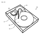
- FIG. 10 is a perspective view showing an outer appearance of a hard disk recording and reproducing device including the light guide according to the present embodiment.
- the light transmission processing unit 2 has a configuration including a light emitting drive portion 5 and a light emitting portion (optical element) 6 .
- the light emitting drive portion 5 drives the light emission of the light emitting portion 6 based on an electrical signal inputted from the outside.
- the light emitting drive portion 5 is configured by a light emission drive IC (Integrated Circuit).
- the light emitting drive portion 5 includes an electrical connecting part with respect to an electrical wiring for transmitting the electrical signal from the outside.
- the light emitting portion 6 emits light based on a drive control by the light emitting drive portion 5 .
- the light emitting portion 6 is configured by a light emitting element such as VCSEL (Vertical Cavity-Surface Emitting Laser).
- a light incident side end of the light guide 4 is irradiated with the light emitted from the light emitting portion 6 as a light signal.
- the IC may be configured on the outside.
- the light reception processing unit 3 has a configuration including an amplifier 7 and a light receiving portion (optical element) 8 .
- the light receiving portion 8 receives the light serving as a light signal exit from a light exit side end of the light guide 4 , and outputs an electrical signal through photoelectric conversion.
- the light receiving portion 8 is configured by a light receiving element such as PD (Photo-Diode).
- the amplifier 7 amplifies the electric signal outputted from the light receiving portion 8 and outputs the same to the outside.
- the amplifier 7 is configured by amplification IC, for example.
- the amplifier 7 includes an electrical connecting part with respect to the electrical wiring for transmitting the electrical signal to the outside.
- FIG. 3 schematically shows the state of light transmission in the light guide 4 .
- the light guide 4 is configured by a column-shaped member having flexibility.
- a light incident surface 4 A is arranged at the light incident side end of the light guide 4
- a light exit surface 4 B is arranged at the light exit side end.
- the light exit from the light emitting portion 6 enters from a direction perpendicular to the light transmission direction of the light guide 4 with respect to the light incident side end of the light guide 4 .
- the incident light advances through the light guide 4 by being reflected at the light incident surface 4 A.
- the light that advances through the light guide 4 and reaches the light exit side end is reflected at the light exit surface 4 B and exits in a direction perpendicular to the light transmission direction of the light guide 4 .
- the light receiving portion 8 is irradiated with the exit light, and photoelectric conversion is performed in the light receiving portion 8 .
- the light emitting portion 6 serving as a light source can be arranged in a horizontal direction with respect to the light transmission direction with respect to the light guide 4 .
- the light emitting portion 6 is installed between the light guide 4 and the substrate surface so as to emit light in the normal direction of the substrate surface.
- the mounting becomes easier than the configuration of installing the light emitting portion 6 so as to emit light parallel to the substrate surface.
- application can be made to the configuration of using a plane mounting light emitting element in which the electrode and the light emitting portion are in the same plane.
- the optical module 1 of the present embodiment has a configuration in which the signal light propagated through the light guide 4 is reflected by the light exit surface 4 B and guided to the light receiving portion 8 (i.e., configuration of using the light exit surface 4 B as the reflection surface for changing the optical path), but the configuration of the optical module 1 is not limited to such a configuration, and may be any configuration as long as the signal light exit from the light exit surface 4 B can be received by the light receiving portion 8 .
- the light guide 4 may have a configuration in which the light exit surface 4 B does not function as the reflection surface, and the signal light may exit in the light transmission direction from the light exit surface 4 B.
- the light receiving portion 8 is arranged such that the light receiving surface is in a direction perpendicular to the substrate surface (i.e., direction perpendicular to the light transmission direction) so as to receive the signal light exit in the light transmission direction from the light exit surface 4 B.
- the package of the present embodiment includes a supporting portion for supporting the light exit side end (or light incident side end) of the light guide 4 , and an accommodating portion for accommodating the light emitting portion 6 or the light receiving portion 8 serving as the optical element, where a lead frame connecting to the optical element is interiorly arranged.
- FIGS. 1( a ) to ( c ) show a top view, bottom view, and cross-sectional view of the package of the present embodiment.
- FIGS. 1( b ) and ( c ) are cross-sectional views showing an outline of the manufacturing method of the package of the present embodiment.
- a package 20 of the present embodiment has a lead frame 9 arranged in a resin unit 10 .
- the resin unit 10 is formed with a supporting portion 10 a for supporting the light guide 4 , an accommodating portion 10 b for accommodating an optical element 12 and a signal processing circuit 13 (correspond to light emitting drive portion 5 or amplifier 7 shown in FIG. 2) , and an opening 10 c.
- the supporting portion 10 a is formed adjacent to the accommodating portion 10 b .
- the supporting portion 10 a is formed as part of a side wall forming the accommodating portion 10 b.
- the lead frame 9 is exposed at the accommodating portion 10 b .
- an optical element mounting surface 9 a for mounting the optical element, and a signal processing circuit mounting surface 9 c for mounting the signal processing circuit are arranged.
- the side mounted with the optical element 12 is the upper side (front side), and the opposite side is the lower side (back side) in the lead frame 9 .
- a back surface 9 c opposite to the optical element mounting surface 9 a of the lead frame 9 is exposed.
- the opening 10 c of the resin unit 10 is formed on the back side of the optical element mounting surface 9 a in the lead frame 9 , and the back surface 9 c also serves as a surface on the upper side of the surfaces forming the opening 10 c.
- the package 20 has a characteristic in that the supporting portion 10 a , the accommodating portion 10 b , and the opening 10 c of the resin unit 10 are integrally molded by a die. The manufacturing method of the package 20 will be described below.
- the manufacturing method of the package 20 includes an integral molding step of integrally molding the resin unit 10 using an integral molding die 11 shown in FIG. 1( c ).
- the lead frame 9 is prepared, as shown in FIG. 1( b ).
- the lead frame 9 is set in the die 11 , and resin is injected from a resin injection port 11 d of the die 11 . After filling the resin into the die 11 , the resin is cured and then the die 11 is detached to thereby manufacture the package 20 .
- the die 11 includes a recess 11 a for forming the supporting portion 10 a , a first projection 11 b for forming the accommodating portion 10 b , and a second projection 11 c for forming the opening 10 c .
- the first projection 11 b comes into contact with the optical element mounting surface 9 a of the lead frame 9
- the second projection 11 c comes into contact with the back surface 9 b opposite to the optical element mounting surface 9 a .
- the first projection 11 b and the second projection 11 c form a sandwiching portion for sandwiching and holding both surfaces, the front surface and the back surface, of the optical element mounting portion of the lead frame 9 .
- the die 11 sandwiches the optical element mounting portion when both surfaces, the optical element mounting surface 9 a and the back surface 9 b , come into contact with the first projection 11 b and the second projection 11 c , respectively. Accordingly, when the lead frame 9 is set in the die 11 , the optical element mounting surface 9 a of the lead frame 9 becomes a flat surface without warp etc. Therefore, the package 20 manufactured through integral molding by the die 11 can prevent the warp of the optical element mounting surface 9 a at the lead frame. Therefore, in the package 20 , the optical element mounting surface 9 a and the upper surface of the supporting portion 10 a are formed with satisfactory accuracy by the die, and the positional accuracy required to maintain the positional relationship of the flexible light guide end and the optical element constant can be satisfied. In the package 20 , the positional relationship of the flexible light guide end and the optical element can be maintained at the positional accuracy of 5 ⁇ m, for example.
- a die where both surfaces of the optical element mounting surface 9 a and the back surface 9 b come into contact with the first projection 11 b and the second projection 11 c , respectively, so that the optical element mounting portion is sandwiched is used for the die 11 .
- a die that sandwiches the signal processing circuit mounting surface 9 c and the back surface opposite thereto in addition to the optical element mounting portion may be used. Therefore, the positional accuracy required to maintain the positional relationship of the flexible light guide end and the optical element constant is satisfied, and the signal processing circuit can be stably mounted on the accommodating portion 10 b.
- FIG. 4 shows a cross-sectional view of the light guide 4 that can be mounted in the package 20 .
- the light guide 4 has a configuration including a column-shaped core 4 a having the light transmission direction as the axis, and a clad 4 b arranged to surround the periphery of the core 4 a .
- the core 4 a and the clad 4 b are made of material having translucency, and the index of refraction of the core 4 a is higher than the index of refraction of the clad 4 b .
- the light signal that entered the core 4 a is transmitted in the light transmission direction by repeating total reflection inside the core 4 a .
- the end face at the light guide 4 is not perpendicular to the optical axis (X-axis), and is cut diagonally to thereby form the optical path changing mirror surface 4 d .
- the end face of the light guide 4 is perpendicular to the XY plane and is inclined so as to form an angle ⁇ ( ⁇ 90° with respect to the X-axis.
- the signal light transmitting through the core 4 a is reflected by the optical path changing mirror surface 10 D so that the advancing direction is changed, and exit from the optical path changing mirror surface 4 d towards the optical element 12 .
- the light receiving surface (or light emitting surface) of the optical element 12 is arranged facing the light exit surface (or incident surface) of the light guide 4 .
- FIG. 5 shows a cross-sectional view taken along a plane perpendicular to the light transmission direction of the package 20 serving as a second variant.
- the areas of the optical element mounting surface 9 a and the back surface 9 b thereof of the lead frame 9 are substantially the same, but the area of the back surface 9 b may be smaller than the area of the optical element mounting surface 9 a , as shown in FIG. 5 .
- the back surface 9 b corresponding to the surface on the upper side of the surfaces forming the opening 10 c has a smaller area than the optical element mounting surface 9 a .
- the opening 10 c has a configuration in which the interval between the side walls forming the opening 10 c becomes greater towards the lower side from the back surface 9 c.
- the package 20 of the second variant can be manufactured using the die 11 in which the contacting area with the back surface 9 b of the second projection 11 c is smaller than the contacting area with the optical element mounting surface 9 a of the first projection 11 b in the integral molding step shown in FIG. 1( c ).
- the opening 10 c shown in FIG. 5 is manufactured through integral molding by using the die 11 in which the second projection 11 c has a tapered shape which outer periphery becomes larger towards the lower side.
- FIG. 6 shows a cross-sectional view taken along a plane perpendicular to the light transmission direction of the package 20 serving as the third variant.
- the back surface of the lead frame 9 is exposed at the opening 10 c , but resin (resin filled portion 14 ) may be filled in the opening 10 c , as shown in FIG. 6 .
- the back surface 9 b of the lead frame 9 thus is not exposed to the outside and can be protected from static electricity at outside the optical module by filling resin in the opening 10 c . Furthermore, corrosion of the back surface 9 b of the lead frame 9 can be prevented.
- the package 20 shown in FIG. 6 can be manufactured by performing a resin filling step of filling resin in the opening 10 c on the back side of the optical element mounting surface 9 a formed by the second projection 11 c after the integral molding step.
- the resin used in the resin filling step is not particularly limited as long as it is resin that can prevent the exposure of the back surface 9 b of the lead frame 9 .
- the resin used in the resin filling step may be the same resin as the resin used in the integral molding step (resin forming resin unit 10 ), or may be a different resin.
- FIG. 7 shows a cross-sectional view taken along a plane perpendicular to the light transmission direction of the package 20 serving as a fourth variant.
- the back surface of the lead frame 9 is exposed at the opening 10 c , but the surface (back surface 9 b ) on the upper side of the opening 10 c may be subjected to plating process (plating portion 15 ), as shown in FIG. 7 .
- the back surface 9 b of the lead frame 9 is not exposed to the outside and the corrosion of the back surface 9 b of the lead frame 9 can be prevented by adopting the configuration in which the plating process is performed on the surface (back surface 9 b ) on the upper side of the opening 10 c.
- the opening 10 c formed with the plating portion 15 may be used as a test terminal for testing an operation check etc. of the optical element such as VCSEL and PD.
- an extra terminal does not need to be set as the test terminal at the exterior of the package 20 , and the step can be simplified.
- the back surface 9 b of the lead frame 9 can be easily protected by filing the opening 10 c with resin and the like after the test by the test terminal.
- optical module 1 of the present embodiment can be applied to the following application examples.
- a foldable electronic device such as a foldable portable telephone, a foldable PHS (Personal Handyphone System), a foldable PDA (Personal Digital Assistant), and a foldable notebook computer.
- a foldable electronic device such as a foldable portable telephone, a foldable PHS (Personal Handyphone System), a foldable PDA (Personal Digital Assistant), and a foldable notebook computer.
- FIGS. 8 ( a ) to ( c ) show an example in which the light guide 4 is applied to a foldable portable telephone 40 .
- FIG. 8( a ) is a perspective view showing an outer appearance of the foldable portable telephone 40 incorporating the light guide 4 .
- FIG. 8( b ) is a block diagram of a portion where the light guide 4 is applied in the foldable portable telephone 40 shown in FIG. 8( a ).
- a control unit 41 arranged on a body 40 a side in the foldable portable telephone 40 an external memory 42 , a camera (digital camera) 43 , and a display unit (liquid crystal display) 44 arranged on a lid (drive portion) 40 b side rotatably arranged at one end of the body with the hinge portion as a shaft are connected by the light guide 4 .
- FIG. 8( c ) is a perspective plan view of the hinge portion (portion surrounded with a broken line) in FIG. 8( a ).
- the light guide 4 is wrapped around a supporting rod at the hinge portion and bent to thereby connect the control unit arranged on the body side, and the external memory 42 , the camera 43 , and the display unit 44 arranged on the lid side.
- High speed and large capacity communication can be realized in a limited space by applying the light guide 4 to the foldable electronic device. Therefore, it is particularly suitable in devices where high speed and large capacity data communication is necessary and miniaturization is demanded such as the foldable liquid crystal display.
- the light guide 4 is applied to a device having a drive portion such as a printer head in a printing device (electronic device) and a reading unit in a hard disk recording and reproducing device.
- FIGS. 9( a ) to ( c ) show an example in which the light guide 4 is applied to a printing device 50 .
- FIG. 9( a ) is a perspective view showing an outer appearance of the printing device 50 .
- the printing device 50 includes a printer head 51 for performing printing on a paper 52 while moving in a width direction of a paper 52 , where one end of the light guide 4 is connected to the printer head 51 .
- FIG. 9( b ) is a block diagram of a portion where the light guide 4 is applied in the printing device 50 . As shown in the figure, one end of the light guide 4 is connected to the printer head 51 , and the other end is connected to a body side substrate in the printing device 50 .
- the body side substrate includes control means etc. for controlling the operation of each unit of the printing device 50 , and the like.
- FIG. 9( c ) and FIG. 9( d ) are perspective views showing a curved state of the light guide 4 when the printer head 51 is moved (driven) in the printing device 50 .
- the curved state of the light guide 4 changes by the drive of the printer head 51 and each position of the light guide 4 repeatedly curves.
- the optical module 1 according to the present embodiment is suited for such a drive portion. High speed and large capacity communication using the drive portion can be realized by applying the optical module 1 to such drive portions.
- FIG. 10 shows an example in which the light guide 4 is applied to a hard disk recording and reproducing device 60 .
- the optical module according to the present invention has a configuration in which the optical element and the light transmission path are mounted on the package, as described above.
- the manufacturing method of the package according to the present invention preferably uses a die in which the contacting area with the back surface of the second projection is smaller than the contacting area with the optical element mounting surface of the first projection in the integral molding step.
- the manufacturing method of the package according to the present invention preferably includes a plating step of performing a plating process on the opening on the back side of the optical element mounting surface formed by the second projection after the integral molding step.
- the back surface of the lead frame is not exposed to the outside, and the corrosion of the back surface of the lead frame can be prevented.
Landscapes
- Physics & Mathematics (AREA)
- General Physics & Mathematics (AREA)
- Optics & Photonics (AREA)
- Engineering & Computer Science (AREA)
- Microelectronics & Electronic Packaging (AREA)
- Signal Processing (AREA)
- Condensed Matter Physics & Semiconductors (AREA)
- Electromagnetism (AREA)
- Optical Couplings Of Light Guides (AREA)
- Encapsulation Of And Coatings For Semiconductor Or Solid State Devices (AREA)
Applications Claiming Priority (3)
| Application Number | Priority Date | Filing Date | Title |
|---|---|---|---|
| JP2007-061044 | 2007-03-09 | ||
| JP2007061044 | 2007-03-09 | ||
| PCT/JP2008/054188 WO2008111524A1 (ja) | 2007-03-09 | 2008-03-07 | パッケージの製造方法、パッケージ、光モジュール、及び一体成型用金型 |
Publications (2)
| Publication Number | Publication Date |
|---|---|
| US20100104240A1 US20100104240A1 (en) | 2010-04-29 |
| US8218917B2 true US8218917B2 (en) | 2012-07-10 |
Family
ID=39759462
Family Applications (1)
| Application Number | Title | Priority Date | Filing Date |
|---|---|---|---|
| US12/530,247 Expired - Fee Related US8218917B2 (en) | 2007-03-09 | 2008-03-07 | Package manufacturing method, package, optical module and die for integral molding |
Country Status (6)
| Country | Link |
|---|---|
| US (1) | US8218917B2 (de) |
| EP (1) | EP2124252A4 (de) |
| JP (1) | JP5170080B2 (de) |
| KR (1) | KR101078518B1 (de) |
| CN (1) | CN101627466B (de) |
| WO (1) | WO2008111524A1 (de) |
Cited By (8)
| Publication number | Priority date | Publication date | Assignee | Title |
|---|---|---|---|---|
| US9094135B2 (en) | 2013-06-10 | 2015-07-28 | Freescale Semiconductor, Inc. | Die stack with optical TSVs |
| US9091820B2 (en) | 2013-06-10 | 2015-07-28 | Freescale Semiconductor, Inc. | Communication system die stack |
| US9261556B2 (en) | 2013-06-10 | 2016-02-16 | Freescale Semiconductor, Inc. | Optical wafer and die probe testing |
| US9435952B2 (en) | 2013-06-10 | 2016-09-06 | Freescale Semiconductor, Inc. | Integration of a MEMS beam with optical waveguide and deflection in two dimensions |
| US9442254B2 (en) | 2013-06-10 | 2016-09-13 | Freescale Semiconductor, Inc. | Method and apparatus for beam control with optical MEMS beam waveguide |
| US9766409B2 (en) | 2013-06-10 | 2017-09-19 | Nxp Usa, Inc. | Optical redundancy |
| US9810843B2 (en) | 2013-06-10 | 2017-11-07 | Nxp Usa, Inc. | Optical backplane mirror |
| US10230458B2 (en) | 2013-06-10 | 2019-03-12 | Nxp Usa, Inc. | Optical die test interface with separate voltages for adjacent electrodes |
Families Citing this family (2)
| Publication number | Priority date | Publication date | Assignee | Title |
|---|---|---|---|---|
| EP2124252A4 (de) * | 2007-03-09 | 2012-10-17 | Omron Tateisi Electronics Co | Kapselungsherstellungsverfahren, kapselung, optisches modul und chip für integrale formung |
| CN102057306A (zh) * | 2008-06-10 | 2011-05-11 | 住友电木株式会社 | 电子设备、便携电话机、挠性电缆、光波导形成体的制造方法 |
Citations (8)
| Publication number | Priority date | Publication date | Assignee | Title |
|---|---|---|---|---|
| US4410469A (en) * | 1980-11-28 | 1983-10-18 | Tokyo Shibaura Denki Kabushiki Kaisha | Method for manufacturing a module for a fiber optic link |
| US5099307A (en) * | 1990-03-13 | 1992-03-24 | Sumitomo Electric Industries, Ltd. | Process for producing optical module |
| US5127071A (en) * | 1990-03-13 | 1992-06-30 | Sumitomo Electric Industries, Ltd. | Optical module including receptacle, and method of producing the same |
| JPH06151699A (ja) | 1992-11-06 | 1994-05-31 | Fuji Electric Co Ltd | 半導体装置 |
| US5537737A (en) * | 1992-01-22 | 1996-07-23 | Sumitomo Electric Industries, Ltd. | Method for manufacturing an optical module |
| JPH11111746A (ja) | 1997-10-07 | 1999-04-23 | Miyazaki Oki Electric Co Ltd | 半導体装置の製造方法及びその製造装置 |
| JPH11287926A (ja) | 1997-03-13 | 1999-10-19 | Nippon Telegr & Teleph Corp <Ntt> | 光素子実装基板、該実装基板を用いた光モジュール、およびそれらの製造方法 |
| US20100104240A1 (en) * | 2007-03-09 | 2010-04-29 | Omron Corporation | Package manufacturing method, package, optical module and die for integral molding |
Family Cites Families (13)
| Publication number | Priority date | Publication date | Assignee | Title |
|---|---|---|---|---|
| JPH03228356A (ja) * | 1990-02-02 | 1991-10-09 | Mitsubishi Electric Corp | Icパッケージ |
| JPH0677252U (ja) * | 1993-03-30 | 1994-10-28 | 住友金属工業株式会社 | Icパッケージ |
| JP2785770B2 (ja) * | 1995-10-19 | 1998-08-13 | 日本電気株式会社 | 樹脂封止半導体装置の製造方法およびその製造装置 |
| US5869883A (en) * | 1997-09-26 | 1999-02-09 | Stanley Wang, President Pantronix Corp. | Packaging of semiconductor circuit in pre-molded plastic package |
| JP2001077248A (ja) * | 1999-09-01 | 2001-03-23 | Matsushita Electronics Industry Corp | 半導体装置およびその製造方法 |
| JP2001108870A (ja) * | 1999-10-06 | 2001-04-20 | Mitsubishi Electric Corp | 光デバイス及びその製造方法 |
| US6821027B2 (en) * | 2000-10-16 | 2004-11-23 | Opti Japan Corporation | Miniaturized parallel optical transmitter and receiver module |
| JP2003163303A (ja) * | 2001-11-27 | 2003-06-06 | Alps Electric Co Ltd | Ic実装用基板およびその製造方法 |
| JP2004200331A (ja) * | 2002-12-18 | 2004-07-15 | Renesas Technology Corp | 光通信装置 |
| JP2005197369A (ja) * | 2004-01-05 | 2005-07-21 | Toshiba Corp | 光半導体装置 |
| JP2005294736A (ja) * | 2004-04-05 | 2005-10-20 | Stanley Electric Co Ltd | 半導体発光装置の製造方法 |
| JP4608294B2 (ja) * | 2004-11-30 | 2011-01-12 | 日亜化学工業株式会社 | 樹脂成形体及び表面実装型発光装置並びにそれらの製造方法 |
| JP4478007B2 (ja) * | 2004-12-16 | 2010-06-09 | 日立オートモティブシステムズ株式会社 | 電子回路装置及びその製造方法 |
-
2008
- 2008-03-07 EP EP08721606A patent/EP2124252A4/de not_active Withdrawn
- 2008-03-07 KR KR1020097018484A patent/KR101078518B1/ko not_active Expired - Fee Related
- 2008-03-07 JP JP2009504034A patent/JP5170080B2/ja not_active Expired - Fee Related
- 2008-03-07 US US12/530,247 patent/US8218917B2/en not_active Expired - Fee Related
- 2008-03-07 CN CN2008800074559A patent/CN101627466B/zh not_active Expired - Fee Related
- 2008-03-07 WO PCT/JP2008/054188 patent/WO2008111524A1/ja not_active Ceased
Patent Citations (8)
| Publication number | Priority date | Publication date | Assignee | Title |
|---|---|---|---|---|
| US4410469A (en) * | 1980-11-28 | 1983-10-18 | Tokyo Shibaura Denki Kabushiki Kaisha | Method for manufacturing a module for a fiber optic link |
| US5099307A (en) * | 1990-03-13 | 1992-03-24 | Sumitomo Electric Industries, Ltd. | Process for producing optical module |
| US5127071A (en) * | 1990-03-13 | 1992-06-30 | Sumitomo Electric Industries, Ltd. | Optical module including receptacle, and method of producing the same |
| US5537737A (en) * | 1992-01-22 | 1996-07-23 | Sumitomo Electric Industries, Ltd. | Method for manufacturing an optical module |
| JPH06151699A (ja) | 1992-11-06 | 1994-05-31 | Fuji Electric Co Ltd | 半導体装置 |
| JPH11287926A (ja) | 1997-03-13 | 1999-10-19 | Nippon Telegr & Teleph Corp <Ntt> | 光素子実装基板、該実装基板を用いた光モジュール、およびそれらの製造方法 |
| JPH11111746A (ja) | 1997-10-07 | 1999-04-23 | Miyazaki Oki Electric Co Ltd | 半導体装置の製造方法及びその製造装置 |
| US20100104240A1 (en) * | 2007-03-09 | 2010-04-29 | Omron Corporation | Package manufacturing method, package, optical module and die for integral molding |
Non-Patent Citations (4)
| Title |
|---|
| espacenet.com Abstract; Publication No. JP11111746A dated Apr. 23, 1999; Miyazaki Oki Denki KK; Oki Electric Ind. Co. Ltd. (1 page). |
| espacenet.com Abstract; Publication No. JP11287926A dated Oct. 19, 1999; Nippon Telegraph & Telephone Corp. (1 page). |
| espacenet.com Abstract; Publication No. JP6151699A dated May 31, 1994; Fuji Electric Co. Ltd. (1 page). |
| International Search Report w/translation from PCT/JP2008/054188 dated May 1, 2008 (2 pages). |
Cited By (8)
| Publication number | Priority date | Publication date | Assignee | Title |
|---|---|---|---|---|
| US9094135B2 (en) | 2013-06-10 | 2015-07-28 | Freescale Semiconductor, Inc. | Die stack with optical TSVs |
| US9091820B2 (en) | 2013-06-10 | 2015-07-28 | Freescale Semiconductor, Inc. | Communication system die stack |
| US9261556B2 (en) | 2013-06-10 | 2016-02-16 | Freescale Semiconductor, Inc. | Optical wafer and die probe testing |
| US9435952B2 (en) | 2013-06-10 | 2016-09-06 | Freescale Semiconductor, Inc. | Integration of a MEMS beam with optical waveguide and deflection in two dimensions |
| US9442254B2 (en) | 2013-06-10 | 2016-09-13 | Freescale Semiconductor, Inc. | Method and apparatus for beam control with optical MEMS beam waveguide |
| US9766409B2 (en) | 2013-06-10 | 2017-09-19 | Nxp Usa, Inc. | Optical redundancy |
| US9810843B2 (en) | 2013-06-10 | 2017-11-07 | Nxp Usa, Inc. | Optical backplane mirror |
| US10230458B2 (en) | 2013-06-10 | 2019-03-12 | Nxp Usa, Inc. | Optical die test interface with separate voltages for adjacent electrodes |
Also Published As
| Publication number | Publication date |
|---|---|
| JPWO2008111524A1 (ja) | 2010-06-24 |
| EP2124252A4 (de) | 2012-10-17 |
| KR101078518B1 (ko) | 2011-10-31 |
| JP5170080B2 (ja) | 2013-03-27 |
| EP2124252A1 (de) | 2009-11-25 |
| CN101627466A (zh) | 2010-01-13 |
| CN101627466B (zh) | 2011-08-03 |
| WO2008111524A1 (ja) | 2008-09-18 |
| US20100104240A1 (en) | 2010-04-29 |
| KR20090107564A (ko) | 2009-10-13 |
Similar Documents
| Publication | Publication Date | Title |
|---|---|---|
| US8218917B2 (en) | Package manufacturing method, package, optical module and die for integral molding | |
| CN101765794B (zh) | 薄膜光波导封装、薄膜光波导模块以及电子设备 | |
| JP5309990B2 (ja) | 光伝送モジュール、電子機器 | |
| US8705908B2 (en) | Optical transmission module, method for manufacturing optical transmission module, and electronic device | |
| JP5157964B2 (ja) | 光伝送モジュール、電子機器、及び光伝送モジュールの製造方法 | |
| US8457455B2 (en) | Optical waveguide, optical waveguide module, and electronic apparatus | |
| JP5077342B2 (ja) | 光伝送路パッケージ、光伝送モジュール、電子機器、および、光伝送モジュールの製造方法 | |
| US20100303412A1 (en) | Optical transmission module and electronic device | |
| US8168940B2 (en) | Optical transmission module, electronic device and method for manufacturing optical transmission module | |
| CN101784933B (zh) | 具备增强光传输模块的基板的增强零件的光传输模块及具备该光传输模块的电子设备 | |
| CN101351733B (zh) | 光模块 |
Legal Events
| Date | Code | Title | Description |
|---|---|---|---|
| AS | Assignment |
Owner name: OMRON CORPORATION,JAPAN Free format text: ASSIGNMENT OF ASSIGNORS INTEREST;ASSIGNORS:SANO, AKIHIKO;NOZAWA, HIROTO;YASUDA, NARU;AND OTHERS;SIGNING DATES FROM 20090915 TO 20090928;REEL/FRAME:023437/0225 Owner name: OMRON CORPORATION, JAPAN Free format text: ASSIGNMENT OF ASSIGNORS INTEREST;ASSIGNORS:SANO, AKIHIKO;NOZAWA, HIROTO;YASUDA, NARU;AND OTHERS;SIGNING DATES FROM 20090915 TO 20090928;REEL/FRAME:023437/0225 |
|
| FEPP | Fee payment procedure |
Free format text: PAYOR NUMBER ASSIGNED (ORIGINAL EVENT CODE: ASPN); ENTITY STATUS OF PATENT OWNER: LARGE ENTITY |
|
| REMI | Maintenance fee reminder mailed | ||
| LAPS | Lapse for failure to pay maintenance fees | ||
| STCH | Information on status: patent discontinuation |
Free format text: PATENT EXPIRED DUE TO NONPAYMENT OF MAINTENANCE FEES UNDER 37 CFR 1.362 |
|
| STCH | Information on status: patent discontinuation |
Free format text: PATENT EXPIRED DUE TO NONPAYMENT OF MAINTENANCE FEES UNDER 37 CFR 1.362 |
|
| FP | Lapsed due to failure to pay maintenance fee |
Effective date: 20160710 |