WO2004100367A1 - 圧電振動子ユニット - Google Patents
圧電振動子ユニット Download PDFInfo
- Publication number
- WO2004100367A1 WO2004100367A1 PCT/JP1996/003263 JP9603263W WO2004100367A1 WO 2004100367 A1 WO2004100367 A1 WO 2004100367A1 JP 9603263 W JP9603263 W JP 9603263W WO 2004100367 A1 WO2004100367 A1 WO 2004100367A1
- Authority
- WO
- WIPO (PCT)
- Prior art keywords
- piezoelectric vibrator
- substrate
- electrode
- wiring
- electrodes
- Prior art date
- Legal status (The legal status is an assumption and is not a legal conclusion. Google has not performed a legal analysis and makes no representation as to the accuracy of the status listed.)
- Ceased
Links
Classifications
-
- H—ELECTRICITY
- H03—ELECTRONIC CIRCUITRY
- H03H—IMPEDANCE NETWORKS, e.g. RESONANT CIRCUITS; RESONATORS
- H03H9/00—Networks comprising electromechanical or electro-acoustic elements; Electromechanical resonators
- H03H9/02—Details
- H03H9/05—Holders or supports
- H03H9/10—Mounting in enclosures
- H03H9/1007—Mounting in enclosures for bulk acoustic wave [BAW] devices
- H03H9/1014—Mounting in enclosures for bulk acoustic wave [BAW] devices the enclosure being defined by a frame built on a substrate and a cap, the frame having no mechanical contact with the BAW device
Definitions
- the present invention relates to a surface mount type piezoelectric vibrator cut, and more particularly, to an arrangement of internal wirings thereof.
- FIG. 1 is an exploded perspective view of a conventional piezoelectric vibrator unit.
- the piezoelectric vibrator unit 100 is made up of a ceramic substrate 101, which is an insulating member, a thickness-sliding quartz vibrator 100 (hereinafter referred to as AT quartz vibrator 102), and a ceramic lid 103.
- AT quartz vibrator 102 a thickness-sliding quartz vibrator 100
- ceramic lid 103 On the upper surface of the configured c- substrate 101, there is a rectangular recess 104 for allowing the AT quartz oscillator 102 to escape, and the widthwise direction opposite to the center of the substrate 101 in the longitudinal direction. Separation grooves 105 and 106 are provided at the center and separate the conductive adhesive.
- the AT crystal oscillator 102 is a so-called convex type, in which an excitation electrode 121 and a lead electrode 122 connected thereto are adhered to the upper and lower surfaces by vapor deposition, sputtering or the like.
- the AT crystal unit 102 can be implemented by a so-called rectangular AT plate having a constant thickness.
- the AT crystal oscillator 102 is housed in the concave portion 104 of the substrate 101, and the lead electrodes 122, 123 are fixed to the connection electrodes 107, 110 or 108, 109 with a conductive adhesive. Thereafter, the frequency is appropriately adjusted, and the lid 103 is joined to the substrate 101, whereby the crystal unit 100 is completed.
- FIGS. 2, 3 and 4 show the state of the metal wiring on the substrate 101
- FIG. 2 is a front view
- FIG. 3 is a front view of FIG. 2 viewed from the direction of arrow 130
- the surface of the substrate 101 shown in FIG. 2 is a surface on which the AT crystal unit 102 is mounted (hereinafter, referred to as a mounting surface), and is substantially rectangular.
- the center line in the longitudinal direction of this substantially rectangular shape is defined as the X axis
- the center line in the lateral direction is defined as the Y axis.
- the concave portion 104 is also substantially rectangular, and its center line coincides with the X axis and the Y axis.
- Connection electrodes are provided in portions adjacent to the four corners of the concave portion 104.
- One connection electrode is present in each of the first to fourth quadrants of the XY plane formed by the X axis and the Y axis.
- the first connection electrode 107 and the second connection electrode 108 are sequentially provided from the first quadrant.
- the third connection electrode 109, and the fourth connection electrode 110 are sequentially provided from the first quadrant.
- the separation groove 105 extends between the first and fourth quadrants and is disposed between the first connection electrode 107 and the fourth connection electrode 110 to prevent short-circuiting of these electrodes. .
- the separation groove 106 is disposed between the second connection electrode 108 and the third connection electrode 109 so as to straddle the second and third quadrants, and to prevent a short circuit between these electrodes.
- first external electrodes 1 1 1 1 are provided in regions corresponding to the first, second, third, and fourth quadrants on the upper surface of the substrate 101, respectively.
- a second external electrode 112, a third external electrode 113, and a fourth external electrode 114 are provided.
- the first connection electrode 107 and the second connection electrode 108 are connected by the first metal wiring 1 15, and the first metal wiring 1 15 is further connected by the second metal wiring 1 16 to the second external electrode 1 1 2 It is connected to the.
- the second metal wiring 1 16 extends from the mounting surface of the substrate 101 to the second external electrode 112 on the rear surface via the side surface corresponding to the long side of the mounting surface.
- the second connection electrode 108 is connected to the third external electrode 113 by a third metal wiring 117.
- the third metal wiring 1 17 extends from the second quadrant where the second connection electrode 108 is located to the third quadrant, It bypasses the third connection electrode 109 and reaches the third external electrode 113 via the side surface.
- the first and second connection electrodes 107, 108, the second and third external electrodes 112, 113 are connected to the first, second and third metal wirings 1. They are connected by 15, 11, 16 and 1 17 to form the first group of wiring patterns.
- the third connection electrode 109 and the fourth connection electrode 110 are connected by a fourth metal wiring 118, and the fourth metal wiring 118 is further connected by a fifth metal wiring 119. It is connected to the fourth external electrode 114.
- the fifth metal wiring 119 extends from the mounting surface of the substrate 101 to the fourth external electrode 114 on the rear surface via the side surface corresponding to the long side of the mounting surface.
- the fourth connection electrode 110 is connected to the first external electrode 111 by a sixth metal wiring 120.
- the sixth metal wiring 120 extends from the fourth quadrant where the fourth connection electrode 110 is located to the first quadrant, bypasses the first connection electrode 107, and passes through the side surface to the first external electrode 111. Has reached.
- the third and fourth connection electrodes 109, 110, the fourth and first external electrodes 114, 111 are the fourth, fifth, and sixth metal wirings 111. They are connected by 8, 119, 120 to form a second group of wiring patterns.
- the equivalent parallel capacitance will be described with reference to the equivalent circuit diagrams of the piezoelectric vibrator unit shown in FIGS. 5 and 6.
- the equivalent circuit shown in FIG. 5 is composed of a series circuit of an inductance, a resonance resistance value R, and a capacitance d, and a parallel circuit of a resonator capacitance CoX and the above-described parasitic capacitance Cop between wirings.
- FIG. 6 is an equivalent circuit in which, in the equivalent circuit of FIG. 5, the oscillator capacitance C.sub.X and the parasitic capacitance C.sub.op between the wires are connected as one combined parallel capacitance C.sub.o.
- the parallel capacity Co is represented by the following equation.
- An object of the present invention is to provide a piezoelectric vibrator cut with reduced parasitic capacitance and improved characteristics.
- a piezoelectric vibrator unit is configured such that external electrodes and wirings having different polarities are not arranged on the front and back of a substrate.
- the piezoelectric vibrator has a first excitation electrode provided on a first surface, and a second excitation electrode provided on a second surface, which is a surface on the back side of the first surface.
- at least one first connection electrode connected to the first excitation electrode when the piezoelectric vibrator is mounted, and similarly connected to the second excitation electrode when the piezoelectric vibrator is mounted.
- external electrodes and wirings having different polarities are not located on the front and back with the substrate interposed therebetween, so that the parasitic capacitance can be reduced.
- the substrate may have a concave portion in which at least a part of the piezoelectric vibrator is accommodated in a substantially central portion of a mounting surface on which the piezoelectric vibrator is mounted.
- the board is divided into two parts, each of which is separately wired and It is preferable to form an electrode.
- the substrate is divided into a first substrate and a second substrate by a plane parallel to the mounting surface of the piezoelectric vibrator.
- the first substrate has a through opening corresponding to the concave portion, and the first and second connection electrodes, and further includes a portion provided with the first and second connection electrodes. It has a through hole penetrating the first substrate.
- the second substrate includes the first and second external electrodes, the first and second wirings, and a through-hole receiving portion provided at a position corresponding to the through-hole of the first substrate. have. And a part of the first and second wirings, on a portion corresponding to a bottom surface of the concave portion, on a plane parallel to the mounting surface of the plate on which the piezoelectric vibrator is mounted, the first and second external electrodes, When the first and second wirings are projected, the shadow of the first external electrode and the shadow of the second wiring, and the shadow of the second external electrode and the shadow of the first wiring are arranged so as not to overlap with each other, The external electrodes are avoided.
- the outer shape of the substrate is substantially rectangular
- the concave portion is also substantially rectangular
- the first and second connection electrodes are each two
- four corners of the substantially rectangular concave portion are provided.
- the first and second external electrodes are arranged symmetrically with respect to the center line of the substantially rectangular short direction, and each of the first and second external electrodes is two. Each is arranged symmetrically with respect to the longitudinal center line.
- the total area of the first wiring, the first external electrode, and the first connection electrode; and the total area of the second wiring, the second external electrode, and the second connection electrode are equal.
- the area of the first wiring is equal to the area of the second wiring.
- the distance between wires having different polarities is widened, and the section where the distance is relatively small is reduced.
- wiring is also arranged on the bottom surface of the concave portion of the substrate.
- a first excitation electrode is provided on a first surface
- a second excitation electrode is provided on a second surface, which is a surface on the back side of the first surface.
- the substrate on which the piezoelectric vibrator is mounted has a ⁇ portion in which at least a part of the piezoelectric vibrator is accommodated in a substantially central portion of a mounting surface on which the piezoelectric vibrator is mounted, and Similarly, at least one first connection electrode connected to the first excitation electrode when the vibrator is mounted, At least one second connection electrode connected to the second excitation electrode when mounted, and at least one first external electrode on the back surface side with respect to the mounting surface of the piezoelectric vibrator; A second wiring that has one second external electrode and further connects the first connection electrode and the first external electrode; and a second wiring that connects the second connection electrode and the second external electrode.
- the lid covers a surface of the substrate on which the piezoelectric vibrator is mounted in a state where the piezoelectric vibrator is mounted on the substrate, and hermetically accommodates the piezoelectric vibrator together with the substrate.
- the substrate is divided into a first substrate and a second substrate by a plane parallel to the mounting surface of the piezoelectric vibrator.
- the first substrate has a through opening corresponding to the recess, and the first and second connection electrodes, and further includes a portion provided with the first and second connection electrodes. It has a through hole penetrating the first substrate.
- the second substrate has the first and second external electrodes, the first and second wirings, and a through-hole receiver provided at a position corresponding to the through-hole of the first substrate. ing. At least a part of the first and second wirings is arranged on a surface on the second substrate corresponding to a bottom surface of the concave portion.
- the wiring pattern since the wiring is also arranged on the bottom surface of the concave portion of the substrate, the wiring pattern has a margin, and the interval between the wirings having different polarities can be widened.
- the outer shape of the substrate is substantially rectangular
- the concave portion is also substantially rectangular
- the first and second connection electrodes are each two
- four corners of the substantially rectangular concave portion are provided.
- the first and second external electrodes are each arranged symmetrically with respect to the center line of the substantially rectangular short direction, and each of the first and second external electrodes is two. Each is arranged symmetrically with respect to the longitudinal center line.
- the first and second wirings do not cross the longitudinal center line of the recess inside the recess.
- FIG. 1 is an exploded perspective view of a conventional piezoelectric vibrator unit.
- FIG. 2 is a diagram showing wiring and electrodes arrangement of a conventional piezoelectric vibrator unit.
- FIG. 3 is a diagram showing the arrangement of wiring and electrodes of a conventional piezoelectric vibrator unit.
- FIG. 4 is a diagram showing an arrangement of electrodes of a conventional piezoelectric vibrator unit.
- Fig. 5 This is an equivalent circuit of the piezoelectric vibrator unit.
- Fig. 6 This is the equivalent circuit of the piezoelectric vibrator unit.
- FIG. 7 is an exploded perspective view of the piezoelectric vibrator unit of the embodiment according to the present invention.
- FIG. 8 is a diagram showing the arrangement of wiring and electrodes on a second insulating substrate of the piezoelectric vibrator unit of the present embodiment.
- FIG. 7 is an exploded perspective view of a piezoelectric vibrator tut of the present embodiment.
- the piezoelectric vibrator cut is composed of a ceramic insulating substrate 1 as an insulating member, a thickness-sliding quartz vibrator 2 (hereinafter referred to as an AT quartz vibrator 2), and a ceramic lid 3.
- the insulating substrate 1 is configured by laminating a first insulating substrate 1a and a second insulating substrate 1b.
- the joint surface between the first insulating substrate 1a and the second insulating substrate 1b, the upper surface of the first insulating substrate 1a, and the lower surface of the second insulating substrate lb are parallel to each other.
- the first insulating substrate 1a is thinner than the second insulating substrate 1b, and has a rectangular hollow 4 at the center thereof.
- the hollow 4 forms a recess together with the upper surface of the second insulating substrate 1b.
- the first insulating substrate 1a is provided with separation grooves 5 and 6 which are provided at the center in the short direction on the opposite sides in the longitudinal direction with respect to the center of the insulating substrate 1 and separate the conductive adhesive. ing.
- the AT crystal resonator 2 is a so-called convex type, and an excitation electrode 21 and lead electrodes 22 and 23 connected to the excitation electrode 21 are adhered to the upper and lower surfaces by vapor deposition, sputtering or the like.
- the AT crystal resonator 2 can be implemented with a so-called rectangular AT plate having a constant thickness. After bonding the first insulating substrate 1a and the second insulating substrate 1b, a part of the AT crystal unit 2 is housed in a concave portion of the insulating substrate 1 formed by the hollow 4, and the connection electrodes 7, 1 Leader electrodes 22 and 23 are fixed to 0 or connection electrodes 8 and 9 with a conductive adhesive.
- the AT crystal resonator 2 is placed and fixed on the insulating substrate 1.
- the lid 3 is placed on the insulating substrate 1 so as to cover it from above, and the AT crystal unit 2 is hermetically accommodated together with the insulating substrate 1.
- the upper surface of the first insulating substrate 1a is a surface on which the AT crystal unit 2 is to be mounted.
- the mounting surface which is substantially rectangular.
- the center line in the longitudinal direction of this substantially rectangular shape is set as the X axis
- the center line in the short direction is set as the Y axis.
- the hollow 4 is also substantially rectangular, and its center line coincides with the X axis and the Y axis.
- Connection electrodes are provided in the portions adjacent to the four corners of the hollow 4.
- One connecting electrode is present in each of the first to fourth quadrants of the XY plane formed by the X axis and the Y axis.
- the connection electrode 9 and the fourth connection electrode 10 are described.
- Each of these four connection electrodes 7, 8, 9, 10 has through-holes 7a, 8a, 9a, 10a passing through the back surface of the first insulating substrate 1a, respectively.
- the separation groove 5 is disposed across the first and fourth quadrants and between the first connection electrode 7 and the fourth connection electrode 10 to prevent short-circuiting of these electrodes.
- the separation groove 6 is arranged across the second and third quadrants and between the second connection electrode 8 and the third connection electrode 9 to prevent short-circuiting of these electrodes.
- first external regions are respectively provided in regions corresponding to the first, second, third, and fourth quadrants of the XY plane.
- An electrode 11, a second external electrode 12, a third external electrode 13, and a fourth external electrode 14 are provided.
- FIG. 8 shows details of the pattern of the metal wiring on the upper surface in FIG. 7 of the second insulating substrate 1b. According to this, when the second insulating substrate lb overlaps with the first insulating substrate la, the through holes 7a, 8a, 9a, and 10a are respectively connected to the through holes 7a, 8a, 9a, and 10a. Hole receivers 7b, 8b, 9b, 10b are provided.
- the first through-hole receiver 7b and the second through-hole receiver 8b are connected by a first metal wiring 15.
- the first metal wiring 15 is arranged so as not to cross the X axis so as to bypass the first external electrode 11 existing on the lower surface of the second insulating substrate lb. Thus, when the first metal wiring 15 and the first external electrode 11 are projected on the plane parallel to the mounting surface, the shadows of the first metal wiring 15 and the first external electrode 11 are prevented from overlapping. Further, the first metal wiring 15 is connected to the second external electrode 12 by the second metal wiring 16. 2nd metal wiring
- Numeral 16 extends from the upper surface of the second insulating substrate 1b in FIG. 7 to the second outer electrode 12 on the lower surface via the side surface corresponding to the long side of this surface.
- the second connection electrode 8 is connected to the third external electrode 13 via the through-hole 8 a and the through-hole receiver 8 b via the third metal wiring 17.
- the third metal wiring 17 extends from the second quadrant where the second connection electrode 8 is located to the third quadrant, bypasses the third through-hole receiver 9b, and reaches the third external electrode 13 via the side surface.
- the first and second through-hole receivers 7b, 8b are respectively formed by the first and second through-holes 7a, 8a after the first and second insulating substrates 1a, lb are stacked.
- first and second through-hole receivers 7b and 8b and the second and third external electrodes 12 and 13 are connected to the first, second and third metal wirings 15 and 15, respectively. They are connected by 16 and 17. These connection electrodes, external electrodes, metal wiring, through-holes, and through-hole receivers form a first group of wiring patterns.
- the third through-hole receiver 9b and the fourth through-hole receiver 10b are connected by a fourth metal wiring 18.
- the fourth metal wiring 1 so as not to cross the X-axis, a third outer electrode 1 3 c Yotsute thereto which are arranged so as to bypass the existing on the lower surface of the second insulated substrate 1 b, When the fourth metal wiring 18 and the third external electrode 13 are projected on a plane parallel to the mounting surface, their shadows do not overlap.
- the fourth metal wiring 18 is connected to the fourth external electrode 14 by a fifth metal wiring 19.
- the fifth metal wiring 19 extends from the upper surface of the second insulating substrate 1b shown in FIG. 7 to the fourth external electrode 14 on the rear surface via the side surface corresponding to the long side of this surface.
- the fourth connection electrode 10 is connected to the first external electrode 11 via the through hole 10a and the through hole receiver 10b by the sixth metal wiring 20.
- the sixth metal wiring 20 extends from the fourth quadrant where the fourth connection electrode 10 is located to the first quadrant, bypasses the first connection electrode 7, and reaches the first external electrode 11 via the side surface.
- the third and fourth through-hole receivers 9b and 10b, the fourth and first external electrodes 14 and 11 are connected to the fourth, fifth and sixth metal wirings 18 and Connected by 19, 20.
- the third and fourth through-hole receivers 9 b and 10 b are formed by stacking the first and second insulating substrates 1 a and 1 b and then forming the third and fourth through-holes 9 a and 10 a respectively. It is connected by brazing or adhesive. These connection electrodes, external electrodes, metal wiring, through-holes, and through-hole receivers form a second group of wiring patterns.
- the first and second groups of the above-described wiring patterns are groups having different polarities when a voltage is applied to the AT crystal resonator 2.
- the two wiring pattern groups are point-symmetric with respect to the intersection of the X-axis and Y-axis, that is, the origin of the XY plane. Shape. Therefore, the same characteristics can be obtained regardless of whether the AT crystal resonator 2 is connected to the first connection electrode 7 and the fourth connection electrode 10 or to the second connection electrode 8 and the third connection electrode 9. Can be.
- the metal wiring is arranged on the bottom surface of the recess formed in the insulating substrate 1 by the hollow 4, a space is allowed, and the distance between the metal wirings belonging to different groups is increased.
- the length irn of the section in which these metal wirings are at the distance d 1 can be reduced. Therefore, the parasitic capacitance between metal wires belonging to different groups is reduced.
- the first metal wiring 15 and the third metal wiring 18 are arranged in parallel at substantially the center of the substrate 1, where the section length irn is the distance.
- the reason why the metal wiring is provided on the bottom surface of the concave portion of the insulating substrate 1 is that the insulating substrate 1 is formed by laminating the first insulating substrate 1 a and the second insulating substrate 1 b separately provided with metal wiring and the like. That's because.
- the metal wiring and the external electrode are arranged such that their shadows do not overlap when they are projected on a plane parallel to the mounting surface. Therefore, the parasitic capacitance generated between the metal wiring and the external electrode is reduced.
- first metal wiring 15 and the fourth metal wiring 18 are arranged so as not to cross the X-axis, a conductive adhesive for fixing the AT crystal resonator 2 is spilled and the base metal is spilled. Even if it flows to the bottom of the recess, insulation failure is prevented.
- the prototype experiment was performed on a sample in which the thickness of the second insulating substrate 1b, which is considered to be practical, was 0.5 to 1 mm and the width 23 was 4 to 6 mm.
- the distance between metal wires where the wire-to-wire capacitance C op is 1/3 of the conventional example was 13 to 11 with respect to the width w of the second insulating substrate 1b. This is because if the distance between the metal wires becomes smaller than 1/10 of the width of the second insulating substrate 1b, the capacitance between the wires increases, and the distance di between the metal wires becomes the second insulating substrate.
- the concave portion for accommodating the AT crystal resonator is formed in the insulating substrate.
- the insulating substrate is formed in a substantially planar shape, and the AT crystal resonator on the insulating substrate is mounted. Wiring can also be applied to the portion where it is placed. Thereby, the same effect as in the above-described embodiment can be obtained.
- the AT crystal unit is not a convex type, but a rectangular AT plate having a constant thickness.
Landscapes
- Physics & Mathematics (AREA)
- Acoustics & Sound (AREA)
- Piezo-Electric Or Mechanical Vibrators, Or Delay Or Filter Circuits (AREA)
Description
明細書
発明の名称
圧電振動子ュニット
技術分野
本発明は表面実装型の圧電振動子ュ-ットに関し、 特にその内部配線の配置に 関する。 背景技術
近年パーソナルコンピュータ、 通信機器等のクロック源として用いられる水晶 振動子等の圧電振動子として、 プリント配線基板への表面実装を容易に行えるよ うにした表面実装型の圧電振動子ュニットが用いられている。 このような表面実 装型圧電振動子においては以下のことが公知または試みられている。
( 1 ) 圧電振動子を片持ち支持で搭載し、 両持ち支持した場合に、 容器と振動子 との熱膨脹の差により発生する応力を低減して、 振動子の温度変化に対する振動 特性を改善すること。
( 2 ) 容器への振動子の自動装填を前提として、 容器の接続電極をその長手方向 に 2対設け、 容器及び振動子の長手方向の向きに関係なくセットできるようにし て生産効率を向上させること。
以下、 従来圧電振動子ユニットを図面に従って説明する。
図 1は従来の圧電振動子ュニットの展開斜視図である。 圧電振動子ュニット 1 0 0は絶縁部材であるセラミックの基板 1 0 1、 厚み滑り水晶振動子 1 0 2 (以 下、 A T水晶振動子 1 0 2と記す) 及ぴセラミックの蓋 1 0 3により構成される c 基板 1 0 1の上面には A T水晶振動子 1 0 2を逃げるための矩形の凹部 1 0 4及 ぴこれに基板 1 0 1の中心に関し長手方向に互いに反対側で幅方向の中心部に設 けられ、 導電接着剤を分離する分離溝 1 0 5及び 1 0 6が設けられている。 A T 水晶振動子 1 0 2はいわゆるコンベックス型で励振電極 1 2 1とそれに接続する 引き出し電極 1 2 2が上下面に蒸着、 スパッタリング等で密着されている。 なお、
AT水晶振動子 102は厚み一定のいわゆる矩形 AT板でも実施することができ る。 AT水晶振動子 1 02は基板 10 1の凹部 1 04に収納され、 接続電極 1 0 7、 1 1 0または 1 08、 1 09に引き出し電極 1 22、 1 23が導電接着剤で 固定される。 この後で、 適宜周波数調整が行われて、 基板 10 1に蓋 1 03が接 合されて水晶振動子ュニット 100が完成する。
図 2、 図 3およぴ図 4は基板 1 01の金属配線の状態を示す図で、 図 2は正面 図、 図 3は図 2を矢印 1 30方向から見た矢視正面図、 図 4は図 2の背面図であ る。
図 2に現れる、 基板 1 0 1の面は、 AT水晶振動子 1 0 2を載置する面 (以下、 載置面と記す) であり、 これは略方形である。 以下の説明のために、 この略方形 の長手方向の中心線を X軸、 短手方向の中心線を Y軸とする。 凹部 1 04も略方 形であり、 その中心線は、 前記 X軸、 Y軸に一致している。 凹部 104の四隅に 隣接する部分には接続電極が設けられている。 前記 X軸 Y軸で形成される X Y平 面の第 1象限から第 4象限に各々一つの接続電極が存在し、 以下、 第 1象限から 順に第 1接続電極 1 07、 第 2接続電極 1 08、 第 3接続電極 1 09、 第 4接続 電極 1 10と記す。
分離溝 1 05は第 1象限と第 4象限とに跨がって、 かつ第 1接続電極 107及 び第 4接続電極 1 1 0の間に配置され、 これらの電極のショートを防止している。 分離溝 106は第 2象限と第 3象限に跨がって、 かつ第 2接続電極 1 08及ぴ第 3接続電極 1 09の間に配置され、 これらの電極のショートを防止している。 図 4に示すように、 基板 1 01の背面には、 前記基板 1 01の上面の第 1象限、 第 2象限、 第 3象限及び第 4象限に対応する領域に各々第 1外部電極 1 1 1、 第 2外部電極 1 1 2、 第 3外部電極 1 1 3、 第 4外部電極 1 14が設けられている。 第 1接続電極 107と第 2接続電極 1 08は、 第 1金属配線 1 1 5により接続 され、 さらに第 1金属配線 1 1 5は、 第 2金属配線 1 1 6により第 2外部電極 1 1 2に接続されている。 第 2金属配線 1 1 6は基板 10 1の載置面から載置面の 長辺にあたる側面を経て背面の第 2外部電極 1 1 2に達している。 第 2接続電極 1 08は、 第 3金属配線 1 1 7により第 3外部電極 1 1 3に接続されている。 第 3金属配線 1 1 7は、 第 2接続電極 108のある第 2象限から第 3象限に延び、
第 3接続電極 1 0 9を迂回し、 側面を経て第 3外部電極 1 1 3に達している。 以 上のように、 第 1および第 2接続電極 1 0 7, 1 0 8、 第 2および第 3外部電極 1 1 2, 1 1 3が、 第 1、 第 2およぴ第 3金属配線 1 1 5, 1 1 6, 1 1 7によ り接続され、 配線パターンの第 1グループを形成している。
一方、 第 3接続電極 1 0 9と第 4接続電極 1 1 0は、 第 4金属配線 1 1 8によ り接続され、 さらに第 4金属配線 1 1 8は、 第 5金属配線 1 1 9により第 4外部 電極 1 1 4に接続されている。 第 5金属配線 1 1 9は基板 1 0 1の載置面から載 置面の長辺にあたる側面を経て背面の第 4外部電極 1 1 4に達している。 第 4接 続電極 1 1 0は、 第 6金属配線 1 2 0により第 1外部電極 1 1 1に接続されてい る。 第 6金属配線 1 2 0は、 第 4接続電極 1 1 0のある第 4象限から第 1象限に 延び、 第 1接続電極 1 0 7を迂回し、 側面を経て第 1外部電極 1 1 1に達してい る。 以上のように、 第 3および第 4接続電極 1 0 9, 1 1 0、 第 4およぴ第 1外 部電極 1 1 4, 1 1 1力 第 4、 第 5および第 6金属配線 1 1 8, 1 1 9, 1 2 0により接続され、 配線パターンの第 2グループを形成している。
この従来の圧電振動子ュニットでは、 基板 1 0 1の上面に金属配線が密に配設 されるために、 図 2に示すように異なるグループに属する金属配線間の距離 d。 が短かい区間 m。 が長くなる。 異なるグループの金属配線間では電気的極性が異 なるので、 金属配線間の距離 d。 が短かい区間 m。 が長いと、 この区間に寄生容 量が発生する。 さらに、 基板 1 0 1を挟んで表裏に配置される外部電極と金属配 線のうち、 異なるグループに属するものの間にも寄生容量が発生する。 これらの 寄生容量は、 前記圧電振動子ュニットの等価並列容量を増加させる。
この等価並列容量について図 5およぴ図 6の圧電振動子ュニットの等価回路図 に従って説明する。 図 5に示す等価回路は、 インダクタンスし、 共振抵抗値 R、 及び容量 d の直列回路と、 振動子の容量 C o X及び前述の配線間の寄生容量 C o pとの並列回路で構成される。 図 6は、 図 5の等価回路において、 並列に接続 される振動子容量 C o Xと配線間寄生容量 C o pを、 一つの合成された並列容量 C oとして示した等価回路である。 並列容量 C oは以下の式で表される。
C o = C o + C o ρ … (1 )
前述のように、 従来の圧電振動子ユニットでは、 寄生容量 C o pが大きくなり、
よって並列容量 C oが大きくなるという問題があった。 並列容量が大きくなると、 この圧電振動子ュニットを発振回路に組み込んだ場合に、 発振開始が遅れたり、 発振が不安定になる場合があるいう問題がある。 発明の開示
本発明の目的は、 寄生容量を小さくし、 特性の改善された圧電振動子ュ-ット を提供することにある。
上記目的を達成するために本発明にかかる圧電振動子ュニットは、 異なる極性 となる外部電極と配線が基板を挟んで表裏に配置されないようにしている。 具体 的には、 圧電振動子は、 第 1面に第 1励振電極が設けられ、 前記第 1面の裏側の 面である第 2面に第 2励振電極が設けられている。 また、 前記圧電振動子が載置 された時に前記第 1励振電極に接続される少なくとも一つの第 1接続電極と、 同 様に前記圧電振動子が載置された時に前記第 2励振電極に接続される少なくとも 一つの第 2接続電極とを有し、 前記圧電振動子の载置面に対して裏面側には少な くとも一つの第 1外部電極と少なくとも一つの第 2外部電極を有し、 さらに、 前 記第 1接続電極と前記第 1外部電極を接続する第 1配線と、 前記第 2接続電極と 前記第 2外部電極を接続する第 2配線とを有している。 さらに、 蓋は、 前記圧電 振動子が前記基板に載置された状態で、 前記基板の圧電振動子を載置する面を覆 い、 前記基板とともに前記圧電振動子を密封収容するものである。 そして、 前記 基板の、 圧電振動子の載置面と平行な平面に、 前記第 1および第 2外部電極と、 前記第 1および第 2配線を投影した場合に、 第 1外部電極の影と第 2配線の影、 第 2外部電極の影と第 1配線の影が重ならないように、 これらの外部電極と配線 が配置されている。
このような配置によれば、 異なる極性となる外部電極と配線が基板を挟んで表 裏には位置されることがなく、 寄生容量を減少させることができる。
また、 前記基板は、 前記圧電振動子が載置される載置面のほぼ中央部に前記圧 電振動子の少なくとも一部が納まる凹部を有するようにすることもできる。
さらに、 上記の構成を達成するために、 基板の凹部の底面にも配線を配置する ことが好適である。 このためには、 前記基板を二つに分割し、 各々別個に配線お
ょぴ電極を形成することが好ましい。 好ましい形態においては、 前記基板を、 前 記圧電振動子の載置面に平行な平面により第 1基板と第 2基板に分割する。 前記 第 1基板は、 前記凹部に相当する貫通開口部と、 前記第 1およぴ第 2接続電極と を有し、 さらに、 前記第 1および第 2接続電極の設けられた部分には、 当該第 1 基板を貫通する貫通孔を有している。 一方、 前記第 2基板は、 前記第 1およぴ第 2外部電極と、 前記第 1およぴ第 2配線と、 前記第 1基板の貫通孔に対応する位 置に設けられた貫通孔受けを有している。 そして、 前記第 1および第 2配線の一 部は、 前記凹部の底面に相当する部分に、 前記板の圧電振動子の載置面と平行な 平面に、 前記第 1および第 2外部電極と、 前記第 1および第 2配線を投影した場 合に、 前記第 1外部電極の影と第 2配線の影、 第 2外部電極の影と第 1配線の影 が重ならないよう配置されることによって、 前記外部電極を回避している。
さらに、 本発明の好ましい態様においては、 前記基板の外形は略方形とし、 前 記凹部も略方形とし、 前記第 1および第 2の接続電極は各々 2個であり、 前記略 方形の凹部の四隅に、 略方形の短手方向の中心線に対し対称に配置され、 前記第 1およぴ第 2の外部電極は各々 2個であり、 前記略方形の基板の二つの長辺にそ れぞれ一つずつ長手方向の中心線に対し対称に配置する。
さらに、 本発明の他の好ましい態様においては、 前記第 1配線と第 1外部電極 と第 1接続電極の総面積と、 前記第 2配線と第 2外部電極と第 2接続電極の総面 積とを等しくする。
さらに、 本発明のさらに他の好ましい態様においては、 前記第 1配線の面積と、 前記第 2配線の面積とを等しくする。
さらに、 本発明にかかる他の圧電振動子ユニットは、 異なる極性となる配線間 の距離を広くし、 また前記の距離が比較的小さくなる区間を少なくするようにし ている。 このために、 基板の凹部の底面にも配線を配置している。 具体的には、 圧電振動子は、 第 1面に第 1励振電極が設けられ、 前記第 1面の裏側の面である 第 2面に第 2励振電極が設けられている。 また、 前記圧電振動子を載置する基板 は、 前記圧電振動子が載置される載置面のほぼ中央部に前記圧電振動子の少なく とも一部が納まる囬部を有し、 また前記圧電振動子が載置された時に前記第 1励 振電極に接続される少なくとも一つの第 1接続電極と、 同様に前記圧電振動子が
載置された時に前記第 2励振電極に接続される少なくとも一つの第 2接続電極を 有し、 前記圧電振動子の載置面に対して裏面側には少なくとも一つの第 1外部電 極と少なくとも一つの第 2外部電極を有し、 さらに、 前記第 1接続電極と前記第 1外部電極を接続する第 1配線と、 前記第 2接続電極と前記第 2外部電極を接続 する第 2配線とを有している。 さらに、 蓋は、 前記圧電振動子が前記基板に載置 された状態で、 前記基板の圧電振動子を載置する面を覆い、 前記基板とともに前 記圧電振動子を密封収容する。 そして、 前記基板は、 前記圧電振動子の載置面に 平行な平面により第 1基板と第 2基板に分割されている。 前記第 1基板は、 前記 凹部に相当する貫通開口部と、 前記第 1およぴ第 2接続電極とを有し、 さらに、 前記第 1および第 2接続電極の設けられた部分には、 当該第 1基板を貫通する貫 通孔を有している。 一方、 前記第 2基板は、 前記第 1および第 2外部電極と、 前 記第 1および第 2配線と、 前記第 1基板の貫通孔に対応する位置に設けられた貫 通孔受けを有している。 そして、 前記第 1およぴ第 2配線の少なくとも一部は、 前記凹部の底面に相当する第 2基板上の面に配置されている。
この構成によれば、 基板の凹部の底面にも配線を配置したので配線のパターン に余裕ができ、 異なる極性となる配線の間隔を広くすることが可能となる。 さらに、 本発明の好ましい態様においては、 前記基板の外形を略方形とし、 前 記凹部も略方形とし、 前記第 1および第 2の接続電極は各々 2個であり、 前記略 方形の凹部の四隅に、 略方形の短手方向の中心線に対し対称に配置され、 前記第 1および第 2の外部電極は各々 2個であり、 前記略方形の基板の二つの長辺にそ れぞれ一つずつ長手方向の中心線に対し対称に配置される。
さらに、 本発明の他の好ましい態様においては、 前記第 1および第 2配線は、 前記凹部の内部において、 当該凹部の長手方向の中心線を横切らない。 図面の簡単な説明
図 1 従来の圧電振動子ュニットの分解斜視図である。
図 2 従来の圧電振動子ユニットの配線、 電極の配置を示す図である。
図 3 従来の圧電振動子ユニットの配線、 電極の配置を示す図である。
図 4 従来の圧電振動子ュニットの電極の配置を示す図である。
図 5 圧電振動子ュニットの等価回路である。
図 6 圧電振動子ユエットの等価回路である。
図 7 本発明にかかる実施形態の圧電振動子ュニットの分解斜視図である。
図 8 本実施形態の圧電振動子ユニットの第 2絶縁基板の配線、 電極の配置を示 す図である。 発明を実施するための最良の形態
以下、 本発明の実施の形態 (以下、 実施形態と記す) を図面に従って説明する 図 7は本実施形態の圧電振動子ュュットの展開斜視図である。 圧電振動子ュ-ッ トは絶縁部材であるセラミックの絶縁基板 1、 厚み滑り水晶振動子 2 (以下、 A T水晶振動子 2と記す) 及びセラミックの蓋 3により構成される。 絶縁基板 1は 第 1絶縁基板 1 aと第 2絶縁基板 1 bが積層して構成される。 第 1絶縁基板 1 a と第 2絶縁基板 1 bの接合面と、 第 1絶縁基板 1 aの上面と、 第 2絶緣基板 l b の下面は互いに平行である。 第 1絶縁基板 1 aは第 2絶縁基板 1 bより薄く、 そ の中央部に矩形状の中抜き 4が設けられている。 この中抜き 4は第 1および第 2 の絶縁基板 1 a, l bを積層し絶縁基板 1が形成されたときには、 第 2絶縁基板 1 bの上面と共に凹部を構成する。 さらに第 1絶縁基板 1 aには、 これに絶縁基 板 1の中心に関し長手方向に互いに反対側で短手方向の中心部に設けられ、 導電 接着剤を分離する分離溝 5及び 6が設けられている。
A T水晶振動子 2はいわゆるコンベックス型で励振電極 2 1とそれに接続する 引き出し電極 2 2, 2 3が上下面に蒸着、 スパッタリング等で密着されている。 なお、 A T水晶振動子 2は厚み一定のいわゆる矩形 A T板でも実施することがで きる。 第 1絶縁基板 1 aと第 2絶縁基板 1 bを接着後、 A T水晶振動子 2の一部 は、 中抜き 4により形成された絶縁基板 1の凹部に収納され、 後述する接続電極 7、 1 0または接続電極 8、 9に引き出し電極 2 2、 2 3が導電接着剤で固定さ れる。 この接着によって、 A T水晶振動子 2が絶縁基板 1上に載置、 固定される。 その上から覆い被さるように蓋 3が絶縁基板 1上に載置され、 絶縁基板 1ととも に A T水晶振動子 2を密封収容する。
図 7において、 第 1絶縁基板 1 aの上面は、 A T水晶振動子 2を载置する面
(以下、 載置面と記す) であり、 これは略方形である。 以下の説明のために、 こ の略方形の長手方向の中心線を X軸、 短手方向の中心線を Y軸とする。 中抜き 4 も略方形であり、 その中心線は、 前記 X軸、 Y軸に一致している。 中抜き 4の四 隅に隣接する部分には接続電極が設けられている。 前記 X軸 Y軸で形成される X Y平面の第 1象限から第 4象限に各々一つの接続電極が存在し、 以下、 第 1象限 から順に第 1接続電極 7、 第 2接続電極 8、 第 3接続電極 9、 第 4接続電極 1 0 と記す。 これら 4つの接続電極 7, 8, 9, 1 0の各々は、 第 1絶縁基板 1 aの 裏面に抜ける貫通孔 7 a, 8 a , 9 a , 1 0 aをそれぞれ有している。
分離溝 5は第 1象限と第 4象限とに跨がつて、 かつ第 1接続電極 7及び第 4接 続電極 1 0の間に配置され、 これらの電極のショートを防止している。 分離溝 6 は第 2象限と第 3象限に跨がつて、 かつ第 2接続電極 8及び第 3接続電極 9の間 に配置され、 これらの電極のショートを防止している。
第 2絶縁基板 l bには、 図 7中上面に金属配線が、 下面には、 前述の X Y平面 の第 1象限、 第 2象限、 第 3象限及び第 4象限に対応する領域に各々第 1外部電 極 1 1、 第 2外部電極 1 2、 第 3外部電極 1 3、 第 4外部電極 1 4が設けられて いる。
図 8には、 第 2絶縁基板 1 bの図 7における上面の金属配線のパターンの詳細 が示されている。 これによれば、 第 2絶縁基板 l bには、 第 1絶縁基板 l aと重 なったとき、 前述の貫通孔 7 a, 8 a , 9 a , 1 0 aと接続する位置に、 それぞ れ貫通孔受け 7 b, 8 b, 9 b, 1 0 bが設けられている。
第 1貫通孔受け 7 bと第 2貫通孔受け 8 bは、 第 1金属配線 1 5により接続さ れている。 この第 1金属配線 1 5は X軸を横切らない程度に、 第 2絶縁基板 l b の下面に存在する第 1外部電極 1 1を迂回するように配置されている。 これによ つて、 前述の載置面に平行な平面に第 1金属配線 1 5と第 1外部電極 1 1を投影 した時にこれらの影が重ならないようになつている。 さらに、 第 1金属配線 1 5 は、 第 2金属配線 1 6により第 2外部電極 1 2に接続されている。 第 2金属配線
1 6は第 2絶縁基板 1 bの図 7における上面からこの面の長辺にあたる側面を経 て下面の第 2外部電極 1 2に達している。 第 2接続電極 8は、 貫通孔 8 a、 貫通 孔受け 8 bを経て、 第 3金属配線 1 7により第 3外部電極 1 3に接続されている。
第 3金属配線 1 7は、 第 2接続電極 8のある第 2象限から第 3象限に延び、 第 3 貫通孔受け 9 bを迂回し、 側面を経て第 3外部電極 1 3に達している。 さらに、 第 1およぴ第 2貫通孔受け 7 b, 8 bは、 第 1およぴ第 2絶縁基板 1 a, l bを 重ねた後、 それぞれ第 1および第 2貫通孔 7 a, 8 aとロウづけや接着剤などに より接続される。 以上のように、 第 1およぴ第 2貫通孔受け 7 b, 8 b、 第 2お ょぴ第 3外部電極 1 2, 1 3が、 第 1、 第 2および第 3金属配線 1 5, 1 6, 1 7により接続されている。 これらの接続電極、 外部電極、 金属配線、 貫通孔およ ぴ貫通孔受けが、 配線パターンの第 1グループを形成している。
一方、 第 3貫通孔受け 9 bと第 4貫通孔受け 1 0 bは、 第 4金属配線 1 8によ り接続されている。 この第 4金属配線 1 8は、 X軸を横切らない程度に、 第 2絶 縁基板 1 bの下面に存在する第 3外部電極 1 3を迂回するように配置されている c これによつて、 前述の載置面に平行な平面に第 4金属配線 1 8と第 3外部電極 1 3を投影した時にこれらの影が重ならないようになっている。 さらに第 4金属配 線 1 8は、 第 5金属配線 1 9により第 4外部電極 1 4に接続されている。 第 5金 属配線 1 9は図 7に示す第 2絶縁基板 1 bの上面からこの面の長辺にあたる側面 を経て背面の第 4外部電極 1 4に達している。 第 4接続電極 1 0は、 貫通孔 1 0 a、 貫通孔受け 1 0 bを経て、 第 6金属配線 2 0により第 1外部電極 1 1に接続 されている。 第 6金属配線 2 0は、 第 4接続電極 1 0のある第 4象限から第 1象 限に延び、 第 1接続電極 7を迂回し、 側面を経て第 1外部電極 1 1に達している。 以上のように、 第 3およぴ第 4貫通孔受け 9 b, 1 0 b、 第 4および第 1外部電 極 1 4, 1 1が、 第 4、 第 5および第 6金属配線 1 8, 1 9, 2 0により接続さ れている。
さらに、 第 3および第 4貫通孔受け 9 b , 1 0 bは、 第 1および第 2絶縁基板 1 a , 1 bを重ねた後、 それぞれ第 3および第 4貫通孔 9 a, 1 0 aとロウづけ や接着剤などにより接続される。 これらの接続電極、 外部電極、 金属配線、 貫通 孔および貫通孔受けが、 配線パターンの第 2グループを形成している。
前述の配線パターンの第 1と第 2グループは、 A T水晶振動子 2に電圧を印加 する際に、 互いに異なる極性となるグループである。 また、 この二つの配線パタ ーンのグループは、 X軸, Y軸の交点すなわち X Y平面の原点に対して点対称な
形状である。 したがって、 A T水晶振動子 2が第 1接続電極 7と第 4接続電極 1 0に接続されても、 第 2接続電極 8と第 3接続電極 9に接続されても同一のの特 性を得ることができる。
以上の本実施形態によれば、 中抜き 4によって、 絶縁基板 1に形成される凹き の底面に金属配線を配置したので、 スペースに余裕ができ、 異なるグループに属 する金属配線の距離 を大きくすることができ、 またこれら金属配線が距離 d 1 となっている区間の長さ irn も短くすることができる。 よって、 異なるグルー プに属する金属配線間の寄生容量が小さくなる。 本実施形態においては、 第 1金 属配線 1 5と第 3金属配線 1 8が基板 1のほぼ中央部で平行に配置され、 ここで 区間長さ irn で距離 となっている。
このように、 金属配線を絶縁基板 1の凹部の底面に設けられたのは、 絶縁基板 1を、 別個に金属配線等がなされた第 1絶縁基板 1 aと第 2絶縁基板 1 bを積層 するようにしたためである。
また、 金属配線と外部電極は、 前述の載置面に平行な面にこれらを投影した場 合、 これらの影が重ならないように配置されている。 したがって、 金属配線と外 部電極の間に生じる寄生容量が小さくなる。
以上により、 図 5に示す等価回路において、 配線間の寄生容量 C o pが減少す るので、 図 6の等価回路の C oも減少する。
また、 第 1金属配線 1 5と第 4金属配線 1 8は、 X軸を横切らないように配置 されているので、 A T水晶振動子 2を固定するための導電性接着剤がこぼれて基 板の凹部の底面まで流れたとしても、 絶縁不良となることを防止している。
試作実験は、 実用的と思われる第 2絶縁基板 1 bの厚みを 0 . 5〜l mm、 幅 2 3を 4〜6 mmとする試料で行った。 結果は、 配線間容量 C o pが従来例の 1 / 3となる金属配線間の距離 は、 第 2絶縁基板 1 bの幅 wに対して 1 3〜 1 1 0であった。 これは、 金属酉線間の距離 が第 2絶縁基板 1 bの幅 に 対して 1 / 1 0より狭くなると、 配線間容量が増加するためと、 金属配線間の距 離 d i が第 2絶縁基板 1 bの幅 wに対して 1 Z 3より大きいと金属配線が裏面の 外部電極の投影平面内に入って配線間容量が増加するためである。 よって、 1 Z 3 - 1 / 1 0が配線間容量 C o pを略最小値にする。 この傾向は第 2絶縁基板 1
bの厚みが薄くなるほど顕著になる。 実験した結果を表 1に示す。
(表 1 )
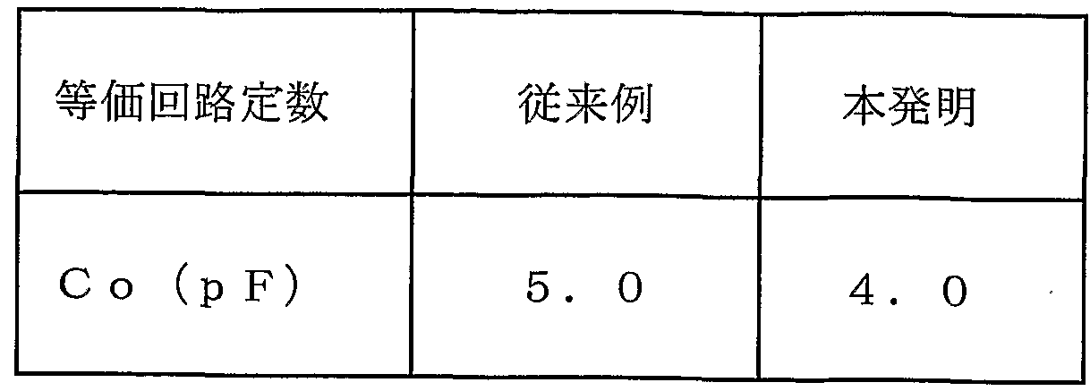
上表から本発明の圧電振動子の C oが減少していることが分かる。
なお、 前述の実施形態においては、 絶縁基板に、 A T水晶振動子を納めるため の凹部が形成されているが、 略平面状に絶縁基板を構成し、 絶縁基板上の A T水 晶振動子が載置される部分に配線を施すこともできる。 これによつて、 前述の実 施形態と同様の効果を奏することができる。 なお、 この場合、 A T水晶振動子を コンベックス型ではなく、 厚み一定の矩形 A T板とすることも好適である。
Claims
( 1 ) 第 1面に第 1励振電極が設けられ、 前記第 1面の裏側の面である第 2面 に第 2励振電極が設けられた圧電振動子と、
前記圧電振動子を載置する基板であって、 前記圧電振動子が載置された時に前 記第 1励振電極に接続される少なくとも一つの第 1接続電極と、 前記圧電振動子 が載置された時に前記第 2励振電極に接続される少なくとも一つの第 2接続電極 を有し、 前記圧電振動子の載置面に対して裏面側には少なくとも一つの第 1外部 電極と少なくとも一つの第 2外部電極を有し、 さらに、 前記第 1接続電極と前記 第 1外部電極を接続する第 1配線と、 前記第 2接続電極と前記第 2外部電極を接 続する第 2配線とを有するものであり、
前記圧電振動子が前記基板に載置された状態で、 前記基板の圧電振動子を載置 する面を覆い、 前記基板とともに前記圧電振動子を密封収容する蓋と、
を有し、
前記基板の、 圧電振動子の載置面と平行な平面に、 前記第 1および第 2外部電 極と、 前記第 1および第 2配線を投影した場合に、 第 1外部電極の影と第 2配線 の影、 第 2外部電極の影と第 1配線の影が重ならない、 圧電振動子ユニット。
( 2 ) 請求の範囲 (1 ) に記載の圧電振動子ユニットであって、
前記基板は、 前記圧電振動子が載置される載置面のほぼ中央部に前記圧電振動 子の少なくとも一部が納まる凹部を有する、 圧電振動子ュ-ット。
( 3 ) 請求の範囲 (2 ) に記載の圧電振動子ユニットであって、
前記基板は、 前記圧電振動子の載置面に平行な平面により第 1基板と第 2基板 に分割されており、
前記第 1基板は、 前記凹部に相当する貫通開口部と、 前記第 1および第 2接続 電極とを有し、 さらに、 前記第 1およぴ第 2接続電極の設けられた部分には、 当 該第 1基板を貫通する貫通孔を有するものであって、
前記第 2基板は、 前記第 1および第 2外部電極と、 前記第 1および第 2配線と、 前記第 1基板の貫通孔に対応する位置に設けられた貫通孔受けを有し、
さらに前記第 1および第 2配線の一部は、 前記凹部の底面に相当する部分に、
配置された、 圧電振動子ュ-ット。
( 4 ) 請求の範囲 (3 ) に記載の圧電振動子ユニットであって、
前記基板の外形は略方形であり、 前記凹部も略方形であり、
前記第 1およぴ第 2の接続電極は各々 2個であり、 前記略方形の凹部の四隅に、 略方形の短手方向の中心線に対し対称に配置され、
前記第 1およぴ第 2の外部電極は各々 2個であり、 前記略方形の基板の二つの 長辺にそれぞれ一つずつ長手方向の中心線に対し対称に配置される、
圧電振動子ュニット。
( 5 ) 請求の範囲 (3 ) に記載の圧電振動子ユニットであって、
前記第 1配線と第 1外部電極と第 1接続電極の総面積と、 前記第 2配線と第 2 外部電極と第 2接続電極の総面積とが等しい、 圧電振動子ュニット。
( 6 ) 請求の範囲 (5 ) に記載の圧電振動子ユニットであって、
前記第 1配線の面積と、 前記第 2配線の面積とが等しい、 圧電振動子ユニット c
( 7 ) 第 1面に第 1励振電極が設けられ、 前記第 1面の裏側の面である第 2面 に第 2励振電極が設けられた圧電振動子と、
前記圧電振動子を載置する基板であって、 当該基板は、 前記圧電振動子が載置 される載置面のほぼ中央部に前記圧電振動子の少なくとも一部が納まる凹部を有 し、 また前記圧電振動子が載置された時に前記第 1励振電極に接続される少なく とも一つの第 1接続電極と、 前記圧電振動子が載置された時に前記第 2励振電極 に接続される少なくとも一つの第 2接続電極を有し、 前記圧電振動子の載置面に 対して裏面側には少なくとも一つの第 1外部電極と少なくとも一つの第 2外部電 極を有し、 さらに、 前記第 1接続電極と前記第 1外部電極を接続する第 1配線と、 前記第 2接続電極と前記第 2外部電極を接続する第 2配線とを有するものであり、 前記圧電振動子が前記基板に載置された状態で、 前記基板の圧電振動子を載置 する面を覆い、 前記基板とともに前記圧電振動子を密封収容する蓋と、
を有し、
前記基板は、 前記圧電振動子の載置面に平行な平面により第 1基板と第 2基板 に分割されており、
前記第 1基板は、 前記凹部に相当する貫通開口部と、 前記第 1および第 2接続
電極とを有し、 さらに、 前記第 1およぴ第 2接続電極の設けられた部分には、 当 該第 1基板を貫通する貫通孔を有するものであって、
前記第 2基板は、 前記第 1および第 2外部電極と、 前記第 1およぴ第 2配線と. 前記第 1基板の貫通孔に対応する位置に設けられた貫通孔受けを有し、
前記第 1およぴ第 2配線の少なくとも一部は、 前記凹部の底面に相当する第 2 基板上の面に配置される、
圧電振動子ュニット。
( 8 ) 請求の範囲 (7 ) に記載の圧電振動子ユニットであって、
前記基板の外形は略方形であり、 前記凹部も略方形であり、
前記第 1および第 2の接続電極は各々 2個であり、 前記略方形の凹部の四隅に. 略方形の短軸方向の中心線に対し対称に配置され、
前記第 1および第 2の外部電極は各々 2個であり、 前記略方形の基板の二つの 長辺にそれぞれ一つずつ長手方向の中心線に対し対称に配置される、
圧電振動子ュニット。
( 9 ) 請求の範囲 (8 ) に記載の圧電振動子ユニットであって、
前記第 1および第 2配線は、 前記凹部の内部において、 当該凹部の長手方向の 中心線を横切らない、 圧電振動子ユニット。
Priority Applications (1)
| Application Number | Priority Date | Filing Date | Title |
|---|---|---|---|
| US08/860,630 US5982077A (en) | 1995-08-11 | 1996-11-07 | Piezo-electric transducer unit |
Applications Claiming Priority (2)
| Application Number | Priority Date | Filing Date | Title |
|---|---|---|---|
| JP7/316064 | 1995-11-08 | ||
| JP31606495A JP3924016B2 (ja) | 1995-11-08 | 1995-11-08 | 圧電振動子 |
Publications (1)
| Publication Number | Publication Date |
|---|---|
| WO2004100367A1 true WO2004100367A1 (ja) | 2004-11-18 |
Family
ID=18072868
Family Applications (1)
| Application Number | Title | Priority Date | Filing Date |
|---|---|---|---|
| PCT/JP1996/003263 Ceased WO2004100367A1 (ja) | 1995-08-11 | 1996-11-07 | 圧電振動子ユニット |
Country Status (3)
| Country | Link |
|---|---|
| US (1) | US5982077A (ja) |
| JP (1) | JP3924016B2 (ja) |
| WO (1) | WO2004100367A1 (ja) |
Families Citing this family (8)
| Publication number | Priority date | Publication date | Assignee | Title |
|---|---|---|---|---|
| US6396201B1 (en) | 1997-08-19 | 2002-05-28 | Miyota Co., Ltd. | Piezoelectric vibrator |
| US6229249B1 (en) * | 1998-08-31 | 2001-05-08 | Kyocera Corporation | Surface-mount type crystal oscillator |
| JP3770111B2 (ja) * | 2001-07-09 | 2006-04-26 | 株式会社村田製作所 | 圧電型電気音響変換器 |
| WO2005109638A1 (ja) * | 2004-05-12 | 2005-11-17 | Daishinku Corporation | 圧電振動素子用パッケージ及び圧電振動子 |
| KR101249312B1 (ko) * | 2005-09-30 | 2013-04-01 | 가부시키가이샤 다이신쿠 | 압전 진동 디바이스 |
| JP2012142700A (ja) * | 2010-12-28 | 2012-07-26 | Kyocera Crystal Device Corp | 圧電発振器 |
| JP2013165404A (ja) * | 2012-02-10 | 2013-08-22 | Seiko Instruments Inc | 振動デバイス及び発振器 |
| USD760230S1 (en) * | 2014-09-16 | 2016-06-28 | Daishinku Corporation | Piezoelectric vibration device |
Citations (3)
| Publication number | Priority date | Publication date | Assignee | Title |
|---|---|---|---|---|
| JPH03130618U (ja) * | 1990-04-11 | 1991-12-27 | ||
| JPH04298109A (ja) * | 1991-03-27 | 1992-10-21 | Seiko Epson Corp | 圧電振動子 |
| JPH07235854A (ja) * | 1994-02-23 | 1995-09-05 | Miyota Kk | 圧電振動子の容器 |
Family Cites Families (10)
| Publication number | Priority date | Publication date | Assignee | Title |
|---|---|---|---|---|
| EP0092428B1 (en) * | 1982-04-20 | 1990-04-04 | Fujitsu Limited | A method for producing a piezoelectric resonator |
| JPS59181713A (ja) * | 1983-03-30 | 1984-10-16 | Miyota Seimitsu Kk | 矩形状厚みすべり振動子の支持構造 |
| EP0127442B1 (en) * | 1983-05-30 | 1991-04-17 | Fujitsu Limited | Piezoelectric resonator |
| JPH03130618A (ja) * | 1989-10-16 | 1991-06-04 | Copal Co Ltd | 光学式変位検出装置 |
| JP2822846B2 (ja) * | 1992-10-29 | 1998-11-11 | 関西日本電気株式会社 | ガラス−セラミック複合体を用いた水晶振動子用フラットパッケージおよびこれを用いた水晶振動子 |
| US5585687A (en) * | 1994-02-23 | 1996-12-17 | Citizen Watch Co., Ltd. | Piezolelectric oscillator |
| JPH088682A (ja) * | 1994-06-17 | 1996-01-12 | Fujitsu Ltd | 直列共振デバイス及びその製造方法と試験方法 |
| JP3301262B2 (ja) * | 1995-03-28 | 2002-07-15 | 松下電器産業株式会社 | 弾性表面波装置 |
| JP3186510B2 (ja) * | 1995-06-09 | 2001-07-11 | 株式会社村田製作所 | 圧電共振部品及びその製造方法 |
| JPH09246904A (ja) * | 1996-03-14 | 1997-09-19 | Citizen Watch Co Ltd | 表面実装型水晶振動子 |
-
1995
- 1995-11-08 JP JP31606495A patent/JP3924016B2/ja not_active Expired - Fee Related
-
1996
- 1996-11-07 US US08/860,630 patent/US5982077A/en not_active Expired - Lifetime
- 1996-11-07 WO PCT/JP1996/003263 patent/WO2004100367A1/ja not_active Ceased
Patent Citations (3)
| Publication number | Priority date | Publication date | Assignee | Title |
|---|---|---|---|---|
| JPH03130618U (ja) * | 1990-04-11 | 1991-12-27 | ||
| JPH04298109A (ja) * | 1991-03-27 | 1992-10-21 | Seiko Epson Corp | 圧電振動子 |
| JPH07235854A (ja) * | 1994-02-23 | 1995-09-05 | Miyota Kk | 圧電振動子の容器 |
Also Published As
| Publication number | Publication date |
|---|---|
| JPH09135141A (ja) | 1997-05-20 |
| JP3924016B2 (ja) | 2007-06-06 |
| US5982077A (en) | 1999-11-09 |
Similar Documents
| Publication | Publication Date | Title |
|---|---|---|
| JP3334669B2 (ja) | 圧電共振部品 | |
| JPH08288785A (ja) | 幅モードを利用した共振子及び共振部品 | |
| EP0829957B1 (en) | Piezoelectric resonator and electronic component using the same | |
| JPH05315885A (ja) | チップ型発振子およびこの発振子を用いた発振回路 | |
| JP3924016B2 (ja) | 圧電振動子 | |
| US6097134A (en) | Piezoelectric resonator and electronic component including same | |
| US6064142A (en) | Piezoelectric resonator and electronic component containing same | |
| JPS6194408A (ja) | セラミツクフイルタ | |
| US5932951A (en) | Piezoelectric resonator and electronic component containing same | |
| EP0907242A2 (en) | Piezoelectric Component | |
| JPH03196594A (ja) | 回路基板とそれを用いた実装構造 | |
| JP3271538B2 (ja) | 圧電共振子およびそれを用いた電子部品 | |
| JP2004193965A (ja) | 圧電発振器の構造 | |
| JP2557761Y2 (ja) | 表面実装型圧電振動子 | |
| US6376970B1 (en) | Piezoelectric resonator supporting structure and a piezoelectric component including the same | |
| JPH11112277A (ja) | 電子部品およびラダーフィルタ | |
| JP3262021B2 (ja) | 圧電共振子およびそれを用いた電子部品 | |
| JPH114137A (ja) | 圧電部品 | |
| JP2004281803A (ja) | 圧電デバイス用パッケージ及び圧電デバイス | |
| EP0907243A2 (en) | Electronic component and ladder filter | |
| JP2003124774A (ja) | チップ型圧電発振子 | |
| JP2001168679A (ja) | ラダーフィルタ | |
| JPH0389708A (ja) | 圧電共振子 | |
| JP2000101384A (ja) | 圧電共振子およびこの圧電共振子を用いた圧電部品 | |
| JPS6214512A (ja) | フイルタ |
Legal Events
| Date | Code | Title | Description |
|---|---|---|---|
| WWE | Wipo information: entry into national phase |
Ref document number: 08860630 Country of ref document: US |
|
| AK | Designated states |
Kind code of ref document: A1 Designated state(s): US |