WO2011155355A1 - 連結システム - Google Patents
連結システム Download PDFInfo
- Publication number
- WO2011155355A1 WO2011155355A1 PCT/JP2011/062331 JP2011062331W WO2011155355A1 WO 2011155355 A1 WO2011155355 A1 WO 2011155355A1 JP 2011062331 W JP2011062331 W JP 2011062331W WO 2011155355 A1 WO2011155355 A1 WO 2011155355A1
- Authority
- WO
- WIPO (PCT)
- Prior art keywords
- door
- transport container
- container
- main body
- chamber
- Prior art date
- Legal status (The legal status is an assumption and is not a legal conclusion. Google has not performed a legal analysis and makes no representation as to the accuracy of the status listed.)
- Ceased
Links
Images


Classifications
-
- H—ELECTRICITY
- H10—SEMICONDUCTOR DEVICES; ELECTRIC SOLID-STATE DEVICES NOT OTHERWISE PROVIDED FOR
- H10P—GENERIC PROCESSES OR APPARATUS FOR THE MANUFACTURE OR TREATMENT OF DEVICES COVERED BY CLASS H10
- H10P72/00—Handling or holding of wafers, substrates or devices during manufacture or treatment thereof
- H10P72/10—Handling or holding of wafers, substrates or devices during manufacture or treatment thereof using carriers specially adapted therefor, e.g. front opening unified pods [FOUP]
- H10P72/19—Handling or holding of wafers, substrates or devices during manufacture or treatment thereof using carriers specially adapted therefor, e.g. front opening unified pods [FOUP] closed carriers
- H10P72/1916—Handling or holding of wafers, substrates or devices during manufacture or treatment thereof using carriers specially adapted therefor, e.g. front opening unified pods [FOUP] closed carriers characterised by sealing arrangements
-
- H—ELECTRICITY
- H10—SEMICONDUCTOR DEVICES; ELECTRIC SOLID-STATE DEVICES NOT OTHERWISE PROVIDED FOR
- H10P—GENERIC PROCESSES OR APPARATUS FOR THE MANUFACTURE OR TREATMENT OF DEVICES COVERED BY CLASS H10
- H10P72/00—Handling or holding of wafers, substrates or devices during manufacture or treatment thereof
- H10P72/30—Handling or holding of wafers, substrates or devices during manufacture or treatment thereof for conveying, e.g. between different workstations
- H10P72/34—Handling or holding of wafers, substrates or devices during manufacture or treatment thereof for conveying, e.g. between different workstations the wafers being stored in a carrier, involving loading and unloading
- H10P72/3406—Handling or holding of wafers, substrates or devices during manufacture or treatment thereof for conveying, e.g. between different workstations the wafers being stored in a carrier, involving loading and unloading involving removal of lid, door or cover
-
- B—PERFORMING OPERATIONS; TRANSPORTING
- B65—CONVEYING; PACKING; STORING; HANDLING THIN OR FILAMENTARY MATERIAL
- B65D—CONTAINERS FOR STORAGE OR TRANSPORT OF ARTICLES OR MATERIALS, e.g. BAGS, BARRELS, BOTTLES, BOXES, CANS, CARTONS, CRATES, DRUMS, JARS, TANKS, HOPPERS, FORWARDING CONTAINERS; ACCESSORIES, CLOSURES, OR FITTINGS THEREFOR; PACKAGING ELEMENTS; PACKAGES
- B65D45/00—Clamping or other pressure-applying devices for securing or retaining closure members
- B65D45/02—Clamping or other pressure-applying devices for securing or retaining closure members for applying axial pressure to engage closure with sealing surface
-
- H—ELECTRICITY
- H10—SEMICONDUCTOR DEVICES; ELECTRIC SOLID-STATE DEVICES NOT OTHERWISE PROVIDED FOR
- H10P—GENERIC PROCESSES OR APPARATUS FOR THE MANUFACTURE OR TREATMENT OF DEVICES COVERED BY CLASS H10
- H10P72/00—Handling or holding of wafers, substrates or devices during manufacture or treatment thereof
- H10P72/10—Handling or holding of wafers, substrates or devices during manufacture or treatment thereof using carriers specially adapted therefor, e.g. front opening unified pods [FOUP]
- H10P72/19—Handling or holding of wafers, substrates or devices during manufacture or treatment thereof using carriers specially adapted therefor, e.g. front opening unified pods [FOUP] closed carriers
- H10P72/1902—Handling or holding of wafers, substrates or devices during manufacture or treatment thereof using carriers specially adapted therefor, e.g. front opening unified pods [FOUP] closed carriers specially adapted for a single substrate
-
- H—ELECTRICITY
- H10—SEMICONDUCTOR DEVICES; ELECTRIC SOLID-STATE DEVICES NOT OTHERWISE PROVIDED FOR
- H10P—GENERIC PROCESSES OR APPARATUS FOR THE MANUFACTURE OR TREATMENT OF DEVICES COVERED BY CLASS H10
- H10P72/00—Handling or holding of wafers, substrates or devices during manufacture or treatment thereof
- H10P72/10—Handling or holding of wafers, substrates or devices during manufacture or treatment thereof using carriers specially adapted therefor, e.g. front opening unified pods [FOUP]
- H10P72/19—Handling or holding of wafers, substrates or devices during manufacture or treatment thereof using carriers specially adapted therefor, e.g. front opening unified pods [FOUP] closed carriers
- H10P72/1918—Handling or holding of wafers, substrates or devices during manufacture or treatment thereof using carriers specially adapted therefor, e.g. front opening unified pods [FOUP] closed carriers characterised by coupling elements, kinematic members, handles or elements to be externally gripped
-
- H—ELECTRICITY
- H10—SEMICONDUCTOR DEVICES; ELECTRIC SOLID-STATE DEVICES NOT OTHERWISE PROVIDED FOR
- H10P—GENERIC PROCESSES OR APPARATUS FOR THE MANUFACTURE OR TREATMENT OF DEVICES COVERED BY CLASS H10
- H10P72/00—Handling or holding of wafers, substrates or devices during manufacture or treatment thereof
- H10P72/10—Handling or holding of wafers, substrates or devices during manufacture or treatment thereof using carriers specially adapted therefor, e.g. front opening unified pods [FOUP]
- H10P72/19—Handling or holding of wafers, substrates or devices during manufacture or treatment thereof using carriers specially adapted therefor, e.g. front opening unified pods [FOUP] closed carriers
- H10P72/1922—Handling or holding of wafers, substrates or devices during manufacture or treatment thereof using carriers specially adapted therefor, e.g. front opening unified pods [FOUP] closed carriers characterised by the construction of the closed carrier
-
- H—ELECTRICITY
- H10—SEMICONDUCTOR DEVICES; ELECTRIC SOLID-STATE DEVICES NOT OTHERWISE PROVIDED FOR
- H10P—GENERIC PROCESSES OR APPARATUS FOR THE MANUFACTURE OR TREATMENT OF DEVICES COVERED BY CLASS H10
- H10P72/00—Handling or holding of wafers, substrates or devices during manufacture or treatment thereof
- H10P72/10—Handling or holding of wafers, substrates or devices during manufacture or treatment thereof using carriers specially adapted therefor, e.g. front opening unified pods [FOUP]
- H10P72/19—Handling or holding of wafers, substrates or devices during manufacture or treatment thereof using carriers specially adapted therefor, e.g. front opening unified pods [FOUP] closed carriers
- H10P72/1924—Handling or holding of wafers, substrates or devices during manufacture or treatment thereof using carriers specially adapted therefor, e.g. front opening unified pods [FOUP] closed carriers characterised by atmosphere control
-
- H—ELECTRICITY
- H10—SEMICONDUCTOR DEVICES; ELECTRIC SOLID-STATE DEVICES NOT OTHERWISE PROVIDED FOR
- H10P—GENERIC PROCESSES OR APPARATUS FOR THE MANUFACTURE OR TREATMENT OF DEVICES COVERED BY CLASS H10
- H10P72/00—Handling or holding of wafers, substrates or devices during manufacture or treatment thereof
- H10P72/30—Handling or holding of wafers, substrates or devices during manufacture or treatment thereof for conveying, e.g. between different workstations
- H10P72/32—Handling or holding of wafers, substrates or devices during manufacture or treatment thereof for conveying, e.g. between different workstations between different workstations
- H10P72/3218—Conveying cassettes, containers or carriers
-
- H—ELECTRICITY
- H10—SEMICONDUCTOR DEVICES; ELECTRIC SOLID-STATE DEVICES NOT OTHERWISE PROVIDED FOR
- H10P—GENERIC PROCESSES OR APPARATUS FOR THE MANUFACTURE OR TREATMENT OF DEVICES COVERED BY CLASS H10
- H10P72/00—Handling or holding of wafers, substrates or devices during manufacture or treatment thereof
- H10P72/30—Handling or holding of wafers, substrates or devices during manufacture or treatment thereof for conveying, e.g. between different workstations
- H10P72/33—Handling or holding of wafers, substrates or devices during manufacture or treatment thereof for conveying, e.g. between different workstations into and out of processing chamber
- H10P72/3308—Vertical transfer of a single workpiece
-
- H—ELECTRICITY
- H10—SEMICONDUCTOR DEVICES; ELECTRIC SOLID-STATE DEVICES NOT OTHERWISE PROVIDED FOR
- H10P—GENERIC PROCESSES OR APPARATUS FOR THE MANUFACTURE OR TREATMENT OF DEVICES COVERED BY CLASS H10
- H10P72/00—Handling or holding of wafers, substrates or devices during manufacture or treatment thereof
- H10P72/30—Handling or holding of wafers, substrates or devices during manufacture or treatment thereof for conveying, e.g. between different workstations
- H10P72/34—Handling or holding of wafers, substrates or devices during manufacture or treatment thereof for conveying, e.g. between different workstations the wafers being stored in a carrier, involving loading and unloading
- H10P72/3408—Docking arrangements
Definitions
- the present invention relates to a method for manufacturing an industrial product such as an element or a precision instrument represented by a semiconductor device or a thin film display device that requires cleaning, a manufacturing apparatus for the manufacturing method, and a cleaning technology.
- a pre-process for manufacturing a semiconductor integrated circuit can be cited as the only example.
- a wafer which is a product
- a container is transported between independent manufacturing apparatuses.
- Each device is equipped with an anterior chamber.
- the wafer container is connected to the front chamber. In the connected state, the wafer can be exchanged between the container and the manufacturing apparatus with the performance of blocking the wafer atmosphere from the outside with a certain level of performance.
- Containers are required to be light and small, and to have a simple mechanism in order to ensure easy transport.
- some ideas are required for the container opening and closing method, particularly the door storage method when opening the container door.
- the method of storing the container door in the wafer container at the time of connection with the front chamber is contrary to this requirement because a storage space for the door is required. From this, the door of the wafer container has an appropriate connection structure that is housed in the front chamber.
- HP has obtained one patent (Patent Document 1) for a connection method that takes this point into consideration.
- the container 1 is composed of a container body 3 and a container door 4, and the front chamber 2 is composed of a front chamber body 5 and a front chamber door 6.
- the front chamber main body 5-the front chamber door 6 and (c) the container main body 3-the front chamber main body 5 are provided with seal portions at three locations, and the three subsystems are necessary for transporting while blocking the inside and outside.
- the patentability of the SMIF patent lies in the sandwich trapping of fine particles on the door surface by the two doors. However, sandwiched microparticles are not excluded from the site. In addition, no measures are taken against the danger of particulates spilling from the end face of the sandwiched door and contaminating the wafer.
- this patent structure since the structure of the front chamber and the wafer transfer container is not hermetically sealed, this patent structure has a function to completely prevent the entry of externally contaminated wafers into the front chamber and the wafer transfer container. Not done.
- the connecting part consists of four structures: a container, a container door, a front chamber, and a front door. Then, as shown in FIG. 1 (b), of these four structures, (a) container main body 3-container door 4, (b) front chamber main body 5-front chamber door 6, (c) A seal for sealing is provided between the four structures of the container body 3-the front chamber body 5 and (d) the container door 4-the front chamber door 6.
- the adverse effects include an increase in manufacturing cost, an increase in weight, generation of a new fine particle generation source, an increase in difficulty in cleaning containers, and the like.
- gas shut-off not at a practical level, but also particulate shut-off was incomplete.
- the need for improvements to control and eliminate the generation of fine particles found in the improved patents is that the SMIF method and the first four Asyst sealing methods themselves have incomplete particle blocking performance. This means that it is not the best hermetic connection system.
- FIMS Front-opening Interface Interface Mechanical Standard
- the wafers are stored in a cassette inside the container because they are vertically connected. After the two doors combined after the connection are stored in the interior, the cassette moves to the front chamber. On the other hand, in FIMS, the cassette is omitted, and after the two doors combined in the horizontal direction move into the front chamber and then move down in the vertical direction, the wafer in the container It is taken out directly into the front room using a wafer transfer robot in the room.
- the container in order to reduce the pressure fluctuations that occur in the local environment when opening and closing the connected container door and front chamber door, and the problem of particulate generation caused by the generation of airflow, and sealing
- the container is provided with a pressure relief hole that leads to the outside world for two reasons to prevent the container door from becoming negative pressure and difficult to open.
- the gas molecules have a structure that cannot have a blocking performance.
- a pressure relief hole is also installed in the FMS system container FOUP (Front Opening Unified Pod) for 300mm wafers.
- FMS system container FOUP Front Opening Unified Pod
- the FIMS system introduced as a global standard in all the latest 300mm wafer compatible semiconductor integrated circuit manufacturing factories has a gap, so that not only gas molecules but also fine particles can be completely blocked. do not have.
- a clean room should be unnecessary if it is a completely local clean production system in terms of shut-off performance.
- the SMIF system is still installed in the clean room. In other words, at present, it is necessary to double clean a clean room and a local clean. This increases the amount of capital investment, requires advanced management, and greatly increases manufacturing costs.
- Patent Documents 7 to 9 describe devices that open a pod by bringing the pod and the device into close contact with each other so that the pod door and the port door of the device face each other, and then moving the pod door and the port door.
- the space formed by the pod door and the device port door is merely replaced with nitrogen, and does not clean the surface of the member that defines the space. If it is a vacuum, it indicates that it does not function because of the pressure difference.
- Patent Document 10 describes a means for holding the cap in order to open the cap of the storage box by means of magnetism or vacuum force, but this is only a holding means, and the cap surface faces the cap. It does not clean the door surface of the device.
- the invention described in Patent Document 11 describes that the shutter and lid of the vacuum clean box and the shutter of the clean device are joined in an airtight manner, and after the sealed space is evacuated, the shutter lid and the shutter are opened separately. All such methods must be performed under vacuum, and it is assumed that the outer surfaces of all members are cleaned.
- the space formed by the lid of the exposure mask container and the lid of the apparatus is evacuated and then these lids are opened, but this method is used only for the vacuum apparatus, Moreover, it is merely a vacuum, not a cleaning.
- the present invention is a connection system comprising a transport container composed of a transport container main body and a transport container door, and a device having an apparatus main body and an apparatus door.
- the apparatus has a first seal structure that can be sealed by tight connection, the apparatus has a second seal structure that can be sealed by close connection of the apparatus main body and the apparatus door, and the transfer container and the apparatus are sealed together.
- It has a third seal structure that can be sealed by connection, and forms a non-divided connection chamber sealed by the third seal only when the transport container and the apparatus are combined, and the transport container door is separated from the transport container.
- the connection system has a structure that is separated and taken into the apparatus.
- connection chamber is provided with a clean gas injection hole and an exhaust hole, and a valve having a function of controlling the pressure in the connection chamber has a structure in which either of the holes or the connection chamber is directly connected to the transfer chamber.
- the exhaust in which the pressure in the connection chamber is made negative more than the outside and the atmosphere in the connection chamber can be replaced with an arbitrary gas is connected to the exhaust device or the negative pressure generator. You may make it have a suction hole connected with the hole and the gas supply apparatus.
- a V-shaped groove directed in three different directions is provided on the outer surface of the transport container door, and when the transport container door is closed to the transport container body, a positioning pin is provided on the transport container body around the transport container door, Furthermore, a slope is provided around the transport container door, and the transport container formed so as to face the slope provided inside the transport container body, and each of these V-shaped grooves, positioning pins, and slopes, respectively.
- An apparatus door and an apparatus main body having a structure that fits into the apparatus can also be adopted.
- the structure of the apparatus can be further simplified, and it corresponds to the front chamber by the close contact structure between the transfer container and the apparatus.
- the space can be formed by a simple mechanism that only seals a place where there are only three seal portions and a mechanism for cleaning.
- the air pressure inside the container, the space constituted by the three seals, and the inside of the apparatus can be made similar, there is no need to make the inside of the container the same air pressure as the outside air, and dust, dust, particles when opening and closing And the like can be prevented from entering the inside.
- the transfer container and the apparatus main body are connected in an airtight manner, and only two doors are required to move the contents between them.
- One is the door of the container, and the other is the door of the apparatus main body.
- These two doors have such a shape that a connection chamber can be formed only when the transfer container and the apparatus are connected in an airtight manner. Since the inner surface of the connecting chamber is originally the outer surface of the two doors, it is a surface that may have been contaminated by exposure to the external space.
- connection chamber when a connection chamber is formed and a cleaning mechanism for the inside of the connection chamber is provided, further cleanliness can be secured, and separation between the inside of the transfer container, the inside of the apparatus, and the internal space consisting of the connection chamber and the outside can be realized.
- the present invention is fixed to a conventional SMIF method or a device having only a very ambiguous method as to what kind of structure and cleaning method exist for a small connection chamber generated between the device and the transport container at the time of connection. This is different from the method that provides a front room.
- a fixed front chamber is not required, there is no need to provide a door provided between the front chamber and the processing chamber in the apparatus, and the number of necessary doors is one by the amount of the door. In addition to reducing this, it also solves the incomplete internal / external blocking performance of the conventional local clean production system.
- a connection chamber that is hermetically sealed from the outside is formed when the apparatus and the transport container are connected. For this purpose, the following three seal structures are provided.
- the transport container has a first seal structure (seal 1) that can be sealed by tightly connecting the transport container body and the transport container door.
- a known means such as a latch can be adopted as the mechanism used for the close connection.
- the apparatus has a second seal structure (seal 2) that can be sealed by tightly connecting the apparatus main body and the apparatus door.
- the transport container main body and the apparatus main body have a third seal structure (seal 3) that can be hermetically sealed by the hermetic connection between them.
- these sealing structures can employ known sealing means such as O-rings and gaskets.
- connection chamber generated at the time of connection forms a sealed chamber
- the environment such as pressure, fine particle concentration and gas concentration in the connection chamber
- the connection chamber is equipped with an input port and an output port for the purpose of gas input / output or pressure control.
- the container door and the front chamber door need not be combined to capture and store the fine particles.
- this structure the function of completely blocking the outside and the product space from each other can be obtained for both fine particles and gas molecules, so this structure is called a clean-airtight coupling (Particle-Lock Airtight Docking: PLAD) structure. To do.
- the wall forming the connecting chamber formed when the apparatus and the transport container are combined is constituted by a part of each of the transport container main body, the transport container door, the apparatus main body, and the apparatus door.
- the surface of the portion that becomes the inner wall is in contact with the outer space, and the contaminants and gas molecules in the outer space are adhered and contaminated.
- the surfaces exposed to these external spaces are still contaminated, even when they form the internal walls of the connecting chamber when combined.
- the adhesion contamination of the inner wall of the connection chamber is caused by discharging the clean gas from the clean gas introduction port provided in the connection chamber so that the fine particles adhering to the wall are desorbed from the surface by the wind of the gas, and exhausted. Can be discharged from the port.
- gas molecules chemically adsorbed on the surface can also be desorbed from the surface by substituting with clean gas.
- the seal 1 and the seal 2 are released, that is, the transfer container door and the apparatus door are opened toward the inside of the apparatus, so that the space in the transfer container and the apparatus is integrated. Can be conveyed between the two.
- the seal 1 and the seal 2 are released, that is, the transfer container door and the apparatus door are opened toward the inside of the apparatus, so that the space in the transfer container and the apparatus is integrated. Can be conveyed between the two.
- some fine particles and gas molecules are generated from the portions where the seal portion and the two doors face the conveyance container and the member of the apparatus. There is.
- these generated contaminants enter the transfer container and the apparatus, they cause contamination of the object to be transferred. Therefore, it is necessary to devise a way for the contaminants generated in the seal portion to move to the connection chamber side.
- connection chamber The movement of the pollutant into the connection chamber is made possible by setting the pressure in the connection chamber to be lower than both the pressure inside the transfer container and inside the apparatus. This is because the substance flows to the lower pressure side. The contaminant sucked into the connection chamber is discharged to the outside through the exhaust hole. It is only possible to eliminate contaminants generated in such a connecting portion by providing a connecting chamber. However, if the pressure in the connection chamber has a certain pressure difference with respect to the pressure inside the transfer container or inside the apparatus, it may be difficult to open the transfer container door or the apparatus door against the pressure difference. There is sex.
- the temporarily formed connecting chamber can be evacuated. Therefore, even when the apparatus main body and the inside of the transport container are at a vacuum pressure, the door can be opened with almost no pressure difference between both sides of the door by evacuating the connection chamber.
- the vacuum device body is often kept in a vacuum at all times in order to avoid the time for returning the vacuum of the vacuum device body to the atmosphere and the resulting contamination.
- a vacuum chamber is usually provided with a front chamber. This anterior chamber goes back and forth between atmosphere and vacuum. For this reason, this front room may be called an air-lock room.
- the connecting chamber plays the role of this air-lock, that is, between the atmosphere and the vacuum
- the conventional fixed front chamber is not required.
- the front chamber itself has a door and a transport mechanism
- the volume of the front chamber is relatively large. For this reason, it takes a considerable time to exhaust the front chamber.
- the connecting chamber needs only a small space that can be formed when the container and the apparatus are united, it does not take much time to clean the connecting chamber itself when it is connected. Just do it.
- provision of the anterior chamber is not excluded.
- connection chamber When the contamination of the product with fine particles becomes a problem, it is particularly necessary to clean the connection chamber. On the other hand, if particulate contamination is not a problem and gas molecular contamination is a problem, the gas introduction and gas exhaust ports in the connection chamber may be omitted if the influence of the contamination is relatively insignificant. . Since the volume of the connection chamber is extremely small compared to the conventional front chamber, the absolute amount of pollutants inside it is also small, and if it diffuses into the volume of the transfer container and the manufacturing equipment, it is diluted For example, the density decreases by 4 digits or more. In applications where there is no problem with this dilute contamination concentration, there is no need to evacuate the connection chamber for cleaning or to install a port for introducing clean gas.
- the door of the transport container has a structure that opens to the inside of the apparatus after combining with the apparatus. If the container door is opened to the outside of the container before uniting, another door is required to prevent the inside of the container from being exposed to the outside, which is disadvantageous in terms of space saving and mechanism efficiency. .
- the volume used for moving the door of the transport container increases as it is pulled in the back direction, which is not desirable because the container to be transported becomes larger. Therefore, the door of the transport container is stored inside the apparatus.
- the transport container door is separately stored in the apparatus main body.
- the seal 1 that seals the transport container door and the transport container body is located between the transport container door and the transport container body.
- a magnetic hook mechanism may be used as a mechanism for suppressing generation of both fine particles and gas molecules.
- a mechanical key mechanism that has many sliding parts that are generally used, a large amount of fine particles are generated by sliding that occurs during opening and closing. Therefore, it should not be used when a high degree of cleaning is required.
- the present invention that does not have a sliding mechanism is suitable for high-level cleaning, but the opening / closing mechanism using magnetism does not involve such mechanical operation and does not generate sliding, so it is suitable for high-level cleaning. ing.
- a magnetic body (at least one of which is a magnet) may be provided on the transport container main body and the transport container door, and the transport container door and the transport container may be closed by an attractive force between the magnetic bodies.
- the transfer container door may be opened by incorporating a magnet into the apparatus door and attracting the transfer container door to the apparatus door by its magnetic force.
- Such a magnetic opening / closing mechanism is superior to the mechanical opening / closing mechanism in terms of cleaning, but the magnetic opening / closing mechanism is insufficient as an actual opening / closing mechanism of the transport container.
- the magnetic force strongly depends on the distance between the magnetic materials, and the strength increases rapidly when the attractive force is 1mm or less. On the other hand, it rapidly weakens when the distance exceeds that, so high accuracy is required for the product structure. This is one of the reasons. In particular, when the magnetic materials are brought into contact with each other, when viewed on a micron scale, the surface of the magnetic material is uneven, and if the accuracy does not reach the micron order, the magnetic attractive force is not intended. In addition, when there are a lot of the same items such as transport containers, the individual magnetic containers have slightly different dimensions, so that the magnetic attractive force may be different among the individual containers. In order to avoid the above problem, a structure that can control the distance between the magnetic bodies can be employed.
- the change in attractive force at a micron-scale distance where two magnetic bodies are in contact with each other is drastic, it is an object to avoid such a proximity distance from being used practically. If the distance is designed to be several tens of microns apart, the difference in suction force with an accuracy error of 10 ⁇ m is relatively small. Furthermore, in order to compensate for this reduced difference in attractive force, the magnetic force of the opening mechanism on the apparatus side is determined based on the magnetic force expected to be the weakest attractive force.
- the transport container in the present invention is a hermetically sealed container for transporting an object that causes some trouble such as contamination or reaction by directly touching the outside air.
- This "thing” includes semiconductor substrates, sensor substrates, microorganisms, culture media, genes, unstable compounds, metals that are easily oxidized, toxic substances, etc.
- Substances to be used in various applications such as substances that should be treated and substances that are highly reactive, and those that should be handled in devices such as clean rooms and glove boxes are now widely covered. Among them, widely used applications are semiconductor wafers with various diameters ranging from half-inch during processing to large diameters such as 450 mm, and transportation of semiconductor chips.
- the material and characteristics of the main body and door of the transport container can be selected.
- the size of the transfer container is determined in relation to the size of the object to be transferred, and it is also possible to provide a plurality of chambers for storing a plurality of objects in one transfer container.
- one door is provided on each of the front and back surfaces of one transport container, and an independent chamber is provided therein, or a plurality of doors are provided adjacent to each other on the surface of the disk-shaped transport container, The door can be provided with a corresponding chamber.
- a mechanism for locking the door so that the door does not open carelessly when the transport container is used alone as a container, such as during the transport of the transport container, and the lock is a transport container It is preferable from the viewpoint of usability to provide a mechanism that is automatically released when the apparatus is closely connected.
- the transport container If the item stored in the transport container moves carelessly, it becomes difficult to open the door of the transport container and introduce it into the device, or the stored item itself is likely to be damaged. In the transport container, it is necessary to provide some means such as a pressing member for fixing the stored item.
- an inclined portion extending to the side surface of the transport container is provided at the peripheral edge of the door side surface of the transport container body.
- This inclined portion is provided at the peripheral edge portion of the port of the apparatus main body, and coincides with the inclined portion provided toward the center of the port.
- the transport container main body around the transport container door is provided with a plurality of protrusions, and the protrusions are fitted into recesses provided in the port of the apparatus main body.
- three tips are provided as hemispherical protrusions on the outer surface of the door of the transport container, and three V-shaped grooves are provided radially on the surface of the apparatus door corresponding to the protrusions.
- the transport container is connected to the apparatus door with high accuracy as follows. First, the transport container approaching the apparatus main body is inserted so that the inclined portion provided at the peripheral edge portion of the door-side surface of the above-described transport container main body is aligned with the inclined portion provided at the peripheral edge portion of the port of the apparatus main body. start. Inserted halfway, the transport container is positioned to some extent with respect to the apparatus body. Next, the plurality of protrusions provided on the transfer container main body around the door of the transfer container are fitted into the corresponding recesses provided in the port of the apparatus main body.
- the device closely connected to the transport container may be various devices that handle the “object” transported as described above.
- the “object” is a semiconductor substrate, it may be a semiconductor manufacturing device or a sensor substrate.
- a device for sensor production a culture device or an analysis device for microorganisms, culture media, or genes, a reaction device or an analysis device for unstable compounds or oxidizable metals, and an analysis device for harmful substances.
- Various known devices that need to be operated with the outside air shut off, such as devices to be handled, can be selected.
- the semiconductor manufacturing apparatus a series of various apparatuses used in the semiconductor manufacturing process can be adopted.
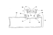
- FIG. 1C is a view in which the transport container 7 and the apparatus 8 constituting the connection system of the present invention are in close contact with each other.
- the transport container 7 is fixed to the apparatus 8 and is well known for close contact. Based on this means, the transport container 7 and the apparatus 8 are in close contact.
- the most characteristic point of the present invention is that the transport container 7 is not in close contact with the front chamber of the apparatus 8 but can be in close contact with the apparatus 8 itself. However, this does not exclude that the transport container 7 is in close contact with the front chamber of the apparatus.
- connection chamber 10 defined by the container door 12 of the transfer container 7 and the apparatus door 9 of the apparatus 8 serves as a front chamber in the conventional connection system. Formed as a thing.
- the front chamber in the prior art functions to connect the inside of the apparatus and the outside air having different environments, such as the atmosphere and a reduced pressure, or the atmosphere and a specific atmosphere, in order to carry the articles stored in the transport container into the apparatus.
- the connection chamber 10 in the present invention is as if it is the front chamber, and the environment inside the connection chamber 10 is the same as that of the outside immediately after the close connection. It moves toward the inside of the apparatus as a unit, and the same atmosphere as the inside of the apparatus via the gas supply port 15 and the gas discharge port 16 connected to the connection chamber until the two doors are opened. It can be adjusted to be an atmosphere.
- connection system of the present invention is required for each device used in each step. If the atmosphere in the apparatus is vacuum, the gas in the connection chamber 10 is discharged from the gas discharge port 16 by a vacuum pump or the like. If necessary, an inert gas is subsequently discharged from the gas supply port 15 in the connection chamber. After the introduction, the environment in the connection chamber 10 containing fine particles and the like is made to be similar to the environment in the apparatus by performing an operation of discharging the gas from the gas discharge port 16 an arbitrary number of times. It is possible.
- connection chamber 10 formed by the close connection includes a gas introduction port 15 and a gas discharge port.
- the device 8 can be provided with these ports so that 16 can be connected.
- the gas In order to clean the gas through the connection chamber 10 through these ports, it is necessary for the gas to flow through the entire connection chamber 10, and the container door 12 and the apparatus door 9 are in close contact with each other. It is also necessary for gas to circulate so that particles and the like attached to the opening 7 and the opening of the apparatus main body 8 can be removed.
- the transport container 7 includes a transport container main body 11 and a container door 12, and the transport container main body 11 and the container door are hermetically sealed by a known sealing means.
- the transfer container body 11 is provided with a member that supports the wafer 17 provided from the container door toward the inside of the transfer container body 11.
- the transport container 7 is provided with a magnet 18 on the wall portion of the transport container main body 11, and at a location where the container door 12 contacts the wall portion of the transport container main body 11.
- a magnetic material 19 such as iron can be provided.
- the wall portion of the transport container body 11 and the location where the magnetic body 19 of the container door 12 is provided are extended, and the location of the apparatus door 9 which contacts the location where the magnetic body 19 of the container door 12 is provided.
- the transport container main body 11 is firmly in close contact with the container door 12 by the magnetic force in the transport container 7, and the inside of the transport container main body 11 is reliably cut off from the outside air. Further, the device door 9 of the device 8 is in close contact with the device main body 13 by some means, and the device main body 13 is also in a state of being surely blocked from the outside air.
- the transport container 7 is a device of the device 8 in which the device door 9 is provided on the upper surface with the container door 12 facing downward. It is placed so as to be superimposed on the door 9.
- a positioning pin is provided in one of the transport container 7 and the apparatus 8 and a hole for fitting the positioning pin is provided in the other so that the transport container 7 and the apparatus 8 are accurately overlapped. It is important to.
- the positioning mechanism is not limited to the pin, and a known positioning means can be employed.
- the apparatus main body 13 and the apparatus door 9 are also hermetically sealed by known sealing means. After placing the transport container 7 on the apparatus 8 at an accurate position, an operation for tightly connecting the two is performed. When the tight connection is not performed, the transport container 7 and the device 8 are not hermetically sealed, and a gap is formed between them. When the door is opened in this state, outside air is transferred into the transport container 7 and the device. 8 enters and is contaminated with outside air and fine particles.
- a known means such as a latch mechanism may be used.
- sealing by a known sealing means such as a gasket interposed between the transport container main body 11 and the apparatus main body 13 is effective. It should be strong enough to function.
- an airtight seal structure is formed between the transport container main body 11 and the apparatus main body 13 by known sealing means provided on either one or both.
- a gas supply port 15 provided in the device in advance and The environment in the connection chamber 10 is adjusted using the port 16 for gas discharge.
- the air in the connection chamber 10 having the same environment as the outside air is exhausted from the gas discharge port 16 to reduce the pressure.
- a dry nitrogen gas is introduced from the gas supply port 15 and then exhausted from the gas discharge port 16 to reduce the pressure.
- the connection chamber 10 which is initially in the same environment as the outside air and contains contaminants such as fine particles in addition to the reactive gas such as oxygen is removed by the air flow due to the exhaust and supply of the gas.
- the fine particles that can be removed are removed, and the reactive gas such as oxygen is exhausted.
- the connecting chamber 10 is also under reduced pressure, and if the inside of the apparatus 8 is under an inert gas atmosphere, the connecting chamber 10 is also inactive.
- the gas atmosphere is adjusted.
- the environment of the connection chamber 10 may be adjusted by other processes.
- connection chamber 10 is not particularly different from the adjustment made in the front chamber in the conventional apparatus
- connection chamber defined by the doors of both the transfer container 7 and the apparatus 8 is conventionally used. Since it is overwhelmingly small compared to the front chamber, a smaller apparatus is sufficient for supplying and exhausting gas, and the required time is much shorter.
- an apparatus such as an elevator for opening and closing the apparatus door 9 is provided in the apparatus 8, and the wafer fixed to the container door of the transfer container 7 is transferred together with the container door 12 and the apparatus door 9. 8 to be processed by the processing means in the apparatus.
- the integrated container door 12 and apparatus door 9 are both moved into the apparatus 8, the close contact between the container door 12 and the container body 7 is released by a known means.
- the magnetic body 19 provided on the container door 12 is magnetically attached to the magnet 18 by receiving the magnetic force of the magnet 18 provided on the wall of the transport container body 7. For this reason, in order to separate the container door 12 from the transport container body 11, a force is exerted in a direction in which the container door 12 is separated from the magnetic body 19 against the magnetic force from the magnet 18 acting on the magnetic body 19. It is necessary to add.
- connection chamber 10 composed of the device door 9 and the container door 12 communicates with the space in the device 8, but since the connection chamber 10 is already in the same environment as the environment in the device 8, it is derived from the connection chamber 10. There is no contamination inside the device.
- this example is an example in which the gas supply port 15 and the gas discharge port 16 are provided in the apparatus 8, but these ports may not be provided. That is, when the volume of the device 8 and the volume of the connection chamber 10 are compared, the internal volume of the connection chamber 10 is overwhelmingly small, so even if fine particles or gas present in the connection chamber 10 are mixed into the atmosphere in the device, This is the case where the degree of contamination is extremely small and can be ignored.
- connection chamber 10 and the apparatus 8 in order to make the environment such as the atmospheric pressure in the connection chamber 10 and the device 8 formed the same, for example, an openable / closable pipe line that communicates the inside of the device 8 and the connection chamber 10 is provided in the device door 9 and transported. After the container 7 and the apparatus 8 are brought into close contact with each other and the connection chamber 10 is formed, the connection chamber 10 and the apparatus 8 may be communicated with each other by opening the pipe line. Furthermore, the direction of the apparatus door of the apparatus 8 of the above embodiment can be set sideways or downward, and the container door 12 of the transfer container 7 can also be set sideways or upward.
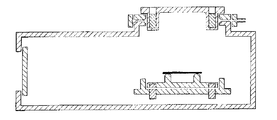
- FIG. 5 is a diagram showing a state in which the transport container 21 is in close contact with the apparatus 20.
- the container door 23 faces the upper surface of the apparatus door 22, and the portion around the container door 23 of the transport container body 25 faces the apparatus body 24.
- An electromagnet 26 is embedded in the device door, and its tip is exposed on the upper surface of the device door.
- a magnetic body 27 is embedded so as to penetrate the opposite surface from the surface of the container door 23 so as to face the position of the tip of the electromagnet 26.
- a plurality of the magnetic bodies 27 are embedded, and the plurality of magnetic bodies 27 are connected to both ends of the magnet 36 by a magnetic force. One or more pairs of such two magnetic bodies 27 and magnets 36 are embedded.
- the magnetic body 28 embedded in the transport container body 25 exerts a magnetic force on the inside of the container door 23, that is, the location where the magnetic body 27 is exposed on the transport container body side, and the container door 23 is embedded inside.
- the magnetic body 27 is fixed to the transport container body 25 by an attractive force generated by a magnetic force generated between the magnetic body 27 and the magnetic body 28 embedded in the transport container body 25. Is sealed.
- the plurality of magnetic bodies 28 embedded in the transport container body 25 are connected by a magnetic body 29 at a location away from the portion facing the container door 23. In this state, the transport container body and the container door are magnetically coupled. Are connected to form a closed circuit.
- An object to be processed 30 fixed to the container door 23 so as to be movable with the container door 23 between the apparatus 20 and the inside of the apparatus 20 is housed inside the transfer container body 25.
- the transfer container 21 and the apparatus 20 are in close contact to form a connection chamber,
- the connecting chamber needs to be airtight against the outside air.
- a seal member 31 such as an O-ring is provided to hermetically seal between the transfer container body 25 and the container door 23, and between the apparatus body 24 and the apparatus door 22.
- a sealing member 33 such as an O-ring for sealing is provided, and a sealing member 32 such as an O-ring for sealing the transfer container main body 25 and the apparatus main body 24 in an airtight manner is provided.
- the inside of the container 21 and the inside of the apparatus 20 can be kept in a state of being shielded from the outside air not only when the container 21 is connected to the apparatus 20 but also when it is not.
- the transport container main body 25 is provided.
- a positioning pin may be provided on the apparatus side and a hole or groove may be provided on the container side.
- a positioning pin is provided on the container side and the hole or groove is fitted to the positioning pin on the apparatus side. Is preferably formed.
- the tip shape of the positioning pin 34 may be spherical, conical, or pyramidal, as long as it has a clear tip as a pin.
- the hole or groove 35 may have an inner surface shape reflecting the shape of the tip of the positioning pin so as to be fitted to the positioning pin 34, but in particular, it is a V-shaped groove or a U-shaped groove. It is preferable.
- two points near the tip of the positioning pin 34 may be in contact with two points near the bottom of the hole or groove 35.
- the spherical portion at the tip of the positioning pin may be positioned at the center of the V-shaped groove 35, for example, when the tip of the positioning pin 34 is spherical and the hole or groove is a V-shaped groove. .
- the container 21 can be connected to the device 20 at a predetermined position accurately and reliably.
- the apparatus 20 is provided with a gas supply port and a gas discharge port as shown in FIG. 2, and the space between the transfer container body 25 and the apparatus body 24 is hermetically sealed by a seal member 32. Therefore, the connection chamber formed between the device door 22 and the container door 23 can be filled with an arbitrary gas so that it can be matched with the atmosphere in the device 20 or the container 21, or under an arbitrary pressure. It is also possible to do.
- the shape of the container, the device and their doors, the shape of the electromagnet, the shape of the magnetic body, the pin, hole, and groove are not limited to those shown in the figure, and any shape can be used as long as the same function can be exhibited. Can be used. Further, a magnet can be used instead of the electromagnet 26. Further, as shown in FIGS. 2 to 4, the apparatus shown in FIG. 5 is also configured such that the container door is moved into the apparatus together with the apparatus door, and predetermined processing is performed in the apparatus.
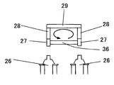
- FIG. 6 shows the relationship between each magnetic body and the electromagnet in the state shown in FIG. 5 and the state in which the transport container is positioned away from the apparatus.
- the transport container is located away from the electromagnet, and the electromagnet has no magnetic force.
- the transport container there are two magnetic bodies 27 connected by a magnet 36 embedded in the container door.
- Each of the magnetic bodies 27 is connected to a magnetic body 28 provided on the main body of the transport container, and these magnetic bodies 28 are further connected by a magnetic body 29.
- a circuit using magnetic force is formed in the direction of the arrow by each magnetic material as shown in FIG.
- FIG. 7 shows the relationship between the magnetic body and the electromagnet when the magnetic force is generated by the electromagnet 26 after the transport container is connected to the apparatus and the container door is not yet opened.
- the magnetic body 27 and the electromagnet 26 have a strong attractive force.
- the magnetic circuit constituted by the transfer container body 25 and the container door 23 has a considerably weak magnetic field line between the magnetic body 27 and the magnetic body 28 and is practically cut as a magnetic circuit. That is, the attractive force of the magnetic body 27 and the magnetic body 28 becomes extremely weak, and the magnetic lock of the transport container body 25 and the container door 23 is released.
- the magnetic lock between the transfer container body and the container door is released and the electromagnet and the container door are magnetically locked, so that the container door can be opened.
- the opening and closing of the container door and the opening and closing of the apparatus door can be performed simultaneously by the action of the electromagnet, so that outside air and external fine particles can be prevented from flowing into the container and the inside of the apparatus. Since a closed circuit of magnetic force is formed both before and after opening and closing, magnetic force does not leak to the outside.
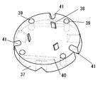
- FIG. 1 A schematic diagram of the structure seen from the inside of the transport container door is shown in FIG.
- the transport container door is closed so as to be embedded in the opening of the transport container, and has a disk shape having an inclined surface 37 that is not perpendicular to the upper and lower surfaces of the transport container door.
- Three claws 38 for holding the object to be conveyed are provided on the inner side. For example, a disk-shaped object to be conveyed is placed on these claws 38 or held by fitting.
- a groove 35 is provided on the outer surface of the transfer container door.
- a magnetic body 39 and a magnet 40 are embedded in the transport container door.
- FIGS. 1-10 A process of closing the transport container body 25 with the transport container door 23 will be described with reference to FIGS.
- the transport container door 23 is fitted into a transport container body 25 provided with a positioning pin for the apparatus, and the transported object is placed in the transport container.
- the transfer container door shown in FIG. 8 is inverted, and the inclined surface 37 of the transfer container door 23 is fitted to the inclined surface 43 inside the transfer container 25.
- the notch 41 provided around the transfer container door 23 is engaged with the protrusion 44 provided in the transfer container.
- an inclined surface 37 provided around the transfer container door and so as to coincide with the inclined surface 43 approaches the inclined surface 43 forming the inner surface of the transfer container body so as to gradually come into contact with the transferred container container.
- the transfer container door is fitted to the main body, the inclined surfaces 37 and 43 come into contact with each other.
- the magnetic body 39 of the transport container door 23 is disposed opposite to the magnetic body 42 provided in the transport container main body 25.
- the magnetic lines of the magnet 40 are directed to the magnetic body 42 via the magnetic body 39, so that the magnetic body 42 on the transport container body 25 side is attracted by the magnetic force to the magnetic body 39 on the transport container door side. Thereby, the transport container door 23 is fixed to the transport container body 25.
Landscapes
- Engineering & Computer Science (AREA)
- Mechanical Engineering (AREA)
- Container, Conveyance, Adherence, Positioning, Of Wafer (AREA)
Abstract
Description
巨大化が他産業に比較して特に進んでいることが理由で、清浄化のための手段としてクリーンルームを用いることが最適でないケミカルプラントを除き、先に例示した産業の製造工場の大半は、クリーンルームを用いた製造工程を有する。そこで、局所クリーン化生産方式等の手法によるクリーンルームのグレードダウン等によって、設備投資を削減する考え方が、即効的な手段として認識され始めた。一部の産業では実用化され普及が進みつつある。局所クリーン化には、工場の環境制御コストを削減する効果もある。
また、特許文献7~9には、ポッドと装置をポッドドアと装置のポートドアが対向するように密着させて、その後該ポッドドアとポートドアを移動させることによってポッドを開く装置が記載されているが、そのポッドドアと装置のポートドアにより形成される空間は単に窒素で置換するに留まるのであって、空間を規定する部材表面を清浄化するものではないし、窒素で置換することはポッドまたは装置内部が真空である場合には圧力差を理由に機能しないことを示す。
特許文献10には保管箱のキャップを開けるために、該キャップを保持する手段として磁気や真空力による手段が記載されているが、これはあくまで保持手段に過ぎず、該キャップ表面とそれに対向する装置の扉表面を清浄化させるものではない。
特許文献11記載の発明は真空クリーンボックスのシャッター兼用蓋体とクリーン装置のシャッターを気密に接合し、その密閉空間を真空にした後に該シャッター蓋体とシャッターを別々に開けることが記載されており、このような方法は全て真空下で行わなくてはならないし、全ての部材の外面を清浄化させておくことを前提としている。
特許文献12記載の発明は露光マスク容器の蓋と装置の蓋により形成される空間を真空にして、その後にこれらの蓋を開けるものであるが、この方法は真空装置にのみ使用されるし、しかも単に真空にするのみであって清浄化を行うものではない。
しかも容器蓋と装置扉等により形成される空間を単に真空にするのみでは清浄化できるとまではいえず、容器と装置間で摺擦する部位を排除することに加えて、該空間の雰囲気を置換する工程等を必要とする。
搬送容器扉外面には異なる3方向に向かうV字状の溝を設け、該搬送容器扉が搬送容器本体に閉じた状態において、該搬送容器扉の周囲の搬送容器本体には位置決めピンを設け、さらに、該搬送容器扉の周囲には斜面を設けて、搬送容器本体内部に設けた斜面を対向させるように設けてなる該搬送容器と、これらのV字状の溝、位置決めピン及び斜面のそれぞれに嵌合する構造を有する装置扉及び装置本体を採用することもできる。
また、容器内部、3つのシールにより構成される空間及び装置内部のそれぞれの気圧を同程度とすることができるので、容器内部を外気と同じ気圧にする必要がなく、開閉時に塵や埃、パーティクル等が内部に侵入することを防止できる。
2・・・従来の装置の前室
3・・・従来の搬送容器の本体
4・・・従来の搬送容器の容器扉
5・・・従来の装置の本体
6・・・従来の装置の装置扉
7・・・本発明における搬送容器
8・・・本発明における装置
9・・・装置扉
10・・連結室
11・・搬送容器本体
12・・搬送容器扉
13・・装置本体
14・・電磁石
15・・気体供給用ポート
16・・気体排出用ポート
17・・ウェハ
18・・永久磁石
19・・磁性体
20・・装置
21・・容器
22・・装置扉
23・・容器扉
24・・装置本体
25・・搬送容器本体
26・・電磁石
27・・磁性体
28・・磁性体
29・・磁性体
30・・被処理物
31・・シール部材
32・・シール部材
33・・シール部材
34・・位置決めピン
35・・溝
36・・磁石
37・・斜面
38・・爪
39・・磁性体
40・・磁石
41・・切り欠き部
42・・磁性体
43・・斜面
44・・突起
本発明では、搬送容器と装置本体を気密に連結し、これらの間で内容物を移動させるために必要な扉を2つだけとする。一つは容器の扉であり、もう一つは、装置本体の扉である。これらの2つの扉は、搬送容器と装置が気密に連結した時だけ連結室を形成できるような形状を有する。元々その連結室の内面は2つの扉の外面であるから、外部空間にさらされることで汚染された可能性がある表面である。従って、連結室を形成して連結室内部の清浄化機構を具備する場合には、さらに清浄性を確保でき、搬送容器内部、装置内部及び連結室からなる内部空間と外部との分離を実現できる。
本発明では、固定化された前室を要しないため、前室と装置内の処理室との間に設けられた扉を設ける必要はなく、その扉の分だけ、必要な扉の数を1つ減らすだけでなく、それと同時に従来の局所クリーン化生産システムの不完全な内外遮断性能を解決する。本発明においては、装置と搬送容器の連結時に、外部から密閉遮断される連結室を形成させる。そのために、以下の3つのシール構造を設ける。
次に、装置は、装置本体と装置扉の密着連結により密閉可能な第2番目のシール構造(シール2)を有する。最後に、搬送容器本体と装置本体は、両者の密閉連結により密閉可能な第3番目のシール構造(シール3)を有する。搬送容器と装置が連結する際には、最初の2つのシールに加えて、3番目のシールが成立するので、これらの3つのシールにより、分割されない1つの密閉化された連結室が形成される。
ここで、これらのシール構造は、Oリングやガスケット等の公知のシール手段を採用することが可能である。
また、連結室内の雰囲気を装置内部の雰囲気と同じ雰囲気に制御すると、搬送装置扉と装置扉を開ける前後において、装置内の雰囲気の組成が変化することがない。
ただし、連結室の気圧が、搬送容器内または装置内部の気圧に対してある程度の気圧差を有する場合には、その圧力差に抗して搬送容器扉や装置扉を開けることが困難になる可能性がある。
搬送容器の扉は装置との合体の後に装置内部に開かれる構造を有する。仮に、容器扉が容器の外へ合体前に開く方法では、容器内部が外部にさらされないよう、もう一つ扉が必要になってしまうので、省スペースとメカニズムの効率の点で、不利である。容器の内部へ搬送容器の扉が格納される方法では、奥方向へ引き込まれると、それだけ搬送容器の扉の移動に使う容積が増えてしまい、搬送する容器が大型化して望ましくない。従って、搬送容器の扉は装置内部へ格納される。
このような磁気開閉機構が機械開閉機構よりも清浄化の点で優れているが、磁気開閉機構は実際の搬送容器の開閉機構としては不十分な点がある。それは、磁気力が磁性体間の距離に強く依存しており、吸引力が1mm以下で急速に強くなって、逆にそれ以上の距離になると急速に弱くなるので、製品構造に高い精度を要求されることが理由の一つである。特に磁性体同士を接触させた場合、ミクロンスケールでみれば、磁性体表面は凹凸があり、精度もミクロンオーダに達していなければ、磁気吸引力は、意図したものにならない。また、搬送容器のように同じものがたくさんある場合、個々の容器で僅かに寸法が違うので、磁気吸引力が個々の容器で違う可能性がある。
以上の問題を回避するため、磁性体間の距離を制御できる構造を採用できる。2つの磁性体が接触しているミクロンスケールの距離での吸引力の変化が激しいので、そのような近接距離を、実用に用いないように回避することが目的である。数十ミクロン程度距離を離しておく設計とすると、10μmの精度誤差での吸引力の差は比較的小さくなる。さらに、この小さくなった吸引力の差を補うため、もっとも吸引力の弱くなると予想される磁気力を基準に、装置側の開放機構の磁気力を定める。
本発明における搬送容器は、外気に直接触れることにより汚染や反応等の何らかの支障を生じる物を搬送するための密閉容器である。この「物」としては、半導体用基板、センサ用基板、微生物、培地、遺伝子、不安定な化合物、酸化されやすい金属、有害物質等、化合物や菌等による汚染を避けるべき物質、拡散を防止すべき物質、反応性が高い物質等、各種用途に使用され、現在において、クリーンルームやグローブボックス等の装置内にて取り扱うべきものが広く対象となる。中でも広く使用される用途としては加工途中のハーフインチから450mm等の大口径に至る各種口径の半導体ウェハ、半導体チップの搬送等である。
搬送容器の扉側の面が装置扉に接続されるが、ここで搬送容器の扉が装置扉に対してずれることなく高精度に位置決めされることが必要である。この点は、搬送容器を手で装置扉に接続する場合であっても、あるいは搬送装置にて接続する場合であっても同じである。
しかも、搬送容器と装置扉との間で摺擦する部分があれば、その部分からはパーティクルを発生することになり、その後、装置内を汚染したり搬送容器内の物品を汚染することになりかねない。このため、搬送容器の扉側には特定の構造を持たせる必要がある。
まず、搬送容器の扉は、搬送容器本体に埋め込まれるようにして設置される。そして搬送容器本体の扉側の面の周縁部には搬送容器側面にかけての傾斜部を設ける。この傾斜部は装置本体のポートの周縁部に設け、ポート中心部に向けて設けられた傾斜部と一致するようにされている。
さらに搬送容器の扉の周囲の搬送容器本体部には、複数の突起部を設けてなり、該突起部は装置本体のポートに設けられた凹部に嵌合するようにされている。
さらに、搬送容器の扉の外面には3つの先端が半球状の突起として設けられ、この突起に対応して装置扉表面には3つのV字状の溝が放射状に設けられている。
このような構造の搬送容器本体、搬送容器扉、装置本体及び装置扉を使用して以下の通りに搬送容器は装置扉に高精度に接続される。
まず、装置本体に接近してきた搬送容器は、上記の搬送容器本体の扉側の面の周縁部に設けた傾斜部を装置本体のポートの周縁部に設けた傾斜部に合わせるようにして挿入され始める。途中まで挿入されて、搬送容器は装置本体に対して多少の遊びがある程度に位置決めされる。
次いで、上記の搬送容器の扉の周囲の搬送容器本体部に設けた複数の突起部が、対応する該装置本体のポートに設けられた凹部に嵌合する。この際に上記の多少の遊びは相当削減されて、搬送容器の垂直軸に対する回転がある程度抑制される。
その状態でさらに搬送容器本体が装置扉に接近すると、搬送容器の扉に設けた3つの先端の半球状の突起が、装置本体の扉に設けた上記の3つのV字の溝に入ることになる。このときには、1つのV字の溝を構成する対向した2つの斜面それぞれが、該半球状の突起と接触し、該半球状の突起は2箇所において該対向した2つの斜面それぞれと接触する。
この結果、搬送容器は垂直軸に対する回転方向へのぶれがなくなり、かつ水平方向へのぶれも放射状の3つのV字の溝により解消する。
このような機構によって、搬送容器は装置本体に対して垂直方向への移動以外は不可能となり固定される。
[装置]
上記搬送容器と密着連結される装置としては、上記のように搬送される「物」が取り扱われる各種装置でよく、「物」が半導体用基板であれば半導体製造用装置、センサ用基板であればセンサ製造用装置、微生物や培地、あるいは遺伝子であれば培養装置や分析装置、不安定な化合物や酸化されやすい金属であれば反応装置や分析装置、有害物質であれば分析装置等のそれを取り扱う装置等、外気を遮断して操作することが必要な公知の各種の装置を選択し得る。
なかでも半導体製造装置としては、半導体製造工程にて使用される一連の各種装置を採用することができる。
図1(c)は本発明の連結システムを構成する搬送容器7と装置8が密着連結している図であり、図示はしないが搬送容器7を装置8に固定し、密着連結させるための公知の手段に基づいて、搬送容器7と装置8が密着している。ここで、本発明の最も特徴的な点は、搬送容器7は装置8の前室に密着しているのではなく、装置8そのものに密着させることができる点である。ただし、これは搬送容器7が装置前室に密着することを排除するものではない。
前記のように、搬送容器7と装置8が密着連結した結果、搬送容器7の容器扉12と装置8の装置扉9で規定される連結室10が従来の連結システムにおける前室の役目を果たすものとして形成される。
装置内の雰囲気が真空であれば、気体排出用ポート16から連結室10内の気体を真空ポンプ等により排出し、必要であれば、続いて気体供給用ポート15から不活性の気体を連結室内に導入後、さらに気体排出用ポート16からその気体を排出する操作を任意の回数行う等により、微粒子等を含有している連結室10内の環境を装置内の環境と同程度のものとすることが可能である。
このように、本発明は搬送容器を前室ではなく直接装置8に密着連結できるものであり、そのために密着連結により形成された連結室10には、気体導入用ポート15及び気体排出用のポート16が接続されるように、装置8にはこれらのポートを設けることができる。
これらのポートにより連結室10内を気体が流通して清浄化するにあたっては、気体が連結室10内全てにわたって流通することが必要であるし、容器扉12と装置扉9が密着していた容器7の開口部及び装置本体8の開口部に付着している、粒子等も除去可能なように気体が流通することも必要である。
図2には、搬送容器7が搬送容器本体11と容器扉12からなり、搬送容器本体11と容器扉は公知のシール手段により気密にシールされている。そして搬送容器本体11には容器扉から搬送容器本体11の内部に向けて設けられたウェハ17を支持する部材を設けてなる。
搬送容器7を装置8の上に正確な位置で載置した後には、両者を密着連結させるための操作を行う。密着連結をしない場合には、搬送容器7と装置8が気密にシールされず、それらの間には隙間が形成されることになり、その状態で扉を開くと外気が搬送容器7内や装置8内に侵入し、これらの内部が外気と微粒子等で汚染されることになる。
この密着連結するための手段としては、ラッチ機構等の公知の手段でよく、その密着強度としては搬送容器本体11と装置本体13の間に介在するガスケット等の公知のシール手段によるシールが有効に機能する程度の強度でよい。
具体的な調整方法としては、当初は外気と同じ環境の連結室10内の空気を気体排出用ポート16から排気して減圧とする。次いで気体供給用ポート15から例えば乾燥した窒素ガスを導入し、さらに気体排出用ポート16から排気して減圧とする工程からなる方法を採用できる。
図示していないが、装置扉9を開閉するためのエレベータ等の装置が装置8内に設けられており、搬送容器7の容器扉に固定されたウェハを、容器扉12及び装置扉9ごと装置8内に移送して装置内の処理手段による処理に付すことになる。
一体化した容器扉12と装置扉9を共に装置8内に移動させるに際して、容器扉12と容器本体7との密着を公知の手段により解除する。
容器扉12に設けられた磁性体19は、搬送容器本体7の壁に設けられた磁石18の磁力を受けて、該磁石18と磁着している。
このため、容器扉12を搬送容器本体11から離すためには、磁性体19に作用する磁石18からの磁気力に抗して、磁性体19に対して容器扉12を離す方向へと力を加えることが必要である。
このように、装置扉9に容器扉12を磁着させた状態で、装置扉9を下方に移動させることにより、図4に示すように装置内に装置扉9と容器扉12が共に導入される。電磁石への通電は磁石18から容器扉12への磁気力がある程度弱くなった時点で停止してもよい。
この状態において、装置扉9と容器扉12からなる連結室10は装置8内の空間と連通するが、既に連結室10は装置8内の環境と同環境であるので、連結室10に由来する装置内の汚染はみられない。
さらに、上記の実施例の装置8の装置扉の向きを横向き、あるいは下向きとし、搬送容器7の容器扉12も横向き、あるいは上向きとすることも可能である。
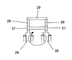
図5は搬送容器21が装置20に密着した状態の図であり、装置扉22の上面に容器扉23が対向し、搬送容器本体25の容器扉23の周囲の部分が装置本体24に対向している。
装置扉には、電磁石26が埋め込まれ、その先端が装置扉の上面に露出している。
該電磁石26の先端の位置に対向するように、磁性体27が容器扉23の表面から反対面を貫通するように埋め込まれている。この磁性体27は複数埋め込まれており、その複数の磁性体27は磁石36の両端に磁気力にて接続されている。そして、このような2つの磁性体27と磁石36からなる組が1つ以上埋め込まれている。
搬送容器本体25に埋め込まれた複数の磁性体28は、容器扉23と対向する部分から離れた箇所にて、磁性体29により接続されており、この状態において搬送容器本体と容器扉を磁気力が接続して閉回路が形成されている。
このため、図5においては搬送容器本体25と容器扉23との間を気密しシールするための、Oリング等のシール部材31が設けられ、装置本体24と装置扉22との間を気密にシールするための、Oリング等のシール部材33が設けられ、また搬送容器本体25と装置本体24を気密にシールするためのOリング等のシール部材32が設けられており、これらのシール部材により、容器21の内部と装置20の内部は、容器21が装置20に接続しているときはもちろん、そうでないときも、内部が外気から遮断された状態でいられることが可能である。
位置決めピン34の先端形状は円球状でも円錐状、角錐状でもよく、ピンとして明確な先端を備えるものであればよい。また穴や溝35はその位置決めピン34と嵌合するように、位置決めピンの先端形状を反映した内面の形状を有してもよいが、特にV字状の溝、U字状の溝とすることが好ましい。このときに位置決めピン34の先端付近の2点が穴や溝35の底部付近の2点に接触するようにしてもよい。このときには、例えば位置決めピン34の先端が円球状、穴や溝がV字の溝のときのように、位置決めピンの先端の円球状部分がV字の溝35の中心部に位置させてもよい。このような位置決め手段によれば、容器21を装置20に正確かつ確実に、予定した位置に接続させることが可能となる。
図5において、容器、装置及びそれらの扉の形状、電磁石の形状、磁性体の形状、ピンや穴、溝は図示されたものに限定されず、同様の機能を発揮可能であれば任意の形状のものでよい。また、電磁石26に代えて磁石とすることも可能である。
また、図2~4に示したように、図5に記載の装置も容器扉が装置扉と共に装置内に移動されて、装置内にて所定の処理等がなされるものである。
図6において、搬送容器は電磁石から離れた場所に位置し、電磁石は磁気力を持っていない状態にある。一方、搬送容器においては、容器扉に埋め込まれた磁石36により接続された2つの磁性体27がある。そして該磁性体27のそれぞれには搬送容器本体に設けられた磁性体28が接続され、さらにこれらの該磁性体28は磁性体29により接続されている。このように接続した結果、図6に示すようにそれぞれの磁性体により矢印方向に磁気力による回路が形成される。
まず電磁石26に電流を流して、電磁力を発生させると、その電磁力発生前に磁性体27内部で磁性体28へ向かっていた磁力線は、電磁石の磁力により、磁性体28へ向かうのをやめ、その磁力線は電磁石方向へ再配置される。結果として、磁石36-磁性体27-電磁石26-電磁石26-磁性体27という磁気回路を形成する。このことで、磁性体27と電磁石26は強い吸引力を持つことになる。このことで、搬送容器本体25と容器扉23で構成されていた磁気回路は、磁性体27と磁性体28の間で、磁力線がかなり弱くなり、事実上磁気回路として切断される。すなわち、磁性体27と磁性体28の吸引力が極めて弱くなり、搬送容器本体25と容器扉23は、磁気ロックが解除される。
以上のように、電磁石で磁力を発生させると、搬送容器本体と容器扉の磁気ロックが解除され、電磁石と容器扉が磁気ロックされるので、容器扉を開くことができることになる。
このように、電磁石の作用により容器扉の開閉と装置扉の開閉を同時に行うことができるので、外気や外部の微粒子が容器内部や装置内部に流入することを防止でき、その際には容器扉の開閉前後ともに磁気力の閉回路が形成されるので、磁気力が外部に漏れることがない。
この搬送容器扉には磁性体39及び磁石40が埋め込まれている。
該搬送容器扉23の爪38に被搬送物を保持した後に、装置との位置決めピンを備えた搬送容器本体25に搬送容器扉23を嵌合させるようにして該被搬送物を該搬送容器内に入れる。この際に、図8で示される搬送容器扉を反転し、該搬送容器扉23の斜面37を搬送容器25の内部の斜面43に合わせるようにして嵌合させる。このとき該搬送容器扉23の周囲に設けられた切り欠き部41が搬送容器内部に設けた突起44にかみ合うようにされる。さらに同時に該搬送容器扉の周囲に設けられ、かつ斜面43に一致するように設けられた斜面37が、該搬送容器本体の内面を形成する斜面43に徐々に接するように接近して該搬送容器本体に該搬送容器扉が嵌合されると同時に、該斜面37と43も接するようになる。
さらに、上記のように、該搬送容器扉23の磁性体39は、搬送容器本体25内部に設けた磁性体42と対向配置される。このとき、磁性体39を経由して磁石40の磁力線が磁性体42へ配向することで、該搬送容器扉側の磁性体39へ該搬送容器本体25側の磁性体42が磁気力で吸引され、これによって該搬送容器扉23は該搬送容器本体25に固定される。
Claims (5)
- 搬送容器本体と搬送容器扉で構成される搬送容器と、装置本体と装置扉を有する装置からなる連結システムであって、搬送容器は、搬送容器本体と搬送容器扉の密着連結により密閉可能な第1のシール構造を有し、装置は、装置本体と装置扉の密着連結により密閉可能な第2のシール構造を有し、さらに、搬送容器と装置は、両者が密着連結することにより形成される密閉可能な第3のシール構造を有し、搬送容器と装置が密着連結したときだけ、第3のシール構造によって密閉化された1つの分割されない連結室を形成し、さらに該連結室内を清浄化する手段を設けると共に、搬送容器扉が搬送容器から分離し装置内に取り込まれる構造を有する連結システム。
- 連結室には清浄気体噴入孔及び排気孔を有し、さらに連結室内の圧力制御を行う機能を有する弁がこれらの孔とその連結室のうちの1つ以上に直接接続されている構造を有する請求項1記載の連結システム。
- 搬送容器と装置の連結時には、連結室内の圧力を外部よりも負圧にすることが可能な、排気装置または負圧発生装置が連結された排気孔を有する請求項2記載の連結システム。
- 搬送容器扉外面には異なる3方向に向かうV字状の溝を設け、該搬送容器扉が搬送容器本体に閉じた状態において、搬送容器本体における該搬送容器扉の周囲に位置決めピンを設け、さらに、該搬送容器扉の周囲には斜面を設けてなる該搬送容器と、これらのV字状の溝、位置決めピン及び斜面のそれぞれに嵌合する構造を有する装置扉及び装置本体を採用する請求項1~3のいずれかに記載の連結システム。
- 搬送容器本体と搬送容器扉の密着連結により密閉可能なシール構造を有し、搬送容器扉外面には異なる3方向に向かうV字状の溝を設け、該搬送容器扉が搬送容器本体に閉じた状態において、該搬送容器扉の周囲の搬送容器本体には位置決めピンを設け、さらに、該搬送容器扉の周囲には斜面を設けて、搬送容器本体内部に設けた斜面を対向させるように設けてなる該搬送容器。
Priority Applications (5)
| Application Number | Priority Date | Filing Date | Title |
|---|---|---|---|
| KR1020127032456A KR101552383B1 (ko) | 2010-06-08 | 2011-05-30 | 연결 시스템 |
| CN201180028491.5A CN102934212B (zh) | 2010-06-08 | 2011-05-30 | 连结系统 |
| US13/702,493 US9281223B2 (en) | 2010-06-08 | 2011-05-30 | Coupling system |
| EP11792312.8A EP2581931B1 (en) | 2010-06-08 | 2011-05-30 | Connecting system |
| SG2012095253A SG186456A1 (en) | 2010-06-08 | 2011-05-30 | Coupling system |
Applications Claiming Priority (2)
| Application Number | Priority Date | Filing Date | Title |
|---|---|---|---|
| JP2010131470A JP5794497B2 (ja) | 2010-06-08 | 2010-06-08 | 連結システム |
| JP2010-131470 | 2010-06-08 |
Publications (1)
| Publication Number | Publication Date |
|---|---|
| WO2011155355A1 true WO2011155355A1 (ja) | 2011-12-15 |
Family
ID=45097963
Family Applications (1)
| Application Number | Title | Priority Date | Filing Date |
|---|---|---|---|
| PCT/JP2011/062331 Ceased WO2011155355A1 (ja) | 2010-06-08 | 2011-05-30 | 連結システム |
Country Status (8)
| Country | Link |
|---|---|
| US (1) | US9281223B2 (ja) |
| EP (1) | EP2581931B1 (ja) |
| JP (1) | JP5794497B2 (ja) |
| KR (1) | KR101552383B1 (ja) |
| CN (1) | CN102934212B (ja) |
| SG (2) | SG10201504168PA (ja) |
| TW (1) | TWI541931B (ja) |
| WO (1) | WO2011155355A1 (ja) |
Cited By (1)
| Publication number | Priority date | Publication date | Assignee | Title |
|---|---|---|---|---|
| US9016501B2 (en) | 2010-06-08 | 2015-04-28 | National Institute Of Advanced Industrial Science And Technology | Coupling transfer system |
Families Citing this family (245)
| Publication number | Priority date | Publication date | Assignee | Title |
|---|---|---|---|---|
| US20130023129A1 (en) | 2011-07-20 | 2013-01-24 | Asm America, Inc. | Pressure transmitter for a semiconductor processing environment |
| US20160376700A1 (en) | 2013-02-01 | 2016-12-29 | Asm Ip Holding B.V. | System for treatment of deposition reactor |
| US9016998B2 (en) * | 2013-03-14 | 2015-04-28 | Varian Semiconductor Equipment Associates, Inc. | High throughput, low volume clamshell load lock |
| US20150003826A1 (en) * | 2013-06-27 | 2015-01-01 | Success Prime Corporation | System and method for measuring differential mode delay |
| WO2015083679A1 (ja) | 2013-12-03 | 2015-06-11 | サンヨー株式会社 | フリーアクセス型の床構造、この床構造に対応する製造装置および運搬装置 |
| US20170234307A1 (en) * | 2014-03-02 | 2017-08-17 | Swissinnov Product Sarl | Volumetric pump with bleed mechanism |
| US10858737B2 (en) | 2014-07-28 | 2020-12-08 | Asm Ip Holding B.V. | Showerhead assembly and components thereof |
| US10941490B2 (en) | 2014-10-07 | 2021-03-09 | Asm Ip Holding B.V. | Multiple temperature range susceptor, assembly, reactor and system including the susceptor, and methods of using the same |
| JP6434050B2 (ja) | 2014-11-27 | 2018-12-05 | 国立研究開発法人産業技術総合研究所 | 前工程−後工程一体化システム |
| US10276355B2 (en) | 2015-03-12 | 2019-04-30 | Asm Ip Holding B.V. | Multi-zone reactor, system including the reactor, and method of using the same |
| US11139308B2 (en) | 2015-12-29 | 2021-10-05 | Asm Ip Holding B.V. | Atomic layer deposition of III-V compounds to form V-NAND devices |
| US10036197B1 (en) * | 2015-12-31 | 2018-07-31 | Vium, Inc. | Device, system and method of interconnecting doorways |
| US10529554B2 (en) | 2016-02-19 | 2020-01-07 | Asm Ip Holding B.V. | Method for forming silicon nitride film selectively on sidewalls or flat surfaces of trenches |
| US10343920B2 (en) | 2016-03-18 | 2019-07-09 | Asm Ip Holding B.V. | Aligned carbon nanotubes |
| US11453943B2 (en) | 2016-05-25 | 2022-09-27 | Asm Ip Holding B.V. | Method for forming carbon-containing silicon/metal oxide or nitride film by ALD using silicon precursor and hydrocarbon precursor |
| US9859151B1 (en) | 2016-07-08 | 2018-01-02 | Asm Ip Holding B.V. | Selective film deposition method to form air gaps |
| US10612137B2 (en) | 2016-07-08 | 2020-04-07 | Asm Ip Holdings B.V. | Organic reactants for atomic layer deposition |
| US9887082B1 (en) | 2016-07-28 | 2018-02-06 | Asm Ip Holding B.V. | Method and apparatus for filling a gap |
| US9812320B1 (en) | 2016-07-28 | 2017-11-07 | Asm Ip Holding B.V. | Method and apparatus for filling a gap |
| US11532757B2 (en) | 2016-10-27 | 2022-12-20 | Asm Ip Holding B.V. | Deposition of charge trapping layers |
| US10714350B2 (en) | 2016-11-01 | 2020-07-14 | ASM IP Holdings, B.V. | Methods for forming a transition metal niobium nitride film on a substrate by atomic layer deposition and related semiconductor device structures |
| KR102546317B1 (ko) | 2016-11-15 | 2023-06-21 | 에이에스엠 아이피 홀딩 비.브이. | 기체 공급 유닛 및 이를 포함하는 기판 처리 장치 |
| US11581186B2 (en) | 2016-12-15 | 2023-02-14 | Asm Ip Holding B.V. | Sequential infiltration synthesis apparatus |
| US11447861B2 (en) | 2016-12-15 | 2022-09-20 | Asm Ip Holding B.V. | Sequential infiltration synthesis apparatus and a method of forming a patterned structure |
| US11390950B2 (en) | 2017-01-10 | 2022-07-19 | Asm Ip Holding B.V. | Reactor system and method to reduce residue buildup during a film deposition process |
| US10468261B2 (en) | 2017-02-15 | 2019-11-05 | Asm Ip Holding B.V. | Methods for forming a metallic film on a substrate by cyclical deposition and related semiconductor device structures |
| US10770286B2 (en) | 2017-05-08 | 2020-09-08 | Asm Ip Holdings B.V. | Methods for selectively forming a silicon nitride film on a substrate and related semiconductor device structures |
| US12040200B2 (en) | 2017-06-20 | 2024-07-16 | Asm Ip Holding B.V. | Semiconductor processing apparatus and methods for calibrating a semiconductor processing apparatus |
| US11306395B2 (en) | 2017-06-28 | 2022-04-19 | Asm Ip Holding B.V. | Methods for depositing a transition metal nitride film on a substrate by atomic layer deposition and related deposition apparatus |
| KR20190009245A (ko) | 2017-07-18 | 2019-01-28 | 에이에스엠 아이피 홀딩 비.브이. | 반도체 소자 구조물 형성 방법 및 관련된 반도체 소자 구조물 |
| US11374112B2 (en) | 2017-07-19 | 2022-06-28 | Asm Ip Holding B.V. | Method for depositing a group IV semiconductor and related semiconductor device structures |
| US10590535B2 (en) | 2017-07-26 | 2020-03-17 | Asm Ip Holdings B.V. | Chemical treatment, deposition and/or infiltration apparatus and method for using the same |
| TWI815813B (zh) | 2017-08-04 | 2023-09-21 | 荷蘭商Asm智慧財產控股公司 | 用於分配反應腔內氣體的噴頭總成 |
| US10692741B2 (en) | 2017-08-08 | 2020-06-23 | Asm Ip Holdings B.V. | Radiation shield |
| US10770336B2 (en) | 2017-08-08 | 2020-09-08 | Asm Ip Holding B.V. | Substrate lift mechanism and reactor including same |
| US11769682B2 (en) | 2017-08-09 | 2023-09-26 | Asm Ip Holding B.V. | Storage apparatus for storing cassettes for substrates and processing apparatus equipped therewith |
| US11830730B2 (en) | 2017-08-29 | 2023-11-28 | Asm Ip Holding B.V. | Layer forming method and apparatus |
| US11295980B2 (en) | 2017-08-30 | 2022-04-05 | Asm Ip Holding B.V. | Methods for depositing a molybdenum metal film over a dielectric surface of a substrate by a cyclical deposition process and related semiconductor device structures |
| US10658205B2 (en) | 2017-09-28 | 2020-05-19 | Asm Ip Holdings B.V. | Chemical dispensing apparatus and methods for dispensing a chemical to a reaction chamber |
| US10403504B2 (en) | 2017-10-05 | 2019-09-03 | Asm Ip Holding B.V. | Method for selectively depositing a metallic film on a substrate |
| US10923344B2 (en) | 2017-10-30 | 2021-02-16 | Asm Ip Holding B.V. | Methods for forming a semiconductor structure and related semiconductor structures |
| KR102633318B1 (ko) | 2017-11-27 | 2024-02-05 | 에이에스엠 아이피 홀딩 비.브이. | 청정 소형 구역을 포함한 장치 |
| CN111316417B (zh) | 2017-11-27 | 2023-12-22 | 阿斯莫Ip控股公司 | 与批式炉偕同使用的用于储存晶圆匣的储存装置 |
| US10872771B2 (en) | 2018-01-16 | 2020-12-22 | Asm Ip Holding B. V. | Method for depositing a material film on a substrate within a reaction chamber by a cyclical deposition process and related device structures |
| TWI799494B (zh) | 2018-01-19 | 2023-04-21 | 荷蘭商Asm 智慧財產控股公司 | 沈積方法 |
| KR102695659B1 (ko) | 2018-01-19 | 2024-08-14 | 에이에스엠 아이피 홀딩 비.브이. | 플라즈마 보조 증착에 의해 갭 충진 층을 증착하는 방법 |
| US11081345B2 (en) | 2018-02-06 | 2021-08-03 | Asm Ip Holding B.V. | Method of post-deposition treatment for silicon oxide film |
| US10896820B2 (en) | 2018-02-14 | 2021-01-19 | Asm Ip Holding B.V. | Method for depositing a ruthenium-containing film on a substrate by a cyclical deposition process |
| US11685991B2 (en) | 2018-02-14 | 2023-06-27 | Asm Ip Holding B.V. | Method for depositing a ruthenium-containing film on a substrate by a cyclical deposition process |
| US10731249B2 (en) | 2018-02-15 | 2020-08-04 | Asm Ip Holding B.V. | Method of forming a transition metal containing film on a substrate by a cyclical deposition process, a method for supplying a transition metal halide compound to a reaction chamber, and related vapor deposition apparatus |
| KR102636427B1 (ko) | 2018-02-20 | 2024-02-13 | 에이에스엠 아이피 홀딩 비.브이. | 기판 처리 방법 및 장치 |
| US10975470B2 (en) | 2018-02-23 | 2021-04-13 | Asm Ip Holding B.V. | Apparatus for detecting or monitoring for a chemical precursor in a high temperature environment |
| US11473195B2 (en) | 2018-03-01 | 2022-10-18 | Asm Ip Holding B.V. | Semiconductor processing apparatus and a method for processing a substrate |
| KR102646467B1 (ko) | 2018-03-27 | 2024-03-11 | 에이에스엠 아이피 홀딩 비.브이. | 기판 상에 전극을 형성하는 방법 및 전극을 포함하는 반도체 소자 구조 |
| KR102600229B1 (ko) | 2018-04-09 | 2023-11-10 | 에이에스엠 아이피 홀딩 비.브이. | 기판 지지 장치, 이를 포함하는 기판 처리 장치 및 기판 처리 방법 |
| US12025484B2 (en) | 2018-05-08 | 2024-07-02 | Asm Ip Holding B.V. | Thin film forming method |
| US12272527B2 (en) | 2018-05-09 | 2025-04-08 | Asm Ip Holding B.V. | Apparatus for use with hydrogen radicals and method of using same |
| KR102596988B1 (ko) | 2018-05-28 | 2023-10-31 | 에이에스엠 아이피 홀딩 비.브이. | 기판 처리 방법 및 그에 의해 제조된 장치 |
| US11718913B2 (en) | 2018-06-04 | 2023-08-08 | Asm Ip Holding B.V. | Gas distribution system and reactor system including same |
| KR102568797B1 (ko) | 2018-06-21 | 2023-08-21 | 에이에스엠 아이피 홀딩 비.브이. | 기판 처리 시스템 |
| US10797133B2 (en) | 2018-06-21 | 2020-10-06 | Asm Ip Holding B.V. | Method for depositing a phosphorus doped silicon arsenide film and related semiconductor device structures |
| US11492703B2 (en) | 2018-06-27 | 2022-11-08 | Asm Ip Holding B.V. | Cyclic deposition methods for forming metal-containing material and films and structures including the metal-containing material |
| CN120591748A (zh) | 2018-06-27 | 2025-09-05 | Asm Ip私人控股有限公司 | 用于形成含金属的材料的循环沉积方法及膜和结构 |
| US10388513B1 (en) | 2018-07-03 | 2019-08-20 | Asm Ip Holding B.V. | Method for depositing silicon-free carbon-containing film as gap-fill layer by pulse plasma-assisted deposition |
| US10755922B2 (en) | 2018-07-03 | 2020-08-25 | Asm Ip Holding B.V. | Method for depositing silicon-free carbon-containing film as gap-fill layer by pulse plasma-assisted deposition |
| US11053591B2 (en) | 2018-08-06 | 2021-07-06 | Asm Ip Holding B.V. | Multi-port gas injection system and reactor system including same |
| US11430674B2 (en) | 2018-08-22 | 2022-08-30 | Asm Ip Holding B.V. | Sensor array, apparatus for dispensing a vapor phase reactant to a reaction chamber and related methods |
| KR102707956B1 (ko) | 2018-09-11 | 2024-09-19 | 에이에스엠 아이피 홀딩 비.브이. | 박막 증착 방법 |
| US11024523B2 (en) | 2018-09-11 | 2021-06-01 | Asm Ip Holding B.V. | Substrate processing apparatus and method |
| CN110970344B (zh) | 2018-10-01 | 2024-10-25 | Asmip控股有限公司 | 衬底保持设备、包含所述设备的系统及其使用方法 |
| KR102592699B1 (ko) | 2018-10-08 | 2023-10-23 | 에이에스엠 아이피 홀딩 비.브이. | 기판 지지 유닛 및 이를 포함하는 박막 증착 장치와 기판 처리 장치 |
| KR102546322B1 (ko) | 2018-10-19 | 2023-06-21 | 에이에스엠 아이피 홀딩 비.브이. | 기판 처리 장치 및 기판 처리 방법 |
| US12378665B2 (en) | 2018-10-26 | 2025-08-05 | Asm Ip Holding B.V. | High temperature coatings for a preclean and etch apparatus and related methods |
| US11087997B2 (en) | 2018-10-31 | 2021-08-10 | Asm Ip Holding B.V. | Substrate processing apparatus for processing substrates |
| KR102748291B1 (ko) | 2018-11-02 | 2024-12-31 | 에이에스엠 아이피 홀딩 비.브이. | 기판 지지 유닛 및 이를 포함하는 기판 처리 장치 |
| US11572620B2 (en) | 2018-11-06 | 2023-02-07 | Asm Ip Holding B.V. | Methods for selectively depositing an amorphous silicon film on a substrate |
| US10818758B2 (en) | 2018-11-16 | 2020-10-27 | Asm Ip Holding B.V. | Methods for forming a metal silicate film on a substrate in a reaction chamber and related semiconductor device structures |
| US12040199B2 (en) | 2018-11-28 | 2024-07-16 | Asm Ip Holding B.V. | Substrate processing apparatus for processing substrates |
| US11217444B2 (en) | 2018-11-30 | 2022-01-04 | Asm Ip Holding B.V. | Method for forming an ultraviolet radiation responsive metal oxide-containing film |
| KR102636428B1 (ko) | 2018-12-04 | 2024-02-13 | 에이에스엠 아이피 홀딩 비.브이. | 기판 처리 장치를 세정하는 방법 |
| US11158513B2 (en) | 2018-12-13 | 2021-10-26 | Asm Ip Holding B.V. | Methods for forming a rhenium-containing film on a substrate by a cyclical deposition process and related semiconductor device structures |
| JP7504584B2 (ja) | 2018-12-14 | 2024-06-24 | エーエスエム・アイピー・ホールディング・ベー・フェー | 窒化ガリウムの選択的堆積を用いてデバイス構造体を形成する方法及びそのためのシステム |
| TWI866480B (zh) | 2019-01-17 | 2024-12-11 | 荷蘭商Asm Ip 私人控股有限公司 | 藉由循環沈積製程於基板上形成含過渡金屬膜之方法 |
| TWI873122B (zh) | 2019-02-20 | 2025-02-21 | 荷蘭商Asm Ip私人控股有限公司 | 填充一基板之一表面內所形成的一凹槽的方法、根據其所形成之半導體結構、及半導體處理設備 |
| JP7509548B2 (ja) | 2019-02-20 | 2024-07-02 | エーエスエム・アイピー・ホールディング・ベー・フェー | 基材表面内に形成された凹部を充填するための周期的堆積方法および装置 |
| US11482533B2 (en) | 2019-02-20 | 2022-10-25 | Asm Ip Holding B.V. | Apparatus and methods for plug fill deposition in 3-D NAND applications |
| TWI842826B (zh) | 2019-02-22 | 2024-05-21 | 荷蘭商Asm Ip私人控股有限公司 | 基材處理設備及處理基材之方法 |
| US11469124B2 (en) * | 2019-03-05 | 2022-10-11 | Applied Materials, Inc. | Contactless latch and coupling for vacuum wafer transfer cassette |
| KR102858005B1 (ko) | 2019-03-08 | 2025-09-09 | 에이에스엠 아이피 홀딩 비.브이. | 실리콘 질화물 층을 선택적으로 증착하는 방법, 및 선택적으로 증착된 실리콘 질화물 층을 포함하는 구조체 |
| US11742198B2 (en) | 2019-03-08 | 2023-08-29 | Asm Ip Holding B.V. | Structure including SiOCN layer and method of forming same |
| KR20200116033A (ko) * | 2019-03-28 | 2020-10-08 | 에이에스엠 아이피 홀딩 비.브이. | 도어 개방기 및 이를 구비한 기판 처리 장치 |
| KR102809999B1 (ko) | 2019-04-01 | 2025-05-19 | 에이에스엠 아이피 홀딩 비.브이. | 반도체 소자를 제조하는 방법 |
| US11447864B2 (en) | 2019-04-19 | 2022-09-20 | Asm Ip Holding B.V. | Layer forming method and apparatus |
| KR20200125453A (ko) | 2019-04-24 | 2020-11-04 | 에이에스엠 아이피 홀딩 비.브이. | 기상 반응기 시스템 및 이를 사용하는 방법 |
| KR102929471B1 (ko) | 2019-05-07 | 2026-02-20 | 에이에스엠 아이피 홀딩 비.브이. | 딥 튜브가 있는 화학물질 공급원 용기 |
| KR102929472B1 (ko) | 2019-05-10 | 2026-02-20 | 에이에스엠 아이피 홀딩 비.브이. | 표면 상에 재료를 증착하는 방법 및 본 방법에 따라 형성된 구조 |
| JP7598201B2 (ja) | 2019-05-16 | 2024-12-11 | エーエスエム・アイピー・ホールディング・ベー・フェー | ウェハボートハンドリング装置、縦型バッチ炉および方法 |
| JP7612342B2 (ja) | 2019-05-16 | 2025-01-14 | エーエスエム・アイピー・ホールディング・ベー・フェー | ウェハボートハンドリング装置、縦型バッチ炉および方法 |
| USD975665S1 (en) | 2019-05-17 | 2023-01-17 | Asm Ip Holding B.V. | Susceptor shaft |
| USD947913S1 (en) | 2019-05-17 | 2022-04-05 | Asm Ip Holding B.V. | Susceptor shaft |
| KR20200141002A (ko) | 2019-06-06 | 2020-12-17 | 에이에스엠 아이피 홀딩 비.브이. | 배기 가스 분석을 포함한 기상 반응기 시스템을 사용하는 방법 |
| KR102918757B1 (ko) | 2019-06-10 | 2026-01-28 | 에이에스엠 아이피 홀딩 비.브이. | 석영 에피택셜 챔버를 세정하는 방법 |
| KR20200143254A (ko) | 2019-06-11 | 2020-12-23 | 에이에스엠 아이피 홀딩 비.브이. | 개질 가스를 사용하여 전자 구조를 형성하는 방법, 상기 방법을 수행하기 위한 시스템, 및 상기 방법을 사용하여 형성되는 구조 |
| KR102911421B1 (ko) | 2019-07-03 | 2026-01-12 | 에이에스엠 아이피 홀딩 비.브이. | 기판 처리 장치용 온도 제어 조립체 및 이를 사용하는 방법 |
| JP7499079B2 (ja) | 2019-07-09 | 2024-06-13 | エーエスエム・アイピー・ホールディング・ベー・フェー | 同軸導波管を用いたプラズマ装置、基板処理方法 |
| CN112216646B (zh) | 2019-07-10 | 2026-02-10 | Asmip私人控股有限公司 | 基板支撑组件及包括其的基板处理装置 |
| KR102895115B1 (ko) | 2019-07-16 | 2025-12-03 | 에이에스엠 아이피 홀딩 비.브이. | 기판 처리 장치 |
| TWI826704B (zh) | 2019-07-17 | 2023-12-21 | 荷蘭商Asm Ip私人控股有限公司 | 自由基輔助引燃電漿系統和方法 |
| KR102860110B1 (ko) | 2019-07-17 | 2025-09-16 | 에이에스엠 아이피 홀딩 비.브이. | 실리콘 게르마늄 구조를 형성하는 방법 |
| US11643724B2 (en) | 2019-07-18 | 2023-05-09 | Asm Ip Holding B.V. | Method of forming structures using a neutral beam |
| KR102903090B1 (ko) | 2019-07-19 | 2025-12-19 | 에이에스엠 아이피 홀딩 비.브이. | 토폴로지-제어된 비정질 탄소 중합체 막을 형성하는 방법 |
| CN112309843B (zh) | 2019-07-29 | 2026-01-23 | Asmip私人控股有限公司 | 实现高掺杂剂掺入的选择性沉积方法 |
| US12169361B2 (en) | 2019-07-30 | 2024-12-17 | Asm Ip Holding B.V. | Substrate processing apparatus and method |
| CN112309900B (zh) | 2019-07-30 | 2025-11-04 | Asmip私人控股有限公司 | 基板处理设备 |
| CN112309899B (zh) | 2019-07-30 | 2025-11-14 | Asmip私人控股有限公司 | 基板处理设备 |
| US11227782B2 (en) | 2019-07-31 | 2022-01-18 | Asm Ip Holding B.V. | Vertical batch furnace assembly |
| US11587815B2 (en) | 2019-07-31 | 2023-02-21 | Asm Ip Holding B.V. | Vertical batch furnace assembly |
| US11587814B2 (en) | 2019-07-31 | 2023-02-21 | Asm Ip Holding B.V. | Vertical batch furnace assembly |
| CN112323048B (zh) | 2019-08-05 | 2024-02-09 | Asm Ip私人控股有限公司 | 用于化学源容器的液位传感器 |
| KR20210018761A (ko) | 2019-08-09 | 2021-02-18 | 에이에스엠 아이피 홀딩 비.브이. | 냉각 장치를 포함한 히터 어셈블리 및 이를 사용하는 방법 |
| USD965524S1 (en) | 2019-08-19 | 2022-10-04 | Asm Ip Holding B.V. | Susceptor support |
| USD965044S1 (en) | 2019-08-19 | 2022-09-27 | Asm Ip Holding B.V. | Susceptor shaft |
| JP7810514B2 (ja) | 2019-08-21 | 2026-02-03 | エーエスエム・アイピー・ホールディング・ベー・フェー | 成膜原料混合ガス生成装置及び成膜装置 |
| USD979506S1 (en) | 2019-08-22 | 2023-02-28 | Asm Ip Holding B.V. | Insulator |
| KR20210024423A (ko) | 2019-08-22 | 2021-03-05 | 에이에스엠 아이피 홀딩 비.브이. | 홀을 구비한 구조체를 형성하기 위한 방법 |
| US11286558B2 (en) | 2019-08-23 | 2022-03-29 | Asm Ip Holding B.V. | Methods for depositing a molybdenum nitride film on a surface of a substrate by a cyclical deposition process and related semiconductor device structures including a molybdenum nitride film |
| KR102928101B1 (ko) | 2019-08-23 | 2026-02-13 | 에이에스엠 아이피 홀딩 비.브이. | 비스(디에틸아미노)실란을 사용하여 peald에 의해 개선된 품질을 갖는 실리콘 산화물 막을 증착하기 위한 방법 |
| KR102868968B1 (ko) | 2019-09-03 | 2025-10-10 | 에이에스엠 아이피 홀딩 비.브이. | 칼코지나이드 막 및 상기 막을 포함한 구조체를 증착하기 위한 방법 및 장치 |
| KR102806450B1 (ko) | 2019-09-04 | 2025-05-12 | 에이에스엠 아이피 홀딩 비.브이. | 희생 캡핑 층을 이용한 선택적 증착 방법 |
| KR102733104B1 (ko) | 2019-09-05 | 2024-11-22 | 에이에스엠 아이피 홀딩 비.브이. | 기판 처리 장치 |
| US12469693B2 (en) | 2019-09-17 | 2025-11-11 | Asm Ip Holding B.V. | Method of forming a carbon-containing layer and structure including the layer |
| US11562901B2 (en) | 2019-09-25 | 2023-01-24 | Asm Ip Holding B.V. | Substrate processing method |
| CN112593212B (zh) | 2019-10-02 | 2023-12-22 | Asm Ip私人控股有限公司 | 通过循环等离子体增强沉积工艺形成拓扑选择性氧化硅膜的方法 |
| TWI846953B (zh) | 2019-10-08 | 2024-07-01 | 荷蘭商Asm Ip私人控股有限公司 | 基板處理裝置 |
| TW202128273A (zh) | 2019-10-08 | 2021-08-01 | 荷蘭商Asm Ip私人控股有限公司 | 氣體注入系統、及將材料沉積於反應室內之基板表面上的方法 |
| KR102948143B1 (ko) | 2019-10-08 | 2026-04-07 | 에이에스엠 아이피 홀딩 비.브이. | 활성 종을 이용하기 위한 가스 분배 어셈블리를 포함한 반응기 시스템 및 이를 사용하는 방법 |
| TWI846966B (zh) | 2019-10-10 | 2024-07-01 | 荷蘭商Asm Ip私人控股有限公司 | 形成光阻底層之方法及包括光阻底層之結構 |
| US12009241B2 (en) | 2019-10-14 | 2024-06-11 | Asm Ip Holding B.V. | Vertical batch furnace assembly with detector to detect cassette |
| TWI834919B (zh) | 2019-10-16 | 2024-03-11 | 荷蘭商Asm Ip私人控股有限公司 | 氧化矽之拓撲選擇性膜形成之方法 |
| US11637014B2 (en) | 2019-10-17 | 2023-04-25 | Asm Ip Holding B.V. | Methods for selective deposition of doped semiconductor material |
| KR102845724B1 (ko) | 2019-10-21 | 2025-08-13 | 에이에스엠 아이피 홀딩 비.브이. | 막을 선택적으로 에칭하기 위한 장치 및 방법 |
| KR20210050453A (ko) | 2019-10-25 | 2021-05-07 | 에이에스엠 아이피 홀딩 비.브이. | 기판 표면 상의 갭 피처를 충진하는 방법 및 이와 관련된 반도체 소자 구조 |
| US11646205B2 (en) | 2019-10-29 | 2023-05-09 | Asm Ip Holding B.V. | Methods of selectively forming n-type doped material on a surface, systems for selectively forming n-type doped material, and structures formed using same |
| KR102890638B1 (ko) | 2019-11-05 | 2025-11-25 | 에이에스엠 아이피 홀딩 비.브이. | 도핑된 반도체 층을 갖는 구조체 및 이를 형성하기 위한 방법 및 시스템 |
| US11501968B2 (en) | 2019-11-15 | 2022-11-15 | Asm Ip Holding B.V. | Method for providing a semiconductor device with silicon filled gaps |
| KR102861314B1 (ko) | 2019-11-20 | 2025-09-17 | 에이에스엠 아이피 홀딩 비.브이. | 기판의 표면 상에 탄소 함유 물질을 증착하는 방법, 상기 방법을 사용하여 형성된 구조물, 및 상기 구조물을 형성하기 위한 시스템 |
| US11450529B2 (en) | 2019-11-26 | 2022-09-20 | Asm Ip Holding B.V. | Methods for selectively forming a target film on a substrate comprising a first dielectric surface and a second metallic surface |
| CN112951697B (zh) | 2019-11-26 | 2025-07-29 | Asmip私人控股有限公司 | 基板处理设备 |
| CN120432376A (zh) | 2019-11-29 | 2025-08-05 | Asm Ip私人控股有限公司 | 基板处理设备 |
| CN112885692B (zh) | 2019-11-29 | 2025-08-15 | Asmip私人控股有限公司 | 基板处理设备 |
| JP7527928B2 (ja) | 2019-12-02 | 2024-08-05 | エーエスエム・アイピー・ホールディング・ベー・フェー | 基板処理装置、基板処理方法 |
| KR20210070898A (ko) | 2019-12-04 | 2021-06-15 | 에이에스엠 아이피 홀딩 비.브이. | 기판 처리 장치 |
| US11885013B2 (en) | 2019-12-17 | 2024-01-30 | Asm Ip Holding B.V. | Method of forming vanadium nitride layer and structure including the vanadium nitride layer |
| US11527403B2 (en) | 2019-12-19 | 2022-12-13 | Asm Ip Holding B.V. | Methods for filling a gap feature on a substrate surface and related semiconductor structures |
| TWI887322B (zh) | 2020-01-06 | 2025-06-21 | 荷蘭商Asm Ip私人控股有限公司 | 反應器系統、抬升銷、及處理方法 |
| KR20210089077A (ko) | 2020-01-06 | 2021-07-15 | 에이에스엠 아이피 홀딩 비.브이. | 가스 공급 어셈블리, 이의 구성 요소, 및 이를 포함하는 반응기 시스템 |
| US11993847B2 (en) | 2020-01-08 | 2024-05-28 | Asm Ip Holding B.V. | Injector |
| KR102882467B1 (ko) | 2020-01-16 | 2025-11-05 | 에이에스엠 아이피 홀딩 비.브이. | 고 종횡비 피처를 형성하는 방법 |
| KR102675856B1 (ko) | 2020-01-20 | 2024-06-17 | 에이에스엠 아이피 홀딩 비.브이. | 박막 형성 방법 및 박막 표면 개질 방법 |
| TWI889744B (zh) | 2020-01-29 | 2025-07-11 | 荷蘭商Asm Ip私人控股有限公司 | 污染物捕集系統、及擋板堆疊 |
| TW202513845A (zh) | 2020-02-03 | 2025-04-01 | 荷蘭商Asm Ip私人控股有限公司 | 半導體裝置結構及其形成方法 |
| TWI908758B (zh) | 2020-02-04 | 2025-12-21 | 荷蘭商Asm Ip私人控股有限公司 | 驗證一物品之方法、用於驗證一物品之設備、及用於驗證一反應室之系統 |
| US11776846B2 (en) | 2020-02-07 | 2023-10-03 | Asm Ip Holding B.V. | Methods for depositing gap filling fluids and related systems and devices |
| KR20210103953A (ko) | 2020-02-13 | 2021-08-24 | 에이에스엠 아이피 홀딩 비.브이. | 가스 분배 어셈블리 및 이를 사용하는 방법 |
| KR102916725B1 (ko) | 2020-02-13 | 2026-01-23 | 에이에스엠 아이피 홀딩 비.브이. | 수광 장치를 포함하는 기판 처리 장치 및 수광 장치의 교정 방법 |
| US11781243B2 (en) | 2020-02-17 | 2023-10-10 | Asm Ip Holding B.V. | Method for depositing low temperature phosphorous-doped silicon |
| TWI895326B (zh) | 2020-02-28 | 2025-09-01 | 荷蘭商Asm Ip私人控股有限公司 | 專用於零件清潔的系統 |
| KR102943116B1 (ko) | 2020-03-04 | 2026-03-23 | 에이에스엠 아이피 홀딩 비.브이. | 반응기 시스템용 정렬 고정구 |
| KR20210116240A (ko) | 2020-03-11 | 2021-09-27 | 에이에스엠 아이피 홀딩 비.브이. | 조절성 접합부를 갖는 기판 핸들링 장치 |
| US11876356B2 (en) | 2020-03-11 | 2024-01-16 | Asm Ip Holding B.V. | Lockout tagout assembly and system and method of using same |
| CN113394086A (zh) | 2020-03-12 | 2021-09-14 | Asm Ip私人控股有限公司 | 用于制造具有目标拓扑轮廓的层结构的方法 |
| US12173404B2 (en) | 2020-03-17 | 2024-12-24 | Asm Ip Holding B.V. | Method of depositing epitaxial material, structure formed using the method, and system for performing the method |
| KR102755229B1 (ko) | 2020-04-02 | 2025-01-14 | 에이에스엠 아이피 홀딩 비.브이. | 박막 형성 방법 |
| TWI887376B (zh) | 2020-04-03 | 2025-06-21 | 荷蘭商Asm Ip私人控股有限公司 | 半導體裝置的製造方法 |
| TWI888525B (zh) | 2020-04-08 | 2025-07-01 | 荷蘭商Asm Ip私人控股有限公司 | 用於選擇性蝕刻氧化矽膜之設備及方法 |
| KR20210127620A (ko) | 2020-04-13 | 2021-10-22 | 에이에스엠 아이피 홀딩 비.브이. | 질소 함유 탄소 막을 형성하는 방법 및 이를 수행하기 위한 시스템 |
| US11821078B2 (en) | 2020-04-15 | 2023-11-21 | Asm Ip Holding B.V. | Method for forming precoat film and method for forming silicon-containing film |
| KR20210128343A (ko) | 2020-04-15 | 2021-10-26 | 에이에스엠 아이피 홀딩 비.브이. | 크롬 나이트라이드 층을 형성하는 방법 및 크롬 나이트라이드 층을 포함하는 구조 |
| US11996289B2 (en) | 2020-04-16 | 2024-05-28 | Asm Ip Holding B.V. | Methods of forming structures including silicon germanium and silicon layers, devices formed using the methods, and systems for performing the methods |
| TW202143328A (zh) | 2020-04-21 | 2021-11-16 | 荷蘭商Asm Ip私人控股有限公司 | 用於調整膜應力之方法 |
| KR102934380B1 (ko) | 2020-04-24 | 2026-03-05 | 에이에스엠 아이피 홀딩 비.브이. | 바나듐 보라이드 및 바나듐 포스파이드 층을 포함한 구조체를 형성하는 방법 |
| CN113555279A (zh) | 2020-04-24 | 2021-10-26 | Asm Ip私人控股有限公司 | 形成含氮化钒的层的方法及包含其的结构 |
| KR20210132612A (ko) | 2020-04-24 | 2021-11-04 | 에이에스엠 아이피 홀딩 비.브이. | 바나듐 화합물들을 안정화하기 위한 방법들 및 장치 |
| KR102866804B1 (ko) | 2020-04-24 | 2025-09-30 | 에이에스엠 아이피 홀딩 비.브이. | 냉각 가스 공급부를 포함한 수직형 배치 퍼니스 어셈블리 |
| KR20210132600A (ko) | 2020-04-24 | 2021-11-04 | 에이에스엠 아이피 홀딩 비.브이. | 바나듐, 질소 및 추가 원소를 포함한 층을 증착하기 위한 방법 및 시스템 |
| KR102783898B1 (ko) | 2020-04-29 | 2025-03-18 | 에이에스엠 아이피 홀딩 비.브이. | 고체 소스 전구체 용기 |
| KR20210134869A (ko) | 2020-05-01 | 2021-11-11 | 에이에스엠 아이피 홀딩 비.브이. | Foup 핸들러를 이용한 foup의 빠른 교환 |
| JP7726664B2 (ja) | 2020-05-04 | 2025-08-20 | エーエスエム・アイピー・ホールディング・ベー・フェー | 基板を処理するための基板処理システム |
| JP7736446B2 (ja) | 2020-05-07 | 2025-09-09 | エーエスエム・アイピー・ホールディング・ベー・フェー | 同調回路を備える反応器システム |
| KR20210137395A (ko) | 2020-05-07 | 2021-11-17 | 에이에스엠 아이피 홀딩 비.브이. | 불소계 라디칼을 이용하여 반응 챔버의 인시츄 식각을 수행하기 위한 장치 및 방법 |
| KR102788543B1 (ko) | 2020-05-13 | 2025-03-27 | 에이에스엠 아이피 홀딩 비.브이. | 반응기 시스템용 레이저 정렬 고정구 |
| KR102936676B1 (ko) | 2020-05-15 | 2026-03-10 | 에이에스엠 아이피 홀딩 비.브이. | 다중 전구체를 사용하여 실리콘 게르마늄 균일도를 제어하기 위한 방법 |
| TWI911214B (zh) | 2020-05-19 | 2026-01-11 | 荷蘭商Asm Ip私人控股有限公司 | 基材處理設備 |
| KR20210145079A (ko) | 2020-05-21 | 2021-12-01 | 에이에스엠 아이피 홀딩 비.브이. | 기판을 처리하기 위한 플랜지 및 장치 |
| KR102795476B1 (ko) | 2020-05-21 | 2025-04-11 | 에이에스엠 아이피 홀딩 비.브이. | 다수의 탄소 층을 포함한 구조체 및 이를 형성하고 사용하는 방법 |
| KR102702526B1 (ko) | 2020-05-22 | 2024-09-03 | 에이에스엠 아이피 홀딩 비.브이. | 과산화수소를 사용하여 박막을 증착하기 위한 장치 |
| KR20210146802A (ko) | 2020-05-26 | 2021-12-06 | 에이에스엠 아이피 홀딩 비.브이. | 붕소 및 갈륨을 함유한 실리콘 게르마늄 층을 증착하는 방법 |
| TWI876048B (zh) | 2020-05-29 | 2025-03-11 | 荷蘭商Asm Ip私人控股有限公司 | 基板處理方法 |
| TW202212620A (zh) | 2020-06-02 | 2022-04-01 | 荷蘭商Asm Ip私人控股有限公司 | 處理基板之設備、形成膜之方法、及控制用於處理基板之設備之方法 |
| KR20210156219A (ko) | 2020-06-16 | 2021-12-24 | 에이에스엠 아이피 홀딩 비.브이. | 붕소를 함유한 실리콘 게르마늄 층을 증착하는 방법 |
| TWI908816B (zh) | 2020-06-24 | 2025-12-21 | 荷蘭商Asm Ip私人控股有限公司 | 形成含矽層之方法 |
| TWI873359B (zh) | 2020-06-30 | 2025-02-21 | 荷蘭商Asm Ip私人控股有限公司 | 基板處理方法 |
| TW202202649A (zh) | 2020-07-08 | 2022-01-16 | 荷蘭商Asm Ip私人控股有限公司 | 基板處理方法 |
| TWI864307B (zh) | 2020-07-17 | 2024-12-01 | 荷蘭商Asm Ip私人控股有限公司 | 用於光微影之結構、方法與系統 |
| TWI878570B (zh) | 2020-07-20 | 2025-04-01 | 荷蘭商Asm Ip私人控股有限公司 | 用於沉積鉬層之方法及系統 |
| KR20220011092A (ko) | 2020-07-20 | 2022-01-27 | 에이에스엠 아이피 홀딩 비.브이. | 전이 금속층을 포함하는 구조체를 형성하기 위한 방법 및 시스템 |
| US12322591B2 (en) | 2020-07-27 | 2025-06-03 | Asm Ip Holding B.V. | Thin film deposition process |
| KR20220020210A (ko) | 2020-08-11 | 2022-02-18 | 에이에스엠 아이피 홀딩 비.브이. | 기판 상에 티타늄 알루미늄 카바이드 막 구조체 및 관련 반도체 구조체를 증착하는 방법 |
| KR102915124B1 (ko) | 2020-08-14 | 2026-01-19 | 에이에스엠 아이피 홀딩 비.브이. | 기판 처리 방법 |
| US12040177B2 (en) | 2020-08-18 | 2024-07-16 | Asm Ip Holding B.V. | Methods for forming a laminate film by cyclical plasma-enhanced deposition processes |
| TWI911263B (zh) | 2020-08-25 | 2026-01-11 | 荷蘭商Asm Ip私人控股有限公司 | 清潔基板的方法、選擇性沉積的方法、及反應器系統 |
| TW202534193A (zh) | 2020-08-26 | 2025-09-01 | 荷蘭商Asm Ip私人控股有限公司 | 形成金屬氧化矽層及金屬氮氧化矽層的方法 |
| TWI911265B (zh) | 2020-08-27 | 2026-01-11 | 荷蘭商Asm Ip私人控股有限公司 | 形成圖案化結構的方法、操控機械特性的方法、及裝置結構 |
| USD990534S1 (en) | 2020-09-11 | 2023-06-27 | Asm Ip Holding B.V. | Weighted lift pin |
| KR20220036866A (ko) | 2020-09-16 | 2022-03-23 | 에이에스엠 아이피 홀딩 비.브이. | 실리콘 산화물 증착 방법 |
| USD1012873S1 (en) | 2020-09-24 | 2024-01-30 | Asm Ip Holding B.V. | Electrode for semiconductor processing apparatus |
| TWI889903B (zh) | 2020-09-25 | 2025-07-11 | 荷蘭商Asm Ip私人控股有限公司 | 基板處理方法 |
| US12009224B2 (en) | 2020-09-29 | 2024-06-11 | Asm Ip Holding B.V. | Apparatus and method for etching metal nitrides |
| KR20220045900A (ko) | 2020-10-06 | 2022-04-13 | 에이에스엠 아이피 홀딩 비.브이. | 실리콘 함유 재료를 증착하기 위한 증착 방법 및 장치 |
| TW202229612A (zh) | 2020-10-06 | 2022-08-01 | 荷蘭商Asm Ip私人控股有限公司 | 在部件的側壁上形成氮化矽的方法及系統 |
| CN114293174A (zh) | 2020-10-07 | 2022-04-08 | Asm Ip私人控股有限公司 | 气体供应单元和包括气体供应单元的衬底处理设备 |
| KR102855834B1 (ko) | 2020-10-14 | 2025-09-04 | 에이에스엠 아이피 홀딩 비.브이. | 단차형 구조 상에 재료를 증착하는 방법 |
| KR102873665B1 (ko) | 2020-10-15 | 2025-10-17 | 에이에스엠 아이피 홀딩 비.브이. | 반도체 소자의 제조 방법, 및 ether-cat을 사용하는 기판 처리 장치 |
| KR20220053482A (ko) | 2020-10-22 | 2022-04-29 | 에이에스엠 아이피 홀딩 비.브이. | 바나듐 금속을 증착하는 방법, 구조체, 소자 및 증착 어셈블리 |
| TW202223136A (zh) | 2020-10-28 | 2022-06-16 | 荷蘭商Asm Ip私人控股有限公司 | 用於在基板上形成層之方法、及半導體處理系統 |
| TW202229620A (zh) | 2020-11-12 | 2022-08-01 | 特文特大學 | 沉積系統、用於控制反應條件之方法、沉積方法 |
| TW202229795A (zh) | 2020-11-23 | 2022-08-01 | 荷蘭商Asm Ip私人控股有限公司 | 具注入器之基板處理設備 |
| TW202235649A (zh) | 2020-11-24 | 2022-09-16 | 荷蘭商Asm Ip私人控股有限公司 | 填充間隙之方法與相關之系統及裝置 |
| KR20220076343A (ko) | 2020-11-30 | 2022-06-08 | 에이에스엠 아이피 홀딩 비.브이. | 기판 처리 장치의 반응 챔버 내에 배열되도록 구성된 인젝터 |
| KR20220077875A (ko) | 2020-12-02 | 2022-06-09 | 에이에스엠 아이피 홀딩 비.브이. | 샤워헤드 어셈블리용 세정 고정구 |
| US12255053B2 (en) | 2020-12-10 | 2025-03-18 | Asm Ip Holding B.V. | Methods and systems for depositing a layer |
| US12159788B2 (en) | 2020-12-14 | 2024-12-03 | Asm Ip Holding B.V. | Method of forming structures for threshold voltage control |
| CN114639631A (zh) | 2020-12-16 | 2022-06-17 | Asm Ip私人控股有限公司 | 跳动和摆动测量固定装置 |
| TW202232639A (zh) | 2020-12-18 | 2022-08-16 | 荷蘭商Asm Ip私人控股有限公司 | 具有可旋轉台的晶圓處理設備 |
| TW202226899A (zh) | 2020-12-22 | 2022-07-01 | 荷蘭商Asm Ip私人控股有限公司 | 具匹配器的電漿處理裝置 |
| KR20220090435A (ko) | 2020-12-22 | 2022-06-29 | 에이에스엠 아이피 홀딩 비.브이. | 전구체 캡슐, 용기 및 방법 |
| KR20220090438A (ko) | 2020-12-22 | 2022-06-29 | 에이에스엠 아이피 홀딩 비.브이. | 전이금속 증착 방법 |
| USD1023959S1 (en) | 2021-05-11 | 2024-04-23 | Asm Ip Holding B.V. | Electrode for substrate processing apparatus |
| USD981973S1 (en) | 2021-05-11 | 2023-03-28 | Asm Ip Holding B.V. | Reactor wall for substrate processing apparatus |
| USD980813S1 (en) | 2021-05-11 | 2023-03-14 | Asm Ip Holding B.V. | Gas flow control plate for substrate processing apparatus |
| USD980814S1 (en) | 2021-05-11 | 2023-03-14 | Asm Ip Holding B.V. | Gas distributor for substrate processing apparatus |
| US11820550B2 (en) * | 2021-06-02 | 2023-11-21 | Alexander Johnson | Plastic free container |
| USD990441S1 (en) | 2021-09-07 | 2023-06-27 | Asm Ip Holding B.V. | Gas flow control plate |
| USD1099184S1 (en) | 2021-11-29 | 2025-10-21 | Asm Ip Holding B.V. | Weighted lift pin |
| USD1060598S1 (en) | 2021-12-03 | 2025-02-04 | Asm Ip Holding B.V. | Split showerhead cover |
Citations (6)
| Publication number | Priority date | Publication date | Assignee | Title |
|---|---|---|---|---|
| JPH05109864A (ja) * | 1991-10-17 | 1993-04-30 | Shinko Electric Co Ltd | 機械式インターフエース装置 |
| JPH0684738A (ja) * | 1991-09-20 | 1994-03-25 | Shinko Electric Co Ltd | 機械式インターフェース装置 |
| JPH08172120A (ja) * | 1994-12-16 | 1996-07-02 | Hitachi Ltd | 半導体装置の製造方法および搬送インターフェース装置 |
| WO1999052140A1 (en) * | 1998-04-06 | 1999-10-14 | Dainichi Shoji K. K. | Container |
| JP2000216175A (ja) * | 1999-01-26 | 2000-08-04 | Sony Corp | 密閉コンテナ及び雰囲気置換装置並びにこれらの製造方法 |
| JP2003045933A (ja) * | 2001-08-01 | 2003-02-14 | Semiconductor Leading Edge Technologies Inc | ロードポート、基板処理装置および雰囲気置換方法 |
Family Cites Families (33)
| Publication number | Priority date | Publication date | Assignee | Title |
|---|---|---|---|---|
| US4532970A (en) | 1983-09-28 | 1985-08-06 | Hewlett-Packard Company | Particle-free dockable interface for integrated circuit processing |
| US4674939A (en) | 1984-07-30 | 1987-06-23 | Asyst Technologies | Sealed standard interface apparatus |
| US4724874A (en) | 1986-05-01 | 1988-02-16 | Asyst Technologies | Sealable transportable container having a particle filtering system |
| US4995430A (en) | 1989-05-19 | 1991-02-26 | Asyst Technologies, Inc. | Sealable transportable container having improved latch mechanism |
| US5169272A (en) | 1990-11-01 | 1992-12-08 | Asyst Technologies, Inc. | Method and apparatus for transferring articles between two controlled environments |
| JPH0582623A (ja) | 1991-09-20 | 1993-04-02 | Shinko Electric Co Ltd | 機械式インターフエース装置 |
| JPH05109863A (ja) | 1991-10-17 | 1993-04-30 | Shinko Electric Co Ltd | 機械式インターフエース装置 |
| JPH0637175A (ja) | 1992-05-19 | 1994-02-10 | Ebara Corp | 保管箱のキャップ開閉装置 |
| JP2850279B2 (ja) | 1994-02-22 | 1999-01-27 | ティーディーケイ株式会社 | クリーン搬送方法及び装置 |
| DE59611078D1 (de) | 1995-03-28 | 2004-10-14 | Brooks Automation Gmbh | Be- und Entladestation für Halbleiterbearbeitungsanlagen |
| JP3796782B2 (ja) | 1995-11-13 | 2006-07-12 | アシスト シンコー株式会社 | 機械的インターフェイス装置 |
| US5879458A (en) * | 1996-09-13 | 1999-03-09 | Semifab Incorporated | Molecular contamination control system |
| JP3425592B2 (ja) * | 1997-08-12 | 2003-07-14 | 東京エレクトロン株式会社 | 処理装置 |
| US6053688A (en) * | 1997-08-25 | 2000-04-25 | Cheng; David | Method and apparatus for loading and unloading wafers from a wafer carrier |
| US6704998B1 (en) * | 1997-12-24 | 2004-03-16 | Asyst Technologies, Inc. | Port door removal and wafer handling robotic system |
| US6261044B1 (en) * | 1998-08-06 | 2001-07-17 | Asyst Technologies, Inc. | Pod to port door retention and evacuation system |
| US6168364B1 (en) * | 1999-04-19 | 2001-01-02 | Tdk Corporation | Vacuum clean box, clean transfer method and apparatus therefor |
| JP3769417B2 (ja) * | 1999-06-30 | 2006-04-26 | 株式会社東芝 | 基板収納容器 |
| AU6763000A (en) * | 1999-08-11 | 2001-03-05 | Multilevel Metals, Inc. | Load lock system for foups |
| JP3939101B2 (ja) * | 2000-12-04 | 2007-07-04 | 株式会社荏原製作所 | 基板搬送方法および基板搬送容器 |
| US6619903B2 (en) * | 2001-08-10 | 2003-09-16 | Glenn M. Friedman | System and method for reticle protection and transport |
| JP2004039986A (ja) | 2002-07-05 | 2004-02-05 | Tokyo Seimitsu Co Ltd | 露光マスク収容器、露光マスク入出力機構及び収容器内気圧調整装置 |
| AU2003253873A1 (en) | 2002-07-15 | 2004-02-02 | Aviza Technology, Inc. | Apparatus and method for backfilling a semiconductor wafer process chamber |
| JP2004140278A (ja) * | 2002-10-21 | 2004-05-13 | Ulvac Japan Ltd | 移動式収納装置及び基板搬入装置 |
| US6772805B2 (en) * | 2002-11-22 | 2004-08-10 | Taiwan Semiconductor Manufacturing Co., Ltd | In-situ purge system for article containers |
| US7674083B2 (en) * | 2003-05-15 | 2010-03-09 | Tdk Corporation | Clean device with clean box-opening/closing device |
| FR2874744B1 (fr) * | 2004-08-30 | 2006-11-24 | Cit Alcatel | Interface sous vide entre une boite de mini-environnement et un equipement |
| JP4343253B1 (ja) * | 2008-03-27 | 2009-10-14 | Tdk株式会社 | 密閉容器の蓋開閉装置及び該開閉装置を用いたガス置換装置 |
| JP4642891B2 (ja) * | 2008-09-25 | 2011-03-02 | 株式会社シンクロン | 光学フィルターの製造方法 |
| TWI365836B (en) * | 2009-05-08 | 2012-06-11 | Gudeng Prec Industral Co Ltd | Wafer container with the magnetic latch |
| JP5041348B2 (ja) * | 2010-02-26 | 2012-10-03 | Tdk株式会社 | 清浄ガスの置換機能を備えた基板収納ポッド |
| JP5015280B2 (ja) * | 2010-02-26 | 2012-08-29 | Tdk株式会社 | 基板収納ポッドおよびその蓋部材並びに基板の処理装置 |
| JP5516968B2 (ja) * | 2010-06-08 | 2014-06-11 | 独立行政法人産業技術総合研究所 | 連結搬送システム |
-
2010
- 2010-06-08 JP JP2010131470A patent/JP5794497B2/ja active Active
-
2011
- 2011-05-30 US US13/702,493 patent/US9281223B2/en active Active
- 2011-05-30 KR KR1020127032456A patent/KR101552383B1/ko active Active
- 2011-05-30 SG SG10201504168PA patent/SG10201504168PA/en unknown
- 2011-05-30 SG SG2012095253A patent/SG186456A1/en unknown
- 2011-05-30 WO PCT/JP2011/062331 patent/WO2011155355A1/ja not_active Ceased
- 2011-05-30 CN CN201180028491.5A patent/CN102934212B/zh not_active Expired - Fee Related
- 2011-05-30 EP EP11792312.8A patent/EP2581931B1/en not_active Not-in-force
- 2011-06-07 TW TW100119875A patent/TWI541931B/zh active
Patent Citations (6)
| Publication number | Priority date | Publication date | Assignee | Title |
|---|---|---|---|---|
| JPH0684738A (ja) * | 1991-09-20 | 1994-03-25 | Shinko Electric Co Ltd | 機械式インターフェース装置 |
| JPH05109864A (ja) * | 1991-10-17 | 1993-04-30 | Shinko Electric Co Ltd | 機械式インターフエース装置 |
| JPH08172120A (ja) * | 1994-12-16 | 1996-07-02 | Hitachi Ltd | 半導体装置の製造方法および搬送インターフェース装置 |
| WO1999052140A1 (en) * | 1998-04-06 | 1999-10-14 | Dainichi Shoji K. K. | Container |
| JP2000216175A (ja) * | 1999-01-26 | 2000-08-04 | Sony Corp | 密閉コンテナ及び雰囲気置換装置並びにこれらの製造方法 |
| JP2003045933A (ja) * | 2001-08-01 | 2003-02-14 | Semiconductor Leading Edge Technologies Inc | ロードポート、基板処理装置および雰囲気置換方法 |
Non-Patent Citations (1)
| Title |
|---|
| See also references of EP2581931A4 * |
Cited By (2)
| Publication number | Priority date | Publication date | Assignee | Title |
|---|---|---|---|---|
| US9016501B2 (en) | 2010-06-08 | 2015-04-28 | National Institute Of Advanced Industrial Science And Technology | Coupling transfer system |
| US10115619B2 (en) | 2010-06-08 | 2018-10-30 | National Institute Of Advanced Industrial Science And Technology (Aist) | Coupling transfer system |
Also Published As
| Publication number | Publication date |
|---|---|
| US9281223B2 (en) | 2016-03-08 |
| SG186456A1 (en) | 2013-01-30 |
| CN102934212A (zh) | 2013-02-13 |
| JP2011258721A (ja) | 2011-12-22 |
| US20130153462A1 (en) | 2013-06-20 |
| TW201207984A (en) | 2012-02-16 |
| EP2581931A1 (en) | 2013-04-17 |
| TWI541931B (zh) | 2016-07-11 |
| JP5794497B2 (ja) | 2015-10-14 |
| SG10201504168PA (en) | 2015-07-30 |
| EP2581931A4 (en) | 2015-04-01 |
| KR101552383B1 (ko) | 2015-09-10 |
| CN102934212B (zh) | 2016-08-03 |
| KR20130043636A (ko) | 2013-04-30 |
| EP2581931B1 (en) | 2019-01-16 |
Similar Documents
| Publication | Publication Date | Title |
|---|---|---|
| JP5794497B2 (ja) | 連結システム | |
| JP5516968B2 (ja) | 連結搬送システム | |
| JP5867754B2 (ja) | イエロールームシステム | |
| WO1999052140A1 (en) | Container | |
| JP6061269B2 (ja) | 搬送容器の開閉装置 | |
| JP6025239B2 (ja) | 搬送容器及び搬送容器扉のシール部材 | |
| KR20030065275A (ko) | 비마찰식 도어를 갖는 기판 저장 용기 | |
| KR101619160B1 (ko) | 기판 캐리어 | |
| JPH03214645A (ja) | 半導体ウエハの収納・搬送装置 |
Legal Events
| Date | Code | Title | Description |
|---|---|---|---|
| WWE | Wipo information: entry into national phase |
Ref document number: 201180028491.5 Country of ref document: CN |
|
| 121 | Ep: the epo has been informed by wipo that ep was designated in this application |
Ref document number: 11792312 Country of ref document: EP Kind code of ref document: A1 |
|
| DPE1 | Request for preliminary examination filed after expiration of 19th month from priority date (pct application filed from 20040101) | ||
| NENP | Non-entry into the national phase |
Ref country code: DE |
|
| ENP | Entry into the national phase |
Ref document number: 20127032456 Country of ref document: KR Kind code of ref document: A |
|
| WWE | Wipo information: entry into national phase |
Ref document number: 2011792312 Country of ref document: EP |
|
| WWE | Wipo information: entry into national phase |
Ref document number: 13702493 Country of ref document: US |