WO2012127841A1 - Dispositif de renforcement de champ électrique optique et dispositif de mesure pourvu d'un tel dispositif - Google Patents
Dispositif de renforcement de champ électrique optique et dispositif de mesure pourvu d'un tel dispositif Download PDFInfo
- Publication number
- WO2012127841A1 WO2012127841A1 PCT/JP2012/001866 JP2012001866W WO2012127841A1 WO 2012127841 A1 WO2012127841 A1 WO 2012127841A1 JP 2012001866 W JP2012001866 W JP 2012001866W WO 2012127841 A1 WO2012127841 A1 WO 2012127841A1
- Authority
- WO
- WIPO (PCT)
- Prior art keywords
- convex structure
- fine concavo
- photoelectric field
- structure layer
- metal
- Prior art date
- Legal status (The legal status is an assumption and is not a legal conclusion. Google has not performed a legal analysis and makes no representation as to the accuracy of the status listed.)
- Ceased
Links
Images




Classifications
-
- H—ELECTRICITY
- H01—ELECTRIC ELEMENTS
- H01S—DEVICES USING THE PROCESS OF LIGHT AMPLIFICATION BY STIMULATED EMISSION OF RADIATION [LASER] TO AMPLIFY OR GENERATE LIGHT; DEVICES USING STIMULATED EMISSION OF ELECTROMAGNETIC RADIATION IN WAVE RANGES OTHER THAN OPTICAL
- H01S3/00—Lasers, i.e. devices using stimulated emission of electromagnetic radiation in the infrared, visible or ultraviolet wave range
- H01S3/30—Lasers, i.e. devices using stimulated emission of electromagnetic radiation in the infrared, visible or ultraviolet wave range using scattering effects, e.g. stimulated Brillouin or Raman effects
-
- B—PERFORMING OPERATIONS; TRANSPORTING
- B82—NANOTECHNOLOGY
- B82Y—SPECIFIC USES OR APPLICATIONS OF NANOSTRUCTURES; MEASUREMENT OR ANALYSIS OF NANOSTRUCTURES; MANUFACTURE OR TREATMENT OF NANOSTRUCTURES
- B82Y20/00—Nanooptics, e.g. quantum optics or photonic crystals
-
- G—PHYSICS
- G01—MEASURING; TESTING
- G01N—INVESTIGATING OR ANALYSING MATERIALS BY DETERMINING THEIR CHEMICAL OR PHYSICAL PROPERTIES
- G01N21/00—Investigating or analysing materials by the use of optical means, i.e. using sub-millimetre waves, infrared, visible or ultraviolet light
- G01N21/17—Systems in which incident light is modified in accordance with the properties of the material investigated
- G01N21/55—Specular reflectivity
- G01N21/552—Attenuated total reflection
- G01N21/553—Attenuated total reflection and using surface plasmons
- G01N21/554—Attenuated total reflection and using surface plasmons detecting the surface plasmon resonance of nanostructured metals, e.g. localised surface plasmon resonance
-
- G—PHYSICS
- G01—MEASURING; TESTING
- G01N—INVESTIGATING OR ANALYSING MATERIALS BY DETERMINING THEIR CHEMICAL OR PHYSICAL PROPERTIES
- G01N21/00—Investigating or analysing materials by the use of optical means, i.e. using sub-millimetre waves, infrared, visible or ultraviolet light
- G01N21/62—Systems in which the material investigated is excited whereby it emits light or causes a change in wavelength of the incident light
- G01N21/63—Systems in which the material investigated is excited whereby it emits light or causes a change in wavelength of the incident light optically excited
- G01N21/64—Fluorescence; Phosphorescence
- G01N21/645—Specially adapted constructive features of fluorimeters
- G01N21/648—Specially adapted constructive features of fluorimeters using evanescent coupling or surface plasmon coupling for the excitation of fluorescence
-
- G—PHYSICS
- G01—MEASURING; TESTING
- G01N—INVESTIGATING OR ANALYSING MATERIALS BY DETERMINING THEIR CHEMICAL OR PHYSICAL PROPERTIES
- G01N21/00—Investigating or analysing materials by the use of optical means, i.e. using sub-millimetre waves, infrared, visible or ultraviolet light
- G01N21/62—Systems in which the material investigated is excited whereby it emits light or causes a change in wavelength of the incident light
- G01N21/63—Systems in which the material investigated is excited whereby it emits light or causes a change in wavelength of the incident light optically excited
- G01N21/65—Raman scattering
- G01N21/658—Raman scattering enhancement Raman, e.g. surface plasmons
Definitions
- the present invention relates to a photoelectric field enhancement device having a fine metal relief structure capable of inducing localized plasmons and a measurement apparatus having a photoelectric field enhancement device.
- Raman spectroscopy is a method of obtaining a spectrum of Raman scattered light (Raman spectrum) by dispersing scattered light obtained by irradiating a substance with single wavelength light, and is used for identification of substances.
- Raman spectroscopy in order to enhance weak Raman scattered light, there is Raman spectroscopy using surface enhanced Raman (SERS: Surface Enhanced Raman Scattering), a photoelectric field enhanced by localized plasmon resonance ( Non-patent document 1).
- SERS Surface Enhanced Raman Scattering
- a photoelectric field enhanced by localized plasmon resonance a photoelectric field enhanced by localized plasmon resonance
- Surface-enhanced Raman spectroscopy can be carried out by using a substrate having a metal concavo-convex structure on the surface as a carrier (substrate) for supporting an object.
- a substrate having a metal fine concavo-convex structure on its surface As a substrate having a metal fine concavo-convex structure on its surface, a substrate in which concavo-convex is provided on the surface of a Si substrate and a metal film is formed on the concavo-convex surface is mainly used (see Patent Documents 1 to 3).
- the surface of the Al substrate is anodized to form a part of the metal oxide layer (Al 2 O 3 ), which is naturally formed inside the metal oxide layer during the anodic oxidation process, and is opened on the surface of the metal oxide layer.
- a substrate in which a plurality of fine holes are filled with metal has also been proposed (see Patent Document 4).
- Patent Documents 1 to 4 and the like have a fine concavo-convex structure formed on an opaque substrate surface such as Si or Al, and a metal film is formed on the surface of the fine concavo-convex structure, or It is the structure which embedded the metal in the recessed part.
- Patent Document 4 gives an example using a transparent substrate such as a glass substrate, but the fine concavo-convex structure itself is made of an opaque material such as silicon or germanium.
- the conventional Raman spectrometer is configured to detect Raman scattered light from the sample surface side.
- the sample when a sample of ⁇ m order or more such as a cell is used as a subject, the sample itself becomes a shield against Raman scattered light, and it is difficult to receive weak Raman light with high S / N.
- the present invention has been made in view of the above circumstances, and an object thereof is to provide a photoelectric field enhancement device capable of detecting Raman scattered light with higher sensitivity and a measurement apparatus including the device.
- the photoelectric field enhancement device of the present invention comprises a transparent substrate having a fine concavo-convex structure on the surface, and a metal fine concavo-convex structure layer formed on the surface of the fine concavo-convex structure,
- the metal fine concavo-convex structure layer has a fine concavo-convex structure in which an interval between adjacent convex portions is smaller than an interval between adjacent convex portions of the fine concavo-convex structure of the transparent substrate corresponding to the adjacent convex portions,
- the light irradiated on the metal fine concavo-convex structure layer generates an enhanced photoelectric field on the surface by the photoelectric field enhancement effect of localized plasmons induced on the surface of the metal fine concavo-convex structure layer. It is characterized by.
- the metal fine uneven structure layer has the same uneven structure as the fine uneven structure of the transparent substrate. Since the interval between the portions is equivalent to the interval between the adjacent convex portions of the fine concavo-convex structure of the substrate corresponding to the adjacent convex portions, the present invention has a uniform metal film on the fine concavo-convex structure of the transparent substrate. What is formed is not included.
- interval between adjacent convex parts is in the half depth of the depth from the vertex of the lower convex part between the convex parts adjacent in cross section to the deepest part of the recessed part between the adjacent convex parts. It is defined by the distance between the adjacent convex portions.
- the cross section can be observed with a scanning electron microscope (SEM) or the like, and the interval between the convex portions can be obtained from the SEM image.
- the metal fine concavo-convex structure layer may partially include a portion where the interval between adjacent convex portions is the same as or larger than the interval between adjacent convex portions of the corresponding fine concavo-convex structure of the substrate.
- the metal fine uneven structure layer has a fine uneven structure capable of generating localized plasmons.
- a fine concavo-convex structure capable of generating localized plasmons generally means that the average size of at least one of the length in the direction perpendicular to the substrate and the length in the horizontal direction of the concavo-convex structure is the excitation light.
- the concavo-convex structure is smaller than the wavelength.
- the fine concavo-convex structure of the metal fine concavo-convex structure layer is on the surface opposite to the transparent substrate of the metal fine concavo-convex structure layer with respect to light irradiated from the transparent substrate side. It is preferable that the photoelectric field is enhanced efficiently.
- the thickness is preferably 400 nm or less for gold and 90 nm or less for silver.
- the thickness in the case of this vapor deposition film formation means having vapor-deposited with the vapor deposition amount which is 400 nm or less or 90 nm or less when a metal (gold
- the fine concavo-convex structure of the metal fine concavo-convex structure layer preferably includes a portion where the distance between adjacent convex portions is 20 nm or less.
- Image processing can be binarized and obtained by statistical processing.
- the term “transparent” means that the transmittance is 50% or more with respect to irradiated light and light generated from a subject by the light. Note that the transmittance of these lights is preferably 75% or more, and more preferably 90% or more.
- the fine concavo-convex structure of the metal fine concavo-convex structure layer is a granular fine structure formed by agglomerating the metal constituting the metal fine concavo-convex structure layer on the surface of the fine concavo-convex structure of the transparent substrate. It is preferable that it consists of.
- metal agglomerates means that when a metal fine concavo-convex structure layer is formed on the fine concavo-convex structure of the substrate, the metal concentrates on the convex portions to form lumps. Is called granular.
- the aspect ratio of the convex part is 0.5 or more (length in the direction perpendicular to the substrate / length in the horizontal direction to the substrate), that is, metal fine
- it is desirable that the length of the convex portion in the direction perpendicular to the substrate is larger than the length in the direction horizontal to the substrate.
- the metal fine concavo-convex structure layer only needs to be made of a metal that generates localized plasmon when irradiated with the light, but gold (Au), silver (Ag), copper (Cu), aluminum (Al), It is preferably made of platinum (Pt) or an alloy containing these as a main component. In particular, Au or Ag is preferable.
- the transparent substrate is a transparent fine concavo-convex structure made of a material different from the transparent substrate main body and the transparent concavo-convex structure provided on the surface of the transparent substrate main body. It can consist of layers.
- the transparent fine concavo-convex structure layer is made of at least one of a metal hydroxide and a metal oxide hydroxide, that is, a metal hydroxide, a metal oxide hydroxide, or both hydroxides thereof. It can form suitably.
- the transparent fine concavo-convex structure layer is composed of at least one of buyer light (Al [OH] 3 ) and boehmite (AlOOH).
- it may be made of a hydroxide of titanium (Ti) or a hydroxide of Ti oxide.
- the transparent substrate may be provided with a second fine concavo-convex structure functioning as an antireflection film on the back surface.
- the second fine concavo-convex structure may be composed of a second transparent fine concavo-convex structure layer made of a material different from that of the transparent substrate, and the second transparent fine concavo-convex structure layer may be It can be suitably formed from at least one of a metal hydroxide and a metal oxide hydroxide, that is, a metal hydroxide, a metal oxide hydroxide, or both hydroxides thereof.
- the second transparent fine concavo-convex structure layer is particularly preferably made of at least one of buyer light (Al [OH] 3 ) or boehmite (AlOOH).
- the photoelectric field enhancing device of the present invention can be a sample cell including a liquid sample holding member for holding a liquid sample on the metal fine concavo-convex structure layer of the transparent substrate.
- the liquid sample holding member may be a flow cell type sample cell having a liquid inflow portion and an outflow portion.
- the measuring apparatus of the present invention comprises the photoelectric field enhancing device of the present invention, An excitation light irradiation unit for irradiating the photoelectric field enhancement device with excitation light; And a light detection unit that detects light generated by the irradiation of the excitation light.
- the photoelectric field enhancement device of the present invention comprises a transparent substrate having a fine concavo-convex structure on the surface, and a metal fine concavo-convex structure layer formed on the surface of the fine concavo-convex structure, and the metal fine concavo-convex structure layer is an adjacent convex portion.
- the metal fine concavo-convex structure has a fine concavo-convex structure whose interval is smaller than the interval between adjacent concavo-convex parts of the fine concavo-convex structure of the transparent substrate corresponding to the adjacent convex parts. Localized plasmons can be effectively induced on the surface of the layer, and a photoelectric field enhancement effect by the localized plasmons can be generated.
- a hot spot can be generated in that region.
- the photoelectric field enhancing device of the present invention By placing the subject on the photoelectric field enhancing device of the present invention and irradiating the region where the subject is placed with light, the light generated from the subject is enhanced by the photoelectric field enhancing effect. It becomes possible to detect light with sensitivity.
- the photoelectric field enhancement device of the present invention uses a transparent substrate, it can irradiate light (excitation light) from either the front surface side of the metal fine concavo-convex structure layer or the back surface side of the transparent substrate, Light (detection light) generated from the subject by this light irradiation can also be detected from either the front surface side of the metal fine concavo-convex structure layer or the back surface side of the transparent substrate. Depending on the type, size, etc. of the specimen, excitation light irradiation and detection light detection can be performed from either the front surface side of the metal fine concavo-convex structure layer or the back surface side of the transparent substrate. You can choose to do it freely. That is, if the photoelectric field enhancement device of the present invention is used, the degree of freedom in measurement is high, and detection can be performed with a higher S / N.
- the fine uneven structure on the surface of the transparent substrate is formed as a transparent fine uneven structure layer from a metal hydroxide or a metal oxide hydroxide
- a transparent fine concavo-convex structure can be produced by a very simple manufacturing method in which high temperature water is reacted. Therefore, the manufacturing cost can be remarkably suppressed as compared with the conventional device.
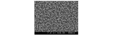
- substrate SEM image of boehmite layer surface
- Enlarged view of part IVB at the bottom of the side surface of the photoelectric field enhancement substrate 2 shown in FIG. 4A Diagram showing the wavelength dependence of the light reflectivity of the boehmite layer Plan view showing a photoelectric field enhancement sample cell 3 according to a third embodiment of the photoelectric field enhancement device.
- FIG. 6A Schematic diagram showing the configuration of an enhanced Raman spectroscopic device provided with a photoelectric field enhancing substrate 1 Schematic showing an example of design change of an enhanced Raman spectrometer Schematic diagram showing the configuration of an enhanced Raman spectrometer equipped with a photoelectric field enhancing sample cell 3 Graph showing the Raman spectrum distribution obtained for the measurement sample Graph showing the dependence of Raman signal intensity obtained on measurement sample on Au vapor deposition film thickness
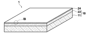
- FIG. 1A is a perspective view showing a photoelectric field enhancement substrate 1 according to the first embodiment of the photoelectric field enhancement device of the present invention
- FIG. 1B is a part of a side surface of the photoelectric field enhancement substrate 1 shown in FIG. 1A. It is an enlarged view of IB.
- the photoelectric field enhancing substrate 1 includes a transparent substrate 10 having a fine uneven structure 23 on the surface, and a metal fine uneven structure layer 24 formed on the surface of the fine uneven structure 23.
- excitation light irradiated to the fine concavo-convex structure 25 of the metal fine concavo-convex structure layer 24, and the metal fine concavo-convex structure layer 24 is induced by this local plasmon resonance. This produces an enhanced photoelectric field on the surface of the film.
- the metal fine concavo-convex structure layer 24 has a fine concavo-convex structure in which the interval between adjacent convex portions is smaller than the interval between adjacent convex portions of the fine concavo-convex structure 23 of the transparent substrate 10 that corresponds between the adjacent convex portions.
- the interval Wm between the convex portion 25a and the convex portion 25b adjacent thereto corresponds to the convex portions 25a and 25b. It suffices if there is a portion that is smaller than the interval Wb between the convex portion 23a and the convex portion 23b of the fine concavo-convex structure 23 of the transparent substrate.
- the interval Wm is half the depth Dm from the apex of the lower convex portion 25b of the adjacent convex portions 25a and 25b to the deepest portion 25c of the concave portion between both convex portions 25a and 25b.
- the interval Wb is half the depth Db from the apex of the lower convex portion 23b of the adjacent convex portions 23a and 23b to the deepest portion 23c of the concave portion between both convex portions 23a and 23b. This is the distance between the convex portions 23a and 23b at the position of the depth Db / 2.
- the convex portions 24a are rounded and the distance between adjacent convex portions is smaller than when the metal is simply formed in a film shape along the fine concavo-convex structure 23 of the transparent substrate 10.
- the fine concavo-convex structure 25 of the metal fine concavo-convex structure layer 24 is such that at least one of the length in the direction perpendicular to the substrate and the length in the direction horizontal to the substrate is shorter than the wavelength of the excitation light. Any fine concavo-convex structure may be used as long as it can generate localized plasmons on the surface of the metal fine concavo-convex structure layer 24.
- the convex portions of the metal fine concavo-convex structure layer 24 are preferably in the form of particles formed by aggregation of metals. It is desirable that the granular convex portions have an aspect ratio (length in the direction perpendicular to the substrate / length in the horizontal direction on the substrate) of 0.5 or more.
- the average depth from the top of the convex portion of the fine concave-convex structure 25 of the metal fine concave-convex structure layer 24 to the bottom of the adjacent concave portion is 200 nm or less, and the average pitch between the vertices of the nearest convex portions separating the concave portions is 200 nm or less. Preferably there is.
- the average thickness of the metal fine concavo-convex structure layer 24 generates an efficiently enhanced photoelectric field on the surface opposite to the transparent substrate of the metal fine concavo-convex structure layer with respect to light irradiated from the transparent substrate side. Thickness is preferred.
- the thickness is preferably 400 nm or less for gold and 90 nm or less for silver. The thickness at this time is not a measured value of the thickness, but means that the thickness is deposited on the flat plate substrate by the deposition amount required for depositing a metal such as gold or silver.
- the distance between all adjacent convex portions of the fine concavo-convex structure in the metal fine concavo-convex structure layer is smaller than the interval between adjacent convex portions of the corresponding fine concavo-convex structure of the substrate.
- the effect of enhancing the photoelectric field becomes more prominent as the number of adjacent convex portions of the metal fine concavo-convex structure layer that is smaller than the interval between adjacent convex portions of the corresponding fine concavo-convex structure of the substrate increases.
- a very strong photoelectric field enhancement field called a hot spot is generated in the gap between the convex portions by light irradiation. For this reason, it is preferable that there are many places where the distance between adjacent convex portions is 20 nm or less. In addition, adjacent convex parts may be contacting partially.
- the metal fine concavo-convex structure layer 24 is particularly preferably a granular convex part formed so that the convex part extends in a granular manner from the surface of the fine concavo-convex structure 23 of the transparent substrate 10. If it is granular, the surface area increases, so the number of analytes attached to the metal surface can be increased, leading to an increase in detection light.
- the metal constituting the metal fine concavo-convex structure layer 24 may be any metal that can generate localized plasmon when irradiated with excitation light.
- Au or Ag is preferable.
- the transparent substrate 10 includes a transparent substrate body 11 made of glass or the like, and a transparent fine substrate made of a material different from the transparent substrate body 11 constituting the fine uneven structure 23 provided on the surface of the transparent substrate 10.
- the concavo-convex structure layer 22 is used.
- the transparent fine concavo-convex structure layer 22 is preferably a boehmite layer, but the transparent fine concavo-convex structure layer 22 may be made of Bayerlite in addition to boehmite. Moreover, you may be comprised from the hydroxide of another metal or the hydroxide of a metal oxide.
- the fine concavo-convex structure 23 is not limited to the one made of a material different from that of the transparent substrate body, but may be made of the same material as the substrate body by processing the surface of the transparent substrate body.
- a glass substrate having a surface with a fine concavo-convex structure formed by dry etching treatment with any of lithography, ion beam lithography, and nanoimprint may be used as the transparent substrate.
- the fine concavo-convex structure 23 is constituted by the boehmite layer 22.
- the transparent fine concavo-convex structure 23 made of a metal such as a boehmite layer or a hydroxide of a metal oxide has various sizes (vertical angle sizes) and orientations, but has a generally serrated cross section. have.
- the transparent fine concavo-convex structure 23 may be any structure as long as the metal fine concavo-convex structure layer 24 can be formed on the transparent fine concavo-convex structure 23.
- the pitch is the distance between the vertices of the nearest adjacent convex portions across the concave portion
- the depth is the distance from the convex vertex to the bottom of the adjacent concave portion.
- a plate-like transparent substrate body 11 is prepared, and the transparent substrate body 11 is washed with acetone and methanol. Thereafter, the aluminum 20 is deposited on the surface of the substrate body 11 by a sputtering method to a thickness of about several tens of nanometers. Thereafter, the transparent substrate body 11 with aluminum 20 is immersed in boiling pure water, and is taken out after several minutes (about 5 minutes). By this boiling treatment (boehmite treatment), the aluminum 20 becomes transparent and becomes a boehmite layer 22 constituting a fine concavo-convex structure. Next, by depositing a metal on the boehmite layer 22, a metal fine concavo-convex structure layer 24 is generated on the boehmite layer 22.
- the photoelectric field enhancing substrate 1 can be manufactured by the above processing.
- FIG. 3A shows a boehmite of a transparent substrate comprising a boehmite layer formed by sputtering a 25 nm aluminum film on a transparent substrate body (BK-7; Corning Eagle 2000) and then boiling it for 5 minutes.
- FIG. 3B to FIG. 3D are SEM images obtained by photographing the surface of the substrate and the substrate surface on which Au was deposited on the boehmite layer by 30 nm, 60 nm, and 150 nm, respectively, with SEM (Hitachi S4100).
- Al is vapor-deposited for 30 nm, 60 nm, and 150 nm” means that it is vapor-deposited with a vapor deposition amount of 30 nm, 60 nm, and 150 nm when vapor-deposited on a flat substrate.
- FIGS. 3A to 3D white portions are observed as convex portions, and gray portions are observed as concave portions.
- the uneven pattern is irregular, it is uniformly formed on the entire surface, and the in-plane uniformity of the fine uneven structure is high.
- the concavo-convex structure is composed of a number of ridge-shaped convex portions.
- the uneven structure cross section of the boehmite layer has a sawtooth shape as schematically shown in FIG. 1B. As shown in FIG.
- the convex portions of the concavo-convex structure formed in the boehmite layer are thick and the convex portion interval is narrow.
- the concave fine concavo-convex structure of the metal fine concavo-convex structure layer shown in FIG. 3B is a concavo-convex structure having a convex portion in which the ridge-like convex structure seen on the surface of the boehmite layer is substantially maintained.
- the convex portions are observed in a granular form, and the interval between the convex portions becomes closer. It is observed as an uneven structure different from the uneven structure on the boehmite layer surface.
- FIG. 3E is an SEM image of a cross section of a metal fine concavo-convex structure layer obtained by depositing 150 nm of Au on the boehmite layer. From the image of this cross section, the convex portion extends upward from the boehmite side and has a larger aspect ratio, and the metal fine concavo-convex structure is a granular fine structure in which a large number of granular convex portions are formed. I understand that. In addition, a large number of regions in which the intervals between the granular convex portions are very close are formed.
- FIG. 4A is a perspective view showing the photoelectric field enhancement substrate 2 of the present embodiment
- FIG. 4B is an enlarged view of a part IVB at the lower side of the photoelectric field enhancement substrate 2 shown in FIG. 4A.
- the photoelectric field enhancement substrate 2 of the present embodiment includes a second transparent fine concavo-convex structure layer 28 on the back side of the photoelectric field enhancement substrate 1 of the first embodiment.
- the second transparent fine concavo-convex structure layer 28 is the same as the first fine concavo-convex structure layer 22 provided on the surface side of the transparent substrate 10, and can be composed of a boehmite layer.
- the fine uneven structure layer 28 on the back side functions as an antireflection film when irradiated with light.
- the photoelectric field enhancement substrate 2 of the present embodiment is formed by depositing aluminum not only on the front surface but also on the back surface of the transparent substrate body 11 in the method for producing the photoelectric field enhancement substrate 1 of the first embodiment, and then boiled. Can be obtained. By boiling in pure water, the front and back aluminum becomes boehmite, and the same transparent fine uneven structure layers 22 and 28 can be provided on the front and back surfaces.
- FIG. 5 shows a boehmite layer formed on a substrate having a boehmite layer formed by sputtering for 5 minutes after sputtering 50 nm aluminum on a transparent substrate (BK-7; Corning Eagle 2000). It shows the reflectance when light is incident from the surface side from the direction perpendicular to the surface. In the case of this example, a reflectance of about 0.1% is achieved for a wavelength near 650 nm. The wavelength with the lowest reflectivity can be adjusted by controlling the interference by changing the thickness of the aluminum that is first sputtered.
- FIG. 6A is a plan view showing the photoelectric field enhancing sample cell 3 of the third embodiment
- FIG. 6B is a sectional view taken along the line VIB-VIB of the photoelectric field enhancing sample cell 3 shown in FIG. 6A.
- the photoelectric field enhancing sample cell 3 of this embodiment includes a transparent substrate main body 31, a transparent fine uneven structure layer 32 provided on the surface thereof, and a metal fine uneven structure layer 34 provided on the fine uneven structure layer 32. And a liquid sample holding member 35 for holding a liquid sample on the metal fine concavo-convex structure layer 34.
- the photoelectric field enhancement substrate 30 has substantially the same configuration as the photoelectric field enhancement substrate 1 of the first embodiment. That is, the transparent fine uneven structure layer 32 and the metal fine uneven structure layer 34 are the same as the transparent fine uneven structure layer 22 and the metal fine uneven structure layer 24 of the first photoelectric field enhancement device 1 shown in FIG. 1B. The constituent materials and the forming method are also the same.
- the liquid sample holding member 35 holds, for example, a liquid sample on the metal fine concavo-convex structure layer 34 and forms a liquid sample flow path 36a, an inlet (inlet) 38a for injecting the sample, and a flow
- a transparent upper plate 38 such as a glass plate provided with a discharge port (outlet) 38b for discharging the liquid sample flowing down the path 36a can be used.
- the photoelectric field enhancing sample cell 3 of the present embodiment can be obtained by fabricating the photoelectric field enhancing substrate 30 by the same method as that of the substrate 1 of the first embodiment and then bonding the spacer portion 36 and the upper plate 38. it can.
- the spacer portion 36 and the upper plate 38 may be integrally formed.
- the spacer part 36 may be formed integrally with the transparent substrate body 31.
- the flow channel sample cell (flow cell) type photoelectric field enhancement device provided with an inlet and an outlet has been described. It is good also as a photoelectric field enhancement sample cell which hold
- a second transparent functioning as an antireflection film is provided on the back surface of the region where the metal fine concavo-convex structure layer 34 of the photoelectric field enhancement substrate 30 is provided, like the photoelectric field enhancement substrate 2 of the second embodiment. You may make it provide a fine fine uneven
- the photoelectric field enhancement device of the present invention described in each of the above embodiments has a subject placed on the metal fine concavo-convex structure layer of the device, irradiated with excitation light to the place where the subject is placed, and the excitation light. It can be suitably used for a measurement method and apparatus for detecting light generated from a subject by irradiation of. For example, it can be applied to enhanced Raman spectroscopy, fluorescence detection method, etc., can be used as a Raman enhancement device in enhanced Raman spectroscopy, and can be used as a fluorescence enhancement device in fluorescence detection method.
- the photoelectric field enhancement device of the present invention is used not only for detection of Raman scattered light and fluorescence, but also for detection of Rayleigh scattered light, Mie scattered light, second harmonics, and the like generated from an object irradiated with excitation light.
- enhanced light can be detected by the enhanced photoelectric field associated with localized plasmon resonance.
- FIG. 7 is a schematic diagram showing a configuration of an enhanced Raman spectroscopic device including the photoelectric field enhancing substrate 1 according to the first embodiment described above.
- the Raman spectroscopic device 100 includes the above-described photoelectric field enhancement substrate 1, the excitation light irradiation unit 140 that irradiates the photoelectric field enhancement substrate 1 with the excitation light L1, and the photoelectric field enhancement emitted from the subject S. And a light detection unit 150 for detecting Raman scattered light L2 enhanced by the action of the substrate.
- the excitation light irradiation unit 140 includes a semiconductor laser 141 that emits the excitation light L1, a mirror 142 that reflects the light L1 emitted from the semiconductor laser 141 toward the substrate 1, and the excitation light L1 reflected by the mirror 142. Transmitted through the half mirror 144 and the half mirror 144 that reflects light from the substrate 1 side including the enhanced Raman scattered light L2 generated from the subject S by irradiation of the excitation light L1 to the light detection unit 150 side And a lens 146 that condenses the excitation light L1 in a region of the photoelectric field enhancement substrate 1 on which the subject S is placed.
- the light detection unit 150 absorbs the excitation light L1 out of the light reflected by the half mirror 144 and transmits the other light, and a pin provided with a pinhole 152 for removing noise light.
- a lens 154 for condensing the enhanced Raman scattered light L2 emitted from the Hall plate 153, the subject S, and transmitted through the lens 146 and the notch filter 151 to the pinhole 152, and the Raman scattered light passing through the pinhole 152 Is provided with a lens 156 for collimating light and a spectroscope 158 for detecting enhanced Raman scattered light.
- Excitation light L1 is emitted from the semiconductor laser 141 of the light irradiation unit 140, the excitation light L1 is reflected to the substrate 1 side by the mirror 142, passes through the half mirror 144 and is collected by the lens 146, and the photoelectric field enhancement substrate 1 Irradiated on top.
- the irradiation of the excitation light L1 induces localized plasmon resonance in the metal fine concavo-convex structure layer 24 of the photoelectric field enhancing substrate 1, and an enhanced photoelectric field is generated on the surface of the metal fine concavo-convex structure layer 24.
- the Raman scattered light L2 emitted from the subject S enhanced by the enhanced photoelectric field passes through the lens 146 and is reflected by the half mirror 144 toward the spectroscope 158 side. At this time, the excitation light L1 reflected by the photoelectric field enhancement substrate 1 is also reflected by the half mirror 144 and reflected to the spectroscope 158 side, but the excitation light L1 is cut by the notch filter 151.
- the wavelength of Rayleigh scattered light (or Mie scattered light) is the same as that of the excitation light L 1, so that it is cut by the notch filter 151 and does not enter the spectroscope 158.
- the Raman scattered light L2 enters the spectroscope 158 and is subjected to Raman spectrum measurement.
- the Raman spectroscopic device 100 of the present embodiment is configured using the photoelectric field enhancement substrate 1 of the above embodiment, and since the Raman enhancement is effectively performed, the data reliability is high and the data reproducibility is high. Good high-precision Raman spectroscopic measurement can be performed. Since the in-plane uniformity of the surface concavo-convex structure of the photoelectric field enhancing substrate 1 is high, data with good reproducibility can be obtained even if the same sample is measured by changing the light irradiation location. Therefore, it is possible to obtain a plurality of data by changing the light irradiation location for the same sample, thereby improving the reliability of the data.
- the metal fine concavo-convex structure layer and the subject can be detected from the back side of the transparent substrate without being shielded by the subject itself.
- the present inventors confirmed that the enhanced Raman scattering light can be detected from the back side of the transparent substrate without being affected by the metal fine uneven structure layer if the metal fine uneven structure layer has a certain thickness. (See Examples below).
- the Raman spectroscopic apparatus 100 is configured so that excitation light is incident from the side opposite to the sample holding surface (front surface) of the photoelectric field enhancing device 1 (back surface of the device) and Raman scattered light is detected.
- the excitation light L1 is incident from the surface side (sample holding surface) of the metal fine concavo-convex structure layer 24 and the Raman scattering is performed as in the conventional device. You may comprise so that the light L2 may be detected.
- either the excitation light irradiation part or the light detection part may be arranged on the surface side of the metal fine concavo-convex structure layer 24 and the other may be arranged on the back side of the substrate 1.
- the photoelectric field enhancement device of the present invention uses a transparent substrate, light can be irradiated from either the surface side of the metal fine concavo-convex structure layer or the back side of the transparent substrate, Light generated from the sample by this light irradiation can also be detected from either the surface side of the metal fine concavo-convex structure layer or the back side of the transparent substrate. Therefore, depending on the type, size, etc. of the subject, irradiation of excitation light and detection of detection light can be performed from either the front surface side of the metal fine concavo-convex structure layer or the back surface side of the transparent substrate. The degree is high, and it becomes possible to detect at a higher S / N.
- FIG. 9 is a schematic diagram illustrating a schematic configuration of a Raman spectroscopic device 120 including a flow cell that is the photoelectric field enhancement device 3 of the above-described third embodiment.
- the Raman spectroscopic device 120 shown in FIG. 9 differs from the Raman spectroscopic device 100 shown in FIG. 7 in that a flow cell type photoelectric field enhancing sample cell 3 is provided instead of the photoelectric field enhancing substrate 1.
- a flow cell type photoelectric field enhancement device Raman spectroscopy can be measured while flowing a liquid sample as an object.
- the measurement of the flow cell type device 3 may be configured such that excitation light is incident from the surface side of the metal fine concavo-convex structure layer and Raman scattered light is detected from the surface side of the metal fine concavo-convex structure layer.
- the transmittance and the absorptance of the liquid sample with respect to the Raman scattered light may vary with the movement of the liquid sample. As shown in FIG. 4, it is preferable that the Raman scattered light is detected from the back side of the substrate 30.
- the photoelectric field enhancement device of the present invention can be applied to a plasmon enhanced fluorescence detection apparatus.
- the subject may be placed on the metal fine concavo-convex structure layer of the photoelectric field enhancing device, and excitation light may be irradiated from the subject side to detect the enhanced fluorescence from the subject side.
- the excitation light may be irradiated from the back side of the transparent substrate, and the fluorescence may be detected from the back side.
- you may irradiate excitation light from the subject side and you may comprise so that fluorescence may be detected from the transparent substrate back surface side.
- Method for producing photoelectric field enhancement substrate As the transparent substrate body 11, a glass substrate (BK-7; Eagle 2000 manufactured by Corning) was used. After ultrasonic cleaning (45 kHz) for 5 minutes with acetone and 5 minutes with methanol, 25 nm of aluminum 20 was laminated on the glass substrate 11 using a sputtering apparatus (manufactured by Canon Anelva). In addition, the aluminum thickness was measured using the surface shape measuring device (made by TENCOR), and it confirmed that thickness was 25 nm (+/- 10%).
- Raman scattered light was detected using a microscopic Raman spectroscope (HR800).
- HR800 Raman spectroscope
- laser light having a peak wavelength of 785 nm was used and observed at a magnification of 20 times.
- FIG. 10 is a graph showing a Raman shift spectrum distribution obtained by detecting Raman scattered light from the front and back of a substrate using a sample (Example 2) in which Au is deposited by 60 nm.
- the measurement from the surface of the substrate is a method in which excitation light is irradiated from the dye surface side on the metal fine concavo-convex structure layer, and Raman scattered light is detected from the dye surface side on the metal fine concavo-convex structure layer.
- the measurement from the back side is the one that irradiates excitation light from the transparent fine concavo-convex structure side under the metal fine concavo-convex structure layer (irradiates excitation light from the back side of the substrate) and detects Raman scattered light from the back side of the substrate. is there.
- FIG. 10 shows that the Raman shift signal can be detected with the same intensity at almost the same location on the front and back of the substrate.
- Raman measurement there was no example of detecting a Raman signal from the back side of the substrate, but according to the Raman measurement using the photoelectric field enhancement device of the present invention, the Raman signal was detected from the back side of the substrate. It is clear that it can be detected.
- the dye used as a specimen in the measurement sample was dried and fixed, and the thickness of the specimen was very thin. Therefore, the signal intensity from the front and back surfaces was the same level.
- Raman spectroscopy when performing Raman spectroscopy on a sample having a thickness of the order of 1 ⁇ m such as a cell, it is better to detect the signal near the interface between the metal fine concavo-convex structure layer and the sample with a high enhancement effect from the back side. It is considered advantageous.
- FIG. 11 shows the peak intensity of 1360 cm ⁇ 1 after the removal of white noise and the Au deposited film thickness using the Raman shift spectrum distribution obtained by detecting the Raman scattered light from the surface of the substrate for each sample of Examples 1 to 3. Is a graph plotted with the horizontal axis.
- the deposition film thickness of Au increases, the Au becomes granular as shown in the SEM images of FIGS. 3B to 3D, and further, the surface area of the metal fine concavo-convex structure increases and the metal protrusions. It is considered that the signal strength increases because a large number of hot spots are generated due to a decrease in the distance between them.
Landscapes
- Chemical & Material Sciences (AREA)
- Physics & Mathematics (AREA)
- Health & Medical Sciences (AREA)
- Life Sciences & Earth Sciences (AREA)
- Engineering & Computer Science (AREA)
- Analytical Chemistry (AREA)
- Pathology (AREA)
- Immunology (AREA)
- General Physics & Mathematics (AREA)
- General Health & Medical Sciences (AREA)
- Biochemistry (AREA)
- Nanotechnology (AREA)
- Nuclear Medicine, Radiotherapy & Molecular Imaging (AREA)
- Optics & Photonics (AREA)
- Electromagnetism (AREA)
- Biophysics (AREA)
- Crystallography & Structural Chemistry (AREA)
- Plasma & Fusion (AREA)
- Investigating, Analyzing Materials By Fluorescence Or Luminescence (AREA)
- Investigating Or Analysing Materials By Optical Means (AREA)
Abstract
L'invention vise à proposer un dispositif de renforcement de champ électrique optique pouvant détecter une lumière à diffusion de Raman avec une sensibilité accrue. À cet effet, le dispositif selon l'invention est pourvu d'un substrat transparent (10) présentant à sa surface une structure à microreliefs (23) et une couche à structure à microreliefs métallique (24) formée sur la surface de la structure à microreliefs (23); la couche à structure à microreliefs métallique (24) présente une structure à microreliefs (25) dans laquelle l'espace (Wm) entre des sections convexes adjacentes est inférieur à l'espace (Wb) entre les sections convexes adjacentes correspondantes de la structure à microreliefs (23) du substrat transparent (10).
Priority Applications (3)
| Application Number | Priority Date | Filing Date | Title |
|---|---|---|---|
| CN201280014387.5A CN103430012B (zh) | 2011-03-22 | 2012-03-16 | 光电场增强装置和配备有该装置的测量设备 |
| EP12760569.9A EP2690427B1 (fr) | 2011-03-22 | 2012-03-16 | Dispositif de renforcement de champ électrique optique et dispositif de mesure pourvu d'un tel dispositif |
| US14/033,127 US9059568B2 (en) | 2011-03-22 | 2013-09-20 | Optical electrical field enhancing device and measuring apparatus equipped with the device |
Applications Claiming Priority (2)
| Application Number | Priority Date | Filing Date | Title |
|---|---|---|---|
| JP2011-062091 | 2011-03-22 | ||
| JP2011062091A JP5848013B2 (ja) | 2011-03-22 | 2011-03-22 | 光電場増強デバイスおよび該デバイスを備えた測定装置 |
Related Child Applications (1)
| Application Number | Title | Priority Date | Filing Date |
|---|---|---|---|
| US14/033,127 Continuation US9059568B2 (en) | 2011-03-22 | 2013-09-20 | Optical electrical field enhancing device and measuring apparatus equipped with the device |
Publications (1)
| Publication Number | Publication Date |
|---|---|
| WO2012127841A1 true WO2012127841A1 (fr) | 2012-09-27 |
Family
ID=46879021
Family Applications (1)
| Application Number | Title | Priority Date | Filing Date |
|---|---|---|---|
| PCT/JP2012/001866 Ceased WO2012127841A1 (fr) | 2011-03-22 | 2012-03-16 | Dispositif de renforcement de champ électrique optique et dispositif de mesure pourvu d'un tel dispositif |
Country Status (5)
| Country | Link |
|---|---|
| US (1) | US9059568B2 (fr) |
| EP (1) | EP2690427B1 (fr) |
| JP (1) | JP5848013B2 (fr) |
| CN (1) | CN103430012B (fr) |
| WO (1) | WO2012127841A1 (fr) |
Cited By (2)
| Publication number | Priority date | Publication date | Assignee | Title |
|---|---|---|---|---|
| WO2014156088A1 (fr) * | 2013-03-27 | 2014-10-02 | 富士フイルム株式会社 | Dispositif d'amélioration de champ photoélectrique et procédé de fabrication associé |
| JPWO2016031140A1 (ja) * | 2014-08-27 | 2017-05-25 | 富士フイルム株式会社 | 光電場増強デバイス |
Families Citing this family (12)
| Publication number | Priority date | Publication date | Assignee | Title |
|---|---|---|---|---|
| JP2719125B2 (ja) | 1995-09-14 | 1998-02-25 | 中外炉工業株式会社 | 鋼管の管内パージ方法 |
| JP2012242167A (ja) * | 2011-05-17 | 2012-12-10 | Fujifilm Corp | ラマン分光測定方法および装置 |
| US9719931B2 (en) * | 2013-07-18 | 2017-08-01 | Optokey, Inc. | Surface enhanced raman spectroscopy resonator structures and methods of making same |
| US20150049332A1 (en) * | 2013-07-30 | 2015-02-19 | The Curators Of The University Of Missouri | Gold nanoisland arrays |
| JP6634217B2 (ja) * | 2014-04-08 | 2020-01-22 | 地方独立行政法人東京都立産業技術研究センター | 局在表面プラズモン共鳴センサ、ガスセンサ及び製造方法 |
| WO2016051666A1 (fr) * | 2014-09-30 | 2016-04-07 | 富士フイルム株式会社 | Dispositif de renforcement de champ optique électrique pour détecter le dioxyde de carbone gazeux |
| US10072984B2 (en) * | 2014-10-02 | 2018-09-11 | Mks Technology, Inc. | Spectrometer |
| JP6780607B2 (ja) * | 2017-08-10 | 2020-11-04 | 王子ホールディングス株式会社 | 分析用基板およびその製造方法 |
| JP7398639B2 (ja) * | 2018-08-24 | 2023-12-15 | パナソニックIpマネジメント株式会社 | 金属微細構造体および検出装置 |
| JP7442781B2 (ja) * | 2019-10-29 | 2024-03-05 | 国立研究開発法人産業技術総合研究所 | プラズモニックセンサ用の部材およびその製造方法 |
| KR102819088B1 (ko) * | 2021-12-22 | 2025-06-12 | 한국재료연구원 | 신속 고감도 병원체 검출 장치 및 이를 이용한 병원체 분석 방법 |
| CN116359203B (zh) * | 2023-05-09 | 2026-02-06 | 深圳市笨辉光电科技有限公司 | 一种表面场增强辅助容器 |
Citations (12)
| Publication number | Priority date | Publication date | Assignee | Title |
|---|---|---|---|---|
| JPS6148124B2 (fr) * | 1977-02-18 | 1986-10-22 | Minnesota Mining & Mfg | |
| JP2004279364A (ja) * | 2003-03-19 | 2004-10-07 | Fuji Photo Film Co Ltd | センサチップおよびセンサチップの製造方法並びにそのセンサチップを用いたセンサ |
| JP2005172569A (ja) | 2003-12-10 | 2005-06-30 | Fuji Photo Film Co Ltd | 微細構造体、微細構造体の作製方法、ラマン分光方法および装置 |
| WO2005078415A1 (fr) * | 2004-02-13 | 2005-08-25 | Omron Corporation | Capteur de résonance plasmon de surface |
| JP2006514286A (ja) | 2003-02-18 | 2006-04-27 | インテル・コーポレーション | 活性表面増強ラマン分光分析(sers)の基体としての金属被覆ナノ結晶シリコン |
| JP2006145230A (ja) | 2004-11-16 | 2006-06-08 | Canon Inc | 被分析物担体およびその製造方法 |
| JP2008216055A (ja) * | 2007-03-05 | 2008-09-18 | Omron Corp | 表面プラズモン共鳴センサ及び当該センサ用チップ |
| JP2009236830A (ja) * | 2008-03-28 | 2009-10-15 | Sumitomo Precision Prod Co Ltd | 被分析物担体、及び、その製造方法 |
| JP4347801B2 (ja) | 2002-06-12 | 2009-10-21 | インテル・コーポレーション | 活性表面増強ラマン分光(sers)基板としての金属被覆ナノ結晶性シリコン |
| JP2010203900A (ja) * | 2009-03-03 | 2010-09-16 | Konica Minolta Holdings Inc | 表面プラズモン増強蛍光センサおよび表面プラズモン増強蛍光センサに用いられるチップ構造体 |
| JP2012063294A (ja) * | 2010-09-17 | 2012-03-29 | Fujifilm Corp | 光電場増強デバイスを用いた光の測定方法および測定装置 |
| JP2012063293A (ja) * | 2010-09-17 | 2012-03-29 | Fujifilm Corp | 光電場増強デバイス |
Family Cites Families (7)
| Publication number | Priority date | Publication date | Assignee | Title |
|---|---|---|---|---|
| JPS6148124A (ja) | 1984-08-14 | 1986-03-08 | Fuji Photo Film Co Ltd | 磁気記録媒体 |
| JPH09202649A (ja) * | 1996-01-24 | 1997-08-05 | Central Glass Co Ltd | 花弁状透明アルミナ膜及びその形成法 |
| AU2009401A (en) * | 1999-12-17 | 2001-06-25 | Zeptosens Ag | Flow cell array and the utilization thereof for multianalyte determination |
| EP1445601A3 (fr) * | 2003-01-30 | 2004-09-22 | Fuji Photo Film Co., Ltd. | Puces pour la mesure par résonnance de plasmons de surface locale, procédés de fabrication de ces puces, et des capteurs employant ces puces |
| US7911693B2 (en) * | 2006-03-20 | 2011-03-22 | Hewlett-Packard Development Company, L.P. | Ambient light absorbing screen |
| JP4762801B2 (ja) * | 2006-06-27 | 2011-08-31 | 富士フイルム株式会社 | センサ、センシング装置 |
| JP2009109395A (ja) * | 2007-10-31 | 2009-05-21 | Fujifilm Corp | 微細構造体の作製方法、微細構造体、ラマン分光用デバイス、ラマン分光装置、分析装置、検出装置、および質量分析装置 |
-
2011
- 2011-03-22 JP JP2011062091A patent/JP5848013B2/ja not_active Expired - Fee Related
-
2012
- 2012-03-16 EP EP12760569.9A patent/EP2690427B1/fr not_active Not-in-force
- 2012-03-16 WO PCT/JP2012/001866 patent/WO2012127841A1/fr not_active Ceased
- 2012-03-16 CN CN201280014387.5A patent/CN103430012B/zh not_active Expired - Fee Related
-
2013
- 2013-09-20 US US14/033,127 patent/US9059568B2/en not_active Expired - Fee Related
Patent Citations (12)
| Publication number | Priority date | Publication date | Assignee | Title |
|---|---|---|---|---|
| JPS6148124B2 (fr) * | 1977-02-18 | 1986-10-22 | Minnesota Mining & Mfg | |
| JP4347801B2 (ja) | 2002-06-12 | 2009-10-21 | インテル・コーポレーション | 活性表面増強ラマン分光(sers)基板としての金属被覆ナノ結晶性シリコン |
| JP2006514286A (ja) | 2003-02-18 | 2006-04-27 | インテル・コーポレーション | 活性表面増強ラマン分光分析(sers)の基体としての金属被覆ナノ結晶シリコン |
| JP2004279364A (ja) * | 2003-03-19 | 2004-10-07 | Fuji Photo Film Co Ltd | センサチップおよびセンサチップの製造方法並びにそのセンサチップを用いたセンサ |
| JP2005172569A (ja) | 2003-12-10 | 2005-06-30 | Fuji Photo Film Co Ltd | 微細構造体、微細構造体の作製方法、ラマン分光方法および装置 |
| WO2005078415A1 (fr) * | 2004-02-13 | 2005-08-25 | Omron Corporation | Capteur de résonance plasmon de surface |
| JP2006145230A (ja) | 2004-11-16 | 2006-06-08 | Canon Inc | 被分析物担体およびその製造方法 |
| JP2008216055A (ja) * | 2007-03-05 | 2008-09-18 | Omron Corp | 表面プラズモン共鳴センサ及び当該センサ用チップ |
| JP2009236830A (ja) * | 2008-03-28 | 2009-10-15 | Sumitomo Precision Prod Co Ltd | 被分析物担体、及び、その製造方法 |
| JP2010203900A (ja) * | 2009-03-03 | 2010-09-16 | Konica Minolta Holdings Inc | 表面プラズモン増強蛍光センサおよび表面プラズモン増強蛍光センサに用いられるチップ構造体 |
| JP2012063294A (ja) * | 2010-09-17 | 2012-03-29 | Fujifilm Corp | 光電場増強デバイスを用いた光の測定方法および測定装置 |
| JP2012063293A (ja) * | 2010-09-17 | 2012-03-29 | Fujifilm Corp | 光電場増強デバイス |
Non-Patent Citations (2)
| Title |
|---|
| OPTICS EXPRESS, vol. 17, no. 21, pages 18556 |
| See also references of EP2690427A4 |
Cited By (4)
| Publication number | Priority date | Publication date | Assignee | Title |
|---|---|---|---|---|
| WO2014156088A1 (fr) * | 2013-03-27 | 2014-10-02 | 富士フイルム株式会社 | Dispositif d'amélioration de champ photoélectrique et procédé de fabrication associé |
| JP2014190834A (ja) * | 2013-03-27 | 2014-10-06 | Fujifilm Corp | 光電場増強デバイスおよびその製造方法 |
| US10094956B2 (en) | 2013-03-27 | 2018-10-09 | Fujifilm Corporation | Optical field enhancement device and manufacturing method of the same |
| JPWO2016031140A1 (ja) * | 2014-08-27 | 2017-05-25 | 富士フイルム株式会社 | 光電場増強デバイス |
Also Published As
| Publication number | Publication date |
|---|---|
| EP2690427B1 (fr) | 2017-03-01 |
| JP5848013B2 (ja) | 2016-01-27 |
| CN103430012A (zh) | 2013-12-04 |
| CN103430012B (zh) | 2016-06-22 |
| US9059568B2 (en) | 2015-06-16 |
| US20140016127A1 (en) | 2014-01-16 |
| EP2690427A4 (fr) | 2014-09-03 |
| JP2012198090A (ja) | 2012-10-18 |
| EP2690427A1 (fr) | 2014-01-29 |
Similar Documents
| Publication | Publication Date | Title |
|---|---|---|
| JP5848013B2 (ja) | 光電場増強デバイスおよび該デバイスを備えた測定装置 | |
| JP5552007B2 (ja) | 光電場増強デバイス | |
| JP5553717B2 (ja) | 光電場増強デバイスを用いた光の測定方法および測定装置 | |
| JP5801587B2 (ja) | 光電場増強デバイスの製造方法 | |
| JP2008002943A (ja) | センサ、センシング装置、及びセンシング方法 | |
| WO2015146036A1 (fr) | Dispositif de spectroscopie raman amélioré | |
| JP6337127B2 (ja) | 光電場増強デバイスおよび光電場増強デバイスの製造方法 | |
| WO2014156088A1 (fr) | Dispositif d'amélioration de champ photoélectrique et procédé de fabrication associé | |
| JP2014016221A (ja) | 光電場増強デバイスおよびその製造方法 | |
| JP5947182B2 (ja) | 光電場増強デバイスを用いた測定装置 | |
| JP5988239B2 (ja) | 蛍光測定用基板 | |
| Jing | REALIZATION OF PLASMONIC 2D & 3D NANOSTRUCTURES FOR SURFACE ENHANCED RAMAN SCATTERING DETECTION. | |
| JPWO2016051666A1 (ja) | 炭酸ガスセンシング用の光電場増強デバイス |
Legal Events
| Date | Code | Title | Description |
|---|---|---|---|
| 121 | Ep: the epo has been informed by wipo that ep was designated in this application |
Ref document number: 12760569 Country of ref document: EP Kind code of ref document: A1 |
|
| NENP | Non-entry into the national phase |
Ref country code: DE |
|
| REEP | Request for entry into the european phase |
Ref document number: 2012760569 Country of ref document: EP |
|
| WWE | Wipo information: entry into national phase |
Ref document number: 2012760569 Country of ref document: EP |