WO2012132232A1 - Dispositif luminescent à semi-conducteurs - Google Patents
Dispositif luminescent à semi-conducteurs Download PDFInfo
- Publication number
- WO2012132232A1 WO2012132232A1 PCT/JP2012/001398 JP2012001398W WO2012132232A1 WO 2012132232 A1 WO2012132232 A1 WO 2012132232A1 JP 2012001398 W JP2012001398 W JP 2012001398W WO 2012132232 A1 WO2012132232 A1 WO 2012132232A1
- Authority
- WO
- WIPO (PCT)
- Prior art keywords
- semiconductor light
- resin layer
- fine particles
- light emitting
- emitting device
- Prior art date
- Legal status (The legal status is an assumption and is not a legal conclusion. Google has not performed a legal analysis and makes no representation as to the accuracy of the status listed.)
- Ceased
Links
Images




Classifications
-
- H—ELECTRICITY
- H10—SEMICONDUCTOR DEVICES; ELECTRIC SOLID-STATE DEVICES NOT OTHERWISE PROVIDED FOR
- H10H—INORGANIC LIGHT-EMITTING SEMICONDUCTOR DEVICES HAVING POTENTIAL BARRIERS
- H10H20/00—Individual inorganic light-emitting semiconductor devices having potential barriers, e.g. light-emitting diodes [LED]
- H10H20/80—Constructional details
- H10H20/85—Packages
- H10H20/851—Wavelength conversion means
- H10H20/8514—Wavelength conversion means characterised by their shape, e.g. plate or foil
-
- H—ELECTRICITY
- H10—SEMICONDUCTOR DEVICES; ELECTRIC SOLID-STATE DEVICES NOT OTHERWISE PROVIDED FOR
- H10H—INORGANIC LIGHT-EMITTING SEMICONDUCTOR DEVICES HAVING POTENTIAL BARRIERS
- H10H20/00—Individual inorganic light-emitting semiconductor devices having potential barriers, e.g. light-emitting diodes [LED]
- H10H20/80—Constructional details
- H10H20/85—Packages
- H10H20/851—Wavelength conversion means
- H10H20/8515—Wavelength conversion means not being in contact with the bodies
-
- H—ELECTRICITY
- H10—SEMICONDUCTOR DEVICES; ELECTRIC SOLID-STATE DEVICES NOT OTHERWISE PROVIDED FOR
- H10H—INORGANIC LIGHT-EMITTING SEMICONDUCTOR DEVICES HAVING POTENTIAL BARRIERS
- H10H20/00—Individual inorganic light-emitting semiconductor devices having potential barriers, e.g. light-emitting diodes [LED]
- H10H20/80—Constructional details
- H10H20/85—Packages
- H10H20/858—Means for heat extraction or cooling
- H10H20/8581—Means for heat extraction or cooling characterised by their material
-
- H—ELECTRICITY
- H10—SEMICONDUCTOR DEVICES; ELECTRIC SOLID-STATE DEVICES NOT OTHERWISE PROVIDED FOR
- H10H—INORGANIC LIGHT-EMITTING SEMICONDUCTOR DEVICES HAVING POTENTIAL BARRIERS
- H10H20/00—Individual inorganic light-emitting semiconductor devices having potential barriers, e.g. light-emitting diodes [LED]
- H10H20/80—Constructional details
- H10H20/85—Packages
- H10H20/858—Means for heat extraction or cooling
- H10H20/8583—Means for heat extraction or cooling not being in contact with the bodies
-
- B—PERFORMING OPERATIONS; TRANSPORTING
- B82—NANOTECHNOLOGY
- B82Y—SPECIFIC USES OR APPLICATIONS OF NANOSTRUCTURES; MEASUREMENT OR ANALYSIS OF NANOSTRUCTURES; MANUFACTURE OR TREATMENT OF NANOSTRUCTURES
- B82Y20/00—Nanooptics, e.g. quantum optics or photonic crystals
-
- H—ELECTRICITY
- H10—SEMICONDUCTOR DEVICES; ELECTRIC SOLID-STATE DEVICES NOT OTHERWISE PROVIDED FOR
- H10H—INORGANIC LIGHT-EMITTING SEMICONDUCTOR DEVICES HAVING POTENTIAL BARRIERS
- H10H20/00—Individual inorganic light-emitting semiconductor devices having potential barriers, e.g. light-emitting diodes [LED]
- H10H20/80—Constructional details
- H10H20/85—Packages
- H10H20/851—Wavelength conversion means
- H10H20/8511—Wavelength conversion means characterised by their material, e.g. binder
- H10H20/8512—Wavelength conversion materials
- H10H20/8513—Wavelength conversion materials having two or more wavelength conversion materials
-
- H—ELECTRICITY
- H10—SEMICONDUCTOR DEVICES; ELECTRIC SOLID-STATE DEVICES NOT OTHERWISE PROVIDED FOR
- H10H—INORGANIC LIGHT-EMITTING SEMICONDUCTOR DEVICES HAVING POTENTIAL BARRIERS
- H10H20/00—Individual inorganic light-emitting semiconductor devices having potential barriers, e.g. light-emitting diodes [LED]
- H10H20/80—Constructional details
- H10H20/85—Packages
- H10H20/852—Encapsulations
- H10H20/854—Encapsulations characterised by their material, e.g. epoxy or silicone resins
-
- H—ELECTRICITY
- H10—SEMICONDUCTOR DEVICES; ELECTRIC SOLID-STATE DEVICES NOT OTHERWISE PROVIDED FOR
- H10W—GENERIC PACKAGES, INTERCONNECTIONS, CONNECTORS OR OTHER CONSTRUCTIONAL DETAILS OF DEVICES COVERED BY CLASS H10
- H10W72/00—Interconnections or connectors in packages
- H10W72/50—Bond wires
- H10W72/551—Materials of bond wires
- H10W72/552—Materials of bond wires comprising metals or metalloids, e.g. silver
- H10W72/5522—Materials of bond wires comprising metals or metalloids, e.g. silver comprising gold [Au]
-
- H—ELECTRICITY
- H10—SEMICONDUCTOR DEVICES; ELECTRIC SOLID-STATE DEVICES NOT OTHERWISE PROVIDED FOR
- H10W—GENERIC PACKAGES, INTERCONNECTIONS, CONNECTORS OR OTHER CONSTRUCTIONAL DETAILS OF DEVICES COVERED BY CLASS H10
- H10W74/00—Encapsulations, e.g. protective coatings
-
- H—ELECTRICITY
- H10—SEMICONDUCTOR DEVICES; ELECTRIC SOLID-STATE DEVICES NOT OTHERWISE PROVIDED FOR
- H10W—GENERIC PACKAGES, INTERCONNECTIONS, CONNECTORS OR OTHER CONSTRUCTIONAL DETAILS OF DEVICES COVERED BY CLASS H10
- H10W90/00—Package configurations
- H10W90/701—Package configurations characterised by the relative positions of pads or connectors relative to package parts
- H10W90/751—Package configurations characterised by the relative positions of pads or connectors relative to package parts of bond wires
- H10W90/756—Package configurations characterised by the relative positions of pads or connectors relative to package parts of bond wires between a chip and a stacked lead frame, conducting package substrate or heat sink
Definitions
- the present invention relates to a semiconductor light emitting device, and more particularly to a semiconductor light emitting device using a quantum dot phosphor.
- High-brightness white LEDs are used as light sources for lighting and liquid crystal display backlights, and efforts are being made to improve the efficiency and color rendering of the light sources.
- the white LED is realized by combining a semiconductor light emitting element that emits blue light and green, yellow, and red phosphors.
- Types of phosphors include quantum dot phosphors composed of inorganic phosphors, organic phosphors, and semiconductors. There exists a thing like patent document 1 as an example of white LED using an inorganic fluorescent substance.
- FIG. 9 is a cross-sectional view showing a conventional semiconductor light emitting device disclosed in Patent Document 1.
- FIG. 9 is a cross-sectional view showing a conventional semiconductor light emitting device disclosed in Patent Document 1.
- a white LED generally has a combination of a blue LED light source and a green phosphor or a yellow phosphor, and a phosphor with excellent light emission characteristics and energy conversion efficiency is required to achieve high efficiency and high color rendering.
- Common phosphors used in white LEDs are fine crystal particles using rare earth ions as an activator, and many are chemically stable.
- a large number of semiconductor fluorescent fine particles that realize high quantum efficiency by directly using band edge light absorption and emission have been proposed.
- a fine particle called a quantum dot phosphor having a diameter of several nanometers to several tens of nanometers is rare earth. It is expected to be a new phosphor material that does not contain any material.
- the quantum dot phosphor can obtain a fluorescence spectrum in a desired wavelength band in the visible light region by controlling the particle diameter even with fine particles of the same material by the quantum size effect.
- white LED which has high efficiency and high color rendering property can be provided.
- the temperature of the resin layer rises due to heat generated by the Stokes loss of the quantum dot phosphor.
- the temperature of the quantum dot phosphor rises and the quantum dot phosphor is deteriorated, and the luminous efficiency is lowered.
- the present invention has been made to solve the above-described problems, and an object of the present invention is to provide a semiconductor light-emitting device capable of suppressing a decrease in light emission efficiency by suppressing a temperature rise of a quantum dot phosphor.
- a first semiconductor light emitting device includes a package made of a resin having a recess, a lead frame exposed on a bottom surface of the recess, and a lead frame in the recess.
- a semiconductor light emitting element installed; a first resin layer formed to contact the lead frame in the recess and cover the bottom surface; and a second resin layer formed on the first resin layer and the semiconductor light emitting element.
- the first resin layer has ceramic fine particles
- the second resin layer has semiconductor fine particles having an excitation fluorescence spectrum that varies depending on the particle diameter
- a resin for dispersing and holding the semiconductor fine particles is characterized by including.
- the effective thermal conductivity of the first resin layer can be increased.
- the heat dissipation of the 2nd resin layer containing a semiconductor fine particle can be improved, the temperature rise of a semiconductor fine particle can be suppressed. Therefore, it can be suppressed that the semiconductor fine particles are deteriorated due to the temperature rise and the luminous efficiency is lowered. Thereby, a highly efficient and highly reliable semiconductor light emitting device can be provided.
- the second resin layer is sealed in a transparent substrate, and the region surrounded by the transparent substrate and the package is the first substrate. It is preferable to be filled with one resin layer.
- a third resin layer not containing ceramic fine particles is provided between the first resin layer and the semiconductor light emitting element.
- the semiconductor light-emitting element can be thermally shielded by the third resin layer that does not contain ceramic fine particles and has low thermal conductivity. Therefore, since the temperature rise of the semiconductor fine particles (quantum dot phosphor) can be further suppressed, a semiconductor light emitting device having high luminance and high color rendering can be provided.
- the second resin layer is formed on the surface of the transparent substrate having an electrically conductive region by an electrodeposition method, and faces the semiconductor light emitting element. As described above, it is preferably arranged on the upper part of the package, and the inside of the package is preferably filled with the first resin layer.
- the semiconductor fine particles (quantum dot phosphor) can be uniformly dispersed in the oxygen-resistant resin. Thereby, a highly reliable and high color rendering semiconductor light emitting device can be provided.
- Another aspect of the second semiconductor light emitting device is a semiconductor light emitting device comprising a semiconductor light emitting element mounted on a package, a phosphor layer for converting a wavelength, and a transparent resin layer, wherein the transparent resin The layer encloses the semiconductor light emitting element in contact with the exhaust heat region of the package, the transparent resin layer contains ceramic fine particles, and the phosphor layer includes the semiconductor fine particles having an excitation fluorescence spectrum that varies depending on the particle diameter, It is made of a resin for dispersing and holding semiconductor fine particles, and is provided in contact with the upper part of the transparent resin layer.
- thermoelectric conductivity With this configuration, ceramic fine particles with good thermal conductivity are dispersed in the resin, so that a transparent resin layer with good thermoelectric conductivity can be formed. Even when a high-power excitation light source is used, semiconductor fine particles (quantum Efficient heat dissipation can be performed from the phosphor layer containing the dot phosphor. As a result, a semiconductor light emitting device having high luminance and high color rendering can be provided.
- the second semiconductor light emitting device it is preferable to provide a second transparent resin layer not containing ceramic fine particles between the transparent resin containing the ceramic fine particles and the semiconductor light emitting element.
- the semiconductor light emitting element can be thermally shielded by the second transparent resin layer having a small thermal conductivity and containing no ceramic fine particles. Therefore, since the temperature rise of a fluorescent substance layer can be suppressed, a high-intensity and high color rendering semiconductor light-emitting device can be provided.
- the phosphor layer is sealed in a transparent substrate, and a region surrounded by the transparent substrate and the package is filled with the transparent resin layer. It is preferable.
- the phosphor layer is formed on the surface of the transparent substrate having an electrically conductive region by an electrodeposition method so as to face the semiconductor light emitting element. It is arrange
- the semiconductor fine particles (quantum dot phosphor) can be uniformly dispersed in the oxygen-resistant resin, a highly reliable and high color rendering semiconductor light emitting device can be provided.
- one aspect of the third semiconductor light emitting device is a package having a recess, a semiconductor light emitting element mounted on the package, a phosphor formed in the package and converting a wavelength, and ceramic fine particles.
- the phosphor is composed of an aggregate of one or more quantum dot phosphors, and the aggregate is covered with a transparent acrylic resin film or silicon oxide.
- the semiconductor light emitting element is covered with the resin layer.
- the semiconductor fine particles (quantum dot phosphor) are dispersedly contained in the resin layer containing ceramic fine particles and having high thermal conductivity, the self-heating of the semiconductor fine particles can be efficiently dissipated. Furthermore, since the surface of the quantum dot phosphor is coated with an acrylic resin film or silicon oxide, deterioration of the quantum dot phosphor due to photo-oxidation can be suppressed. As described above, in this aspect, since it is possible to achieve both suppression of the temperature rise of the quantum dot phosphor and suppression of photooxidation of the quantum dot phosphor, it is possible to achieve high efficiency, high luminance, and high color rendering semiconductor light emission. Equipment can be provided.
- the ceramic fine particles may be white fine particles that reflect visible light.
- the ceramic fine particles may be transparent fine particles that transmit visible light.
- a light emitting device can be provided.
- the ceramic fine particles absorb light of the semiconductor light emitting element and emit excitation light of the phosphor as fluorescence. Also good.
- the wavelength of the light of the semiconductor light emitting element is converted by the ceramic fine particles, so that a semiconductor light emitting device with high color rendering can be provided. Furthermore, by converting the wavelength of the light of the semiconductor light-emitting element with ceramic fine particles, the Stokes loss of the semiconductor fine particles (phosphor) can be reduced and self-heating can be suppressed, thereby providing a highly reliable semiconductor light-emitting device. it can.
- the ceramic fine particles have a particle diameter of 100 nm to 700 nm.
- the thermal conductivity of the resin layer can be increased. Thereby, the temperature rise by the self-heating of fluorescent substance or semiconductor fine particles can be suppressed. Therefore, a highly reliable and highly efficient semiconductor light emitting device can be provided.
- FIG. 1 is a schematic cross-sectional view of a semiconductor light-emitting device according to Embodiment 1 of the present invention.
- FIG. 2 is an assembly process cross-sectional view of the semiconductor light-emitting device according to Embodiment 1 of the present invention.
- FIG. 3 is a schematic cross-sectional view of a semiconductor light emitting device according to Embodiment 2 of the present invention.
- FIG. 4 is a conceptual diagram for explaining an electrodeposition process in the semiconductor light emitting device according to the second embodiment of the present invention.
- FIG. 5 is a schematic cross-sectional view of a semiconductor light emitting device according to Embodiment 3 of the present invention.
- FIG. 1 is a schematic cross-sectional view of a semiconductor light-emitting device according to Embodiment 1 of the present invention.
- FIG. 2 is an assembly process cross-sectional view of the semiconductor light-emitting device according to Embodiment 1 of the present invention.
- FIG. 3 is a schematic cross-sectional
- FIG. 6 is a schematic cross-sectional view of a semiconductor light-emitting device according to Embodiment 4 of the present invention.
- FIG. 7 is an assembly process cross-sectional view of the semiconductor light-emitting device according to Embodiment 4 of the present invention.
- FIG. 8 is a schematic cross-sectional view of a semiconductor light emitting device according to Embodiment 5 of the present invention.
- FIG. 9 is a cross-sectional view of a conventional semiconductor light emitting device.
- FIG. 1 is a schematic cross-sectional view of a semiconductor light emitting device according to Embodiment 1 of the present invention.
- a lead frame package is used as the package.
- the semiconductor light emitting device according to the present embodiment is a white LED light source that emits white light.
- the semiconductor light emitting device has a package made of resin having a recess, and includes a lead frame 11, an insulating resin layer 12, and a light reflecting resin layer 13.
- the lead frame 11 is exposed from the bottom surface of the recess of the package, and a light emitting diode (LED: Light Emitting Diode) is mounted on the lead frame 11 in the recess as the semiconductor light emitting element 14.
- the P electrode and N electrode of the semiconductor light emitting element 14 made of LED are electrically connected to the lead frame 11 by a gold wire 16.
- the resin layer 17 (first resin layer) made of transparent resin is filled in the package so as to enclose the semiconductor light emitting element 14.
- a region surrounded by the glass plate 18 that is a transparent substrate and the package is filled with the resin layer 17.
- the resin layer 17 is formed so as to contact the lead frame 11 in the recess of the package and cover the bottom surface of the recess. Ceramic fine particles 15 are dispersed in the resin layer 17.
- the quantum dot phosphor layer 19 (second resin layer) is a phosphor layer formed on the resin layer 17 and the semiconductor light emitting element 14.
- the quantum dot phosphor layer 19 is disposed in contact with the resin layer 17 filled in the package while being sealed by the glass plate 18.
- the quantum dot phosphor layer 19 includes semiconductor fine particles (quantum dot phosphor) having an excitation fluorescence spectrum that varies depending on the particle diameter, and a resin for dispersing and holding the semiconductor fine particles.
- the quantum dot phosphor layer 19 that is a phosphor layer is sealed in the glass plate 18 .
- the quantum dot phosphor layer 19 is dispersed in an acrylic resin and sandwiched between two glasses.
- the outer periphery of the glass plate 18 is sealed with an epoxy resin so that the acrylic resin does not directly touch the air.
- the resin material of the resin layer 17 in the present embodiment a silicone resin was used.
- the thermal conductivity of the silicone resin is as small as about 0.3 W / mK, and if it remains as it is, the quantum dot phosphor layer 19 cannot sufficiently dissipate heat. Efficiency will decrease. Therefore, in the present embodiment, the effective thermal conductivity of the resin layer 17 is increased by containing the ceramic fine particles 15 having good thermal conductivity in the silicone resin, and the temperature rise of the quantum dot phosphor layer 19 is suppressed. is doing.
- the resin layer 17 (first resin layer) contains the ceramic fine particles, so that the effective thermal conductivity of the resin layer 17 can be increased. it can.
- the heat dissipation of the quantum dot fluorescent substance layer 19 (2nd resin layer) can be improved, the temperature rise of the quantum dot fluorescent substance layer 19 can be suppressed. Therefore, it is possible to prevent the quantum dot phosphor (semiconductor fine particles) in the quantum dot phosphor layer 19 from deteriorating due to a temperature rise and reducing the light emission efficiency. Thereby, a highly efficient and highly reliable semiconductor light emitting device can be provided.
- the quantum dot phosphor layer 19 is enclosed in the glass plate 18. With this configuration, since the quantum dot phosphor in the quantum dot phosphor layer 19 does not come into contact with oxygen, deterioration of the quantum dot phosphor due to oxygen can be suppressed. Thereby, a highly reliable and high color rendering semiconductor light emitting device can be provided.
- AlN aluminum nitride
- AlN has a thermal conductivity of about 200 W / mK, which is about three orders of magnitude greater than that of silicone resin.
- AlN is transparent to light in the visible light region because the band gap is 6 eV or more. Therefore, it is preferable to use AlN fine particles as the ceramic fine particles 15.
- AlN may be pulverized into fine particles, mixed with a silicone resin, injected and filled into a package, and heated to 150 ° C. to be cured.
- AlN fine particles are contained in a silicone resin at a volume ratio of 10 vol%. In this case, the effective thermal conductivity of the silicone resin was 14.3 W / mK.
- AlN fine particles are used as the ceramic fine particles 15.
- a material that does not absorb light emitted from the semiconductor light emitting element 14 may be used as a material dispersed in the resin layer 17.
- SiO 2 , SiN, GaN Al 2 O 3 , TiO 2 , ZrO 2 , or ZnO 2 may be used.
- AlN and GaN have high thermal conductivity, the effective thermal conductivity of the silicone resin can be increased even when dispersed at a low concentration.
- a glass plate 18 having a quantum dot phosphor layer 19 is installed on the resin layer 17. At this time, it is preferable that the resin layer 17 and the glass plate 18 are brought into close contact with each other in order to increase the heat radiation sectional area.
- FIG. 2 is an assembly process diagram of the semiconductor light emitting device according to the first embodiment of the present invention.
- an LED is mounted as a semiconductor light emitting element 14 on a lead frame package including the lead frame 11.
- a wire bonding process is performed to connect the gold wire 16 to the semiconductor light emitting element 14.
- a silicone resin containing ceramic fine particles 15 is injected to form a resin layer 17.
- silicone resin is injected so as to rise slightly from the concave portion of the concave package.
- a defoaming process is performed to remove the gas remaining in the silicone resin.
- an LED into which a silicone resin has been injected is placed in a vacuum chamber connected to an oil rotary pump and left for 30 minutes.
- the glass plate 18 and the resin are pressed so as to press the resin layer 17 (silicone resin) raised by the glass plate 18 (glass plate) holding the quantum dot phosphor layer 19.
- the layer 17 is adhered.
- the resin layer 17 is pushed by the glass plate 18 and spreads laterally, and can be in contact with the glass plate 18 uniformly.
- the semiconductor light emitting device shown in FIG. 1 can be manufactured by thermosetting the silicone resin by heating.
- a phosphor layer in which a quantum dot phosphor layer is enclosed in a glass plate is used, but in a structure sandwiched between two glass plates, the quantum dot phosphor layer is thermally shielded by the glass plate. Therefore, heat radiation by the ceramic-containing resin layer is not sufficiently performed.
- the quantum dot phosphor is uniformly dispersed in the layer and the quantum dot phosphor layer and the ceramic-containing resin layer are in contact with each other.
- FIG. 3 is a schematic cross-sectional view of the semiconductor light-emitting device according to Embodiment 2 of the present invention.
- the quantum dot phosphor resin layer 22 (second resin layer) is a transparent substrate having an electrically conductive region by electrodeposition. It is formed on the surface and is arranged on the upper part of the package so as to face the semiconductor light emitting element 14.
- the inside of the package is filled with a resin layer 17 (first resin layer), and the resin layer 17 is sealed with a sealing member including the quantum dot phosphor resin layer 22.
- an ITO thin film is formed as a transparent electrode film 21 (electrically conductive region) on the surface of a transparent glass plate 20 (transparent substrate) as a sealing member for sealing the resin layer 17,
- a film in which a quantum dot phosphor resin layer 22 (second resin layer) is formed by using an electrodeposition method is used.
- the ITO thin film can be produced using a sputtering method.
- the sealing member configured as described above is arranged so that the quantum dot phosphor resin layer 22 is in contact with the resin layer 17 containing the ceramic fine particles 15.
- the quantum dot phosphor realizes uniform dispersion by being emulsified with a water-soluble or water-dispersible resin solvent.
- an epoxy resin is used as the electrodeposition resin.
- Epoxy resin is a material having oxygen permeability of 2 to 3 digits lower than that of silicone resin, and is one of resins that can be easily water-soluble or water-dispersible by amination.
- fluorine resins also have high oxygen barrier properties and high moisture resistance, and it is possible to suppress photooxidation reaction by dispersing quantum dot phosphors in these resins. .
- a water-soluble resin has an ionized or electrically polar part of the resin molecular skeleton in an aqueous solution, and the polar part and ionized region of the resin molecule are stabilized by hydration, so it is dissolved or dispersed in water to become an emulsion. can do.
- the quantum dot phosphor has a size of about 1 nm to 20 nm and the size equal to or smaller than that of the water-soluble resin molecule, so that it can be uniformly dispersed at a high concentration in the resin solution.
- the semiconductor fine particle according to the present invention is a quantum dot phosphor having a diameter of about 1 nm to 10 nm with InP as a nucleus, but the material of the phosphor does not have to be dissolved in water.
- a cadmium-based quantum dot phosphor Or chalcogenide fine particles may be used.
- quantum dot phosphors have a two-layer or three-layer structure called a core-shell structure for the purpose of improving luminous efficiency and reliability, but for efficient dispersion in water-soluble resin solvents.
- the chemical characteristics of the outermost layer of the quantum dot phosphor are important.
- the emulsification of the quantum dot phosphor is a result of the interaction with the alkyl main chain, and the outermost layer of the phosphor fine particles needs to be composed of a nonpolar or weakly polar ligand or layer. With this configuration, the quantum dot phosphor is trapped in the resin main chain by hydrophobic interaction.
- the quantum dot phosphor used in the present embodiment has a three-layer structure, the core is InP, and has a shell layer made of ZnS on the outside thereof.
- the outermost layer is provided with a ligand layer in which octane hydrocarbon is bonded as a ligand.
- the quantum dot phosphor resin layer 22 was formed using a cationic electrodeposition method.
- FIG. 4 is a schematic view for explaining the electrodeposition process.
- a cathode electrode 26 and an anode electrode 25 as a counter electrode are immersed in an epoxy resin solution 23 in which quantum dot phosphors 24 are dispersed.
- the epoxy resin is aminated (cationized), and the electrodeposition film 27 is formed on the object to be coated by using the object to be coated on the cathode electrode 26.
- the resin solvent is an acid solvent
- an anionic electrodeposition method is performed by using the article to be coated as an anode electrode.
- the electrodeposition film 27 (resin coating film) obtained by these methods is finally formed through a drying process and a curing process, and the quantum dot phosphor resin layer 22 is obtained.
- the electrodeposition method since a resin layer is formed only in a region to be energized, patterning of resin formation by electrodeposition is possible by protecting a desired position on the ITO film with an insulating resist.
- electrodeposition is performed by protecting with an resist so that an electrodeposition layer is not formed in a region where the outer peripheral portion of the package is in contact with the glass plate.
- an epoxy resin is used as the resin solution 23, but a fluorine-based resin may be used. Since these resins are resins excellent in oxygen resistance and moisture resistance, it is possible to effectively suppress deterioration of the quantum dot phosphor.
- the produced quantum dot phosphor resin layer 22 is disposed so as to be in contact with the resin layer 17 containing the ceramic fine particles 15 and is thermally cured by the same method as in the first embodiment.
- the effective thermal conductivity of the resin layer 17 is increased by containing ceramic fine particles as in the first embodiment. be able to.
- the heat dissipation of the quantum dot fluorescent resin layer 22 (2nd resin layer) can be improved, and the temperature rise of the quantum dot fluorescent resin layer 22 can be suppressed. Therefore, it is possible to prevent the quantum dot phosphor (semiconductor fine particles) in the quantum dot phosphor resin layer 22 from being deteriorated due to a temperature rise and the light emission efficiency being lowered.
- the quantum dot phosphor resin layer 22 is disposed so as to be in contact with the resin layer 17, so that the heat dissipation of the quantum dot phosphor resin layer 22 is further improved as compared with the first embodiment. Can be made.
- the quantum dot phosphor resin layer 22 is formed on the surface of the transparent substrate having the electrically conductive region by the electrodeposition method, the quantum dot phosphor is uniformly dispersed in the oxygen resistant resin. Can be made. Thereby, a highly reliable and high color rendering semiconductor light emitting device can be provided.
- the phosphor layers (quantum dot phosphor layer 19 and quantum dot phosphor resin layer 22) provided in contact with the resin layer 17 containing the ceramic fine particles 15 have a glass substrate. Although configured, a glass substrate is not necessarily required.
- Embodiment 3 a resin film containing a quantum dot phosphor is used as the phosphor layer without using a glass substrate.
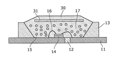
- FIG. 5 is a schematic cross-sectional view of a semiconductor light emitting device according to Embodiment 3 of the present invention.
- the quantum dot phosphor film 31 is placed in a transparent resin layer 30 made of a silicone resin formed on the resin layer 17 (first resin layer). (Second resin layer) is provided.
- the quantum dot phosphor film 31 was produced by forming a resin layer containing the quantum dot phosphor on the flexible transparent conductive substrate by electrodeposition.
- the quantum dot phosphor film 31 may be attached by performing thermosetting of the silicone resin in a state where the quantum dot phosphor film 31 is placed on the upper part of the resin layer 17 made of silicone resin, but the adhesion between the quantum dot phosphor film 31 and the silicone resin. In order to further increase the thickness, it is preferable to embed the quantum dot phosphor film 31 in the resin layer.
- the quantum dot phosphor film 31 is disposed on the resin layer 17, and the resin layer 30 made of silicone resin is injected again from the top of the quantum dot phosphor film 31 and thermally cured. .
- the quantum dot phosphor film (resin film) is not peeled off, and a highly reliable semiconductor light emitting device can be provided.
- the ceramic fine particles are contained in the resin layer 17 (first resin layer) as in the first embodiment.
- Thermal conductivity can be increased.
- the heat dissipation of the quantum dot fluorescent film 31 (2nd resin layer) can be improved, the temperature rise of the quantum dot fluorescent film 31 can be suppressed. Therefore, it can suppress that the quantum dot fluorescent substance (semiconductor microparticles
- Resin containing ceramic fine particles has increased thermal conductivity, so heat generated by the phosphor layer due to Stokes loss can be dissipated.
- the phosphor layer is affected by self-heating caused by LED operation. It becomes easy to receive.
- the junction temperature may exceed 100 ° C., which may accelerate the deterioration of the phosphor layer.
- the LED does not include ceramic fine particles in order to dissipate the heat generated in the phosphor layer to the conductive region of the lead frame and at the same time prevent the heat generated by the LED from being transmitted to the phosphor layer.
- FIG. 6 is a schematic cross-sectional view of a semiconductor light emitting device according to Embodiment 4 of the present invention.
- a resin is further interposed between the resin layer 17 (first resin layer) and the semiconductor light emitting element 14.
- a layer 40 (third resin layer) is formed.
- the resin layer 40 is a transparent resin layer that does not contain ceramic fine particles and is composed only of a transparent resin made of a silicone resin or the like.
- the semiconductor light emitting element 14 is enclosed in the resin layer 40.
- the resin layer 40 does not contain ceramic fine particles and has a lower thermal conductivity than the resin layer 17. As a result, since the heat of the semiconductor light emitting element 14 is shielded by the resin layer 40, the heat of the semiconductor light emitting element 14 is transmitted to the quantum dot phosphor layer 19 even when the semiconductor light emitting element 14 is operated at a high output. Can be suppressed. Thereby, the resin layer 17 can effectively suppress the temperature rise of the quantum dot phosphor layer 19.
- the heat dissipation of the quantum dot phosphor layer 19 is improved by the resin layer 17 (first resin layer) containing ceramic fine particles.
- the heat of the semiconductor light emitting element 14 can be shielded by the resin layer 40 (third resin layer) that does not contain ceramic fine particles.
- the resin layer 17 containing the ceramic fine particles 15 is in contact with the conductive region of the lead frame in order to secure a route for dissipating heat generated by the Stokes loss of the quantum dot phosphor layer 19. It is preferable. With this configuration, both the heat radiation of the quantum dot phosphor layer 19 and the heat shielding of the semiconductor light emitting element 14 can be further achieved, so that the quantum dot phosphor layer 19 can be used even during high output operation of the semiconductor light emitting element 14. Thus, it is possible to provide a semiconductor light emitting device that can effectively suppress the temperature rise and has higher reliability.
- FIG. 7 is an assembly process diagram of the semiconductor light emitting device according to Embodiment 4 of the present invention.
- the semiconductor light emitting device 14 (LED) is mounted on the lead frame 11 and wire bonding is performed (FIG. 7A), and only the semiconductor light emitting device 14 encloses a transparent resin layer 40 made of silicone resin. As shown in FIG. 7B, partial injection is performed.
- the defoaming treatment of the silicone resin is performed in the state shown in FIG.
- a thermosetting treatment is performed at 150 ° C. for 30 minutes to shape the silicone resin (resin layer 40).
- the quantum dot phosphor layer 19 is encapsulated.
- the glass plate 18 thus pressed is pressed from above to thermally cure the resin layer 17.
- the quantum dot phosphor may be mixed in a high thermal conductive silicone resin containing ceramic fine particles. Therefore, since the heat of the quantum dot phosphor due to Stokes loss is dissipated to the adjacent ceramic fine particles, it is possible to suppress the temperature rise of the quantum dot phosphor.
- the silicone resin has high oxygen permeability, there is a concern that the quantum dot phosphor is deteriorated by photooxidation.
- Quantum dot phosphors often have low chemical stability due to their small particle size and a large proportion of atoms occupying the surface. Especially in excited fluorescence under high temperature environment, photooxidation of the surface of the quantum dot phosphor The reaction proceeds and may cause a sudden decrease in luminous efficiency.
- the quantum dot aggregated fine particles are formed by coating the surface of an aggregate of one or more quantum dot phosphors with a transparent resin or inorganic coating having oxygen barrier properties and moisture resistance.
- the quantum dot aggregate fine particles and ceramic fine particles are mixed in a silicone resin.
- FIG. 8 is a schematic cross-sectional view of a semiconductor light emitting device according to Embodiment 5 of the present invention.
- the resin layer 17 is configured such that quantum dot aggregated fine particles 60 that are phosphors that convert wavelengths and ceramic fine particles 15 are dispersed and held in a transparent resin such as a silicone resin.
- the quantum dot aggregate fine particle 60 is composed of an aggregate of one or more quantum dot phosphors.
- the surface of the aggregate is covered with a material having oxygen barrier properties and moisture resistance.
- the aggregate is covered with a transparent acrylic resin film.
- the semiconductor light emitting element 14 is tightly covered with a resin layer 17.
- an acrylic resin film is used as the film of the quantum dot aggregate fine particles 60, but a transparent inorganic film such as a transparent silicon oxide (SiO 2 ) may be used.
- a transparent inorganic film such as a transparent silicon oxide (SiO 2 ) may be used.
- the heat dissipation of the quantum dot phosphor layer 19 (second resin layer) is improved by the resin layer 17 (first resin layer) containing the ceramic fine particles 15.
- the deterioration of the quantum dot phosphor due to photo-oxidation can be suppressed by an acrylic resin film that coats the surface of the quantum dot phosphor.
- a semiconductor light emitting device can be provided.
- the light emitted from the LED has the highest luminance directly above the LED, and the luminance around the LED tends to decrease. Therefore, the phosphor layer is not uniformly irradiated, causing uneven emission.
- white fine particles that reflect visible light are used as the ceramic fine particles 15 in the semiconductor light emitting devices in the first to fifth embodiments.
- the white fine particles can be used as the ceramic fine particles 15 in the semiconductor light emitting devices in the first to fifth embodiments.
- titanium oxide (TiO 2 ) can be used as the white fine particles.
- the ceramic fine particles 15 do not absorb the emission wavelength of the LED and the fluorescence wavelength of the quantum dot phosphor, but depending on the size of the fine particles, the LED light may be strongly reflected. In order to reflect light from the LED efficiently, it is desirable that the particle diameter of the light scattering fine particles is as large as the wavelength of the light.
- the constituent material of the ceramic fine particles 15 is transparent to the light of the LED, but when the size of the fine particles is about the wavelength, a light scattering phenomenon called Mie scattering occurs. For this reason, even fine particles made of a transparent material are scattered in white.
- the particles become even smaller, they become dominated by light scattering called Rayleigh scattering, and the scattering intensity is proportional to the sixth power of the particle diameter. Therefore, if the particles are too small, the particles are again transparent to the LED light. It becomes.
- the size of about one-quarter to one wavelength of the wavelength is necessary, and the white LED has a visible light region of 400 nm to 700 nm. Is preferably 100 nm to 700 nm.
- a particle size of 100 nm to 450 nm is desirable.
- TiO 2 is used as the white fine particles.
- lead basic carbonate (2PbCO 3 .Pb (OH) 2 ) called lead white
- ZnO zinc white
- CaSO 4 .2H 2 O calcium sulfate hydrate
- the ceramic fine particles 15 are composed of the white fine particles, the light of the semiconductor light emitting element 14 (LED) is scattered by the white fine particles and uniformly in the phosphor layer. Is irradiated. Therefore, it is possible to provide a semiconductor light emitting device free from light unevenness. Also in the present embodiment, the heat generated in the phosphor layer can be dissipated as in the first to fifth embodiments. Therefore, in the present embodiment, a semiconductor light emitting device that can achieve both uniform light emission and high heat dissipation can be provided. Also in this embodiment, the effect in each embodiment can be achieved.
- diamond fine particles are used as the ceramic fine particles 15 in the semiconductor light emitting devices of the first to sixth embodiments.
- Diamond is transparent to visible light and has a very high thermal conductivity. Therefore, only by dispersing a small amount of diamond fine particles in the silicone resin, the thermal conductivity of the resin layer 17 is greatly increased, and the heat dissipation of the phosphor layer (quantum dot phosphor layer, etc.) is improved.
- diamond fine particles are formed by chemical vapor deposition.
- the thermal conductivity of the diamond fine particles was about 1200 W / mK.
- a thermal conductivity of about 15 W / mK which is the same as that of the silicone resin containing 10 vol% of AlN fine particles, was obtained. This is about 100 times the thermal conductivity of a silicone resin that does not contain ceramic fine particles.
- the semiconductor light emitting device by using the diamond fine particles, the phosphor layer can be radiated with high efficiency, so that the temperature rise of the quantum dot phosphor is effectively suppressed. It is possible to provide a semiconductor light emitting device with high efficiency, high reliability, and high color rendering. Also in this embodiment, the effect in each embodiment can be achieved.
- the ceramic fine particles 15 may be a rare earth phosphor that absorbs light emitted from the semiconductor light emitting element 14 (LED) and emits excitation light of the quantum dot phosphor as fluorescence.
- a silicon aluminum oxynitride (SiAlON: Eu) phosphor to which europium ions that are rare earth phosphors are added is used as the ceramic fine particles 15 in the semiconductor light emitting devices of the first to sixth embodiments.
- the phosphor layer (quantum dot phosphor layer 19 or the like) contained a red quantum dot phosphor having a particle diameter that gives red fluorescence.
- the semiconductor light emitting element 14 is an LED that emits blue light
- part of the blue light emitted by the semiconductor light emitting element 14 is absorbed by the SiAlON (Eu phosphor) and gives green fluorescence.
- the red quantum dot phosphor absorbs part of the green light emission and gives red fluorescence.
- the quantum dot phosphor converts the wavelength from green to red.
- the Stokes loss is smaller than in the case of wavelength conversion from blue to red, and the calorific value of the quantum dot phosphor is reduced. Therefore, since the temperature rise of the quantum dots can be further suppressed, a highly reliable semiconductor light emitting device can be provided.
- the wavelength of the light of the semiconductor light emitting element is converted by the ceramic fine particles, so that a semiconductor light emitting device with high color rendering properties and high reliability can be provided. Also in this embodiment, the effect in each embodiment can be achieved.
- the semiconductor light emitting device according to the present invention has been described above based on the embodiment, but the present invention is not limited to the above embodiment.
- the ceramic fine particles 15 may be transparent fine particles that transmit visible light. Thereby, since the light of the semiconductor light emitting element 14 is irradiated to the phosphor layer without loss, a highly efficient semiconductor light emitting device can be provided.
- the present invention can realize a semiconductor light emitting device with high reliability, high efficiency, and high color rendering, it is widely useful in white LED light sources such as display devices and lighting devices.
Landscapes
- Led Device Packages (AREA)
Abstract
Le dispositif luminescent à semi-conducteurs de l'invention est équipé : d'un boîtier constitué de résine qui possède une partie en retrait; d'une grille de connexion (11) exposée sur la face fond de la partie en retrait; d'un élément luminescent à semi-conducteurs (14) placé sur la grille de connexion (11) située à l'intérieur de la partie en retrait; d'une couche de résine (17) formée de manière à être en contact avec la grille de connexion (11) à l'intérieur de la partie en retrait, et à couvrir la face fond; et d'une couche de phosphore à point quantique (19) formée sur la couche de résine (17) et l'élément luminescent à semi-conducteurs (14). La couche de résine (17) possède des microparticules de céramique (15). La couche de phosphore à point quantique (19) contient : des microparticules semi-conductrices possédant un spectre de fluorescence d'excitation qui diffère selon le diamètre des particules; et une résine dans laquelle les microparticules semi-conductrices sont dispersées et maintenues.
Priority Applications (3)
| Application Number | Priority Date | Filing Date | Title |
|---|---|---|---|
| CN2012800154155A CN103443941A (zh) | 2011-03-31 | 2012-03-01 | 半导体发光装置 |
| JP2013507111A JPWO2012132232A1 (ja) | 2011-03-31 | 2012-03-01 | 半導体発光装置 |
| US14/037,443 US20140021503A1 (en) | 2011-03-31 | 2013-09-26 | Semiconductor light emitting device |
Applications Claiming Priority (2)
| Application Number | Priority Date | Filing Date | Title |
|---|---|---|---|
| JP2011080740 | 2011-03-31 | ||
| JP2011-080740 | 2011-03-31 |
Related Child Applications (1)
| Application Number | Title | Priority Date | Filing Date |
|---|---|---|---|
| US14/037,443 Continuation US20140021503A1 (en) | 2011-03-31 | 2013-09-26 | Semiconductor light emitting device |
Publications (1)
| Publication Number | Publication Date |
|---|---|
| WO2012132232A1 true WO2012132232A1 (fr) | 2012-10-04 |
Family
ID=46930028
Family Applications (1)
| Application Number | Title | Priority Date | Filing Date |
|---|---|---|---|
| PCT/JP2012/001398 Ceased WO2012132232A1 (fr) | 2011-03-31 | 2012-03-01 | Dispositif luminescent à semi-conducteurs |
Country Status (4)
| Country | Link |
|---|---|
| US (1) | US20140021503A1 (fr) |
| JP (1) | JPWO2012132232A1 (fr) |
| CN (1) | CN103443941A (fr) |
| WO (1) | WO2012132232A1 (fr) |
Cited By (29)
| Publication number | Priority date | Publication date | Assignee | Title |
|---|---|---|---|---|
| CN103456865A (zh) * | 2013-09-03 | 2013-12-18 | 易美芯光(北京)科技有限公司 | 一种led封装 |
| WO2014112231A1 (fr) * | 2013-01-21 | 2014-07-24 | シャープ株式会社 | Dispositif électroluminescent, dispositif de guide de lumière, et procédé pour la fabrication de dispositif électroluminescent |
| WO2015004577A1 (fr) * | 2013-07-08 | 2015-01-15 | Koninklijke Philips N.V. | Dispositif électroluminescent à semi-conducteur à conversion de longueur d'onde |
| GB2523645A (en) * | 2014-01-23 | 2015-09-02 | Nanoco Technologies Ltd | Quantum dot chip on board |
| WO2015156227A1 (fr) * | 2014-04-08 | 2015-10-15 | Nsマテリアルズ株式会社 | Élément de conversion de longueur d'onde, corps moulé, dispositif de conversion de longueur d'onde, élément en feuille, dispositif électroluminescent, dispositif guide de lumière et dispositif d'affichage |
| WO2015190241A1 (fr) * | 2014-06-09 | 2015-12-17 | 日本電気硝子株式会社 | Dispositif luminescent |
| WO2015194297A1 (fr) * | 2014-06-18 | 2015-12-23 | 日本電気硝子株式会社 | Dispositif luminescent, et élément de conversion de longueur d'onde ainsi que procédé de fabrication de celui-ci |
| JP2016076634A (ja) * | 2014-10-08 | 2016-05-12 | エルジー ディスプレイ カンパニー リミテッド | Ledパッケージ、バックライトユニット及び液晶表示装置 |
| WO2016072311A1 (fr) * | 2014-11-04 | 2016-05-12 | Nsマテリアルズ株式会社 | Élément de conversion de longueur d'onde, et dispositif luminescent, organe luminescent, dispositif de source lumineuse ainsi que dispositif d'affichage mettant en œuvre celui-ci |
| WO2016075950A1 (fr) * | 2014-11-14 | 2016-05-19 | 富士フイルム株式会社 | Élément de conversion de longueur d'onde, unité de rétroéclairage en comportant, et appareil d'affichage à cristaux liquides |
| WO2016075949A1 (fr) * | 2014-11-14 | 2016-05-19 | 富士フイルム株式会社 | Élément de conversion de longueur d'onde, unité de rétroéclairage le comprenant et appareil d'affichage à cristaux liquides |
| JP2016103461A (ja) * | 2014-11-14 | 2016-06-02 | 富士フイルム株式会社 | 波長変換部材及びそれを備えたバックライトユニット、液晶表示装置 |
| JP2016102999A (ja) * | 2014-11-14 | 2016-06-02 | 富士フイルム株式会社 | 波長変換部材及びそれを備えたバックライトユニット、液晶表示装置 |
| WO2016104401A1 (fr) * | 2014-12-26 | 2016-06-30 | Nsマテリアルズ株式会社 | Élément de conversion de longueur d'onde et son procédé de fabrication |
| EP2940743A4 (fr) * | 2012-12-28 | 2016-07-27 | Konica Minolta Inc | Dispositif électroluminescent |
| JP2016162850A (ja) * | 2015-02-27 | 2016-09-05 | 豊田合成株式会社 | 発光装置 |
| JPWO2014073313A1 (ja) * | 2012-11-09 | 2016-09-08 | ソニー株式会社 | 照明装置および表示装置 |
| JP2016219748A (ja) * | 2015-05-26 | 2016-12-22 | シャープ株式会社 | 発光装置および画像表示装置 |
| JPWO2015194296A1 (ja) * | 2014-06-18 | 2017-04-20 | 日本電気硝子株式会社 | 発光デバイス |
| JP2017513230A (ja) * | 2014-04-04 | 2017-05-25 | コーニング精密素材株式会社Corning Precision Materials Co., Ltd. | 発光ダイオードの色変換用基板及びその製造方法 |
| WO2017163598A1 (fr) * | 2016-03-24 | 2017-09-28 | ソニー株式会社 | Dispositif électroluminescent, appareil d'affichage et appareil d'éclairage |
| WO2017169773A1 (fr) * | 2016-03-31 | 2017-10-05 | シャープ株式会社 | Source de lumière sans danger pour l'œil et son procédé de fabrication |
| JP2018037566A (ja) * | 2016-09-01 | 2018-03-08 | エルジー ディスプレイ カンパニー リミテッド | 光源装置および表示装置 |
| CN108922958A (zh) * | 2018-08-01 | 2018-11-30 | 苏州星烁纳米科技有限公司 | 白光led及显示装置 |
| JP2019054299A (ja) * | 2019-01-11 | 2019-04-04 | エルジー ディスプレイ カンパニー リミテッド | Ledパッケージ、バックライトユニット及び液晶表示装置 |
| JP2019087715A (ja) * | 2017-11-06 | 2019-06-06 | ルーメンス カンパニー リミテッド | Ledパッケージ |
| JP2022502832A (ja) * | 2018-09-27 | 2022-01-11 | ナージン テクノロジー コーポレーション リミテッドNajing Technology Corporation Limited | 発光素子の製造プロセス及び発光素子 |
| US20230359084A1 (en) * | 2020-04-09 | 2023-11-09 | Tcl China Star Optoelectronics Technology Co., Ltd. | Backlight module, display panel, and display device |
| JP2023172001A (ja) * | 2022-05-23 | 2023-12-06 | 日亜化学工業株式会社 | 波長変換部材及び発光装置並びに波長変換部材の製造方法 |
Families Citing this family (46)
| Publication number | Priority date | Publication date | Assignee | Title |
|---|---|---|---|---|
| CN103403892A (zh) * | 2011-03-31 | 2013-11-20 | 松下电器产业株式会社 | 半导体发光装置 |
| DE102011016567B4 (de) * | 2011-04-08 | 2023-05-11 | OSRAM Opto Semiconductors Gesellschaft mit beschränkter Haftung | Verfahren zum Herstellen eines optoelektronischen Bauelements und derart hergestelltes Bauelement |
| WO2013001687A1 (fr) * | 2011-06-30 | 2013-01-03 | パナソニック株式会社 | Dispositif émetteur de lumière |
| WO2013172847A1 (fr) * | 2012-05-17 | 2013-11-21 | Intel Corporation | Moulage d'insert de film pour la fabrication de dispositifs |
| JP2014056896A (ja) * | 2012-09-11 | 2014-03-27 | Ns Materials Kk | 半導体を利用した発光デバイス及びその製造方法 |
| JP2014112669A (ja) * | 2012-11-12 | 2014-06-19 | Citizen Holdings Co Ltd | 半導体発光装置及びその製造方法 |
| JP6476567B2 (ja) * | 2013-03-29 | 2019-03-06 | 日亜化学工業株式会社 | 発光装置 |
| JP6604543B2 (ja) * | 2013-08-09 | 2019-11-13 | 株式会社タムラ製作所 | 発光装置 |
| WO2015077369A1 (fr) * | 2013-11-19 | 2015-05-28 | Qd Vision, Inc. | Dispositif électroluminescent comprenant des points quantiques |
| TWI474519B (zh) * | 2013-12-12 | 2015-02-21 | Lextar Electronics Corp | 封裝材料及包含其之發光二極體的封裝結構 |
| WO2015121089A1 (fr) * | 2014-02-11 | 2015-08-20 | Koninklijke Philips N.V. | Élément convertisseur de longueur d'onde, module émetteur de lumière et luminaire |
| US9666771B2 (en) * | 2014-02-27 | 2017-05-30 | Koninklijke Philips N.V. | Method of forming a wavelength converted light emitting device |
| CN103869536B (zh) | 2014-03-06 | 2016-05-11 | 京东方科技集团股份有限公司 | 显示用基板及其制造方法、显示装置 |
| WO2015138495A1 (fr) * | 2014-03-11 | 2015-09-17 | Osram Sylvania Inc. | Ensembles convertisseurs optiques à dissipation thermique améliorée |
| WO2015175369A1 (fr) * | 2014-05-10 | 2015-11-19 | Sensor Electronic Technology, Inc. | Conditionnement pour dispositif optoélectronique à ultraviolets |
| US10147854B2 (en) | 2014-05-10 | 2018-12-04 | Sensor Electronic Technology, Inc. | Packaging for ultraviolet optoelectronic device |
| CN105093776B (zh) * | 2014-05-13 | 2020-08-25 | 深圳光峰科技股份有限公司 | 波长转换装置、光源系统及投影系统 |
| CN105280628B (zh) * | 2014-07-21 | 2018-08-10 | 中国科学院苏州纳米技术与纳米仿生研究所 | 基于透明基板的半导体发光器件封装结构 |
| CN105470374A (zh) * | 2014-09-05 | 2016-04-06 | 鸿富锦精密工业(深圳)有限公司 | 量子点封装结构及其制备方法 |
| JP6428089B2 (ja) * | 2014-09-24 | 2018-11-28 | 日亜化学工業株式会社 | 発光装置 |
| JP6457225B2 (ja) * | 2014-09-25 | 2019-01-23 | 株式会社小糸製作所 | 発光装置 |
| DE102014117764A1 (de) * | 2014-12-03 | 2016-06-09 | Osram Opto Semiconductors Gmbh | Strahlungsemittierendes optoelektronisches Halbleiterbauteil und Verfahren zu dessen Herstellung |
| CN104932142A (zh) * | 2015-06-10 | 2015-09-23 | 青岛海信电器股份有限公司 | 量子点发光器件及背光模组 |
| CN105185890A (zh) * | 2015-08-10 | 2015-12-23 | 深圳市华星光电技术有限公司 | Led光源结构及其封装方法 |
| JP6217711B2 (ja) * | 2015-08-21 | 2017-10-25 | 日亜化学工業株式会社 | 発光装置の製造方法 |
| CN105280789A (zh) * | 2015-09-18 | 2016-01-27 | 创维液晶器件(深圳)有限公司 | 一种量子点led |
| EP3147956B1 (fr) * | 2015-09-22 | 2023-05-03 | Samsung Electronics Co., Ltd. | Boîtier à del, unité de rétroéclairage et dispositif d'éclairage le comprenant, et dispositif d'affichage à cristaux liquides |
| US10627672B2 (en) | 2015-09-22 | 2020-04-21 | Samsung Electronics Co., Ltd. | LED package, backlight unit and illumination device including same, and liquid crystal display including backlight unit |
| DE102015118433A1 (de) | 2015-10-28 | 2017-05-04 | Osram Opto Semiconductors Gmbh | Optoelektronisches Bauelement und Verfahren zu seiner Herstellung |
| US20170125650A1 (en) * | 2015-11-02 | 2017-05-04 | Nanoco Technologies Ltd. | Display devices comprising green-emitting quantum dots and red KSF phosphor |
| ITUB20155681A1 (it) * | 2015-11-18 | 2017-05-18 | St Microelectronics Srl | Dispositivo elettronico resistente a radiazioni e metodo per proteggere un dispositivo elettronico da radiazioni ionizzanti |
| DE102016103463A1 (de) * | 2016-02-26 | 2017-08-31 | Osram Opto Semiconductors Gmbh | Optoelektronisches Bauelement und Verfahren zur Herstellung eines optoelektronischen Bauelements |
| WO2017188191A1 (fr) * | 2016-04-25 | 2017-11-02 | 日本特殊陶業株式会社 | Élément de conversion de longueur d'onde, son procédé de fabrication, et dispositif électroluminescent |
| JP6493345B2 (ja) * | 2016-09-16 | 2019-04-03 | 日亜化学工業株式会社 | 発光装置 |
| DE102017108573A1 (de) * | 2017-04-21 | 2018-10-25 | Osram Opto Semiconductors Gmbh | Optoelektronisches Bauelement und Verfahren zur Herstellung eines optoelektronischen Bauelements |
| US10475967B2 (en) * | 2017-04-27 | 2019-11-12 | Osram Opto Semiconductors Gmbh | Wavelength converters with improved thermal conductivity and lighting devices including the same |
| KR102389815B1 (ko) * | 2017-06-05 | 2022-04-22 | 삼성전자주식회사 | 양자점 유리셀 및 이를 포함하는 발광소자 패키지 |
| JP2019049619A (ja) * | 2017-09-08 | 2019-03-28 | セイコーエプソン株式会社 | 波長変換素子、光源装置およびプロジェクター |
| KR102401826B1 (ko) * | 2017-09-15 | 2022-05-25 | 쑤저우 레킨 세미컨덕터 컴퍼니 리미티드 | 발광소자 패키지 및 이를 포함하는 조명장치 |
| US10854554B2 (en) * | 2018-01-23 | 2020-12-01 | Ferro Corporation | Carbide, nitride and silicide enhancers for laser absorption |
| CN108615742A (zh) * | 2018-07-10 | 2018-10-02 | 南方科技大学 | 一种显示面板制作方法、显示面板及显示装置 |
| JP6940775B2 (ja) * | 2018-10-30 | 2021-09-29 | 日亜化学工業株式会社 | 発光装置の製造方法 |
| CN109445191B (zh) * | 2019-01-02 | 2022-05-13 | 京东方科技集团股份有限公司 | 发光件及其制作方法、背光源和显示装置 |
| KR102917099B1 (ko) * | 2020-06-30 | 2026-01-22 | 엘지디스플레이 주식회사 | 표시장치 및 그 제조방법 |
| JP3250506U (ja) * | 2022-03-31 | 2025-03-11 | シェンツェン ジュフェイ オプトエレクトロニクス カンパニー リミテッド | Ledデバイス |
| TWI853645B (zh) * | 2023-07-14 | 2024-08-21 | 錼創顯示科技股份有限公司 | 顯示面板及其製造方法 |
Citations (11)
| Publication number | Priority date | Publication date | Assignee | Title |
|---|---|---|---|---|
| JPH1168237A (ja) * | 1997-08-13 | 1999-03-09 | Sony Corp | 半導体発光装置および半導体装置 |
| JP2004071908A (ja) * | 2002-08-07 | 2004-03-04 | Matsushita Electric Works Ltd | 発光装置 |
| JP2005197476A (ja) * | 2004-01-07 | 2005-07-21 | Koito Mfg Co Ltd | 発光モジュール及び車両用灯具 |
| JP2006054313A (ja) * | 2004-08-11 | 2006-02-23 | Rohm Co Ltd | 半導体発光装置 |
| JP2007067204A (ja) * | 2005-08-31 | 2007-03-15 | Toshiba Lighting & Technology Corp | 発光ダイオード装置 |
| JP2007149909A (ja) * | 2005-11-28 | 2007-06-14 | Nichia Chem Ind Ltd | 発光装置 |
| JP2007294890A (ja) * | 2006-03-31 | 2007-11-08 | Toshiba Lighting & Technology Corp | 発光装置 |
| JP2008192909A (ja) * | 2007-02-06 | 2008-08-21 | Stanley Electric Co Ltd | 発光装置およびその製造方法 |
| WO2008108266A1 (fr) * | 2007-03-06 | 2008-09-12 | Konica Minolta Medical & Graphic, Inc. | Procédé de fabrication de nanoparticules semi-conductrices, procédé de fabrication de nanoparticules semi-conductrices cœur-écorce, et nanoparticules semi-conductrices cœur-écorce |
| JP2009071005A (ja) * | 2007-09-13 | 2009-04-02 | Sony Corp | 波長変換部材及びその製造方法、並びに、波長変換部材を用いた発光デバイス |
| JP2009206459A (ja) * | 2008-02-29 | 2009-09-10 | Sharp Corp | 色変換部材およびそれを用いた発光装置 |
Family Cites Families (15)
| Publication number | Priority date | Publication date | Assignee | Title |
|---|---|---|---|---|
| KR100265859B1 (ko) * | 1996-12-21 | 2000-09-15 | 정선종 | 전계방출 디스플레이용 발광입자 |
| US20020084745A1 (en) * | 2000-12-29 | 2002-07-04 | Airma Optoelectronics Corporation | Light emitting diode with light conversion by dielectric phosphor powder |
| US7868343B2 (en) * | 2004-04-06 | 2011-01-11 | Cree, Inc. | Light-emitting devices having multiple encapsulation layers with at least one of the encapsulation layers including nanoparticles and methods of forming the same |
| JP2006135002A (ja) * | 2004-11-04 | 2006-05-25 | Koito Mfg Co Ltd | 発光デバイス及び車両用灯具 |
| US20080173886A1 (en) * | 2006-05-11 | 2008-07-24 | Evident Technologies, Inc. | Solid state lighting devices comprising quantum dots |
| KR100901947B1 (ko) * | 2006-07-14 | 2009-06-10 | 삼성전자주식회사 | 반도체 나노결정을 이용하는 백색 발광 다이오드 및 그의제조방법 |
| CN101364626B (zh) * | 2007-08-07 | 2010-09-29 | 亿光电子工业股份有限公司 | 发光二极管装置 |
| CN101609863B (zh) * | 2008-06-16 | 2013-01-02 | 启萌科技有限公司 | 荧光膜 |
| CN100565000C (zh) * | 2008-08-11 | 2009-12-02 | 山东华光光电子有限公司 | 利用yag透明陶瓷制备白光led的方法 |
| KR100982991B1 (ko) * | 2008-09-03 | 2010-09-17 | 삼성엘이디 주식회사 | 양자점 파장변환체, 양자점 파장변환체의 제조방법 및 양자점 파장변환체를 포함하는 발광장치 |
| JP5744386B2 (ja) * | 2009-10-07 | 2015-07-08 | 日東電工株式会社 | 光半導体封止材 |
| JP2011082339A (ja) * | 2009-10-07 | 2011-04-21 | Nitto Denko Corp | 光半導体封止用キット |
| JP5749327B2 (ja) * | 2010-03-19 | 2015-07-15 | 日東電工株式会社 | 発光装置用ガーネット系蛍光体セラミックシート |
| JP5249283B2 (ja) * | 2010-05-10 | 2013-07-31 | デクセリアルズ株式会社 | 緑色発光蛍光体粒子及びその製造方法、並びに、色変換シート、発光装置及び画像表示装置組立体 |
| US8294168B2 (en) * | 2010-06-04 | 2012-10-23 | Samsung Electronics Co., Ltd. | Light source module using quantum dots, backlight unit employing the light source module, display apparatus, and illumination apparatus |
-
2012
- 2012-03-01 JP JP2013507111A patent/JPWO2012132232A1/ja active Pending
- 2012-03-01 WO PCT/JP2012/001398 patent/WO2012132232A1/fr not_active Ceased
- 2012-03-01 CN CN2012800154155A patent/CN103443941A/zh active Pending
-
2013
- 2013-09-26 US US14/037,443 patent/US20140021503A1/en not_active Abandoned
Patent Citations (11)
| Publication number | Priority date | Publication date | Assignee | Title |
|---|---|---|---|---|
| JPH1168237A (ja) * | 1997-08-13 | 1999-03-09 | Sony Corp | 半導体発光装置および半導体装置 |
| JP2004071908A (ja) * | 2002-08-07 | 2004-03-04 | Matsushita Electric Works Ltd | 発光装置 |
| JP2005197476A (ja) * | 2004-01-07 | 2005-07-21 | Koito Mfg Co Ltd | 発光モジュール及び車両用灯具 |
| JP2006054313A (ja) * | 2004-08-11 | 2006-02-23 | Rohm Co Ltd | 半導体発光装置 |
| JP2007067204A (ja) * | 2005-08-31 | 2007-03-15 | Toshiba Lighting & Technology Corp | 発光ダイオード装置 |
| JP2007149909A (ja) * | 2005-11-28 | 2007-06-14 | Nichia Chem Ind Ltd | 発光装置 |
| JP2007294890A (ja) * | 2006-03-31 | 2007-11-08 | Toshiba Lighting & Technology Corp | 発光装置 |
| JP2008192909A (ja) * | 2007-02-06 | 2008-08-21 | Stanley Electric Co Ltd | 発光装置およびその製造方法 |
| WO2008108266A1 (fr) * | 2007-03-06 | 2008-09-12 | Konica Minolta Medical & Graphic, Inc. | Procédé de fabrication de nanoparticules semi-conductrices, procédé de fabrication de nanoparticules semi-conductrices cœur-écorce, et nanoparticules semi-conductrices cœur-écorce |
| JP2009071005A (ja) * | 2007-09-13 | 2009-04-02 | Sony Corp | 波長変換部材及びその製造方法、並びに、波長変換部材を用いた発光デバイス |
| JP2009206459A (ja) * | 2008-02-29 | 2009-09-10 | Sharp Corp | 色変換部材およびそれを用いた発光装置 |
Cited By (70)
| Publication number | Priority date | Publication date | Assignee | Title |
|---|---|---|---|---|
| US11977298B2 (en) | 2012-11-09 | 2024-05-07 | Saturn Licensing Llc | Illumination device and display device |
| JPWO2014073313A1 (ja) * | 2012-11-09 | 2016-09-08 | ソニー株式会社 | 照明装置および表示装置 |
| US11693277B2 (en) | 2012-11-09 | 2023-07-04 | Saturn Licensing Llc | Illumination device and display device |
| US12504660B2 (en) | 2012-11-09 | 2025-12-23 | Saturn Licensing Llc | Illumination device and display device |
| US11340498B2 (en) | 2012-11-09 | 2022-05-24 | Saturn Licensing, Llc | Illumination device and display device |
| US10240750B2 (en) | 2012-11-09 | 2019-03-26 | Saturn Licensing Llc | Illumination device and display device |
| US9885462B2 (en) | 2012-11-09 | 2018-02-06 | Saturn Licensing Llc | Illumination device and display device |
| US10838257B2 (en) | 2012-11-09 | 2020-11-17 | Saturn Licensing Llc | Illumination device and display device |
| US10480753B2 (en) | 2012-11-09 | 2019-11-19 | Saturn Licensing Llc | Illumination device and display device |
| EP2940743A4 (fr) * | 2012-12-28 | 2016-07-27 | Konica Minolta Inc | Dispositif électroluminescent |
| WO2014112231A1 (fr) * | 2013-01-21 | 2014-07-24 | シャープ株式会社 | Dispositif électroluminescent, dispositif de guide de lumière, et procédé pour la fabrication de dispositif électroluminescent |
| US9761768B2 (en) | 2013-07-08 | 2017-09-12 | Koninklijke Philips N.V. | Wavelength converted semiconductor light emitting device |
| US10790417B2 (en) | 2013-07-08 | 2020-09-29 | Lumileds Llc | Wavelength converted semiconductor light emitting device |
| US10270013B2 (en) | 2013-07-08 | 2019-04-23 | Lumileds Llc | Wavelength converted semiconductor light emitting device |
| WO2015004577A1 (fr) * | 2013-07-08 | 2015-01-15 | Koninklijke Philips N.V. | Dispositif électroluminescent à semi-conducteur à conversion de longueur d'onde |
| CN103456865A (zh) * | 2013-09-03 | 2013-12-18 | 易美芯光(北京)科技有限公司 | 一种led封装 |
| US9634198B2 (en) | 2014-01-23 | 2017-04-25 | Nanoco Technologies Ltd. | Quantum dot chip on board |
| GB2523645B (en) * | 2014-01-23 | 2018-10-17 | Nanoco Tech Limited | Quantum dot chip on board LEDs |
| GB2523645A (en) * | 2014-01-23 | 2015-09-02 | Nanoco Technologies Ltd | Quantum dot chip on board |
| JP2017513230A (ja) * | 2014-04-04 | 2017-05-25 | コーニング精密素材株式会社Corning Precision Materials Co., Ltd. | 発光ダイオードの色変換用基板及びその製造方法 |
| US10436418B2 (en) | 2014-04-08 | 2019-10-08 | Ns Materials Inc. | Wavelength conversion member, molded body, wavelength conversion apparatus, sheet member, light emitting apparatus, light guide apparatus and display apparatus |
| US10101008B2 (en) | 2014-04-08 | 2018-10-16 | Ns Materials Inc. | Wavelength conversion member, molded body, wavelength conversion apparatus, sheet member, light emitting apparatus, light guide apparatus and display apparatus |
| JP2020043353A (ja) * | 2014-04-08 | 2020-03-19 | Nsマテリアルズ株式会社 | 波長変換部材、成形体、波長変換装置、シート部材、発光装置、導光装置、並びに表示装置 |
| JPWO2015156227A1 (ja) * | 2014-04-08 | 2017-04-13 | Nsマテリアルズ株式会社 | 波長変換部材、成形体、波長変換装置、シート部材、発光装置、導光装置、並びに表示装置 |
| US10670230B2 (en) | 2014-04-08 | 2020-06-02 | Ns Materials Inc. | Wavelength conversion member, molded body, wavelength conversion apparatus, sheet member, light emitting apparatus, light guide apparatus and display apparatus |
| WO2015156227A1 (fr) * | 2014-04-08 | 2015-10-15 | Nsマテリアルズ株式会社 | Élément de conversion de longueur d'onde, corps moulé, dispositif de conversion de longueur d'onde, élément en feuille, dispositif électroluminescent, dispositif guide de lumière et dispositif d'affichage |
| US9859479B2 (en) | 2014-06-09 | 2018-01-02 | Nippon Electric Glass Co., Ltd | Light-emitting device including quantum dots |
| JP2015233057A (ja) * | 2014-06-09 | 2015-12-24 | 日本電気硝子株式会社 | 発光デバイス |
| WO2015190241A1 (fr) * | 2014-06-09 | 2015-12-17 | 日本電気硝子株式会社 | Dispositif luminescent |
| JPWO2015194296A1 (ja) * | 2014-06-18 | 2017-04-20 | 日本電気硝子株式会社 | 発光デバイス |
| WO2015194297A1 (fr) * | 2014-06-18 | 2015-12-23 | 日本電気硝子株式会社 | Dispositif luminescent, et élément de conversion de longueur d'onde ainsi que procédé de fabrication de celui-ci |
| US10573792B2 (en) | 2014-10-08 | 2020-02-25 | Lg Display Co., Ltd. | LED package, backlight unit and liquid crystal display device |
| JP2016076634A (ja) * | 2014-10-08 | 2016-05-12 | エルジー ディスプレイ カンパニー リミテッド | Ledパッケージ、バックライトユニット及び液晶表示装置 |
| JPWO2016072311A1 (ja) * | 2014-11-04 | 2017-08-24 | Nsマテリアルズ株式会社 | 波長変換部材、及びそれを用いた発光装置、発光素子、光源装置、並びに表示装置 |
| US10422937B2 (en) | 2014-11-04 | 2019-09-24 | Ns Materials Inc. | Wavelength converting member, and light emitting device, light emitting element, light source unit, and display device using wavelength converting member |
| WO2016072311A1 (fr) * | 2014-11-04 | 2016-05-12 | Nsマテリアルズ株式会社 | Élément de conversion de longueur d'onde, et dispositif luminescent, organe luminescent, dispositif de source lumineuse ainsi que dispositif d'affichage mettant en œuvre celui-ci |
| WO2016075949A1 (fr) * | 2014-11-14 | 2016-05-19 | 富士フイルム株式会社 | Élément de conversion de longueur d'onde, unité de rétroéclairage le comprenant et appareil d'affichage à cristaux liquides |
| JP2016102999A (ja) * | 2014-11-14 | 2016-06-02 | 富士フイルム株式会社 | 波長変換部材及びそれを備えたバックライトユニット、液晶表示装置 |
| JP2016103461A (ja) * | 2014-11-14 | 2016-06-02 | 富士フイルム株式会社 | 波長変換部材及びそれを備えたバックライトユニット、液晶表示装置 |
| WO2016075950A1 (fr) * | 2014-11-14 | 2016-05-19 | 富士フイルム株式会社 | Élément de conversion de longueur d'onde, unité de rétroéclairage en comportant, et appareil d'affichage à cristaux liquides |
| US11316082B2 (en) | 2014-12-26 | 2022-04-26 | Ns Materials Inc. | Wavelength converting member and method of producing the same |
| WO2016104401A1 (fr) * | 2014-12-26 | 2016-06-30 | Nsマテリアルズ株式会社 | Élément de conversion de longueur d'onde et son procédé de fabrication |
| JP2016162850A (ja) * | 2015-02-27 | 2016-09-05 | 豊田合成株式会社 | 発光装置 |
| JP2016219748A (ja) * | 2015-05-26 | 2016-12-22 | シャープ株式会社 | 発光装置および画像表示装置 |
| JPWO2017163598A1 (ja) * | 2016-03-24 | 2019-01-31 | ソニー株式会社 | 発光装置、表示装置および照明装置 |
| JP2024098979A (ja) * | 2016-03-24 | 2024-07-24 | サターン ライセンシング エルエルシー | 発光装置、表示装置および照明装置 |
| WO2017163598A1 (fr) * | 2016-03-24 | 2017-09-28 | ソニー株式会社 | Dispositif électroluminescent, appareil d'affichage et appareil d'éclairage |
| JP7770455B2 (ja) | 2016-03-24 | 2025-11-14 | サターン ライセンシング エルエルシー | 発光装置、表示装置および照明装置 |
| US10877346B2 (en) | 2016-03-24 | 2020-12-29 | Saturn Licensing Llc | Light-emitting device, display apparatus, and illumination apparatus |
| US12386221B2 (en) | 2016-03-24 | 2025-08-12 | Saturn Licensing Llc | Light-emitting device, display apparatus, and illumination apparatus |
| US12372827B2 (en) | 2016-03-24 | 2025-07-29 | Saturn Licensing Llc | Light-emitting device, display apparatus, and illumination apparatus |
| US11294228B2 (en) | 2016-03-24 | 2022-04-05 | Saturn Licensing Llc | Light-emitting device, display apparatus, and illumination apparatus |
| JP7466620B2 (ja) | 2016-03-24 | 2024-04-12 | サターン ライセンシング エルエルシー | 発光装置、表示装置および照明装置 |
| US11630344B2 (en) | 2016-03-24 | 2023-04-18 | Saturn Licensing Llc | Light-emitting device, display apparatus, and illumination apparatus |
| JP2023038217A (ja) * | 2016-03-24 | 2023-03-16 | ソニーグループ株式会社 | 発光装置、表示装置および照明装置 |
| JPWO2017169773A1 (ja) * | 2016-03-31 | 2018-11-29 | シャープ株式会社 | アイセーフ光源、およびその製造方法 |
| WO2017169773A1 (fr) * | 2016-03-31 | 2017-10-05 | シャープ株式会社 | Source de lumière sans danger pour l'œil et son procédé de fabrication |
| JP2018037566A (ja) * | 2016-09-01 | 2018-03-08 | エルジー ディスプレイ カンパニー リミテッド | 光源装置および表示装置 |
| JP7029882B2 (ja) | 2016-09-01 | 2022-03-04 | エルジー ディスプレイ カンパニー リミテッド | 光源装置および表示装置 |
| JP2019087715A (ja) * | 2017-11-06 | 2019-06-06 | ルーメンス カンパニー リミテッド | Ledパッケージ |
| US10586897B2 (en) | 2017-11-06 | 2020-03-10 | Lumens Co., Ltd. | LED package |
| CN108922958B (zh) * | 2018-08-01 | 2024-03-15 | 苏州星烁纳米科技有限公司 | 白光led及显示装置 |
| CN108922958A (zh) * | 2018-08-01 | 2018-11-30 | 苏州星烁纳米科技有限公司 | 白光led及显示装置 |
| JP2022502832A (ja) * | 2018-09-27 | 2022-01-11 | ナージン テクノロジー コーポレーション リミテッドNajing Technology Corporation Limited | 発光素子の製造プロセス及び発光素子 |
| JP7218950B2 (ja) | 2018-09-27 | 2023-02-07 | ナージン テクノロジー コーポレーション リミテッド | 発光素子の製造プロセス及び発光素子 |
| JP2019054299A (ja) * | 2019-01-11 | 2019-04-04 | エルジー ディスプレイ カンパニー リミテッド | Ledパッケージ、バックライトユニット及び液晶表示装置 |
| US20230359084A1 (en) * | 2020-04-09 | 2023-11-09 | Tcl China Star Optoelectronics Technology Co., Ltd. | Backlight module, display panel, and display device |
| US12078889B2 (en) * | 2020-04-09 | 2024-09-03 | Tcl China Star Optoelectronics Technology Co., Ltd. | Backlight module, display panel, and display device |
| JP2023172001A (ja) * | 2022-05-23 | 2023-12-06 | 日亜化学工業株式会社 | 波長変換部材及び発光装置並びに波長変換部材の製造方法 |
| JP7801580B2 (ja) | 2022-05-23 | 2026-01-19 | 日亜化学工業株式会社 | 波長変換部材及び発光装置並びに波長変換部材の製造方法 |
Also Published As
| Publication number | Publication date |
|---|---|
| JPWO2012132232A1 (ja) | 2014-07-24 |
| US20140021503A1 (en) | 2014-01-23 |
| CN103443941A (zh) | 2013-12-11 |
Similar Documents
| Publication | Publication Date | Title |
|---|---|---|
| WO2012132232A1 (fr) | Dispositif luminescent à semi-conducteurs | |
| US11688842B2 (en) | Light emitting diodes with enhanced thermal sinking and associated methods of operation | |
| CN100533795C (zh) | 发光装置 | |
| JP5777705B2 (ja) | 発光装置及びその製造方法 | |
| EP2434554B1 (fr) | Dispositif électroluminescent converti en longueur d'onde et à émission uniforme | |
| JP5113820B2 (ja) | 発光装置 | |
| US7906892B2 (en) | Light emitting device | |
| WO2012131792A1 (fr) | Dispositif luminescent à semi-conducteurs | |
| JP2004056075A (ja) | 発光装置およびその製造方法 | |
| JP2012531043A (ja) | 蛍光体変換赤外線led関連アプリケーション | |
| JP6686081B2 (ja) | 量子ドットに基づいて色変換する発光装置、および、その製造方法 | |
| JP2013216800A5 (ja) | 波長変換用無機成形体及びその製造方法、並びに発光装置 | |
| WO2011004795A1 (fr) | Dispositif électroluminescent | |
| CN106195925A (zh) | 一种波长转换装置、发光装置及投影装置 | |
| JP2014072213A (ja) | 発光装置及びその製造方法 | |
| JP4417906B2 (ja) | 発光装置及びその製造方法 | |
| JP2014067774A (ja) | 波長変換部材及び波長変換部材を用いた半導体発光装置 | |
| CN108110120A (zh) | 量子点led以及显示装置 | |
| CN112166354A (zh) | 波长转换元件以及光源装置 | |
| CN103972366A (zh) | 波长转换物质、波长转换胶体以及发光装置 | |
| JP2011159770A (ja) | 白色半導体発光装置 | |
| JP6743630B2 (ja) | 発光装置およびその製造方法 | |
| KR20210100057A (ko) | 발광 장치 | |
| CN110361912B (zh) | 波长转换装置 | |
| JPWO2018212300A1 (ja) | 発光装置 |
Legal Events
| Date | Code | Title | Description |
|---|---|---|---|
| 121 | Ep: the epo has been informed by wipo that ep was designated in this application |
Ref document number: 12763616 Country of ref document: EP Kind code of ref document: A1 |
|
| ENP | Entry into the national phase |
Ref document number: 2013507111 Country of ref document: JP Kind code of ref document: A |
|
| NENP | Non-entry into the national phase |
Ref country code: DE |
|
| 122 | Ep: pct application non-entry in european phase |
Ref document number: 12763616 Country of ref document: EP Kind code of ref document: A1 |