WO2012132385A1 - 光電場増強デバイスの製造方法 - Google Patents
光電場増強デバイスの製造方法 Download PDFInfo
- Publication number
- WO2012132385A1 WO2012132385A1 PCT/JP2012/002072 JP2012002072W WO2012132385A1 WO 2012132385 A1 WO2012132385 A1 WO 2012132385A1 JP 2012002072 W JP2012002072 W JP 2012002072W WO 2012132385 A1 WO2012132385 A1 WO 2012132385A1
- Authority
- WO
- WIPO (PCT)
- Prior art keywords
- metal
- convex structure
- layer
- photoelectric field
- field enhancement
- Prior art date
- Legal status (The legal status is an assumption and is not a legal conclusion. Google has not performed a legal analysis and makes no representation as to the accuracy of the status listed.)
- Ceased
Links
Images






Classifications
-
- G—PHYSICS
- G01—MEASURING; TESTING
- G01N—INVESTIGATING OR ANALYSING MATERIALS BY DETERMINING THEIR CHEMICAL OR PHYSICAL PROPERTIES
- G01N21/00—Investigating or analysing materials by the use of optical means, i.e. using sub-millimetre waves, infrared, visible or ultraviolet light
- G01N21/62—Systems in which the material investigated is excited whereby it emits light or causes a change in wavelength of the incident light
- G01N21/63—Systems in which the material investigated is excited whereby it emits light or causes a change in wavelength of the incident light optically excited
- G01N21/65—Raman scattering
- G01N21/658—Raman scattering enhancement Raman, e.g. surface plasmons
-
- G—PHYSICS
- G01—MEASURING; TESTING
- G01J—MEASUREMENT OF INTENSITY, VELOCITY, SPECTRAL CONTENT, POLARISATION, PHASE OR PULSE CHARACTERISTICS OF INFRARED, VISIBLE OR ULTRAVIOLET LIGHT; COLORIMETRY; RADIATION PYROMETRY
- G01J3/00—Spectrometry; Spectrophotometry; Monochromators; Measuring colours
- G01J3/28—Investigating the spectrum
- G01J3/44—Raman spectrometry; Scattering spectrometry ; Fluorescence spectrometry
-
- C—CHEMISTRY; METALLURGY
- C03—GLASS; MINERAL OR SLAG WOOL
- C03C—CHEMICAL COMPOSITION OF GLASSES, GLAZES OR VITREOUS ENAMELS; SURFACE TREATMENT OF GLASS; SURFACE TREATMENT OF FIBRES OR FILAMENTS MADE FROM GLASS, MINERALS OR SLAGS; JOINING GLASS TO GLASS OR OTHER MATERIALS
- C03C17/00—Surface treatment of glass, not in the form of fibres or filaments, by coating
- C03C17/06—Surface treatment of glass, not in the form of fibres or filaments, by coating with metals
- C03C17/09—Surface treatment of glass, not in the form of fibres or filaments, by coating with metals by deposition from the vapour phase
-
- C—CHEMISTRY; METALLURGY
- C23—COATING METALLIC MATERIAL; COATING MATERIAL WITH METALLIC MATERIAL; CHEMICAL SURFACE TREATMENT; DIFFUSION TREATMENT OF METALLIC MATERIAL; COATING BY VACUUM EVAPORATION, BY SPUTTERING, BY ION IMPLANTATION OR BY CHEMICAL VAPOUR DEPOSITION, IN GENERAL; INHIBITING CORROSION OF METALLIC MATERIAL OR INCRUSTATION IN GENERAL
- C23C—COATING METALLIC MATERIAL; COATING MATERIAL WITH METALLIC MATERIAL; SURFACE TREATMENT OF METALLIC MATERIAL BY DIFFUSION INTO THE SURFACE, BY CHEMICAL CONVERSION OR SUBSTITUTION; COATING BY VACUUM EVAPORATION, BY SPUTTERING, BY ION IMPLANTATION OR BY CHEMICAL VAPOUR DEPOSITION, IN GENERAL
- C23C14/00—Coating by vacuum evaporation, by sputtering or by ion implantation of the coating forming material
- C23C14/06—Coating by vacuum evaporation, by sputtering or by ion implantation of the coating forming material characterised by the coating material
- C23C14/14—Metallic material, boron or silicon
- C23C14/18—Metallic material, boron or silicon on other inorganic substrates
-
- C—CHEMISTRY; METALLURGY
- C23—COATING METALLIC MATERIAL; COATING MATERIAL WITH METALLIC MATERIAL; CHEMICAL SURFACE TREATMENT; DIFFUSION TREATMENT OF METALLIC MATERIAL; COATING BY VACUUM EVAPORATION, BY SPUTTERING, BY ION IMPLANTATION OR BY CHEMICAL VAPOUR DEPOSITION, IN GENERAL; INHIBITING CORROSION OF METALLIC MATERIAL OR INCRUSTATION IN GENERAL
- C23C—COATING METALLIC MATERIAL; COATING MATERIAL WITH METALLIC MATERIAL; SURFACE TREATMENT OF METALLIC MATERIAL BY DIFFUSION INTO THE SURFACE, BY CHEMICAL CONVERSION OR SUBSTITUTION; COATING BY VACUUM EVAPORATION, BY SPUTTERING, BY ION IMPLANTATION OR BY CHEMICAL VAPOUR DEPOSITION, IN GENERAL
- C23C14/00—Coating by vacuum evaporation, by sputtering or by ion implantation of the coating forming material
- C23C14/58—After-treatment
- C23C14/5846—Reactive treatment
- C23C14/5853—Oxidation
-
- C—CHEMISTRY; METALLURGY
- C23—COATING METALLIC MATERIAL; COATING MATERIAL WITH METALLIC MATERIAL; CHEMICAL SURFACE TREATMENT; DIFFUSION TREATMENT OF METALLIC MATERIAL; COATING BY VACUUM EVAPORATION, BY SPUTTERING, BY ION IMPLANTATION OR BY CHEMICAL VAPOUR DEPOSITION, IN GENERAL; INHIBITING CORROSION OF METALLIC MATERIAL OR INCRUSTATION IN GENERAL
- C23C—COATING METALLIC MATERIAL; COATING MATERIAL WITH METALLIC MATERIAL; SURFACE TREATMENT OF METALLIC MATERIAL BY DIFFUSION INTO THE SURFACE, BY CHEMICAL CONVERSION OR SUBSTITUTION; COATING BY VACUUM EVAPORATION, BY SPUTTERING, BY ION IMPLANTATION OR BY CHEMICAL VAPOUR DEPOSITION, IN GENERAL
- C23C28/00—Coating for obtaining at least two superposed coatings either by methods not provided for in a single one of groups C23C2/00 - C23C26/00 or by combinations of methods provided for in subclasses C23C and C25C or C25D
- C23C28/30—Coatings combining at least one metallic layer and at least one inorganic non-metallic layer
- C23C28/32—Coatings combining at least one metallic layer and at least one inorganic non-metallic layer including at least one pure metallic layer
- C23C28/322—Coatings combining at least one metallic layer and at least one inorganic non-metallic layer including at least one pure metallic layer only coatings of metal elements only
-
- C—CHEMISTRY; METALLURGY
- C23—COATING METALLIC MATERIAL; COATING MATERIAL WITH METALLIC MATERIAL; CHEMICAL SURFACE TREATMENT; DIFFUSION TREATMENT OF METALLIC MATERIAL; COATING BY VACUUM EVAPORATION, BY SPUTTERING, BY ION IMPLANTATION OR BY CHEMICAL VAPOUR DEPOSITION, IN GENERAL; INHIBITING CORROSION OF METALLIC MATERIAL OR INCRUSTATION IN GENERAL
- C23C—COATING METALLIC MATERIAL; COATING MATERIAL WITH METALLIC MATERIAL; SURFACE TREATMENT OF METALLIC MATERIAL BY DIFFUSION INTO THE SURFACE, BY CHEMICAL CONVERSION OR SUBSTITUTION; COATING BY VACUUM EVAPORATION, BY SPUTTERING, BY ION IMPLANTATION OR BY CHEMICAL VAPOUR DEPOSITION, IN GENERAL
- C23C28/00—Coating for obtaining at least two superposed coatings either by methods not provided for in a single one of groups C23C2/00 - C23C26/00 or by combinations of methods provided for in subclasses C23C and C25C or C25D
- C23C28/30—Coatings combining at least one metallic layer and at least one inorganic non-metallic layer
- C23C28/34—Coatings combining at least one metallic layer and at least one inorganic non-metallic layer including at least one inorganic non-metallic material layer, e.g. metal carbide, nitride, boride, silicide layer and their mixtures, enamels, phosphates and sulphates
- C23C28/345—Coatings combining at least one metallic layer and at least one inorganic non-metallic layer including at least one inorganic non-metallic material layer, e.g. metal carbide, nitride, boride, silicide layer and their mixtures, enamels, phosphates and sulphates with at least one oxide layer
-
- B—PERFORMING OPERATIONS; TRANSPORTING
- B82—NANOTECHNOLOGY
- B82Y—SPECIFIC USES OR APPLICATIONS OF NANOSTRUCTURES; MEASUREMENT OR ANALYSIS OF NANOSTRUCTURES; MANUFACTURE OR TREATMENT OF NANOSTRUCTURES
- B82Y20/00—Nanooptics, e.g. quantum optics or photonic crystals
-
- B—PERFORMING OPERATIONS; TRANSPORTING
- B82—NANOTECHNOLOGY
- B82Y—SPECIFIC USES OR APPLICATIONS OF NANOSTRUCTURES; MEASUREMENT OR ANALYSIS OF NANOSTRUCTURES; MANUFACTURE OR TREATMENT OF NANOSTRUCTURES
- B82Y40/00—Manufacture or treatment of nanostructures
-
- C—CHEMISTRY; METALLURGY
- C03—GLASS; MINERAL OR SLAG WOOL
- C03C—CHEMICAL COMPOSITION OF GLASSES, GLAZES OR VITREOUS ENAMELS; SURFACE TREATMENT OF GLASS; SURFACE TREATMENT OF FIBRES OR FILAMENTS MADE FROM GLASS, MINERALS OR SLAGS; JOINING GLASS TO GLASS OR OTHER MATERIALS
- C03C2218/00—Methods for coating glass
- C03C2218/30—Aspects of methods for coating glass not covered above
- C03C2218/32—After-treatment
Definitions
- the present invention relates to a method for manufacturing a photoelectric field enhancement device having a fine metal relief structure capable of inducing localized plasmons.
- Raman spectroscopy is a method of obtaining a spectrum of Raman scattered light (Raman spectrum) by dispersing scattered light obtained by irradiating a substance with single wavelength light, and is used for identification of substances.
- Raman spectroscopy in order to enhance weak Raman scattered light, there is Raman spectroscopy using surface enhanced Raman (SERS: Surface Enhanced Raman Scattering), a photoelectric field enhanced by localized plasmon resonance ( Non-patent document 1).
- SERS Surface Enhanced Raman Scattering
- a photoelectric field enhanced by localized plasmon resonance a photoelectric field enhanced by localized plasmon resonance
- Surface-enhanced Raman spectroscopy can be carried out by using a substrate having a metal concavo-convex structure on the surface as a carrier (substrate) for supporting an object.
- a substrate having a metal fine concavo-convex structure on its surface As a substrate having a metal fine concavo-convex structure on its surface, a substrate in which concavo-convex is provided on the surface of a Si substrate and a metal film is formed on the concavo-convex surface is mainly used (see Patent Documents 1 to 3).
- the surface of the Al substrate is anodized to form a part of the metal oxide layer (Al 2 O 3 ), which is naturally formed inside the metal oxide layer during the anodic oxidation process, and is opened on the surface of the metal oxide layer.
- a substrate in which a plurality of fine holes are filled with metal has also been proposed (see Patent Document 4).
- Patent Documents 1 to 3 in which a fine concavo-convex structure is formed using photolithography and etching and in Patent Document 4 in which anodic oxidation is used, the fine concavo-convex structure preparation and the metal concavo-convex structure preparation method are complicated and have a large area. Therefore, it is considered that the substrate cost per unit area becomes high. In addition, it has been very difficult to produce the metal uneven structure as described above on a complicated substrate such as a liquid container having a plurality of unevenness.
- the present invention has been made in view of the above circumstances, and provides a method for producing a photoelectric field enhancement device at a low cost on a substrate having an arbitrary shape in a relatively large area.
- the method for producing a photoelectric field enhancement device of the present invention includes a thin film forming step of forming a thin film made of a first metal or metal oxide on a substrate, A fine concavo-convex structure layer forming step of forming a fine concavo-convex structure layer made of the first metal or the hydroxide of the metal oxide by hydrothermal reaction of the thin film formed on the substrate; A metal layer manufacturing step of forming a metal fine concavo-convex structure layer made of a second metal on the surface of the fine concavo-convex structure layer.
- the metal layer manufacturing step it is preferable to form a metal layer having a concavo-convex structure having a shape different from that of the fine concavo-convex structure on the surface as the metal fine concavo-convex structure layer.
- the second metal is preferably gold (Au), silver (Ag), copper (Cu), aluminum (Al), platinum (Pt), or an alloy containing these as a main component.
- Au gold
- silver Au
- copper Cu
- aluminum Al
- platinum Pt
- Au or Ag is preferable.
- the metal layer preparation step can be a metal vapor deposition step using a metal vapor deposition method as a method of forming a metal layer made of the second metal on the surface of the fine concavo-convex structure layer.
- the vapor deposition film thickness be 30 nm or more.
- the vapor deposition film thickness be 150 nm or less.
- a stacking step of stacking any one of a third metal and a dielectric different from the second metal on the metal microstructure layer made of the second metal may be included.
- the metal layer preparation step may be a metal fine particle dispersion step in which metal fine particles made of the second metal are dispersed on the surface of the fine concavo-convex structure layer.
- metal fine particles those having a diameter of 100 nm or less are preferably used.
- Aluminum (Al) can be used as the first metal, and alumina (Al 2 O 3 ) can be used as the metal oxide.
- the hydroxide comprises at least one of buyerite and boehmite.
- the method for producing a photoelectric field enhancing device of the present invention includes a thin film forming step of forming a first metal or metal oxide on a substrate, and a hydrothermal reaction between the thin film formed on the substrate and the first metal. Or a simple process of forming a fine concavo-convex structure layer made of the hydroxide of the metal oxide and a metal layer manufacturing process of forming a metal fine concavo-convex structure layer made of the second metal on the surface of the fine concavo-convex structure layer In the process, it is possible to obtain a photoelectric field enhancement device having a metal fine uneven structure having a size of several tens of nanometers on the surface.
- each process can be applied to a substrate having a relatively large area or a substrate having an arbitrary shape, and a photoelectric field enhancing device having a large area and an arbitrary shape can be manufactured.
- the photoelectric field enhancement device obtained by the manufacturing method of the present invention can effectively induce localized plasmons on the surface of the fine concavo-convex structure made of metal when the metal fine concavo-convex on the surface is irradiated with light.
- the effect of enhancing the photoelectric field by localized plasmons can be generated.
- the light generated from the subject is enhanced by the photoelectric field enhancement effect. It becomes possible to detect light with sensitivity. It can be suitably used as a surface-enhanced Raman substrate, the Raman signal can be effectively enhanced, and high sensitivity can be achieved.
- substrate The perspective view which shows the photoelectric field enhancement board
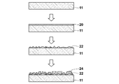
- FIG. 1 shows a process for manufacturing a photoelectric field enhancement substrate according to an embodiment of the photoelectric field enhancement device of the present invention, and is a sectional view for each process.
- a plate-like transparent substrate 11 is prepared, and the transparent substrate 11 is washed with acetone and methanol. Thereafter, as a thin film forming process, aluminum 20 is deposited on the surface of the transparent substrate 11 as a first metal by a thickness of about several tens of nm by sputtering.
- the transparent substrate 11 with the aluminum 20 is immersed in boiling pure water and taken out after a few minutes (about 5 minutes).
- the aluminum 20 becomes transparent and becomes a transparent fine uneven structure layer 22 made of a buyer-mite layer or a boehmite layer constituting the fine uneven structure.
- a second metal is deposited on the fine concavo-convex structure layer 22 as a metal layer manufacturing step.
- the photoelectric field enhancing substrate 1 in which the metal fine uneven structure 24 is generated on the fine uneven structure layer 22 can be produced.
- a plate-like substrate is used as the substrate, but a substrate having an arbitrary shape is applicable.
- the first metal to be hydrothermally reacted in the fine concavo-convex structure layer manufacturing step aluminum is given, but a metal oxide such as alumina (Al (OH) 3 ) may be used instead.
- Aluminum and alumina form a fine concavo-convex structure with a complex triangular pyramid structure consisting of either buyerite (Al [OH] 3 ) or boehmite (AlOOH) or both by hydrothermal reaction on the substrate. (See FIG. 3).
- a metal such as titanium (Ti) that forms a fine uneven structure by a hydrothermal reaction can be used.
- the method for forming the first metal or metal oxide on the substrate 11 is not limited to the sputtering method, and a heating vapor deposition method or a sol-gel method may be used.
- the hydrothermal reaction is not limited to boiling treatment, and the substrate on which the first metal is formed may be exposed to high-temperature water vapor so that the first metal reacts with high-temperature water vapor.
- the second metal constituting the metal fine concavo-convex structure layer 24 may be any metal that can generate localized plasmons when irradiated with excitation light.
- gold Au
- silver Au
- copper Cu
- Aluminum Al
- platinum Pt
- an alloy containing these as a main component Au or Ag is preferable.
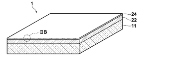
- FIG. 2A is a perspective view of the photoelectric field enhancement substrate 1 obtained by the above manufacturing process
- FIG. 2B is an enlarged view of a part IIB of the side surface of the photoelectric field enhancement substrate 1 shown in FIG. 2A.
- the photoelectric field enhancement substrate 1 includes a substrate 11, a fine concavo-convex structure layer 22 provided on the surface with a fine concavo-convex structure 23, and the fine concavo-convex structure 23.
- the metal fine uneven structure layer (metal layer) 24 formed on the surface of the metal fine uneven structure layer 25 on the surface of the metal fine uneven structure layer 24 is irradiated with light (hereinafter referred to as excitation light). Localized plasmon resonance is induced, and an enhanced photoelectric field is generated on the surface of the metal fine concavo-convex structure layer 24 by the localized plasmon resonance.
- the fine concavo-convex structure layer 22 made of a metal or metal oxide hydroxide such as a buyer-mite layer or a boehmite layer is transparent, and has various sizes (vertical angle sizes) and orientations as shown in FIG. 2B. However, it has a generally serrated cross section. According to the said manufacturing method, the fine concavo-convex structure layer 22 which has the fine concavo-convex structure 23 whose average pitch and depth are generally below the wavelength of excitation light can be obtained.
- the pitch is the distance between the vertices of the nearest adjacent convex portions across the concave portion
- the depth is the distance from the convex portion vertex to the bottom of the adjacent concave portion
- the metal layer 24 regardless of whether the excitation light is incident from the front or back of the substrate.
- a light enhancement field can be generated on the surface, and signal light such as Raman signal light can be detected from either the front or back of the substrate.
- the term “transparent” means that the transmittance is 50% or more with respect to the irradiated light and the light generated from the subject by the light. Note that the transmittance of these lights is preferably 75% or more, and more preferably 90% or more.
- the metal fine concavo-convex structure layer 24 may be formed along the surface of the fine concavo-convex structure layer 22 and may have a fine concavo-convex structure substantially the same as the fine concavo-convex structure 23, but as shown in FIG.
- the fine uneven structure 23 of the fine uneven structure layer 22 may have a fine uneven structure 25 having a different uneven shape on the surface.
- the fine concavo-convex structure layer 22 has substantially the same fine concavo-convex structure as the fine concavo-convex structure layer 23.
- the metal fine concavo-convex structure layer is formed. 2B has a fine concavo-convex structure in which the interval between adjacent convex portions is smaller than the interval between adjacent convex portions of the fine concavo-convex structure 23 corresponding between the adjacent convex portions as shown in FIG. 2B.
- the convex portions 24a are rounded and the distance between adjacent convex portions is smaller than when the metal is simply formed in a film shape along the fine concavo-convex structure 23 of the fine concavo-convex structure layer 22. Yes.
- the interval Wm between the convex portion 25a and the convex portion 25b adjacent to the convex portion 25a It is preferable that there is a portion that is smaller than the interval Wb between the convex portion 23a and the convex portion 23b of the structure 23.
- the interval Wm is half the depth Dm from the apex of the lower convex portion 25b of the adjacent convex portions 25a and 25b to the deepest portion 25c of the concave portion between both convex portions 25a and 25b. This is the distance between the convex portions 25a and 25b at the position of Dm / 2.
- the interval Wb is half the depth Db from the apex of the lower convex portion 23b of the adjacent convex portions 23a and 23b to the deepest portion 23c of the concave portion between both convex portions 23a and 23b. This is the distance between the convex portions 23a and 23b at the position of the depth Db / 2.
- the fine concavo-convex structure 25 of the metal fine concavo-convex structure layer 24 is such that at least one of the length in the direction perpendicular to the substrate and the length in the direction horizontal to the substrate is shorter than the wavelength of the excitation light. Any fine concavo-convex structure may be used as long as it can generate localized plasmons on the surface of the metal fine concavo-convex structure layer 24.
- the convex portions of the fine metal concavo-convex structure layer 24 are in the form of particles formed by aggregation of metals. It is particularly preferable that the granular convex portion has an aspect ratio (length in the direction perpendicular to the substrate / length in the horizontal direction on the substrate) of 0.5 or more. If it is granular, the surface area increases, so the number of analytes attached to the metal surface can be increased, leading to an increase in detection light.
- the average depth from the top of the convex portion of the fine concave-convex structure 25 of the metal fine concave-convex structure layer 24 to the bottom of the adjacent concave portion is 200 nm or less, and the average pitch between the vertices of the nearest convex portions separating the concave portions is 200 nm or less. Preferably there is.
- the metal fine concavo-convex structure layer 24 is formed on the fine concavo-convex structure layer 22 by vapor deposition as in the above-described manufacturing method, when the metal is vapor-deposited on the flat substrate, the thickness is 400 nm or less for gold and 90 nm or less for silver. By depositing with such a deposition amount, it is possible to obtain a metal fine concavo-convex structure that efficiently generates an enhanced photoelectric field.
- the distance between all adjacent convex portions of the fine concavo-convex structure in the formed metal fine concavo-convex structure layer is smaller than the interval between adjacent convex portions of the corresponding fine concavo-convex structure of the substrate.
- the effect of enhancing the photoelectric field becomes more prominent as the number of adjacent convex portions of the metal fine concavo-convex structure layer that is smaller than the interval between adjacent convex portions of the corresponding fine concavo-convex structure of the substrate increases.
- the second metal is only one layer, but two or more kinds of metals may be laminated.
- a dielectric may be laminated on the second metal.
- the film thickness of a dielectric material shall be 50 nm or less.
- 10 nm of SiO 2 is laminated on the metal microstructure layer.
- the fine metal concavo-convex structure layer may be formed by dispersing and disposing fine particles made of the second metal on the surface.
- the fine particles made of the second metal preferably have a diameter of 100 nm or less because a high photoelectric field enhancing effect can be obtained.
- Examples of the method for dispersing and fixing the metal fine particles include the following methods. 1) Metal fine particles are dispersed in an organic solvent, and the colloidal solution is cast on a boehmite substrate and dried. 2) A polycation or a cationic molecular film is adsorbed on a boehmite substrate, and metal fine particles are dispersed and fixed thereon by electrostatic interaction. 3) The boehmite substrate surface is modified with a thiol derivative, and metal fine particles are fixed by utilizing spontaneous bond formation between metal and sulfur. 4) Utilizing the fact that the metal fine particles are negatively charged, the metal fine particles are accumulated on the boehmite substrate by electrophoresis. By the method as described above, a metal fine uneven structure in which metal fine particles are dispersed and fixed on the fine uneven structure layer can be obtained.
- Method for producing photoelectric field enhancement substrate As the substrate 11, a glass substrate (BK-7; Corning Eagle 2000) was used. After ultrasonic cleaning (45 kHz) for 5 minutes with acetone and 5 minutes with methanol, a 25 nm thick aluminum 20 film was formed on the glass substrate 11 using a sputtering apparatus (manufactured by Canon Anelva). In addition, the aluminum thickness was measured using the surface shape measuring device (made by TENCOR), and it confirmed that thickness was 25 nm (+/- 10%).
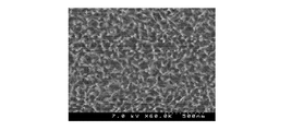
- FIG. 3 The result of having observed the surface of this transparent fine concavo-convex structure layer 22 in SEM (Hitachi S4100) is shown in FIG. In FIG. 3, convex portions are observed in white, and concave portions are observed in gray. Although the uneven pattern is irregular, it is uniformly formed on the entire surface, and the in-plane uniformity of the fine uneven structure is high. From the photograph of the boehmite layer surface shown in FIG. 3, it can be seen that the concavo-convex structure is composed of a number of ridge-shaped convex portions. The uneven structure cross section of the boehmite layer has a sawtooth shape as schematically shown in FIG. 2B.
- a sample in which a metal fine concavo-convex structure layer 24 was formed was formed by depositing Au on the surface of the transparent fine concavo-convex structure layer 22 by EB (Electric Beam) deposition for 30 nm.
- EB Electro Beam
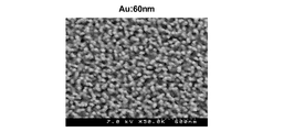
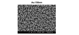
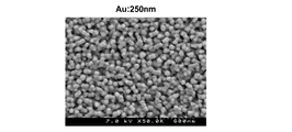
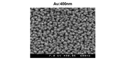
- Au was deposited on the surface of the transparent fine concavo-convex structure layer 22 for 60, 90, 150, 250, and 400 nm, respectively, and Ag was deposited on each of 30, 60, 90, 150, 250, and 400 nm, respectively.
- a sample was made.
- the vapor deposition film thickness here is the same glass substrate as that for the sample, prepared for thickness measurement, part of the surface of the glass substrate for thickness measurement is masked with tape, and the sample substrate is placed in the vapor deposition chamber at the same time. It arrange
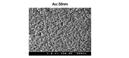
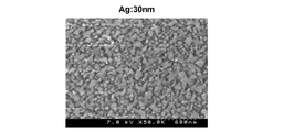
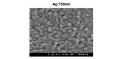
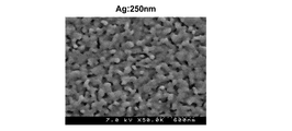
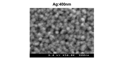
- FIGS. 4A to 4F SEM images of the surface of each sample are shown in FIGS. 4A to 4F for samples prepared by Au deposition, and FIGS. 5A to 5F for samples prepared by Ag deposition.
- the convex portions are aggregated and granulated, and the metal having a granular shape different from the fine uneven structure 25 on the surface of the buyerite or boehmite layer.
- a fine relief structure is formed.
- a metal granular shape is irradiated with light, a very strong photoelectric field called “hot spot” is generated between the particles, which is preferable as a photoelectric field enhancement substrate.
- the granularity increases as the film thickness increases, but the granular shape is maintained even at a film thickness of 400 nm as shown in FIG. 4F.
- the thickness of 150 to 400 nm has a granular structure larger than that of gold.
- Raman scattered light was detected using a microscopic Raman spectroscope (HR800).
- HR800 Raman spectroscope
- laser light having a peak wavelength of 785 nm was used and observed at a magnification of 20 times.
- the laser power immediately after the objective lens was 0.5 mW.
- the irradiation time was 10 seconds.
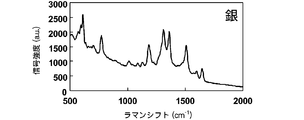
- FIG. 6 and 7 are graphs showing the Raman shift spectrum distribution detected by the microscopic Raman spectroscope, respectively.
- FIG. 6 shows the Raman shift spectrum distribution for a sample in which Au with a film thickness of 60 nm is deposited
- FIG. 7 shows the Raman shift spectrum distribution for a sample in which Ag with a film thickness of 60 nm is deposited.
- a very large Raman signal could be obtained with the sample manufactured using the method for manufacturing a photoelectric field enhancing substrate of the present invention shown in FIGS.
- samples with a thin vapor deposition film thickness (30 nm, 60 nm)
- a larger Raman signal could be obtained when silver was used as the second metal than when gold was used.
- FIG. 8 is a graph in which the peak intensity at 1360 cm ⁇ 1 after white noise removal is plotted with the gold film thickness as the horizontal axis, using the Raman shift spectrum distribution obtained for each sample subjected to Au deposition.
- the signal intensity increases with the film thickness when the gold film thickness is 30 to 90 nm.
- the convex portions of the gold film have a granular structure, and a large number of hot spots are generated by decreasing the distance between the convex portions. It is considered that the signal intensity increases.
- the signal intensity increases when the gold film thickness is 150 to 400 nm.
- the signal intensity is lower than that of the film thickness 30 to 90 nm. This is presumably because the enhancement of the photoelectric field deteriorated due to the increase in particle size or the contact between the particles and conduction.
- the intensity peak is obtained at a film thickness of 90 nm, the photoelectric field enhancement effect can be sufficiently obtained even at a film thickness of 150 to 400 nm, and an enhanced Raman signal is obtained.
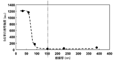
- FIG. 9 is a graph in which the peak intensity at 1360 cm ⁇ 1 after white noise removal is plotted with the silver film thickness as the horizontal axis, using the Raman shift spectrum distribution acquired for each of the samples subjected to Ag vapor deposition.
- the film thickness is 150 nm or more
- the signal intensity sharply decreases and almost no signal is obtained.
- the increase in the size of the photoelectric field deteriorated due to the increase in particle size or the contact and conduction between the particles.
- the silver layer is gradually flattened when the film thickness is thin, and further laminated on the flattened silver layer. it is conceivable that.
Landscapes
- Chemical & Material Sciences (AREA)
- Organic Chemistry (AREA)
- Engineering & Computer Science (AREA)
- Materials Engineering (AREA)
- Chemical Kinetics & Catalysis (AREA)
- Mechanical Engineering (AREA)
- Metallurgy (AREA)
- Inorganic Chemistry (AREA)
- Physics & Mathematics (AREA)
- Health & Medical Sciences (AREA)
- Life Sciences & Earth Sciences (AREA)
- Spectroscopy & Molecular Physics (AREA)
- General Physics & Mathematics (AREA)
- General Chemical & Material Sciences (AREA)
- Geochemistry & Mineralogy (AREA)
- Nuclear Medicine, Radiotherapy & Molecular Imaging (AREA)
- Analytical Chemistry (AREA)
- Biochemistry (AREA)
- General Health & Medical Sciences (AREA)
- Immunology (AREA)
- Pathology (AREA)
- Investigating, Analyzing Materials By Fluorescence Or Luminescence (AREA)
- Investigating Or Analysing Materials By Optical Means (AREA)
- Other Surface Treatments For Metallic Materials (AREA)
Priority Applications (3)
| Application Number | Priority Date | Filing Date | Title |
|---|---|---|---|
| CN201280016792.0A CN103492861B (zh) | 2011-03-31 | 2012-03-26 | 光电场增强器件的制造方法 |
| EP12764916.8A EP2693202B1 (de) | 2011-03-31 | 2012-03-26 | Herstellungsverfahren für eine vorrichtung zur verstärkung eines optisch-elektrischen feldes |
| US14/041,877 US20140034235A1 (en) | 2011-03-31 | 2013-09-30 | Method for producing optical electrical field enhancing device |
Applications Claiming Priority (2)
| Application Number | Priority Date | Filing Date | Title |
|---|---|---|---|
| JP2011077868A JP5801587B2 (ja) | 2011-03-31 | 2011-03-31 | 光電場増強デバイスの製造方法 |
| JP2011-077868 | 2011-03-31 |
Related Child Applications (1)
| Application Number | Title | Priority Date | Filing Date |
|---|---|---|---|
| US14/041,877 Continuation US20140034235A1 (en) | 2011-03-31 | 2013-09-30 | Method for producing optical electrical field enhancing device |
Publications (1)
| Publication Number | Publication Date |
|---|---|
| WO2012132385A1 true WO2012132385A1 (ja) | 2012-10-04 |
Family
ID=46930161
Family Applications (1)
| Application Number | Title | Priority Date | Filing Date |
|---|---|---|---|
| PCT/JP2012/002072 Ceased WO2012132385A1 (ja) | 2011-03-31 | 2012-03-26 | 光電場増強デバイスの製造方法 |
Country Status (5)
| Country | Link |
|---|---|
| US (1) | US20140034235A1 (de) |
| EP (1) | EP2693202B1 (de) |
| JP (1) | JP5801587B2 (de) |
| CN (1) | CN103492861B (de) |
| WO (1) | WO2012132385A1 (de) |
Families Citing this family (9)
| Publication number | Priority date | Publication date | Assignee | Title |
|---|---|---|---|---|
| JP6145861B2 (ja) | 2012-08-15 | 2017-06-14 | 富士フイルム株式会社 | 光電場増強デバイス、光測定装置および方法 |
| JP2014190834A (ja) * | 2013-03-27 | 2014-10-06 | Fujifilm Corp | 光電場増強デバイスおよびその製造方法 |
| JP6229387B2 (ja) * | 2013-09-12 | 2017-11-15 | 大日本印刷株式会社 | 光学部材、及びその製造方法 |
| JP6337127B2 (ja) * | 2014-08-27 | 2018-06-06 | 富士フイルム株式会社 | 光電場増強デバイスおよび光電場増強デバイスの製造方法 |
| CN105158228B (zh) * | 2015-07-30 | 2018-07-20 | 西北大学 | 基于勃姆石纳米薄膜的sers基底及制备方法 |
| EP3350598A4 (de) | 2015-09-17 | 2019-03-27 | Gerhard Maale | Sensorvorrichtung für biosensing und andere anwendungen |
| CN106093007A (zh) * | 2016-06-20 | 2016-11-09 | 上海理工大学 | 一种表面增强拉曼散射基底及其制备方法 |
| CN108275651A (zh) * | 2018-01-22 | 2018-07-13 | 临沂大学 | 一种表面增强拉曼散射基底的制备方法 |
| FR3158725B1 (fr) * | 2024-01-31 | 2026-01-16 | Saint Gobain | Substrat de vitrage |
Citations (11)
| Publication number | Priority date | Publication date | Assignee | Title |
|---|---|---|---|---|
| JPS6148124B2 (de) * | 1977-02-18 | 1986-10-22 | Minnesota Mining & Mfg | |
| JP2005172569A (ja) | 2003-12-10 | 2005-06-30 | Fuji Photo Film Co Ltd | 微細構造体、微細構造体の作製方法、ラマン分光方法および装置 |
| JP2006514286A (ja) | 2003-02-18 | 2006-04-27 | インテル・コーポレーション | 活性表面増強ラマン分光分析(sers)の基体としての金属被覆ナノ結晶シリコン |
| JP2006145230A (ja) | 2004-11-16 | 2006-06-08 | Canon Inc | 被分析物担体およびその製造方法 |
| JP2007240361A (ja) * | 2006-03-09 | 2007-09-20 | Sekisui Chem Co Ltd | 局在プラズモン増強センサ |
| JP2009109395A (ja) * | 2007-10-31 | 2009-05-21 | Fujifilm Corp | 微細構造体の作製方法、微細構造体、ラマン分光用デバイス、ラマン分光装置、分析装置、検出装置、および質量分析装置 |
| JP2009236830A (ja) * | 2008-03-28 | 2009-10-15 | Sumitomo Precision Prod Co Ltd | 被分析物担体、及び、その製造方法 |
| JP4347801B2 (ja) | 2002-06-12 | 2009-10-21 | インテル・コーポレーション | 活性表面増強ラマン分光(sers)基板としての金属被覆ナノ結晶性シリコン |
| JP2012063294A (ja) * | 2010-09-17 | 2012-03-29 | Fujifilm Corp | 光電場増強デバイスを用いた光の測定方法および測定装置 |
| JP2012063293A (ja) * | 2010-09-17 | 2012-03-29 | Fujifilm Corp | 光電場増強デバイス |
| JP2012132743A (ja) * | 2010-12-21 | 2012-07-12 | Fujifilm Corp | 光電場増強デバイスおよび光検出装置 |
Family Cites Families (7)
| Publication number | Priority date | Publication date | Assignee | Title |
|---|---|---|---|---|
| US4252843A (en) * | 1977-02-18 | 1981-02-24 | Minnesota Mining And Manufacturing Company | Process for forming a microstructured transmission and reflectance modifying coating |
| JPH09202649A (ja) * | 1996-01-24 | 1997-08-05 | Central Glass Co Ltd | 花弁状透明アルミナ膜及びその形成法 |
| US6406777B1 (en) * | 2000-06-14 | 2002-06-18 | The United States Of America As Represented By The Secretary Of The Navy | Metal and glass structure for use in surface enhanced Raman spectroscopy and method for fabricating same |
| JP4639241B2 (ja) * | 2007-02-20 | 2011-02-23 | キヤノン株式会社 | 光学用部材、それを用いた光学系及び光学用部材の製造方法 |
| KR20120022754A (ko) * | 2009-03-04 | 2012-03-12 | 유키 하세가와 | 표면 증강 라먼 산란 활성 측정 기판 |
| US8427639B2 (en) * | 2009-05-07 | 2013-04-23 | Nant Holdings Ip, Llc | Surfaced enhanced Raman spectroscopy substrates |
| US20110128535A1 (en) * | 2009-11-30 | 2011-06-02 | David Eugene Baker | Nano-Structured Substrates, Articles, and Methods Thereof |
-
2011
- 2011-03-31 JP JP2011077868A patent/JP5801587B2/ja not_active Expired - Fee Related
-
2012
- 2012-03-26 EP EP12764916.8A patent/EP2693202B1/de not_active Not-in-force
- 2012-03-26 WO PCT/JP2012/002072 patent/WO2012132385A1/ja not_active Ceased
- 2012-03-26 CN CN201280016792.0A patent/CN103492861B/zh not_active Expired - Fee Related
-
2013
- 2013-09-30 US US14/041,877 patent/US20140034235A1/en not_active Abandoned
Patent Citations (11)
| Publication number | Priority date | Publication date | Assignee | Title |
|---|---|---|---|---|
| JPS6148124B2 (de) * | 1977-02-18 | 1986-10-22 | Minnesota Mining & Mfg | |
| JP4347801B2 (ja) | 2002-06-12 | 2009-10-21 | インテル・コーポレーション | 活性表面増強ラマン分光(sers)基板としての金属被覆ナノ結晶性シリコン |
| JP2006514286A (ja) | 2003-02-18 | 2006-04-27 | インテル・コーポレーション | 活性表面増強ラマン分光分析(sers)の基体としての金属被覆ナノ結晶シリコン |
| JP2005172569A (ja) | 2003-12-10 | 2005-06-30 | Fuji Photo Film Co Ltd | 微細構造体、微細構造体の作製方法、ラマン分光方法および装置 |
| JP2006145230A (ja) | 2004-11-16 | 2006-06-08 | Canon Inc | 被分析物担体およびその製造方法 |
| JP2007240361A (ja) * | 2006-03-09 | 2007-09-20 | Sekisui Chem Co Ltd | 局在プラズモン増強センサ |
| JP2009109395A (ja) * | 2007-10-31 | 2009-05-21 | Fujifilm Corp | 微細構造体の作製方法、微細構造体、ラマン分光用デバイス、ラマン分光装置、分析装置、検出装置、および質量分析装置 |
| JP2009236830A (ja) * | 2008-03-28 | 2009-10-15 | Sumitomo Precision Prod Co Ltd | 被分析物担体、及び、その製造方法 |
| JP2012063294A (ja) * | 2010-09-17 | 2012-03-29 | Fujifilm Corp | 光電場増強デバイスを用いた光の測定方法および測定装置 |
| JP2012063293A (ja) * | 2010-09-17 | 2012-03-29 | Fujifilm Corp | 光電場増強デバイス |
| JP2012132743A (ja) * | 2010-12-21 | 2012-07-12 | Fujifilm Corp | 光電場増強デバイスおよび光検出装置 |
Non-Patent Citations (4)
| Title |
|---|
| JUNG-YEN YANG ET AL.: "Detection of Staphylococcus Aureus Using Hydrothermally Roughened Substrates", PROCEEDINGS OF THE 2009 IEEE 3RD INTERNATIONAL CONFERENCE ON NANO/MOLECULAR MEDICINE AND ENGINEERING, 18 October 2009 (2009-10-18), pages 210 - 214, XP031740300 * |
| JUNG-YEN YANG ET AL.: "Surface-Enhanced Raman Scattering Active Substrates", IEEE NANOTECHNOLOGY MAGAZINE, vol. 5, no. 1, 24 February 2011 (2011-02-24), pages 12 - 16, XP011348529 * |
| OPTICS EXPRESS, vol. 17, no. 21, pages 18556 |
| See also references of EP2693202A4 |
Also Published As
| Publication number | Publication date |
|---|---|
| JP2012211839A (ja) | 2012-11-01 |
| US20140034235A1 (en) | 2014-02-06 |
| CN103492861A (zh) | 2014-01-01 |
| JP5801587B2 (ja) | 2015-10-28 |
| EP2693202A4 (de) | 2014-09-03 |
| EP2693202B1 (de) | 2017-11-15 |
| CN103492861B (zh) | 2016-08-10 |
| EP2693202A1 (de) | 2014-02-05 |
Similar Documents
| Publication | Publication Date | Title |
|---|---|---|
| JP5801587B2 (ja) | 光電場増強デバイスの製造方法 | |
| JP5848013B2 (ja) | 光電場増強デバイスおよび該デバイスを備えた測定装置 | |
| US8568878B2 (en) | Directly fabricated nanoparticles for raman scattering | |
| Li et al. | Highly ordered arrays of particle‐in‐bowl plasmonic nanostructures for surface‐enhanced Raman scattering | |
| JP5552007B2 (ja) | 光電場増強デバイス | |
| US8358407B2 (en) | Enhancing signals in Surface Enhanced Raman Spectroscopy (SERS) | |
| CN103109178B (zh) | 利用光电场增强设备的光的测量方法及测量装置 | |
| Gartia et al. | Rigorous surface enhanced Raman spectral characterization of large-area high-uniformity silver-coated tapered silica nanopillar arrays | |
| Sun et al. | A review: nanofabrication of surface-enhanced Raman spectroscopy (SERS) substrates | |
| CN107075661A (zh) | 形成有多个纳米间隙的基底及其制备方法 | |
| Wang et al. | A controlled Ag–Au bimetallic nanoshelled microsphere array and its improved surface-enhanced Raman scattering effect | |
| JP7598614B2 (ja) | ラマン分光測定装置、ラマン分光測定方法および表面増強ラマン散乱デバイス | |
| JP6337127B2 (ja) | 光電場増強デバイスおよび光電場増強デバイスの製造方法 | |
| WO2014156088A1 (ja) | 光電場増強デバイスおよびその製造方法 | |
| JP2014016221A (ja) | 光電場増強デバイスおよびその製造方法 | |
| Ovchinnikov et al. | Self‐Organization‐Based Fabrication of Stable Noble‐Metal Nanostructures on Large‐Area Dielectric Substrates | |
| Kondo et al. | High-Throughput Fabrication of Substrates for Surface-Enhanced Raman Scattering Measurement Based on Nanoimprinting Process Using Anodic Porous Alumina | |
| JP5988239B2 (ja) | 蛍光測定用基板 | |
| Schmidl et al. | Silicon template preparation for the fabrication of thin patterned gold films via template stripping | |
| EP4359772A1 (de) | Sers-substrat mit nanopartikeln | |
| Jing | REALIZATION OF PLASMONIC 2D & 3D NANOSTRUCTURES FOR SURFACE ENHANCED RAMAN SCATTERING DETECTION. |
Legal Events
| Date | Code | Title | Description |
|---|---|---|---|
| 121 | Ep: the epo has been informed by wipo that ep was designated in this application |
Ref document number: 12764916 Country of ref document: EP Kind code of ref document: A1 |
|
| NENP | Non-entry into the national phase |
Ref country code: DE |
|
| REEP | Request for entry into the european phase |
Ref document number: 2012764916 Country of ref document: EP |
|
| WWE | Wipo information: entry into national phase |
Ref document number: 2012764916 Country of ref document: EP |