WO2012141065A1 - 光モジュール及び光モジュールの製造方法 - Google Patents
光モジュール及び光モジュールの製造方法 Download PDFInfo
- Publication number
- WO2012141065A1 WO2012141065A1 PCT/JP2012/059326 JP2012059326W WO2012141065A1 WO 2012141065 A1 WO2012141065 A1 WO 2012141065A1 JP 2012059326 W JP2012059326 W JP 2012059326W WO 2012141065 A1 WO2012141065 A1 WO 2012141065A1
- Authority
- WO
- WIPO (PCT)
- Prior art keywords
- sleeve
- circuit board
- optical element
- optical
- camera
- Prior art date
- Legal status (The legal status is an assumption and is not a legal conclusion. Google has not performed a legal analysis and makes no representation as to the accuracy of the status listed.)
- Ceased
Links
Images










Classifications
-
- G—PHYSICS
- G02—OPTICS
- G02B—OPTICAL ELEMENTS, SYSTEMS OR APPARATUS
- G02B6/00—Light guides; Structural details of arrangements comprising light guides and other optical elements, e.g. couplings
- G02B6/24—Coupling light guides
- G02B6/42—Coupling light guides with opto-electronic elements
- G02B6/4201—Packages, e.g. shape, construction, internal or external details
- G02B6/4219—Mechanical fixtures for holding or positioning the elements relative to each other in the couplings; Alignment methods for the elements, e.g. measuring or observing methods especially used therefor
- G02B6/422—Active alignment, i.e. moving the elements in response to the detected degree of coupling or position of the elements
- G02B6/4221—Active alignment, i.e. moving the elements in response to the detected degree of coupling or position of the elements involving a visual detection of the position of the elements, e.g. by using a microscope or a camera
- G02B6/4224—Active alignment, i.e. moving the elements in response to the detected degree of coupling or position of the elements involving a visual detection of the position of the elements, e.g. by using a microscope or a camera using visual alignment markings, e.g. index methods
-
- G—PHYSICS
- G02—OPTICS
- G02B—OPTICAL ELEMENTS, SYSTEMS OR APPARATUS
- G02B6/00—Light guides; Structural details of arrangements comprising light guides and other optical elements, e.g. couplings
- G02B6/24—Coupling light guides
- G02B6/26—Optical coupling means
- G02B6/32—Optical coupling means having lens focusing means positioned between opposed fibre ends
-
- G—PHYSICS
- G02—OPTICS
- G02B—OPTICAL ELEMENTS, SYSTEMS OR APPARATUS
- G02B6/00—Light guides; Structural details of arrangements comprising light guides and other optical elements, e.g. couplings
- G02B6/24—Coupling light guides
- G02B6/42—Coupling light guides with opto-electronic elements
- G02B6/4201—Packages, e.g. shape, construction, internal or external details
- G02B6/4204—Packages, e.g. shape, construction, internal or external details the coupling comprising intermediate optical elements, e.g. lenses, holograms
- G02B6/4206—Optical features
-
- G—PHYSICS
- G02—OPTICS
- G02B—OPTICAL ELEMENTS, SYSTEMS OR APPARATUS
- G02B6/00—Light guides; Structural details of arrangements comprising light guides and other optical elements, e.g. couplings
- G02B6/24—Coupling light guides
- G02B6/42—Coupling light guides with opto-electronic elements
- G02B6/4201—Packages, e.g. shape, construction, internal or external details
- G02B6/4219—Mechanical fixtures for holding or positioning the elements relative to each other in the couplings; Alignment methods for the elements, e.g. measuring or observing methods especially used therefor
- G02B6/422—Active alignment, i.e. moving the elements in response to the detected degree of coupling or position of the elements
- G02B6/4221—Active alignment, i.e. moving the elements in response to the detected degree of coupling or position of the elements involving a visual detection of the position of the elements, e.g. by using a microscope or a camera
-
- Y—GENERAL TAGGING OF NEW TECHNOLOGICAL DEVELOPMENTS; GENERAL TAGGING OF CROSS-SECTIONAL TECHNOLOGIES SPANNING OVER SEVERAL SECTIONS OF THE IPC; TECHNICAL SUBJECTS COVERED BY FORMER USPC CROSS-REFERENCE ART COLLECTIONS [XRACs] AND DIGESTS
- Y10—TECHNICAL SUBJECTS COVERED BY FORMER USPC
- Y10T—TECHNICAL SUBJECTS COVERED BY FORMER US CLASSIFICATION
- Y10T29/00—Metal working
- Y10T29/49—Method of mechanical manufacture
- Y10T29/49002—Electrical device making
- Y10T29/49117—Conductor or circuit manufacturing
- Y10T29/49124—On flat or curved insulated base, e.g., printed circuit, etc.
Definitions
- the present invention relates to an optical module and a method for manufacturing the optical module.
- an optical module used for optical communication an optical module including a member including a sleeve into which a ferrule fitted to an end of an optical fiber is inserted and an optical element is known.
- alignment of the member provided with the sleeve and the optical element is performed.
- the relative positional accuracy between the optical fiber inserted into the sleeve and the optical element is improved.
- a method described in Patent Document 1 is known.
- the optical element is arranged in a module package part, and a lens is arranged in this module package part.
- the light emitted from the end of the optical fiber is focused on the optical element by the lens, and the light emitted from the optical element is focused on the end of the optical fiber by the lens. Yes.
- the light transmitted through the lens is observed with an observation means (a microscope in the prior art), thereby aligning the member provided with the sleeve with the optical element.
- the present invention has been completed based on the above-described circumstances, and an object thereof is to provide a technique that contributes to improving the positional accuracy between an optical fiber and an optical element.
- the present invention is a method of manufacturing an optical module, comprising: a circuit board on which an optical element is mounted; and a resin member that is disposed on the circuit board and is made of a light-transmitting synthetic resin.
- a resin member that is disposed on the circuit board and is made of a light-transmitting synthetic resin.
- the lens has an optical element active layer that emits or receives invisible light having a single wavelength, and the lens transmits the light when the invisible light transmitted through the lens is inserted into a normal position in the sleeve.
- the optical element active layer is imaged on the optical fiber coupling surface where the end face of the fiber is located, and the resin member and the optical element are irradiated with the invisible light by the camera.
- a relative position between the resin member and the circuit board is observed.
- An alignment step of performing alignment, and a fixing step of fixing the resin member to the circuit board while maintaining a relative position between the resin member and the circuit board in a state where the alignment process is completed To do.
- the camera when the focus of the camera is adjusted to the optical fiber coupling surface, the camera allows the resin member located on the optical fiber coupling surface and the optical element active layer imaged on the optical fiber coupling surface to be simultaneously formed. Can be observed. For this reason, since it is not necessary to move the camera in the middle of the alignment process to change the focus of the camera, it is possible to prevent the camera from being tilted with respect to the axis of the lens in the middle of the alignment process. As a result, it is possible to prevent the positions of the optical element active layer and the resin member from shifting, and thus the alignment accuracy between the optical element active layer and the resin member can be improved.
- the bottom surface of the sleeve is the optical fiber coupling surface, and the bottom surface has an escape hole for allowing the end surface of the optical fiber to escape at a position corresponding to the end surface of the optical fiber when the ferrule is inserted.
- the resin member and the circuit board are relatively aligned by observing a hole edge of the escape hole.
- the edge portion of the relief hole formed on the bottom surface of the sleeve is observed. For this reason, it is not necessary to provide the resin member with a special configuration for performing alignment. As a result, since the structure of the resin member can be simplified, the manufacturing cost can be reduced.
- the wavelength of light used in optical communication and the wavelength of light used in the alignment step are Compared with the case where it differs, the alignment precision can be improved.
- a metal shield member that covers the optical element is insert-molded with the synthetic resin on the resin member, and the shield member protrudes toward the circuit board and has a conductive path formed on the circuit board. It is preferable that a board connecting portion to be connected is formed, and the fixing step is performed by soldering the board connecting portion to the conductive path.
- the resin member and the circuit board can be fixed by a simple method of soldering, the manufacturing cost can be reduced.
- the present invention is also an optical module comprising an optical element mounted on a circuit board, a synthetic resin that is disposed on the circuit board so as to cover the optical element and is light transmissive, and is an optical module. And a sleeve member having a sleeve into which a ferrule fitted on the end of the fiber is inserted. A lens is formed on the sleeve member on the axis of the sleeve, and the optical element is used for optical communication.
- the optical element active layer that emits or receives invisible light having a single wavelength, and the lens has the invisible light transmitted through the lens when the ferrule is inserted at a normal position in the sleeve.
- the optical element active layer is imaged on the optical fiber coupling surface where the end face of the optical fiber is located, and the sleeve member is irradiated with visible light having a wavelength different from that of the invisible light.
- the optical element active layer is imaged on the imaging plane. Further, a mark is formed on the sleeve member at a position corresponding to the imaging plane.
- an observation means such as a camera
- the operator can simultaneously observe the optical element active layer imaged on the imaging surface and the mark formed on the imaging surface. it can.
- the optical element having the optical element active layer and the sleeve member on which the mark is formed can be aligned.
- the step of moving the observation means is not required, it is possible to improve the accuracy of alignment between the optical element and the sleeve member.
- a metal shield member that covers the optical element is insert-molded by the synthetic resin in the sleeve member, and a window portion passes through the shield member on an optical path located between the optical element and the lens.
- the shield member is formed with a board connection portion that protrudes toward the circuit board and is connected to a conductive path formed on the circuit board, and the board connection portion is formed on the circuit board. It is preferable to be soldered to a conductive path formed on the substrate.
- the sleeve member can be disposed on the circuit board by a simple method of soldering.
- an escape hole is formed in the bottom surface of the sleeve to prevent interference with the end face of the optical fiber inserted into the sleeve, and the mark is formed on the inner surface of the escape hole.
- the structure of the sleeve member can be simplified as compared with the case where the mark is formed at a position different from the escape hole.
- a taper surface that decreases in diameter toward the bottom surface of the escape hole is formed at the hole edge of the escape hole, and a boundary portion between the taper surface and the inner wall surface of the escape hole corresponds to the imaging plane. It is preferable that it is formed at a position.
- the boundary between the tapered surface and the inner wall surface of the escape hole can be used as a mark.
- the mark can be formed with a simple configuration in which a tapered surface is formed at the hole edge of the escape hole.
- the bottom surface of the escape hole is formed at a position corresponding to the imaging plane.
- the structure of the sleeve member can be further simplified.
- the sleeve member is formed with a recess depressed on the bottom surface of the sleeve, and the bottom surface of the recess is formed at a position corresponding to the imaging plane.
- the boundary between the bottom surface of the recess and the inner surface of the recess can be used as a mark.
- the positional accuracy between the optical fiber and the optical element can be improved.
- Sectional drawing which shows the optical module which concerns on Embodiment 1 of this invention.
- FIG. Schematic diagram showing the state in which the optical axis of the camera is tilted with respect to the axis of the lens in the prior art
- Sectional drawing which shows the alignment process in the manufacturing method of the optical module which concerns on Embodiment 2.
- FIG. Schematic diagram showing an image displayed on the monitor screen in the present embodiment
- the schematic diagram which shows the state with which the camera and the optical element active layer were aligned
- Sectional drawing which shows the process of fixing a sleeve member and a circuit board in this embodiment.
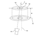
- Sectional drawing which shows the optical module which concerns on Embodiment 3.
- Sectional drawing which shows the optical module which concerns on Embodiment 4.
- an optical module 50 manufactured by the manufacturing method according to the present invention will be described with reference to FIGS. 1 and 2.
- an optical module 50 according to this embodiment includes a circuit board 13 on which an optical element 27 is mounted, and a ferrule 19 that is attached to the plate surface of the circuit board 13 and attached to the end of an optical fiber 18. And a resin member 32 having a sleeve 34 to which is fitted.
- circuit board 13 A conductive path (not shown) is formed on the circuit board 13 by a printed wiring technique.
- the optical element 27 is connected to the conductive path by a known method such as reflow soldering.
- the optical element 27 is at least one of a light receiving element and a light emitting element.
- An optical element active layer 61 is formed on the upper surface of the optical element 27. In the optical element active layer 61, an electric signal is converted into an optical output, or an optical output is converted into an electric signal. In the present embodiment, the optical element active layer 61 has a substantially circular shape with a diameter of about 10 ⁇ m.
- the circuit board 13 is formed with a plurality of through-holes 51 penetrating vertically.
- a conductive path is formed on the inner peripheral surface of the through hole 51.
- a shield member 35 is attached to a surface of the circuit board 13 on which the optical element 27 is mounted so as to cover the optical element 27.
- the shield member 35 is formed by pressing a metal plate material into a predetermined shape.
- the shield member 35 includes a top plate 36 and a side plate 37 extending from the top plate 36 toward the circuit board 13 side.
- a substrate connecting portion 38 extending downward is formed at the lower end edge of the side plate 37.
- the board connecting portion 38 is soldered to the conductive path of the through hole 51 by a known method such as flow soldering while being inserted into the through hole 51 of the circuit board 13.
- the through hole 51 is filled with solder 53 that has solidified after melting.
- the inner diameter of the through hole 51 is set larger than the outer shape of the board connecting portion 38.
- the board connecting portion 38 is movable in a direction parallel to the plate surface of the circuit board 13 in the through hole 51 before being soldered to the through hole 51.
- a resin member 32 is attached to the plate surface of the circuit board 13 on which the optical element 27 is mounted.
- the resin member 32 is made of a light-transmitting synthetic resin (PEI, PC, PMMA, etc.).
- the resin member 32 includes a base portion 33 connected to the circuit board 13 and a sleeve 34 that is formed to extend upward from the base portion 33 and into which the ferrule 19 attached to the end of the optical fiber 18 is inserted.
- the axis 43 of the sleeve 34 is formed substantially perpendicular to the plate surface of the circuit board 13.
- substantially vertical includes the case where the axis line 43 of the sleeve 34 and the plate surface of the circuit board 13 are vertical, and the case where the axis line 43 of the sleeve 34 and the plate surface of the circuit board 13 are not vertical. Including the case of being substantially vertical.
- the base 33 has a substantially rectangular shape when viewed from above.
- the sleeve 34 has a substantially cylindrical shape.
- the bottom surface of the sleeve 34 is an optical fiber coupling surface 60 on which the end surface of the optical fiber 18 is located when the ferrule 19 is inserted at a regular position in the sleeve 34.
- a bottomed hole is formed in the bottom wall of the sleeve 34, and the escape hole 41 is used to prevent interference with the optical fiber 18 inserted into the sleeve 34.
- the cross-sectional shape of the escape hole 41 is substantially circular.
- a lens 39 is formed integrally with the resin member 32 on the optical path located below the sleeve 34 and between the sleeve 34 and the optical element 27.
- the lens 39 is formed to bulge downward toward the circuit board 13.
- light used for optical communication is invisible light having a wavelength of 850 nm.
- the invisible light transmitted through the lens 39 forms an image on the optical element active layer 61 on the optical fiber coupling surface 60 described above.
- a shield member 35 is insert-molded with a synthetic resin at the base 33 of the resin member 32.
- a leg portion 52 extending from the top plate 36 of the shield member 35 protrudes outward from the base portion 33 of the resin member 32.
- the leg 52 is bent at a right angle downward (circuit board 13 side) after insert molding.
- the lower end edge of the leg portion 52 is formed substantially flush with the lower end edge of the resin member 32.
- a window portion 40 penetrating the top plate 36 is formed on an optical path located between the optical element 27 and the lens 39.
- the window 40 secures an optical path between the optical element 27 and the lens 39.
- the gantry 71 is provided with a circuit board moving mechanism 73 for moving the circuit board 13 held by the circuit board holding mechanism 72 in a direction parallel to the plate surface of the circuit board 13.
- the circuit board 13 is held by the circuit board holding mechanism 72 so that the plate surface of the circuit board 13 is horizontal and the optical element 27 faces downward.
- a resin member holding mechanism 74 for holding the resin member 32 is disposed on the gantry 71.
- the resin member 32 is held by the resin member holding mechanism 74 in such a posture that the sleeve 34 is positioned on the lower side and the base portion is positioned on the upper side.
- the resin member 32 is held by the resin member holding mechanism 74 in such a posture that the axis 43 of the sleeve 34 coincides with the vertical direction.
- the pedestal 71 is provided with a camera moving mechanism 82 for moving the camera 76 held by the camera holding mechanism 75 in the vertical direction.
- the camera moving mechanism 82 is also configured to move the camera 76 in the horizontal direction.
- a CCD camera is used as the camera 76.
- any camera can be used as necessary.
- the camera 76 is connected to a monitor 78 via a cable 77. On the monitor 78, an image captured by the camera 76 is displayed.
- a monitor 78 connected to a computer 79 is used as the monitor 78, and the camera 76 and the computer 79 are connected by the cable 77.
- any monitor 78 can be used as necessary as long as the image captured by the camera 76 can be displayed.
- the first aim 80 for aligning the relative positions of the camera 76 and the resin member 32 and the relative positions of the camera 76 and the optical element active layer 61 are displayed on the screen of the monitor 78.
- a second aiming 81 for matching is displayed.
- the first aim 80 and the second aim 81 are formed on a transparent synthetic resin sheet (not shown) by a printing technique, and the sheets are pasted on the screen of the monitor 78.
- the first aim 80 and the second aim 81 may cause the computer 79 to draw the first aim 80 and the second aim 81 and cause the computer 79 to display the image on the screen of the monitor 78. Good.
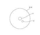
- the first sight 80 is substantially equal to the shape and size of the hole edge 42 displayed on the screen of the monitor 78 when the hole edge 42 of the escape hole 41 formed in the sleeve 34 is imaged by the camera 76. It is formed in shape and size.
- the first aim 80 has a substantially circular shape. Further, the first aim 80 is disposed at a substantially central position in the vertical direction and the horizontal direction on the screen of the monitor 78.
- the second aim 81 is formed in a substantially circular shape having a smaller diameter than the first aim 80.
- the center of the second aim 81 is set concentrically with the center of the first aim 80 having a substantially circular shape on the screen of the monitor 78.
- the second sight 81 is arranged in a region surrounded by the second sight 81 when the optical element active layer 61 imaged by the camera 76 is displayed on the screen of the monitor 78. In this case, the coupling efficiency between the optical fiber 18 and the optical element 27 is set so that a sufficient value can be obtained.
- FIG. 4 shows a state where the circuit board 13, the resin member 32, and the camera 76 are attached to the alignment device 70. 1 and 2, the relative positions of the circuit board 13 and the resin member 32 are reversed in the vertical direction.
- the resin member 32 is held by the resin member holding mechanism 74.
- the board connecting portion 38 of the shield member 35 is inserted into the through hole 51 of the circuit board 13 while moving the circuit board 13 from the upper side to the lower side of the resin member 32.
- the circuit board 13 is held by the circuit board holding mechanism 72.
- the camera 76 is attached to the camera holding mechanism 75. Subsequently, the camera 76 is moved in the vertical direction by the camera moving mechanism 82, and the focus of the camera 76 is adjusted to the optical fiber coupling surface 60 (the bottom surface of the sleeve 34) in a state where white light is irradiated.
- the white light may be an LED light attached to the camera 76, or the resin member 32, the circuit board 13, and the camera 76 may be irradiated with a light that is a separate component from the alignment device 70.
- the lens 39 is set so that the invisible light transmitted through the lens 39 forms an image on the optical element active layer 61 at the optical fiber coupling surface 60. This is expected to improve the coupling efficiency between the optical fiber 18 and the optical element 27.
- the optical path of the invisible light is indicated by a one-dot chain line.
- the white light transmitted through the lens 39 the optical path of the white light is indicated by a broken line in FIG. Since the focal length differs depending on the wavelength, the white light transmitted through the lens 39 forms an image on the optical element active layer 61 at a position inside the escape hole 41. An interval between a position where the optical element active layer 61 is imaged by invisible light and a position where the optical element active layer 61 is imaged by white light is an optical path difference L.
- FIG. 5 shows an example of an image captured by the camera 76.
- a first aim 80 and a second aim 81 are displayed on the screen.
- a hole edge portion 42 of the relief hole 41 formed on the bottom surface of the sleeve 34 is displayed on the screen.
- the white light transmitted through the lens 39 is not displayed on the screen because the optical element active layer 61 does not form an image on the optical fiber coupling surface 60 (the bottom surface of the sleeve 34).
- the inner wall surface and the bottom surface of the sleeve 34 are displayed in the region outside the radial direction of the hole edge 42 of the escape hole 41. However, as described above, since the focus of the camera 76 is adjusted to the optical fiber coupling surface 60, the inner wall surface of the sleeve 34 is displayed as a blurred image that is not in focus. Further, since the resin member 32 is formed of a light-transmitting synthetic resin, the bottom surface of the sleeve 34 is not clearly visible.
- the inner side surface and the bottom surface of the escape hole 41 are displayed in the inner region in the radial direction of the hole edge portion 42 of the escape hole 41. However, since the focal point of the camera 76 is adjusted to the optical fiber coupling surface 60, the inner surface and the bottom surface of the escape hole 41 are displayed as a blurred image that is not in focus.
- the light transmitting synthetic resin constituting the resin member 32 is displayed as a blurred image on the screen of the monitor 78 shown in FIG. Only the hole edge 42 is clearly displayed.
- the camera 76 is moved in the horizontal direction by the camera moving mechanism 82 so that the first aim 80 and the hole edge 42 of the escape hole 41 coincide on the screen of the monitor 78. Let Thereby, the relative alignment of the camera 76 and the resin member 32 is performed.
- the camera moving mechanism 82 moves the camera 76 in the direction (upward) toward the circuit board 13 by the optical path difference L.
- the focal point of the camera 76 is aligned with a virtual surface on which the white light transmitted through the lens 39 forms an image on the optical element active layer 61.
- an image shown in FIG. 8 is displayed.
- a first aim 80, a second aim 81, and an optical element active layer 61 imaged by white light are displayed.
- the hole edge portion 42 of the escape hole 41 is displayed as an unfocused blurred image because the focal point of the camera 76 has moved upward by the optical path difference L. That is, in this state, it cannot be confirmed whether or not the relative positions of the camera 76 and the resin member 32 are aligned.
- the relative position between the camera 76 and the resin member 32 depends on the accuracy of the camera moving mechanism 82.
- the light-transmitting synthetic resin constituting the resin member 32 is displayed on the screen of the monitor 78 as a blurred image that is not in focus.
- the optical element active layer 61 is formed flush with the surface of the optical element 27, the surface of the optical element 27 can also be displayed.
- the optical element active layer 61 is formed so as to protrude or sink into the surface of the optical element 27, the surface of the optical element 27 is also displayed as a blurred image that is not in focus.
- the surface of the circuit board 13 on which the optical element 27 is mounted is also displayed as a blurred image that is not in focus.
- the circuit board 13 is moved by the circuit board moving mechanism 73 so that the optical element active layer 61 is located in the region surrounded by the second aiming 81 on the screen of the monitor 78. Move horizontally. As a result, the relative alignment between the camera 76 and the circuit board 13 is performed.
- the inner diameter of the through hole 51 of the circuit board 13 is set so as not to interfere with the board connecting portion 38 of the shield member 35 when the circuit board 13 is moved in the horizontal direction.
- the relative positions of the resin member 32 and the circuit board 13 are adjusted by aligning the relative positions of the camera 76 and the resin member 32 and then aligning the relative positions of the camera 76 and the circuit board 13. Position can be adjusted.
- the board connection portion 38 of the shield member 35 and the through hole 51 in the circuit board 13 Is soldered by a known method.
- the resin member 32 and the circuit board 13 are fixed in a state where the relative positions of the resin member 32 and the circuit board 13 are matched.
- FIG. 11 illustrates a case where the optical axis of the camera 76 is displaced by an angle ⁇ with respect to the axis 43 of the sleeve 34 when the camera 76 is moved upward.
- the hole edge 42 of the escape hole 41 is not clearly displayed on the screen of the monitor 78 because it is out of focus. For this reason, the operator cannot recognize that the camera 76 is displaced with respect to the axis 43 of the sleeve 34.
- the optical path difference L is shifted in the horizontal direction by the amount multiplied by the value of tan ⁇ .
- the optical path difference L is about 200 ⁇ m.
- the circuit board 13, the resin member 32, and the camera 76 are disposed in the alignment device 70. Subsequently, the camera 76 is moved in the vertical direction by the camera moving mechanism 82, and invisible light having a wavelength of 850 nm is irradiated by a light source (not shown), the camera 76 is focused on the optical fiber coupling surface 60 (the bottom surface of the sleeve 34). Adjust to.
- the optical path of invisible light is indicated by a one-dot chain line in FIG.
- an image as shown in FIG. 13 is displayed on the screen of the monitor 78, for example.
- the active surface of the optical element 27 formed on the optical fiber coupling surface 60 by invisible light transmitted through the first aim 80, the second aim 81, the hole edge 42 of the escape hole 41, and the lens 39. is displayed. That is, in the present embodiment, the first aim 80 and the second aim 81 that are the reference for alignment, the hole edge 42 of the escape hole 41 formed in the resin member 32 that is the object of alignment, and the alignment
- the optical element active layer 61 which is the target of the above, is clearly displayed on the same screen.
- the camera 76 is moved in the horizontal direction by the camera moving mechanism 82 so that the first aim 80 and the hole edge 42 of the escape hole 41 coincide with each other. Thereby, the relative alignment of the camera 76 and the resin member 32 is performed.
- the circuit board 13 is moved in the horizontal direction by the circuit board moving mechanism 73 so that the optical element active layer 61 is located in the region surrounded by the second aiming 81. Thereby, relative alignment of the camera 76 and the optical element active layer 61 is performed. Thereby, the relative alignment of the camera 76, the resin member 32, and the optical element active layer 61 is completed.
- the camera 76 since it is not necessary to move the camera 76, it is possible to prevent the camera 76 from being tilted with respect to the axis of the lens 39 during the alignment process. As a result, it is possible to prevent the positions of the optical element active layer 61 and the resin member 32 from being shifted, so that the alignment accuracy between the optical element active layer 61 and the resin member 32 can be improved.
- the hole edge portion 42 of the escape hole 41 formed on the bottom surface of the sleeve 34 is observed in the alignment step. For this reason, it is not necessary to provide the resin member 32 with a special configuration for alignment. As a result, since the structure of the resin member 32 can be simplified, the manufacturing cost can be reduced.
- invisible light having the same wavelength as invisible light used in optical communication is used in the alignment process, so the wavelength of light used in optical communication and the wavelength of light used in the alignment process As compared with the case where the difference is different from the above, the alignment accuracy can be improved.
- the resin member 32 and the circuit board can be formed by a simple method of soldering to the board connection portion 38 of the shield member 35 insert-molded in the resin member 32 and the through hole 51 of the circuit board 13. 13 can be fixed, so that the manufacturing cost can be reduced.
- the optical module 150 includes an optical element 127 mounted on the circuit board 113, and a ferrule 119 attached to the plate surface of the circuit board 113 and attached to the end of the optical fiber 118. And a sleeve member 132 having a sleeve 134 to which is fitted.
- circuit board 113 A conductive path (not shown) is formed on the circuit board 113 by a printed wiring technique.
- the optical element 127 is connected to the conductive path by a known method such as reflow soldering.
- the optical element 127 is at least one of a light receiving element and a light emitting element.
- An optical element active layer 161 is formed on the upper surface of the optical element 127. In the optical element active layer 161, an electric signal is converted into an optical output, or an optical output is converted into an electric signal.
- the optical element active layer 161 has a substantially circular shape with a diameter of about 10 ⁇ m.
- the circuit board 113 has a plurality of through-holes 151 penetrating vertically.
- a conductive path is formed on the inner peripheral surface of the through hole 151.
- a shield member 135 is attached to a surface of the circuit board 113 on which the optical element 127 is mounted so as to cover the optical element 127.
- the shield member 135 is formed by pressing a metal plate into a predetermined shape.
- the shield member 135 includes a top plate 136 and a side plate 137 extending from the top plate 136 toward the circuit board 113 side.
- a board connecting portion 138 extending downward is formed at the lower edge of the side plate 137.
- the board connection portion 138 is soldered to the conductive path of the through hole 151 by a known method such as flow soldering while being inserted into the through hole 151 of the circuit board 113.
- the through-hole 151 is filled with solder 153 that is solidified after melting.
- the inner diameter of the through hole 151 is set to be larger than the outer shape of the board connecting portion 138. Accordingly, the board connecting portion 138 is movable in a direction parallel to the plate surface of the circuit board 113 in the through hole 151 before being soldered to the through hole 151.
- a sleeve member 132 is attached to a surface of the circuit board 113 on which the optical element 127 is mounted so as to cover the optical element 127.
- the sleeve member 132 is made of a light-transmitting synthetic resin (PEI, PC, PMMA, etc.).
- the sleeve member 132 includes a base portion 133 connected to the circuit board 113 and a sleeve 134 that is formed to extend upward from the base portion 133 and into which a ferrule 119 attached to the end of the optical fiber 118 is inserted.
- An axis 143 of the sleeve 134 is formed substantially perpendicular to the plate surface of the circuit board 113.
- substantially vertical includes the case where the axis 143 of the sleeve 134 and the plate surface of the circuit board 113 are vertical, and the axis 143 of the sleeve 134 and the board surface of the circuit board 113 are not vertical. Including the case of being substantially vertical.
- the base 133 has a substantially rectangular shape when viewed from above.
- the sleeve 134 has a substantially cylindrical shape.
- the bottom surface of the sleeve 134 is an optical fiber coupling surface 160 on which the end surface of the optical fiber 118 is positioned when the ferrule 119 is inserted at a normal position in the sleeve 134.
- a bottomed hole is formed in the bottom wall of the sleeve 134 so as to be an escape hole 141 for preventing interference with the optical fiber 118 inserted into the sleeve 134.
- the cross-sectional shape of the escape hole 141 is substantially circular.
- the sleeve member 132 has a lens 139 formed integrally with the sleeve member 132 on the optical path located below the sleeve 134 and between the sleeve 134 and the optical element 127.
- the lens 139 is formed to bulge downward toward the circuit board 113. With this lens 139, the light output emitted from the optical fiber 118 is condensed on the optical element 127, and the light output emitted from the optical element 127 is condensed on the lower end surface of the optical fiber 118. It has come to be.
- light used for optical communication is invisible light having a wavelength of 850 nm.
- the invisible light transmitted through the lens 139 forms an image on the optical element active layer 161 on the optical fiber coupling surface 160 described above.
- the shield member 135 is insert-molded with a synthetic resin at the base 133 of the sleeve member 132. From the base portion 133 of the sleeve member 132, leg portions 152 extending from the top plate 136 of the shield member 135 protrude outward. The leg 152 is bent at a right angle downward (circuit board 113 side) after insert molding. The lower end edge of the leg portion 152 is formed substantially flush with the lower end edge of the sleeve member 132.
- a window portion 140 penetrating the top plate 136 is formed on the optical path located between the optical element 127 and the lens 139.
- the window 140 secures an optical path between the optical element 127 and the lens 139.
- the hole edge 142 of the escape hole 141 is formed with a tapered surface 145 in which the inner diameter of the escape hole 141 is reduced from the hole edge 142 toward the bottom surface of the escape hole 141.
- the boundary between the tapered surface 145 and the inner surface of the escape hole 141 is a boundary portion 146. This boundary portion 146 is an example of a mark.
- the light is refracted by passing through the lens 139. Since the refractive index of light varies depending on the wavelength, for example, the refractive index differs between invisible light having a wavelength of 850 nm and white light. As a result, for the invisible light having a wavelength of 850 nm transmitted through the lens 139, the optical element active layer 161 is imaged on the optical fiber coupling surface 160 described above, whereas for the white light transmitted through the lens 139, optical fiber coupling is performed. The optical element active layer 161 is imaged at a position closer to the optical element 127 than the surface 160. In the present embodiment, the optical element active layer 161 is imaged at a position inside the escape hole 141. In FIG.
- the optical path of invisible light having a wavelength of 850 nm is indicated by a one-dot chain line, and the optical path of white light is indicated by a broken line.
- the distance between the optical fiber coupling surface 160 and the imaging surface 144 is an optical path difference M.
- a virtual surface on which white light transmitted through the lens 139 forms an image on the optical element active layer 161 is defined as an image forming surface 144.
- the boundary portion 146 described above is formed at a position corresponding to the imaging plane 144.
- the white light according to the present embodiment is at least visible light different from the wavelength of invisible light used for optical communication.
- the gantry 171 is provided with a circuit board moving mechanism 173 that moves the circuit board 113 held by the circuit board holding mechanism 172 in a direction parallel to the plate surface of the circuit board 113.
- the circuit board 113 is held by the circuit board holding mechanism 172 so that the plate surface of the circuit board 113 is horizontal and the optical element 127 faces downward.
- a sleeve member holding mechanism 174 for holding the sleeve member 132 is disposed on the gantry 171.
- the sleeve member 132 is held by the sleeve member holding mechanism 174 in such a posture that the sleeve 134 is positioned on the lower side and the base portion is positioned on the upper side.
- the sleeve member 132 is held by the sleeve member holding mechanism 174 in such a posture that the axis 143 of the sleeve 134 coincides with the vertical direction.
- a camera moving mechanism 182 for moving the camera 176 held by the camera holding mechanism 175 in the vertical direction is disposed on the gantry 171.
- the camera moving mechanism 182 also moves the camera 176 in the horizontal direction.
- a CCD camera is used as the camera 176.
- any camera can be used as necessary.
- the camera 176 is connected to the monitor 178 via the cable 177. On the monitor 178, an image captured by the camera 176 is displayed.
- a monitor 178 connected to a computer 179 is used as the monitor 178, and the camera 176 and the computer 179 are connected by the cable 177.
- any monitor 178 can be used as necessary as long as it can display an image captured by the camera 176.
- the first aim 180 for aligning the relative positions of the camera 176 and the sleeve member 132 and the relative positions of the camera 176 and the optical element active layer 161 are displayed on the screen of the monitor 178.
- a second aim 181 for matching is displayed.
- the first aim 180 and the second aim 181 are formed on a transparent synthetic resin sheet (not shown) by a printing technique, and the sheets are pasted on the screen of the monitor 178.
- the first aim 180 and the second aim 181 may cause the computer 179 to draw the first aim 180 and the second aim 181, and the computer 179 may display the image on the screen of the monitor 178. Good.
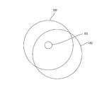
- the first aim 180 is substantially equal to the shape and size of the hole edge 142 displayed on the screen of the monitor 178 when the hole edge 142 of the escape hole 141 formed in the sleeve 134 is imaged by the camera 176. It is formed in shape and size. In the present embodiment, the first aim 180 has a substantially circular shape. In addition, the first aim 180 is disposed at a substantially central position in the vertical direction and the horizontal direction on the screen of the monitor 178.
- the second aim 181 is formed in a substantially circular shape having a smaller diameter than the first aim 180.
- the center of the second aim 181 is set concentrically with the center of the first aim 180 having a substantially circular shape on the screen of the monitor 178.
- the second sight 181 is arranged in a region surrounded by the second sight 181 in a state in which the optic active layer 161 imaged by the camera 176 is displayed on the screen of the monitor 178. In such a case, the coupling efficiency between the optical fiber 118 and the optical element 127 is set so that a sufficient value can be obtained.
- FIG. 20 shows a state where the circuit board 113, the sleeve member 132, and the camera 176 are attached to the alignment device 170. 17 and 18, the relative positions of the circuit board 113 and the sleeve member 132 are reversed in the vertical direction.
- the difference between the optical module 150 according to the conventional technique and the optical module 150 according to the second embodiment is that the boundary portion 246 is not formed at a position corresponding to the imaging plane 144 in the sleeve member 132.
- the boundary portion 246 is formed at a position closer to the bottom surface of the sleeve 134 than the image plane 144.
- the sleeve member 132 is held by the sleeve member holding mechanism 174.
- the board connecting portion 138 of the shield member 135 is inserted into the through hole 151 of the circuit board 113 while moving the circuit board 113 from the upper side to the lower side of the sleeve member 132.
- the circuit board 113 is held by the circuit board holding mechanism 172.
- the camera 176 is attached to the camera holding mechanism 175. Subsequently, the camera 176 is moved up and down by the camera moving mechanism 182, and the focus of the camera 176 is adjusted to the optical fiber coupling surface 160 (the bottom surface of the sleeve 134) in a state where white light is irradiated.
- the white light may be an LED light attached to the camera 176, or the sleeve member 132, the circuit board 113, and the camera 176 may be irradiated with a light that is a separate component from the alignment device 170.
- the optical module 150 As described above, in the optical module 150 according to the present embodiment, invisible light having a wavelength of 850 nm is used for optical communication. Therefore, the invisible light transmitted through the lens 139 forms an image on the optical element active layer 161 at the optical fiber coupling surface 160. This is expected to improve the coupling efficiency between the optical fiber 118 and the optical element 127.
- the optical path of the invisible light is indicated by a one-dot chain line.
- the white light transmitted through the lens 139 has a white light path indicated by a broken line. Since the focal length varies depending on the wavelength, the white light transmitted through the lens 139 forms an image on the optical element active layer 161 at a position inside the escape hole 141.
- FIG. 21 shows an example of an image captured by the camera 176.
- a first aim 180 and a second aim 181 are displayed on the screen.
- a hole edge 142 of the escape hole 141 formed on the bottom surface of the sleeve 134 is displayed on the screen.
- the white light transmitted through the lens 139 is not displayed on the screen because the optical element active layer 161 does not form an image on the optical fiber coupling surface 160 (the bottom surface of the sleeve 134).
- the inner wall surface and the bottom surface of the sleeve 134 are displayed in the outer region in the radial direction of the hole edge 142 of the escape hole 141. However, as described above, since the focus of the camera 176 is adjusted to the optical fiber coupling surface 160, the inner wall surface of the sleeve 134 is displayed as a blurred image that is not in focus. Further, since the sleeve member 132 is formed of a light-transmitting synthetic resin, the bottom surface of the sleeve 134 is not clearly visible.
- the inner side surface and the bottom surface of the escape hole 141 are displayed in the inner region in the radial direction of the hole edge 142 of the escape hole 141. However, since the focus of the camera 176 is adjusted to the optical fiber coupling surface 160, the inner surface and the bottom surface of the escape hole 141 are displayed as a blurred image that is not in focus.
- the light-transmitting synthetic resin constituting the sleeve member 132 is displayed as a blurred image on the screen of the monitor 178 shown in FIG. Only the hole edge 142 is clearly displayed.
- the camera 176 is moved in the horizontal direction by the camera moving mechanism 182 so that the first aim 180 and the hole edge 142 of the escape hole 141 coincide on the screen of the monitor 178. Let Thereby, relative alignment of the camera 176 and the sleeve member 132 is performed.
- the camera moving mechanism 182 moves the camera 176 toward the circuit board 113 by the optical path difference M (upward).
- the focus of the camera 176 is aligned with a virtual surface on which the white light transmitted through the lens 139 forms an image on the optical element active layer 161.
- an image shown in FIG. 24 is displayed on the screen of the monitor 178.
- a first aim 180, a second aim 181, and an optical element active layer 161 imaged by white light are displayed on the screen of the monitor 178.
- the hole edge 142 of the escape hole 141 is displayed as an unfocused blurred image because the focus of the camera 176 has moved upward by the optical path difference M. That is, in this state, it cannot be confirmed whether or not the relative positions of the camera 176 and the sleeve member 132 are aligned.
- the relative position of the camera 176 and the sleeve member 132 can only depend on the accuracy of the camera moving mechanism 182.
- the light transmissive synthetic resin constituting the sleeve member 132 is displayed as a blurred image that is not in focus.
- the surface of the optical element 127 can also be displayed.
- the optical element active layer 161 is formed so as to protrude or dip into the surface of the optical element 127
- the surface of the optical element 127 is also displayed as a blurred image that is out of focus.
- the surface of the circuit board 113 on which the optical element 127 is mounted is also displayed as a blurred image that is not in focus.
- the focus of the camera 176 is moved upward by the optical path difference M
- the light-transmitting synthetic resin constituting the sleeve member 132, the optical element 127, and the like are displayed on the screen of the monitor 178.
- the circuit board 113 is displayed as an out-of-focus blurred image, and only the optical element active layer 161 is clearly displayed.
- the circuit board 113 is moved by the circuit board moving mechanism 173 so that the optical element active layer 161 is located in the region surrounded by the second aim 181. Move horizontally. Thereby, relative alignment between the camera 176 and the circuit board 113 is performed.
- the inner diameter of the through hole 151 of the circuit board 113 is set so as not to interfere with the board connection portion 138 of the shield member 135 when the circuit board 113 is moved in the horizontal direction.
- the relative positions of the sleeve member 132 and the circuit board 113 are adjusted by aligning the relative positions of the camera 176 and the sleeve member 132 and then aligning the relative positions of the camera 176 and the circuit board 113. Position can be adjusted.
- FIG. 26 With the relative positions of the camera 176, the sleeve member 132, and the circuit board 113 held, the board connecting portion 138 of the shield member 135 and the through hole 151 to the circuit board 113 Is soldered by a known method.
- the sleeve member 132 and the circuit board 113 are fixed in a state where the relative positions of the sleeve member 132 and the circuit board 113 are matched.
- FIG. 27 illustrates a case where the optical axis of the camera 176 is shifted by the angle ⁇ with respect to the axis 143 of the sleeve 134 when the camera 176 is moved upward.
- the hole edge 142 of the escape hole 141 is not clearly displayed on the screen of the monitor 178 because it is out of focus. For this reason, the operator cannot recognize that the camera 176 has shifted with respect to the axis 143 of the sleeve 134.
- the optical path difference M is shifted in the horizontal direction by the amount obtained by multiplying the value of tan ⁇ .
- the optical path difference M is about 200 ⁇ m.
- the circuit board 113, the sleeve member 132, and the camera 176 are disposed in the alignment device 170. Subsequently, the camera 176 is moved up and down by the camera moving mechanism 182, and the focus of the camera 176 is adjusted to the imaging plane 144 in a state where white light is irradiated by a light source (not shown). The optical path of white light is indicated by a broken line in FIG.
- an image as shown in FIG. 29 is displayed on the screen of the monitor 178, for example.
- the optical element active layer 161 imaged on the imaging surface 144 by the white light transmitted through the first aim 180, the second aim 181, the boundary 146, and the lens 139 is displayed.
- the element active layer 161 is clearly displayed on the same screen.
- the camera 176 is moved in the horizontal direction by the camera moving mechanism 182, and the first aim 180 and the boundary portion 146 are made to coincide with each other. Thereby, relative alignment of the camera 176 and the sleeve member 132 is performed.
- the circuit board 113 is moved in the horizontal direction by the circuit board moving mechanism 173 so that the optical element active layer 161 is located in the region surrounded by the second aim 181.
- the circuit board moving mechanism 173 moves the optical element active layer 161 in the region surrounded by the second aim 181.
- relative alignment of the camera 176 and the optical element active layer 161 is performed.
- the relative alignment of the camera 176, the sleeve member 132, and the optical element active layer 161 is completed.
- the through-holes between the board connecting portion 138 of the shield member 135 and the circuit board 113 while maintaining the relative positions of the camera 176, the sleeve member 132, and the optical element active layer 161. 151 is soldered by a known method. Accordingly, in the present embodiment, the sleeve member 132 and the circuit board 113 are fixed in a state where the relative positions of the sleeve member 132 and the circuit board 113 are matched.
- the camera 176 since it is not necessary to move the camera 176, the camera 176 is prevented from being tilted with respect to the axis of the lens 139 during the alignment process. As a result, it is possible to prevent the optical element active layer 161 and the sleeve member 132 from being displaced from each other, so that the alignment accuracy between the optical element active layer 161 and the sleeve member 132 can be improved.
- the boundary portion 146 formed inside the escape hole 141 is observed in the alignment step. For this reason, it is not necessary to provide the sleeve member 132 with a special configuration for performing alignment. As a result, the structure of the sleeve member 132 can be simplified, and the manufacturing cost can be reduced.
- a boundary portion 146 between the tapered surface 145 formed on the hole edge 142 of the escape hole 141 and the inner side surface of the escape hole 141 can be used as a mark.
- a mark for executing alignment between the sleeve member 132 and the optical element 127 can be formed with a simple configuration in which the tapered surface 145 is formed.
- the sleeve member 132 and the circuit board are soldered to each other by a simple method of soldering to the board connecting portion 138 of the shield member 135 insert-molded in the sleeve member 132 and the through hole 151 of the circuit board 113. 113 can be fixed, so that the manufacturing cost can be reduced.
- the bottom surface of the escape hole 141 formed in the sleeve member 132 is formed at a position corresponding to the imaging surface 144.
- the boundary between the bottom surface of the escape hole 141 and the inner side surface of the escape hole 141 is an example of the mark 191.
- the boundary portion 346 is not formed at a position corresponding to the imaging plane 144. Specifically, the boundary portion 346 is formed at a position closer to the bottom surface of the sleeve 134 than the image plane 144 (upward in FIG. 33). Since the configuration other than the above is substantially the same as that of the second embodiment, the same members are denoted by the same reference numerals, and redundant description is omitted.
- the boundary between the bottom surface of the escape hole 141 and the inner side surface of the escape hole 141 can be the mark 191.
- the operator can perform alignment between the camera 176 and the sleeve member 132 by aligning the mark 191 relative to the first aim 180.
- the mark 191 can be formed with a simple configuration in which the position of the bottom surface of the escape hole 141 corresponds to the imaging surface 144, so that the structure of the sleeve member 132 can be further simplified.
- a concave portion 193 is recessed and formed on the bottom surface of the sleeve 134 at a position different from the escape hole 141.
- the bottom surface of the recess 193 is formed at a position corresponding to the image plane 144.
- the boundary between the bottom surface of the recess 193 and the inner surface of the recess 193 is an example of the mark 194.
- the boundary portion 346 is not formed at a position corresponding to the imaging plane 144. Specifically, the boundary portion 346 is formed at a position closer to the bottom surface of the sleeve 134 than the image plane 144 (upward in FIG. 34). Since the configuration other than the above is substantially the same as that of the second embodiment, the same members are denoted by the same reference numerals, and redundant description is omitted.
- the boundary between the bottom surface of the recess 193 and the inner surface of the recess 193 can be used as the mark 194. Accordingly, the operator can perform alignment between the camera 176 and the sleeve member 132 by aligning the mark 194 relative to the first aim 180.
- the recess 193 is formed at a position different from the escape hole 141. For this reason, it is necessary to form the escape hole 141 at a position corresponding to the end face of the optical fiber 118, whereas the recess 193 can be formed at a relatively free position. As a result, by forming the recess 193 at a position that is easy for the operator to visually recognize, the alignment operation between the optical element 127 and the sleeve member 132 can be easily performed.
- the present invention is not limited to the embodiments described with reference to the above description and drawings.
- the following embodiments are also included in the technical scope of the present invention.
- the present invention is not limited to this, and the resin member 32 requires a rib or a recess at a position corresponding to the optical fiber coupling surface 60. Accordingly, an arbitrary structure may be formed, and the above structure may be observed in the alignment step.
- invisible light having a wavelength of 850 nm is used.
- the invisible light is not limited to this, and any invisible light used for optical communication may be used as required, such as 1.3 ⁇ m and 1.55 ⁇ m.
- the resin member 32 and the circuit board 13 are fixed by soldering.
- the present invention is not limited to this, and the resin member 32 and the circuit board 13 may be bonded with an adhesive.
- the resin member 32 and the circuit board 13 may be screwed together, and the resin member 32 and the circuit board 13 can be fixed by any method as necessary.
- the mark is defined as the boundary portion 146, the boundary between the bottom surface of the escape hole 141 and the inner surface of the escape hole 141, and the boundary between the bottom surface of the recess and the inner surface of the recess.
- the present invention is not limited to this, and the sleeve member 132 is formed with an arbitrary structure as necessary, such as a rib or a convex portion, at a position corresponding to the imaging surface 144, and the above structure is observed in the alignment step. May be.
- the alignment process is performed using white light.
- the present invention is not limited to this, and monochromatic light or the like may be used as long as it is visible light having a wavelength different from that of invisible light used for optical communication. If necessary, visible light having any wavelength can be used.
- the sleeve member 132 and the circuit board 113 are fixed by soldering. However, the present invention is not limited to this, and the sleeve member 132 and the circuit board 113 are bonded with an adhesive. Alternatively, the sleeve member 132 and the circuit board 113 may be screwed together, and the sleeve member 132 and the circuit board 113 can be fixed by any method as necessary.
- the shield member 135 is insert-molded with a synthetic resin.
- the present invention is not limited to this, and the shield member 135 is formed separately from the sleeve member 132, so that the circuit board 113 is formed. It is good also as a structure fixed separately with respect to.
Landscapes
- Physics & Mathematics (AREA)
- General Physics & Mathematics (AREA)
- Optics & Photonics (AREA)
- Optical Couplings Of Light Guides (AREA)
Abstract
Description
前記スリーブの底面は前記光ファイバ結合面とされており、前記底面には前記フェルールが挿入されたときに前記光ファイバの端面に対応する位置に、前記光ファイバの端面を逃がすための逃がし孔が陥没して形成されており、前記位置合わせ工程においては、前記逃がし孔の孔縁部を観察することにより前記樹脂部材と、前記回路基板と、の相対的な位置合わせを行うことが好ましい。
前記スリーブ部材には前記光素子を覆う金属製のシールド部材が前記合成樹脂によってインサート成型されており、前記シールド部材には前記光素子と前記レンズとの間に位置する光路上に窓部が貫通して形成されており、前記シールド部材には前記回路基板に向けて突出すると共に前記回路基板に形成された導電路に接続される基板接続部が形成されており、前記基板接続部は前記回路基板に形成された導電路にはんだ付けされていることが好ましい。
1. 光モジュール50
まず、本発明に係る製造方法によって製造された光モジュール50について、図1及び図2を参照しつつ説明する。図1に示すように、本実施形態に係る光モジュール50は、光素子27が実装された回路基板13と、回路基板13の板面に取り付けられると共に光ファイバ18の端末に装着されたフェルール19が嵌合されるスリーブ34を備えた樹脂部材32と、を備える。
回路基板13にはプリント配線技術により図示しない導電路が形成されている。回路基板13の上面には、光素子27が導電路とリフローはんだ付け等の公知の手法により接続されている。光素子27は、受光素子及び発光素子の少なくとも一方である。光素子27の上面には、光素子活性層61が形成されている。この光素子活性層61において、電気信号が光出力に変換され、又は、光出力が電気信号に変換される。本実施形態においては、光素子活性層61は、直径約10μmの略円形状をなしている
回路基板13の板面のうち、光素子27が実装された板面には、光素子27を覆うようにしてシールド部材35が取り付けられている。シールド部材35は金属板材を所定の形状にプレス加工してなる。シールド部材35は、天板36と、この天板36から回路基板13側に向けて延びる側板37と、を備える。側板37の下端縁には、下方に延びる基板接続部38が形成されている。この基板接続部38が、回路基板13のスルーホール51内に挿入された状態で、フローはんだ付け等の公知の手法により、スルーホール51の導電路とはんだ付けされている。スルーホール51内には、溶融後に固化したはんだ53が充填されている。
回路基板13の板面のうち、光素子27が実装された板面には、樹脂部材32が取り付けられている。樹脂部材32は光透過性の合成樹脂(PEI,PC,PMMA等)からなる。樹脂部材32は、回路基板13に接続される基部33と、基部33から上方に延びて形成されると共に光ファイバ18の端末に装着されたフェルール19が挿入されるスリーブ34と、を備える。スリーブ34の軸線43は、回路基板13の板面と実質的に垂直に形成されている。なお、実質的に垂直とは、スリーブ34の軸線43と回路基板13の板面とが垂直である場合を含み、且つ、スリーブ34の軸線43と回路基板13の板面とが垂直でない場合でも、実質的に垂直である場合も含む。
続いて、本発明に係る製造方法に用いられる調芯装置70について、図3を参照しつつ説明する。架台71には、回路基板保持機構72に保持された回路基板13を、回路基板13の板面に平行な方向に移動させる回路基板移動機構73が配設されている。回路基板13は、回路基板13の板面が水平になる姿勢で、且つ、光素子27が下方を向く姿勢で回路基板保持機構72に保持される。
続いて、従来技術に係る調芯方法について、図4ないし図9を参照しつつ説明する。図4には、回路基板13、樹脂部材32、及びカメラ76が、調芯装置70に取り付けられた状態を示す。図1及び図2とは、回路基板13及び樹脂部材32の相対的な位置が上下方向について逆になっている。
続いて、従来技術の問題点について説明する。まず、従来技術においては、図6に示すように、カメラ76と樹脂部材32との相対的な位置合わせを行った後、図7に示すように、カメラ76を光路差Lの分だけ上方に移動させる。このため、作業工程が煩雑になるという問題がある。
続いて、本願発明を光素子27の製造方法に適用した一実施形態について、図12ないし図15を参照しつつ説明する。また、上記した従来技術と同一構成、及び同一工程については、重複する説明を省略する。
続いて、本実施形態の作用、効果について説明する。本実施形態によれば、カメラ76の焦点を光ファイバ結合面60に調節すると、このカメラ76によって、この光ファイバ結合面60に位置する樹脂部材32と、光ファイバ結合面60に結像する光素子活性層61と、を同時に観察することができる。このため、位置合わせ工程の途中でカメラ76の焦点を変更する必要がないので、作業工数を減少させることができる。
1. 光モジュール150
まず、本発明の実施形態2に係る光モジュール150について、図17及び図18を参照しつつ説明する。図17に示すように、本実施形態に係る光モジュール150は、回路基板113に実装された光素子127と、回路基板113の板面に取り付けられると共に光ファイバ118の端末に装着されたフェルール119が嵌合されるスリーブ134を備えたスリーブ部材132と、を備える。
回路基板113にはプリント配線技術により図示しない導電路が形成されている。回路基板113の上面には、光素子127が導電路とリフローはんだ付け等の公知の手法により接続されている。光素子127は、受光素子及び発光素子の少なくとも一方である。光素子127の上面には、光素子活性層161が形成されている。この光素子活性層161において、電気信号が光出力に変換され、又は、光出力が電気信号に変換される。本実施形態においては、光素子活性層161は、直径約10μmの略円形状をなしている
回路基板113の板面のうち、光素子127が実装された板面には、光素子127を覆うようにしてシールド部材135が取り付けられている。シールド部材135は金属板材を所定の形状にプレス加工してなる。シールド部材135は、天板136と、この天板136から回路基板113側に向けて延びる側板137と、を備える。側板137の下端縁には、下方に延びる基板接続部138が形成されている。この基板接続部138が、回路基板113のスルーホール151内に挿入された状態で、フローはんだ付け等の公知の手法により、スルーホール151の導電路とはんだ付けされている。スルーホール151内には、溶融後に固化したはんだ153が充填されている。
回路基板113の板面のうち、光素子127が実装された板面には、光素子127を覆うようにスリーブ部材132が取り付けられている。スリーブ部材132は光透過性の合成樹脂(PEI,PC,PMMA等)からなる。スリーブ部材132は、回路基板113に接続される基部133と、基部133から上方に延びて形成されると共に光ファイバ118の端末に装着されたフェルール119が挿入されるスリーブ134と、を備える。スリーブ134の軸線143は、回路基板113の板面と実質的に垂直に形成されている。なお、実質的に垂直とは、スリーブ134の軸線143と回路基板113の板面とが垂直である場合を含み、且つ、スリーブ134の軸線143と回路基板113の板面とが垂直でない場合でも、実質的に垂直である場合も含む。
逃がし孔141の孔縁部142には、この孔縁部142から逃がし孔141の底面に向かうに従って逃がし孔141の内径が縮径するテーパ面145が形成されている。このテーパ面145と逃がし孔141の内面との境界は境界部146とされる。この境界部146は、マークの一例である。
続いて、本発明に係る製造方法に用いられる調芯装置170について、図19を参照しつつ説明する。架台171には、回路基板保持機構172に保持された回路基板113を、回路基板113の板面に平行な方向に移動させる回路基板移動機構173が配設されている。回路基板113は、回路基板113の板面が水平になる姿勢で、且つ、光素子127が下方を向く姿勢で回路基板保持機構172に保持される。
続いて、従来技術に係る調芯方法について、図20ないし図25を参照しつつ説明する。実施形態2と同一部材については同一符号を付し、重複する説明を省略する。図20には、回路基板113、スリーブ部材132、及びカメラ176が、調芯装置170に取り付けられた状態を示す。図17及び図18とは、回路基板113及びスリーブ部材132の相対的な位置が上下方向について逆になっている。
続いて、従来技術の問題点について説明する。まず、従来技術においては、図22に示すように、カメラ176とスリーブ部材132との相対的な位置合わせを行った後、図23に示すように、カメラ176を光路差Mの分だけ上方に移動させる。このため、作業工程が煩雑になるという問題がある。
続いて、本実施形態に係る光モジュール150の製造工程の一例を、図28ないし図31を参照しつつ説明する。また、上記した従来技術と同一構成、及び同一工程については、重複する説明を省略する。
続いて、本実施形態の作用、効果について説明する。本実施形態によれば、カメラ176の焦点を結像面144に調節すると、このカメラ176によって、この結像面144に位置する境界部146と、結像面144に結像する光素子活性層161と、を同時に観察することができる。このため、位置合わせ工程の途中でカメラ176の焦点を変更する必要がないので、作業工数を減少させることができる。
続いて、実施形態3について、図33を参照しつつ説明する。本実施形態に係る光モジュール190においては、スリーブ部材132に形成された逃がし孔141の底面が、結像面144に対応する位置に形成されている。これにより、逃がし孔141の底面と、逃がし孔141の内側面との境界が、マーク191の一例となっている。
続いて、実施形態4について、図34を参照しつつ説明する。本実施形態に係る光モジュール192においては、スリーブ134の底面には、逃がし孔141と異なる位置に、凹部193が陥没して形成されている。この凹部193の底面は、結像面144に対応する位置に形成されている。これにより、凹部193の底面と、凹部193の内側面との境界が、マーク194の一例となっている。
本発明は上記記述及び図面によって説明した実施形態に限定されるものではなく、例えば次のような実施形態も本発明の技術的範囲に含まれる。
(1)実施形態1においては、逃がし孔41の孔縁部42を観察したが、これに限られず、樹脂部材32には、光ファイバ結合面60に対応する位置にリブ又は凹部等、必要に応じて任意の構造を形成し、位置合わせ工程において、上記の構造を観察してもよい。
(2)実施形態1においては、波長が850nmの不可視光を用いたが、これに限られず、光通信に用いられる不可視光であれば、1.3μm、1.55μm等、必要に応じて任意の波長の不可視光を用いることができる。
(3)実施形態1においては、樹脂部材32と回路基板13とは、はんだ付けにより固定する構成としたが、これに限られず、樹脂部材32と回路基板13とを接着剤によって接着してもよく、また、樹脂部材32と回路基板13とをネジ止めしてもよく、必要に応じて、任意の手法により樹脂部材32と回路基板13とを固定することができる。
(5)実施形態2ないし4においては、白色光を用いて位置合わせ工程を実行したが、これに限られず、光通信に使用される不可視光と異なる波長の可視光であれば、単色光等、必要に応じて任意の波長の可視光を使用することができる。
(6)実施形態2ないし4においては、スリーブ部材132と回路基板113とは、はんだ付けにより固定する構成としたが、これに限られず、スリーブ部材132と回路基板113とを接着剤によって接着してもよく、また、スリーブ部材132と回路基板113とをネジ止めしてもよく、必要に応じて、任意の手法によりスリーブ部材132と回路基板113とを固定することができる。
(7)実施形態2ないし4においては、シールド部材135は合成樹脂によってインサート成型される構成としたが、これに限られず、シールド部材135はスリーブ部材132と別体に形成されて、回路基板113に対して別々に固定される構成としてもよい。
18…光ファイバ
19…フェルール
27…光素子
32…樹脂部材
34…スリーブ
35…シールド部材
38…基板接続部
39…レンズ
41…逃がし孔
42…孔縁部
50…光モジュール
53…はんだ
60…光ファイバ結合面
61…光素子活性層
76…カメラ
70…調芯装置
113…回路基板
118…光ファイバ
119…フェルール
127…光素子
132…スリーブ部材
134…スリーブ
135…シールド部材
138…基板接続部
139…レンズ
141…逃がし孔
146,346…境界部
150,190,192…光モジュール
153…はんだ
160…光ファイバ結合面
161…光素子活性層
176…カメラ
170…調芯装置
191,193…マーク
Claims (10)
- 光素子が実装された回路基板と、前記回路基板に配設されると共に光透過性の合成樹脂からなる樹脂部材と、を備えた光モジュールの製造方法であって、
前記樹脂部材は光ファイバの端末に外嵌されたフェルールが挿入されるスリーブと、前記スリーブの軸線上に前記スリーブと一体に形成されたレンズと、を備えており、
前記光素子は光通信に使用される単一波長の不可視光を発光又は受光する光素子活性層を有し、
前記レンズは、前記レンズを透過した前記不可視光が、前記スリーブ内の正規位置に前記フェルールが挿入されたときに前記光ファイバの端面が位置する光ファイバ結合面において、前記光素子活性層を結像させるようになっており、
前記不可視光を前記樹脂部材及び前記光素子に照射しつつ、カメラによって、前記光ファイバ結合面に位置する前記樹脂部材と、前記光ファイバ結合面に結像する前記光素子活性層と、を観察することにより、前記樹脂部材と、前記回路基板と、の相対的な位置合わせを行う位置合わせ工程と、
前記位置合わせ工程が完了した状態における前記樹脂部材と前記回路基板との相対的な位置を保持したまま前記樹脂部材を前記回路基板に固定する固定工程と、を実行する光モジュールの製造方法。 - 前記スリーブの底面は前記光ファイバ結合面とされており、前記底面には前記フェルールが挿入されたときに前記光ファイバの端面に対応する位置に、前記光ファイバの端面を逃がすための逃がし孔が陥没して形成されており、
前記位置合わせ工程においては、前記逃がし孔の孔縁部を観察することにより前記樹脂部材と、前記回路基板と、の相対的な位置合わせを行う請求項1に記載の光モジュールの製造方法。 - 波長が850nmの不可視光を照射することにより前記位置合わせ工程を実行する請求項1または請求項2に記載の光モジュールの製造方法。
- 前記樹脂部材には前記光素子を覆う金属製のシールド部材が前記合成樹脂によってインサート成型されており、
前記シールド部材には前記回路基板に向けて突出すると共に前記回路基板に形成された導電路に接続される基板接続部が形成されており、
前記固定工程は、前記基板接続部を前記導電路にはんだ付けすることにより実行される請求項1ないし請求項3のいずれか一項に記載の光モジュールの製造方法。 - 回路基板に実装された光素子と、
前記光素子を覆うように前記回路基板に配設されると共に光透過性の合成樹脂からなり、且つ、光ファイバの端末に外嵌されたフェルールが挿入されるスリーブを備えたスリーブ部材と、を備え、
前記スリーブ部材には前記スリーブの軸線上にレンズが形成されており、
前記光素子は光通信に使用される単一波長の不可視光を発光又は受光する光素子活性層を有し、
前記レンズは、前記レンズを透過した前記不可視光が、前記スリーブ内の正規位置に前記フェルールが挿入されたときに前記光ファイバの端面が位置する光ファイバ結合面において、前記光素子活性層を結像させるようになっており、
前記スリーブ部材には、前記不可視光と異なる波長の可視光を照射したときに前記レンズを透過した前記可視光が前記光素子を結像させる結像面に対応する位置に、視認可能なマークが形成されている光モジュール。 - 前記スリーブ部材には前記光素子を覆う金属製のシールド部材が前記合成樹脂によってインサート成型されており、前記シールド部材には前記光素子と前記レンズとの間に位置する光路上に窓部が貫通して形成されており、
前記シールド部材には前記回路基板に向けて突出すると共に前記回路基板に形成された導電路に接続される基板接続部が形成されており、
前記基板接続部は前記回路基板に形成された導電路にはんだ付けされている請求項5に記載の光モジュール。 - 前記スリーブ部材には、前記スリーブの底面に、前記スリーブ内に挿入された前記光ファイバの端面との干渉を防ぐ逃がし孔が陥没して形成されており、前記マークは前記逃がし孔の内面に形成されている請求項5または請求項6に記載の光モジュール。
- 前記逃がし孔の孔縁部には前記逃がし孔の底面に向かうに従って縮径するテーパ面が形成されており、前記テーパ面と前記逃がし孔の内壁面との境界部は前記結像面に対応する位置に形成されている請求項7に記載の光モジュール。
- 前記逃がし孔の底面は前記結像面に対応する位置に形成されている請求項7に記載の光モジュール。
- 前記スリーブ部材には、前記スリーブの底面に凹部が陥没して形成されており、前記凹部の底面は前記結像面に対応する位置に形成されている請求項5または請求項6に記載の光モジュール。
Priority Applications (4)
| Application Number | Priority Date | Filing Date | Title |
|---|---|---|---|
| JP2013509863A JP5626458B2 (ja) | 2011-04-12 | 2012-04-05 | 光モジュール及び光モジュールの製造方法 |
| CN201280017771.0A CN103460098B (zh) | 2011-04-12 | 2012-04-05 | 光学模块及制造光学模块的方法 |
| DE112012000922.3T DE112012000922B4 (de) | 2011-04-12 | 2012-04-05 | Optisches Modul und Verfahren zur Herstellung eines optischen Moduls |
| US14/001,340 US9075207B2 (en) | 2011-04-12 | 2012-04-05 | Optical module and method of manufacturing optical module |
Applications Claiming Priority (4)
| Application Number | Priority Date | Filing Date | Title |
|---|---|---|---|
| JP2011088009 | 2011-04-12 | ||
| JP2011-088009 | 2011-04-12 | ||
| JP2011-100627 | 2011-04-28 | ||
| JP2011100627 | 2011-04-28 |
Publications (1)
| Publication Number | Publication Date |
|---|---|
| WO2012141065A1 true WO2012141065A1 (ja) | 2012-10-18 |
Family
ID=47009240
Family Applications (1)
| Application Number | Title | Priority Date | Filing Date |
|---|---|---|---|
| PCT/JP2012/059326 Ceased WO2012141065A1 (ja) | 2011-04-12 | 2012-04-05 | 光モジュール及び光モジュールの製造方法 |
Country Status (5)
| Country | Link |
|---|---|
| US (1) | US9075207B2 (ja) |
| JP (1) | JP5626458B2 (ja) |
| CN (1) | CN103460098B (ja) |
| DE (1) | DE112012000922B4 (ja) |
| WO (1) | WO2012141065A1 (ja) |
Families Citing this family (2)
| Publication number | Priority date | Publication date | Assignee | Title |
|---|---|---|---|---|
| US9128258B2 (en) * | 2011-05-10 | 2015-09-08 | Sumitomo Electric Industries, Ltd. | Optical assembly and method for producing the same |
| US10073227B1 (en) * | 2017-06-05 | 2018-09-11 | Mellanox Technologies, Ltd. | System and method for characterizing the location of optical components in an optical module |
Citations (7)
| Publication number | Priority date | Publication date | Assignee | Title |
|---|---|---|---|---|
| JPH0453912A (ja) * | 1990-06-22 | 1992-02-21 | Nec Corp | 受光モジュールの光軸調整方法 |
| JPH07294777A (ja) * | 1994-04-22 | 1995-11-10 | Sumitomo Electric Ind Ltd | 光モジュール |
| JP2001036100A (ja) * | 1999-06-25 | 2001-02-09 | Lucent Technol Inc | 光電子デバイス |
| JP2006227478A (ja) * | 2005-02-21 | 2006-08-31 | Seiko Epson Corp | 光モジュールのスポット位置測定方法、光モジュールの製造方法、光通信装置、電子機器 |
| JP2006227635A (ja) * | 1995-08-31 | 2006-08-31 | Fujitsu Ltd | 光モジュールの組立装置 |
| JP2007121920A (ja) * | 2005-10-31 | 2007-05-17 | Sony Corp | 光モジュール、光通信モジュール及び光通信装置 |
| JP2008249913A (ja) * | 2007-03-30 | 2008-10-16 | Precise Gauges Co Ltd | 光部品実装方法及び装置 |
Family Cites Families (18)
| Publication number | Priority date | Publication date | Assignee | Title |
|---|---|---|---|---|
| JP2518078B2 (ja) * | 1990-02-19 | 1996-07-24 | 三菱電機株式会社 | 光半導体素子モジュ―ルの製造方法 |
| JPH04309907A (ja) * | 1991-04-09 | 1992-11-02 | Mitsubishi Electric Corp | 光半導体素子モジュールの製造方法 |
| JP2552213B2 (ja) * | 1991-11-26 | 1996-11-06 | アダマンド工業株式会社 | 光半導体素子実装用レセプタクル |
| US5537503A (en) * | 1993-10-25 | 1996-07-16 | Matsushita Electric Industrial Co., Ltd. | Optical semiconductor module and method of fabricating the same |
| JP3365598B2 (ja) | 1995-08-31 | 2003-01-14 | 富士通株式会社 | 光モジュール組立体の製造方法および製造装置 |
| US5621831A (en) * | 1995-10-02 | 1997-04-15 | General Electric Company | Apparatus and method for high power laser-to-fiber alignment |
| US5815623A (en) * | 1996-01-18 | 1998-09-29 | Methode Electronics, Inc. | Optical package with alignment means and method of assembling an optical package |
| JPH11231177A (ja) * | 1997-12-12 | 1999-08-27 | Oki Electric Ind Co Ltd | 光素子モジュール及び光素子モジュールの製造方法 |
| US6325551B1 (en) * | 1999-12-08 | 2001-12-04 | New Focus, Inc. | Method and apparatus for optically aligning optical fibers with optical devices |
| US6504611B2 (en) * | 2000-05-17 | 2003-01-07 | Coretek, Inc. | Two stage optical alignment device and method of aligning optical components |
| JP4792656B2 (ja) * | 2001-05-09 | 2011-10-12 | 住友電気工業株式会社 | 光モジュール、ファイバスタブ部品 |
| TW526641B (en) * | 2001-12-27 | 2003-04-01 | Kingfont Prec Ind Co Ltd | Fiber module and its manufacturing method |
| US6757063B2 (en) * | 2002-03-29 | 2004-06-29 | Nortel Networks, Ltd | Method and apparatus for precision alignment and assembly of opto-electronic components for fiber-optic networks |
| CN2613771Y (zh) * | 2003-01-20 | 2004-04-28 | 一品光学工业股份有限公司 | 光纤收发器的光学次模块改良结构 |
| CN1239895C (zh) | 2003-05-08 | 2006-02-01 | 一品光学工业股份有限公司 | 光纤收发器光学次模块的检测及组装方法 |
| US20060257080A1 (en) * | 2005-05-12 | 2006-11-16 | Paul Rosenberg | Methods and devices for alignment of optical components |
| JP2009271457A (ja) | 2008-05-12 | 2009-11-19 | Yazaki Corp | 光素子モジュールの製造方法 |
| US8826075B2 (en) | 2012-02-20 | 2014-09-02 | International Business Machines Corporation | Solving constraint satisfaction problems having loosely interconnected sub-problems |
-
2012
- 2012-04-05 CN CN201280017771.0A patent/CN103460098B/zh not_active Expired - Fee Related
- 2012-04-05 JP JP2013509863A patent/JP5626458B2/ja active Active
- 2012-04-05 US US14/001,340 patent/US9075207B2/en active Active
- 2012-04-05 WO PCT/JP2012/059326 patent/WO2012141065A1/ja not_active Ceased
- 2012-04-05 DE DE112012000922.3T patent/DE112012000922B4/de not_active Expired - Fee Related
Patent Citations (7)
| Publication number | Priority date | Publication date | Assignee | Title |
|---|---|---|---|---|
| JPH0453912A (ja) * | 1990-06-22 | 1992-02-21 | Nec Corp | 受光モジュールの光軸調整方法 |
| JPH07294777A (ja) * | 1994-04-22 | 1995-11-10 | Sumitomo Electric Ind Ltd | 光モジュール |
| JP2006227635A (ja) * | 1995-08-31 | 2006-08-31 | Fujitsu Ltd | 光モジュールの組立装置 |
| JP2001036100A (ja) * | 1999-06-25 | 2001-02-09 | Lucent Technol Inc | 光電子デバイス |
| JP2006227478A (ja) * | 2005-02-21 | 2006-08-31 | Seiko Epson Corp | 光モジュールのスポット位置測定方法、光モジュールの製造方法、光通信装置、電子機器 |
| JP2007121920A (ja) * | 2005-10-31 | 2007-05-17 | Sony Corp | 光モジュール、光通信モジュール及び光通信装置 |
| JP2008249913A (ja) * | 2007-03-30 | 2008-10-16 | Precise Gauges Co Ltd | 光部品実装方法及び装置 |
Also Published As
| Publication number | Publication date |
|---|---|
| US20130336620A1 (en) | 2013-12-19 |
| DE112012000922B4 (de) | 2018-03-01 |
| JPWO2012141065A1 (ja) | 2014-07-28 |
| JP5626458B2 (ja) | 2014-11-19 |
| CN103460098A (zh) | 2013-12-18 |
| CN103460098B (zh) | 2015-06-24 |
| DE112012000922T5 (de) | 2013-12-05 |
| US9075207B2 (en) | 2015-07-07 |
| DE112012000922T8 (de) | 2014-03-06 |
Similar Documents
| Publication | Publication Date | Title |
|---|---|---|
| JP6380069B2 (ja) | 光送信モジュール | |
| JP6083401B2 (ja) | 光伝送モジュールの製造方法 | |
| US9897769B2 (en) | Vision-based passive alignment of an optical fiber subassembly to an optoelectronic device | |
| EP2581776A1 (en) | Optical connector with alignment element, optical unit and assembly method | |
| JP2007310083A (ja) | 光伝送モジュールおよびその製造方法 | |
| CN104345406A (zh) | 供在光学通信模块中使用的光学器件系统模块、光学通信系统及方法 | |
| JP2012168294A (ja) | 光コネクタの製法 | |
| KR20120037507A (ko) | 발광 장치 및 그 제조 방법 | |
| JP2014048640A (ja) | コネクタおよびその製造方法、並びに光通信システム | |
| JP2009069360A (ja) | 光素子実装方法、及び、光素子実装装置 | |
| JP5626458B2 (ja) | 光モジュール及び光モジュールの製造方法 | |
| JP2015001687A (ja) | 光モジュールおよびその製造方法 | |
| JP2007072307A (ja) | 光モジュール | |
| JPWO2008153140A1 (ja) | 光モジュール及びその製造方法 | |
| US9128258B2 (en) | Optical assembly and method for producing the same | |
| JP2009008767A (ja) | 光モジュール | |
| JP4652913B2 (ja) | 光部品の実装方法および実装装置 | |
| TWI811542B (zh) | 光電感測器、雷射樹脂熔接中的樹脂透射率的測定方法、雷射樹脂熔接方法、雷射加工裝置 | |
| TWI510832B (zh) | 光傳輸次組件及其製造方法 | |
| JP2012237819A (ja) | 光モジュール用フォルダ | |
| JP2006268015A (ja) | 光学素子、光学系及びそれらの製造方法並びに光学装置 | |
| JP7215161B2 (ja) | 光導波路の評価方法および光モジュールの製造方法 | |
| JP2013061441A (ja) | 調芯装置 | |
| JP5800731B2 (ja) | 光導波路フィルム加工装置および光導波路フィルム加工方法 | |
| KR100454972B1 (ko) | 광학소자의 수동정렬 장치 |
Legal Events
| Date | Code | Title | Description |
|---|---|---|---|
| 121 | Ep: the epo has been informed by wipo that ep was designated in this application |
Ref document number: 12771696 Country of ref document: EP Kind code of ref document: A1 |
|
| ENP | Entry into the national phase |
Ref document number: 2013509863 Country of ref document: JP Kind code of ref document: A |
|
| WWE | Wipo information: entry into national phase |
Ref document number: 14001340 Country of ref document: US |
|
| WWE | Wipo information: entry into national phase |
Ref document number: 112012000922 Country of ref document: DE Ref document number: 1120120009223 Country of ref document: DE |
|
| 122 | Ep: pct application non-entry in european phase |
Ref document number: 12771696 Country of ref document: EP Kind code of ref document: A1 |