WO2013121532A1 - Dispositif semi-conducteur à large bande interdite - Google Patents
Dispositif semi-conducteur à large bande interdite Download PDFInfo
- Publication number
- WO2013121532A1 WO2013121532A1 PCT/JP2012/053506 JP2012053506W WO2013121532A1 WO 2013121532 A1 WO2013121532 A1 WO 2013121532A1 JP 2012053506 W JP2012053506 W JP 2012053506W WO 2013121532 A1 WO2013121532 A1 WO 2013121532A1
- Authority
- WO
- WIPO (PCT)
- Prior art keywords
- band gap
- wide band
- gap semiconductor
- region
- conductivity type
- Prior art date
- Legal status (The legal status is an assumption and is not a legal conclusion. Google has not performed a legal analysis and makes no representation as to the accuracy of the status listed.)
- Ceased
Links
Images




Classifications
-
- H—ELECTRICITY
- H10—SEMICONDUCTOR DEVICES; ELECTRIC SOLID-STATE DEVICES NOT OTHERWISE PROVIDED FOR
- H10D—INORGANIC ELECTRIC SEMICONDUCTOR DEVICES
- H10D30/00—Field-effect transistors [FET]
- H10D30/60—Insulated-gate field-effect transistors [IGFET]
- H10D30/67—Thin-film transistors [TFT]
- H10D30/6729—Thin-film transistors [TFT] characterised by the electrodes
- H10D30/6737—Thin-film transistors [TFT] characterised by the electrodes characterised by the electrode materials
- H10D30/6738—Schottky barrier electrodes
-
- H—ELECTRICITY
- H10—SEMICONDUCTOR DEVICES; ELECTRIC SOLID-STATE DEVICES NOT OTHERWISE PROVIDED FOR
- H10D—INORGANIC ELECTRIC SEMICONDUCTOR DEVICES
- H10D30/00—Field-effect transistors [FET]
- H10D30/60—Insulated-gate field-effect transistors [IGFET]
- H10D30/67—Thin-film transistors [TFT]
- H10D30/674—Thin-film transistors [TFT] characterised by the active materials
- H10D30/675—Group III-V materials, Group II-VI materials, Group IV-VI materials, selenium or tellurium
-
- H—ELECTRICITY
- H10—SEMICONDUCTOR DEVICES; ELECTRIC SOLID-STATE DEVICES NOT OTHERWISE PROVIDED FOR
- H10D—INORGANIC ELECTRIC SEMICONDUCTOR DEVICES
- H10D62/00—Semiconductor bodies, or regions thereof, of devices having potential barriers
- H10D62/80—Semiconductor bodies, or regions thereof, of devices having potential barriers characterised by the materials
- H10D62/83—Semiconductor bodies, or regions thereof, of devices having potential barriers characterised by the materials being Group IV materials, e.g. B-doped Si or undoped Ge
- H10D62/832—Semiconductor bodies, or regions thereof, of devices having potential barriers characterised by the materials being Group IV materials, e.g. B-doped Si or undoped Ge being Group IV materials comprising two or more elements, e.g. SiGe
- H10D62/8325—Silicon carbide
-
- H—ELECTRICITY
- H10—SEMICONDUCTOR DEVICES; ELECTRIC SOLID-STATE DEVICES NOT OTHERWISE PROVIDED FOR
- H10D—INORGANIC ELECTRIC SEMICONDUCTOR DEVICES
- H10D62/00—Semiconductor bodies, or regions thereof, of devices having potential barriers
- H10D62/80—Semiconductor bodies, or regions thereof, of devices having potential barriers characterised by the materials
- H10D62/85—Semiconductor bodies, or regions thereof, of devices having potential barriers characterised by the materials being Group III-V materials, e.g. GaAs
-
- H—ELECTRICITY
- H10—SEMICONDUCTOR DEVICES; ELECTRIC SOLID-STATE DEVICES NOT OTHERWISE PROVIDED FOR
- H10D—INORGANIC ELECTRIC SEMICONDUCTOR DEVICES
- H10D64/00—Electrodes of devices having potential barriers
- H10D64/20—Electrodes characterised by their shapes, relative sizes or dispositions
-
- H—ELECTRICITY
- H10—SEMICONDUCTOR DEVICES; ELECTRIC SOLID-STATE DEVICES NOT OTHERWISE PROVIDED FOR
- H10D—INORGANIC ELECTRIC SEMICONDUCTOR DEVICES
- H10D64/00—Electrodes of devices having potential barriers
- H10D64/60—Electrodes characterised by their materials
- H10D64/64—Electrodes comprising a Schottky barrier to a semiconductor
-
- H—ELECTRICITY
- H10—SEMICONDUCTOR DEVICES; ELECTRIC SOLID-STATE DEVICES NOT OTHERWISE PROVIDED FOR
- H10D—INORGANIC ELECTRIC SEMICONDUCTOR DEVICES
- H10D8/00—Diodes
- H10D8/60—Schottky-barrier diodes
-
- H—ELECTRICITY
- H10—SEMICONDUCTOR DEVICES; ELECTRIC SOLID-STATE DEVICES NOT OTHERWISE PROVIDED FOR
- H10D—INORGANIC ELECTRIC SEMICONDUCTOR DEVICES
- H10D62/00—Semiconductor bodies, or regions thereof, of devices having potential barriers
- H10D62/80—Semiconductor bodies, or regions thereof, of devices having potential barriers characterised by the materials
- H10D62/85—Semiconductor bodies, or regions thereof, of devices having potential barriers characterised by the materials being Group III-V materials, e.g. GaAs
- H10D62/8503—Nitride Group III-V materials, e.g. AlN or GaN
-
- H—ELECTRICITY
- H10—SEMICONDUCTOR DEVICES; ELECTRIC SOLID-STATE DEVICES NOT OTHERWISE PROVIDED FOR
- H10D—INORGANIC ELECTRIC SEMICONDUCTOR DEVICES
- H10D8/00—Diodes
- H10D8/60—Schottky-barrier diodes
- H10D8/605—Schottky-barrier diodes of the trench conductor-insulator-semiconductor barrier type, e.g. trench MOS barrier Schottky rectifiers [TMBS]
-
- H—ELECTRICITY
- H10—SEMICONDUCTOR DEVICES; ELECTRIC SOLID-STATE DEVICES NOT OTHERWISE PROVIDED FOR
- H10W—GENERIC PACKAGES, INTERCONNECTIONS, CONNECTORS OR OTHER CONSTRUCTIONAL DETAILS OF DEVICES COVERED BY CLASS H10
- H10W72/00—Interconnections or connectors in packages
- H10W72/50—Bond wires
- H10W72/531—Shapes of wire connectors
- H10W72/536—Shapes of wire connectors the connected ends being ball-shaped
-
- H—ELECTRICITY
- H10—SEMICONDUCTOR DEVICES; ELECTRIC SOLID-STATE DEVICES NOT OTHERWISE PROVIDED FOR
- H10W—GENERIC PACKAGES, INTERCONNECTIONS, CONNECTORS OR OTHER CONSTRUCTIONAL DETAILS OF DEVICES COVERED BY CLASS H10
- H10W72/00—Interconnections or connectors in packages
- H10W72/50—Bond wires
- H10W72/59—Bond pads specially adapted therefor
-
- H—ELECTRICITY
- H10—SEMICONDUCTOR DEVICES; ELECTRIC SOLID-STATE DEVICES NOT OTHERWISE PROVIDED FOR
- H10W—GENERIC PACKAGES, INTERCONNECTIONS, CONNECTORS OR OTHER CONSTRUCTIONAL DETAILS OF DEVICES COVERED BY CLASS H10
- H10W72/00—Interconnections or connectors in packages
- H10W72/90—Bond pads, in general
- H10W72/921—Structures or relative sizes of bond pads
- H10W72/923—Bond pads having multiple stacked layers
-
- H—ELECTRICITY
- H10—SEMICONDUCTOR DEVICES; ELECTRIC SOLID-STATE DEVICES NOT OTHERWISE PROVIDED FOR
- H10W—GENERIC PACKAGES, INTERCONNECTIONS, CONNECTORS OR OTHER CONSTRUCTIONAL DETAILS OF DEVICES COVERED BY CLASS H10
- H10W72/00—Interconnections or connectors in packages
- H10W72/90—Bond pads, in general
- H10W72/931—Shapes of bond pads
- H10W72/932—Plan-view shape, i.e. in top view
-
- H—ELECTRICITY
- H10—SEMICONDUCTOR DEVICES; ELECTRIC SOLID-STATE DEVICES NOT OTHERWISE PROVIDED FOR
- H10W—GENERIC PACKAGES, INTERCONNECTIONS, CONNECTORS OR OTHER CONSTRUCTIONAL DETAILS OF DEVICES COVERED BY CLASS H10
- H10W72/00—Interconnections or connectors in packages
- H10W72/90—Bond pads, in general
- H10W72/941—Dispositions of bond pads
- H10W72/9415—Dispositions of bond pads relative to the surface, e.g. recessed, protruding
-
- H—ELECTRICITY
- H10—SEMICONDUCTOR DEVICES; ELECTRIC SOLID-STATE DEVICES NOT OTHERWISE PROVIDED FOR
- H10W—GENERIC PACKAGES, INTERCONNECTIONS, CONNECTORS OR OTHER CONSTRUCTIONAL DETAILS OF DEVICES COVERED BY CLASS H10
- H10W72/00—Interconnections or connectors in packages
- H10W72/90—Bond pads, in general
- H10W72/951—Materials of bond pads
- H10W72/952—Materials of bond pads comprising metals or metalloids, e.g. PbSn, Ag or Cu
-
- H—ELECTRICITY
- H10—SEMICONDUCTOR DEVICES; ELECTRIC SOLID-STATE DEVICES NOT OTHERWISE PROVIDED FOR
- H10W—GENERIC PACKAGES, INTERCONNECTIONS, CONNECTORS OR OTHER CONSTRUCTIONAL DETAILS OF DEVICES COVERED BY CLASS H10
- H10W72/00—Interconnections or connectors in packages
- H10W72/90—Bond pads, in general
- H10W72/981—Auxiliary members, e.g. spacers
- H10W72/983—Reinforcing structures, e.g. collars
Definitions
- the present invention has a metal / wide band gap semiconductor interface formed on a wide band gap semiconductor, and a wide band gap semiconductor device in which a part of the interface between the wide band gap semiconductor and the metal film is a Schottky interface. It is about
- a silicon single crystal is conventionally used as a material of a power semiconductor element for controlling a high withstand voltage and a large current.
- power semiconductor devices There are several types of power semiconductor devices, and at present, they are used properly according to the application.
- bipolar transistors and IGBTs can achieve high current density but can not switch at high speed, and bipolar transistors have a frequency of several kHz for IGBTs and several tens of kHz for IGBTs.
- SiC silicon carbide
- SiC is a material that is chemically very stable, has a wide band gap of 3 eV, and can be used extremely stably as a semiconductor even at high temperatures.
- the maximum electric field strength is also larger than silicon by one digit or more. This also applies to gallium nitride (hereinafter GaN), another wide band gap semiconductor material.
- GaN gallium nitride
- Schottky barrier diodes with rectifying characteristics can be manufactured by depositing metal on the surface, as with silicon. From these reasons, it is possible to realize a high breakdown voltage, low on-resistance Schottky barrier diode using a wide band gap semiconductor as a substrate material.
- a diode having ideal rectification characteristics does not flow current when a reverse voltage is applied, and has no resistance to the application of a forward voltage. However, when a reverse voltage is applied to a diode generally manufactured, a small amount of current (leakage current) flows and it has some resistance (on-resistance) in the forward direction.
- a Schottky barrier diode when the Schottky barrier height is large, the leak current can be suppressed and the withstand voltage can be increased, but the on resistance becomes large. On the other hand, if the Schottky barrier height is small, the on-resistance decreases, but the leakage current increases.
- the Schottky barrier height of the manufactured Schottky barrier diode is characterized by the electron affinity of the semiconductor and the work function of the metal Therefore, it is not always possible to manufacture a Schottky barrier diode optimum for the application.
- JBS structure junction barrier Schottky structure
- the JBS structure suppresses leakage current by depleting the first conductivity type semiconductor in the Schottky interface by sandwiching the Schottky electrode of the first conductivity type semiconductor between the second conductivity type semiconductor. Further, as the thickness of the depletion layer (the width of the depletion layer extending from the Schottky interface toward the semiconductor substrate) becomes wider, the leakage current can be suppressed.
- Non-Patent Document 2 a structure in which a first conductivity type semiconductor and a second conductivity type semiconductor forming a Schottky interface are alternately arranged on stripes (see Non-Patent Document 2) or a first conductivity type semiconductor and A structure (see Patent Document 1) in which the second conductivity type semiconductors are alternately arranged concentrically is used.
- Patent Document 1 a structure in which the second conductivity type semiconductors are alternately arranged concentrically is used.
- the thickness of the depletion layer is narrowed at the Schottky interface portion between the first conductivity type semiconductor and the metal separated from the second conductivity type semiconductor, the effect of reducing the leak current is reduced.
- the distance between the regions of the second conductivity type semiconductor sandwiching the first conductivity type semiconductor is reduced for the purpose of widening the depletion layer width in order to suppress the leakage current, the on resistance will be increased.
- An object of the present invention is to suppress an increase in leak current and an increase in on-resistance in reverse voltage application of a device having a metal / wide band gap semiconductor interface in a wide band gap semiconductor device.
- a first conductivity type high concentration wide band gap semiconductor substrate, and a first conductivity type low concentration wide band gap semiconductor deposition film formed on the first conductivity type high concentration wide band gap semiconductor substrate A metal film formed on the low concentration wide band gap semiconductor deposition film of the first conductivity type and forming a Schottky interface region with the low concentration wide band gap semiconductor deposition film of the first conductivity type;
- a wide band gap semiconductor device characterized in that the Schottky interface region in a gap semiconductor deposited film is surrounded by a region of a second conductivity type to form a plurality of periodic island regions.
- the contact area between the metal film and the island region is S1
- the impurity concentration of the low concentration wide band gap semiconductor deposition film of the first conductivity type is N1
- the metal film and the region of the second conductivity type The wide band gap semiconductor device according to (1), wherein S2 ⁇ N2 ⁇ S1 ⁇ N1 is satisfied, where S2 is a contact area and N2 is an impurity concentration of the region of the second conductivity type.
- the wide band gap semiconductor device according to (1) or (2), wherein the shape of the island region is a regular polygon.
- the wide band gap semiconductor device according to (1) or (2), wherein the shape of the island region is circular.
- the wide band gap semiconductor device according to any one of (1) to (4), wherein the wide band gap semiconductor is silicon carbide.
- the wide band gap semiconductor device according to any one of (1) to (4), wherein the wide band gap semiconductor is gallium nitride.
- the interface between the metal deposition film and the first conductivity type is a region of the second conductivity type around the area which is the Schottky interface.
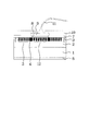
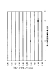
- SiC-JBS structure diode It is sectional drawing for demonstrating a SiC-JBS structure diode. It is a mask layout figure of the SiC Schottky barrier diode shown as a first embodiment. It is sectional drawing for demonstrating the manufacturing process of a SiC-JBS structure diode. It is a figure showing the width of the 1st conductivity type semiconductor of a SiC-JBS structure diode, and the relation of ON resistance. It is a figure showing the width of the 1st conductivity type semiconductor of a SiC-JBS structure diode, and the relation of withstand pressure. It is a mask layout figure of the SiC Schottky barrier diode shown as a second embodiment. It is a mask layout figure of the SiC Schottky barrier diode shown as a third embodiment.
- the present invention relates to a first conductivity type high concentration wide band gap semiconductor substrate, and a first conductivity type low concentration wide band gap semiconductor deposition film formed on the first conductivity type high concentration wide band gap semiconductor substrate And a metal film formed on the low concentration wide band gap semiconductor deposition film of the first conductivity type and forming a Schottky interface region with the low concentration wide band gap semiconductor deposition film of the first conductivity type.
- a second conductivity type region formed in a region corresponding to the metal film peripheral portion of the first conductivity type low concentration wide band gap semiconductor deposited film, the first conductivity type low concentration wide
- the wide band gap semiconductor characterized in that the Schottky interface region in the band gap semiconductor deposited film is surrounded by a region of the second conductivity type to form a plurality of periodic island regions. It is the location.
- the depletion layer spreads by the impurity concentration of the first conductivity type semiconductor and the impurity concentration of the second conductivity type semiconductor. It will be decided.
- the region of the first conductivity type can be depleted from four sides by forming the region of the second conductivity type not in the form of stripes but surrounding the region of the first conductivity type. Therefore, since the voltage for depleting the first conductivity type region of the same area is lowered, the effect of suppressing the leak current and the effect of increasing the impurity concentration of the first conductivity type to reduce the on resistance can be expected. .
- the carrier total amount of the second conductivity type semiconductor region is larger than the carrier total amount of the first conductivity type semiconductor of the area forming the Schottky interface.
- the contact area between the metal film and the island region is S1
- the impurity concentration of the low concentration wide band gap semiconductor deposition film of the first conductivity type is N1
- the metal film and the region of the second conductivity type In the case where the contact area of the semiconductor device is S2 and the impurity concentration of the region of the second conductivity type is N2, it is designed to satisfy S2 ⁇ N2 ⁇ S1 ⁇ N1.
- FIG. 1 is a cross-sectional view of a SiC-JBS diode according to a first embodiment of the present invention.
- a channel stopper 3 having a 6 ⁇ m n-type SiC deposition film 2 and heavily doped with phosphorus, a p-type impurity region 4 heavily doped with aluminum, and aluminum for further dispersing the electric field
- the formed p-type impurity region 5 has six around 1.5 ⁇ m intervals, and on the back surface is formed of silicon oxide with 0.5 ⁇ m thick ohmic electrode 6 Schottky barrier diode 7 having an interlayer insulating film 7, an electrode pad 9 formed of aluminum, and a bonding wire 11 for connection to an external device
- Schottky electrode 8 is made of, for example, titanium silicide and titanium carbide, and p-type impurity region 12 is formed under Schottky electrode 8.
- the Schottky electrode 8 overlaps the p-type impurity region 4 by 4 ⁇ m.
- FIG. 2 is an example of a layout diagram of the SiC Schottky barrier diode shown as the first embodiment of the present invention.
- a cross section taken along the line II of FIG. 2 corresponds to FIG. 1A.
- the channel stopper 3 is disposed to surround the entire structure, and the shape of the Schottky electrode 8 is a square having a curvature of 150 ⁇ m so that concentration of the electric field does not occur at the corners, and the periphery of the Schottky electrode 8 is for termination structure
- the shape of the Schottky electrode 8 is a square having a curvature of 150 ⁇ m so that concentration of the electric field does not occur at the corners, and the periphery of the Schottky electrode 8 is for termination structure
- the electrode pad 9 has a shape, and a passivation film 10 is formed to expose a portion for connection with an external device.
- the bonding wire 11 is connected to the exposed electrode pad 9 for connection to an external device.
- the longest part of the nitrogen-doped n-type layer region is arranged in a square shape of 3 ⁇ m and the island region surrounded by the aluminum-doped p-type region 2 ⁇ m wide is periodic P-type impurity region 12 is formed. From this, it is possible to provide a JBS diode in which the leak current and the on-resistance are suppressed.
- the structure of a Schottky barrier diode manufactured on SiC on a SiC (0001) plane substrate has been described.
- the present invention can be similarly applied to a (000-1) plane substrate, such as a wide GaN
- the metal forming the Schottky interface of the Schottky barrier diode manufactured on the SiC substrate has been described as an example of titanium, the present invention is not limited to titanium, and any material that forms a Schottky interface can be applied similarly.
- the effects of the present invention can be obtained as long as the shape of the island region is a quadrangle, but the shape can be periodically arranged such as a circle, a triangle or a hexagon.
- the impurity region 4 formed in the p-type as the electric field relaxation structure and the impurity region 5 formed in the p-type have exemplified the floating limiting ring (FLR) structure as a structural example, but the junction termination extension (JTE) structure It goes without saying that the effect of the present invention can be obtained with an electric field relaxation structure such as a floating plate structure or the like.
- FLR floating limiting ring
- JTE junction termination extension
- FIGS. 3A to 3F are cross-sectional views showing the manufacturing steps of the JBS structured diode shown in the first embodiment of the present invention.
- 1.8 ⁇ 10 16 cm ⁇ 3 of nitrogen is formed on the surface of high concentration n-type substrate 1 having a (0001) plane with a thickness of 300 ⁇ m doped with 1 ⁇ 10 18 cm ⁇ 3 of nitrogen.
- a 6 ⁇ m thick low concentration n-type deposited film 2 is deposited.
- Phosphorus is implanted into the SiC substrate to form a channel stopper 3 in FIG. 3B.
- aluminum is implanted to form a p-type impurity region 4 for the termination structure, a p-type impurity region 5 for the FLR structure, and a p-type impurity region 12.
- activation is performed at 1650 ° C. for 240 seconds in an Ar atmosphere.
- an ohmic electrode 6 is formed on the back surface of the SiC substrate.
- An interlayer insulating film 7 is formed on the SiC substrate, and titanium is vapor-deposited, for example, in a vacuum at a portion where a Schottky electrode is to be formed, for example, to form a Schottky electrode 8 made of titanium silicide and titanium carbide.
- treatment is performed at 500 ° C. for 5 minutes in an argon atmosphere.
- the end portion of the Schottky electrode 8 is such that the end of the Schottky electrode 8 and the p-type impurity region 4 overlap in order to operate the Schottky barrier diode as a high breakdown voltage element.
- an electrode pad 9 made of aluminum is formed as a pad for connecting the Schottky electrode to an external device.
- a polyimide film is deposited on the surface as a passivation film 10 for preventing discharge due to high voltage, and a bonding wire 11 for connection to an external device is connected to the electrode pad 9.
- FIG. 4 shows the width and 200 A / cm of the n-type layer region doped with nitrogen in the p-type impurity region 12 under the Schottky electrode 8 for the SiC-JBS diode having the periodic structure shown in the first embodiment. It is the relationship of the on resistance when a current of 2 flows. If the width of the n-type impurity region doped with nitrogen in the p-type impurity region 12 below the Schottky electrode 8 is 1 ⁇ m or more, it can be said that the increase in on-resistance can be suppressed.
- FIG. 5 applies the reverse voltage and the width of the n-type layer region of the island region of the p-type impurity region 12 under the Schottky electrode 8 with respect to the SiC-JBS diode having the periodic structure shown in the first embodiment. It is the relationship of the pressure resistance when it did. It can be said that when the width of the island region of the n-type layer region of the p-type impurity region 12 below the Schottky electrode 8 is 4 ⁇ m or less, the reduction in breakdown voltage can be suppressed to 20% or less.
- FIG. 6 is an example of a layout diagram of the SiC Schottky barrier diode shown as the second embodiment.
- the present embodiment is a modification of the shape of the island region with respect to the first embodiment, and is otherwise the same as the first embodiment.
- the longest part of the n-type layer region is arranged in a regular hexagonal shape of 3 .mu.m and surrounded by a 2 .mu.m wide p-type region doped with aluminum.
- the island areas are periodically arranged.
- FIG. 7 is an example of a mask layout diagram of the SiC Schottky barrier diode shown as the third embodiment.
- the present embodiment is a modification of the shape of the island region with respect to the first embodiment, and is otherwise the same as the first and second embodiments.
- an island of an n-type layer region which is disposed in a circular shape having a diameter of 3 ⁇ m in p-type impurity region 12 under Schottky electrode 8 and is surrounded by a 2 ⁇ m wide p-type region doped with aluminum. Regions are periodically arranged.
- the present invention is intended to be an apparatus having a Schottky interface formed on a wide band gap semiconductor. It is needless to say that the present invention can be applied to a structure which does not deviate from the above, for example, a DMT structure using a Schottky barrier, and an apparatus using a Schottky junction such as a diode having a TMBS structure.
Landscapes
- Electrodes Of Semiconductors (AREA)
Abstract
La présente invention concernant un dispositif de semi-conducteur à large bande interdite aborde le problème de supprimer une augmentation d'un courant de fuite et une augmentation de résistance à l'état passant lorsqu'une tension inverse est appliquée au dispositif ayant une interface entre un métal et un semi-conducteur à large bande interdite. Ledit dispositif de semi-conducteur à large bande interdite comprend : un substrat de semi-conducteur à large bande interdite de premier type de conductivité ayant une concentration élevée ; un film de dépôt de semi-conducteur à large bande interdite de premier type de conductivité ayant une faible concentration, ledit film de dépôt de semi-conducteur étant formé sur le substrat semi-conducteur ; un film métallique, qui est formé sur le film de dépôt de semi-conducteur, et qui constitue une région d'interface Schottky entre le film métallique et le film de dépôt de semi-conducteur ; et une région de second type de conductivité, qui est formée dans une région qui correspond à la périphérie du film métallique sur le film de dépôt de semi-conducteur. La région d'interface Schottky sur le film de dépôt de semi-conducteur est entourée par la région du second type de conductivité et constitue une pluralité de régions d'îlots à des intervalles réguliers.
Priority Applications (2)
| Application Number | Priority Date | Filing Date | Title |
|---|---|---|---|
| PCT/JP2012/053506 WO2013121532A1 (fr) | 2012-02-15 | 2012-02-15 | Dispositif semi-conducteur à large bande interdite |
| US14/365,152 US9455326B2 (en) | 2012-02-15 | 2012-02-15 | Wide bandgap semiconductor device |
Applications Claiming Priority (1)
| Application Number | Priority Date | Filing Date | Title |
|---|---|---|---|
| PCT/JP2012/053506 WO2013121532A1 (fr) | 2012-02-15 | 2012-02-15 | Dispositif semi-conducteur à large bande interdite |
Publications (1)
| Publication Number | Publication Date |
|---|---|
| WO2013121532A1 true WO2013121532A1 (fr) | 2013-08-22 |
Family
ID=48983694
Family Applications (1)
| Application Number | Title | Priority Date | Filing Date |
|---|---|---|---|
| PCT/JP2012/053506 Ceased WO2013121532A1 (fr) | 2012-02-15 | 2012-02-15 | Dispositif semi-conducteur à large bande interdite |
Country Status (2)
| Country | Link |
|---|---|
| US (1) | US9455326B2 (fr) |
| WO (1) | WO2013121532A1 (fr) |
Cited By (3)
| Publication number | Priority date | Publication date | Assignee | Title |
|---|---|---|---|---|
| CN104465794A (zh) * | 2013-09-24 | 2015-03-25 | 三垦电气株式会社 | 半导体装置 |
| JP2016004965A (ja) * | 2014-06-19 | 2016-01-12 | 株式会社東芝 | 半導体装置 |
| JP2018107399A (ja) * | 2016-12-28 | 2018-07-05 | 新電元工業株式会社 | 半導体装置 |
Families Citing this family (11)
| Publication number | Priority date | Publication date | Assignee | Title |
|---|---|---|---|---|
| CA2872941C (fr) * | 2012-05-17 | 2021-03-30 | General Electric Company | Dispositif a semi-conducteur a extension de terminaison de jonction |
| US9006748B2 (en) * | 2012-12-03 | 2015-04-14 | Panasonic Intellectual Property Management Co., Ltd. | Semiconductor device and method for manufacturing same |
| JP2015032627A (ja) * | 2013-07-31 | 2015-02-16 | 株式会社東芝 | 半導体装置 |
| JP6745458B2 (ja) * | 2015-04-15 | 2020-08-26 | パナソニックIpマネジメント株式会社 | 半導体素子 |
| JP6371924B1 (ja) | 2015-07-03 | 2018-08-08 | アーベーベー・シュバイツ・アーゲー | 向上したサージ電流能力を有する接合障壁ショットキーダイオード |
| JP6719090B2 (ja) * | 2016-12-19 | 2020-07-08 | パナソニックIpマネジメント株式会社 | 半導体素子 |
| WO2019013136A1 (fr) * | 2017-07-08 | 2019-01-17 | 株式会社Flosfia | Dispositif à semi-conducteur |
| EP3712962B1 (fr) * | 2019-03-22 | 2023-06-07 | STMicroelectronics S.r.l. | Diode mps semiconductrice avec réduction de l'effet de tassement de courant et son procédé de fabrication |
| CN113990956B (zh) | 2020-07-27 | 2026-02-27 | 意法半导体股份有限公司 | 基于SiC的可扩展MPS器件 |
| IT202000018127A1 (it) * | 2020-07-27 | 2022-01-27 | St Microelectronics Srl | Dispositivo mps scalabile basato su sic, metodo di fabbricazione del dispositivo mps e apparecchio elettronico comprendente il dispositivo mps |
| JP7697255B2 (ja) * | 2021-04-27 | 2025-06-24 | 富士電機株式会社 | 炭化珪素半導体装置および炭化珪素半導体装置の製造方法 |
Citations (3)
| Publication number | Priority date | Publication date | Assignee | Title |
|---|---|---|---|---|
| JP2002314098A (ja) * | 2001-04-13 | 2002-10-25 | Sanken Electric Co Ltd | 半導体装置 |
| JP2009094433A (ja) * | 2007-10-12 | 2009-04-30 | National Institute Of Advanced Industrial & Technology | 炭化珪素装置 |
| JP2010087483A (ja) * | 2008-09-08 | 2010-04-15 | Mitsubishi Electric Corp | 半導体装置 |
Family Cites Families (8)
| Publication number | Priority date | Publication date | Assignee | Title |
|---|---|---|---|---|
| JP3943749B2 (ja) | 1999-02-26 | 2007-07-11 | 株式会社日立製作所 | ショットキーバリアダイオード |
| JP2006352006A (ja) | 2005-06-20 | 2006-12-28 | Sumitomo Electric Ind Ltd | 整流素子およびその製造方法 |
| US20070228505A1 (en) * | 2006-04-04 | 2007-10-04 | Mazzola Michael S | Junction barrier schottky rectifiers having epitaxially grown p+-n junctions and methods of making |
| JP4375439B2 (ja) | 2007-05-30 | 2009-12-02 | 株式会社デンソー | ジャンクションバリアショットキーダイオードを備えた炭化珪素半導体装置 |
| JP4333782B2 (ja) | 2007-07-05 | 2009-09-16 | 株式会社デンソー | ジャンクションバリアショットキーダイオードを備えた炭化珪素半導体装置 |
| JP5083885B2 (ja) | 2007-11-20 | 2012-11-28 | 日本インター株式会社 | Jbsおよびmosfet |
| JP2009158519A (ja) | 2007-12-25 | 2009-07-16 | Toyota Motor Corp | 半導体装置及びその製造方法 |
| JP2010040857A (ja) | 2008-08-06 | 2010-02-18 | Toshiba Corp | 半導体装置 |
-
2012
- 2012-02-15 WO PCT/JP2012/053506 patent/WO2013121532A1/fr not_active Ceased
- 2012-02-15 US US14/365,152 patent/US9455326B2/en not_active Expired - Fee Related
Patent Citations (3)
| Publication number | Priority date | Publication date | Assignee | Title |
|---|---|---|---|---|
| JP2002314098A (ja) * | 2001-04-13 | 2002-10-25 | Sanken Electric Co Ltd | 半導体装置 |
| JP2009094433A (ja) * | 2007-10-12 | 2009-04-30 | National Institute Of Advanced Industrial & Technology | 炭化珪素装置 |
| JP2010087483A (ja) * | 2008-09-08 | 2010-04-15 | Mitsubishi Electric Corp | 半導体装置 |
Cited By (4)
| Publication number | Priority date | Publication date | Assignee | Title |
|---|---|---|---|---|
| CN104465794A (zh) * | 2013-09-24 | 2015-03-25 | 三垦电气株式会社 | 半导体装置 |
| JP2016004965A (ja) * | 2014-06-19 | 2016-01-12 | 株式会社東芝 | 半導体装置 |
| CN105280724A (zh) * | 2014-06-19 | 2016-01-27 | 株式会社东芝 | 半导体装置 |
| JP2018107399A (ja) * | 2016-12-28 | 2018-07-05 | 新電元工業株式会社 | 半導体装置 |
Also Published As
| Publication number | Publication date |
|---|---|
| US20140327019A1 (en) | 2014-11-06 |
| US9455326B2 (en) | 2016-09-27 |
Similar Documents
| Publication | Publication Date | Title |
|---|---|---|
| WO2013121532A1 (fr) | Dispositif semi-conducteur à large bande interdite | |
| JP2012094683A (ja) | ワイドバンドギャップ半導体装置 | |
| JP6053103B2 (ja) | ワイドバンドギャップ半導体装置およびその製造方法 | |
| JP2015207780A (ja) | ワイドバンドギャップ半導体装置 | |
| US10090417B2 (en) | Silicon carbide semiconductor device and fabrication method of silicon carbide semiconductor device | |
| US20080083966A1 (en) | Schottky barrier semiconductor device | |
| JP5943819B2 (ja) | 半導体素子、半導体装置 | |
| US9142687B2 (en) | Semiconductor diode device | |
| US9178079B2 (en) | Semiconductor diode device | |
| JP5106604B2 (ja) | 半導体装置およびその製造方法 | |
| JP2016208030A (ja) | 半導体素子及びその製造方法 | |
| US11869944B2 (en) | Scalable MPS device based on SiC | |
| US12224321B2 (en) | Scalable MPS device based on SiC | |
| WO2015008385A1 (fr) | Module de puissance | |
| JP6384944B2 (ja) | 炭化珪素半導体装置および炭化珪素半導体装置の製造方法 | |
| CN108538925A (zh) | 一种碳化硅结势垒肖特基二极管 | |
| CN106298775B (zh) | 一种混合整流二极管及其制作方法 | |
| CN112909098A (zh) | 一种肖特基二极管及其制备方法 | |
| JP2012227419A (ja) | ワイドギャップ半導体装置 | |
| JP2015029099A (ja) | 窒化ガリウム系ダイオード及びその製造方法 | |
| JP2015149375A (ja) | ダイオード | |
| JP6609283B2 (ja) | 炭化珪素半導体装置 | |
| CN222954304U (zh) | 一种碳化硅肖特基二极管器件 | |
| JP2012094889A (ja) | 半導体装置 | |
| CN103094357A (zh) | 半导体器件 |
Legal Events
| Date | Code | Title | Description |
|---|---|---|---|
| 121 | Ep: the epo has been informed by wipo that ep was designated in this application |
Ref document number: 12868669 Country of ref document: EP Kind code of ref document: A1 |
|
| WWE | Wipo information: entry into national phase |
Ref document number: 14365152 Country of ref document: US |
|
| NENP | Non-entry into the national phase |
Ref country code: DE |
|
| 122 | Ep: pct application non-entry in european phase |
Ref document number: 12868669 Country of ref document: EP Kind code of ref document: A1 |
|
| NENP | Non-entry into the national phase |
Ref country code: JP |